EP3817018A1 - Electronic device - Google Patents
Electronic device Download PDFInfo
- Publication number
- EP3817018A1 EP3817018A1 EP18924813.1A EP18924813A EP3817018A1 EP 3817018 A1 EP3817018 A1 EP 3817018A1 EP 18924813 A EP18924813 A EP 18924813A EP 3817018 A1 EP3817018 A1 EP 3817018A1
- Authority
- EP
- European Patent Office
- Prior art keywords
- primary
- coil
- electronic element
- sealing part
- electronic
- Prior art date
- Legal status (The legal status is an assumption and is not a legal conclusion. Google has not performed a legal analysis and makes no representation as to the accuracy of the status listed.)
- Pending
Links
Images







Classifications
-
- H—ELECTRICITY
- H01—ELECTRIC ELEMENTS
- H01F—MAGNETS; INDUCTANCES; TRANSFORMERS; SELECTION OF MATERIALS FOR THEIR MAGNETIC PROPERTIES
- H01F27/00—Details of transformers or inductances, in general
- H01F27/28—Coils; Windings; Conductive connections
- H01F27/2804—Printed windings
-
- H—ELECTRICITY
- H01—ELECTRIC ELEMENTS
- H01F—MAGNETS; INDUCTANCES; TRANSFORMERS; SELECTION OF MATERIALS FOR THEIR MAGNETIC PROPERTIES
- H01F27/00—Details of transformers or inductances, in general
- H01F27/28—Coils; Windings; Conductive connections
- H01F27/30—Fastening or clamping coils, windings, or parts thereof together; Fastening or mounting coils or windings on core, casing, or other support
- H01F27/306—Fastening or mounting coils or windings on core, casing or other support
-
- H—ELECTRICITY
- H01—ELECTRIC ELEMENTS
- H01F—MAGNETS; INDUCTANCES; TRANSFORMERS; SELECTION OF MATERIALS FOR THEIR MAGNETIC PROPERTIES
- H01F30/00—Fixed transformers not covered by group H01F19/00
- H01F30/06—Fixed transformers not covered by group H01F19/00 characterised by the structure
-
- H—ELECTRICITY
- H01—ELECTRIC ELEMENTS
- H01F—MAGNETS; INDUCTANCES; TRANSFORMERS; SELECTION OF MATERIALS FOR THEIR MAGNETIC PROPERTIES
- H01F30/00—Fixed transformers not covered by group H01F19/00
- H01F30/06—Fixed transformers not covered by group H01F19/00 characterised by the structure
- H01F30/10—Single-phase transformers
-
- H—ELECTRICITY
- H01—ELECTRIC ELEMENTS
- H01F—MAGNETS; INDUCTANCES; TRANSFORMERS; SELECTION OF MATERIALS FOR THEIR MAGNETIC PROPERTIES
- H01F27/00—Details of transformers or inductances, in general
- H01F27/28—Coils; Windings; Conductive connections
- H01F27/2804—Printed windings
- H01F2027/2819—Planar transformers with printed windings, e.g. surrounded by two cores and to be mounted on printed circuit
-
- H—ELECTRICITY
- H01—ELECTRIC ELEMENTS
- H01F—MAGNETS; INDUCTANCES; TRANSFORMERS; SELECTION OF MATERIALS FOR THEIR MAGNETIC PROPERTIES
- H01F27/00—Details of transformers or inductances, in general
- H01F27/28—Coils; Windings; Conductive connections
- H01F27/32—Insulating of coils, windings, or parts thereof
- H01F27/327—Encapsulating or impregnating
Definitions
- the present invention relates to an electronic device that has a primary coil and a secondary coil.
- JP 2008-502166 A discloses that a primary coil, a secondary coil, and a core are included, and coil layers of the secondary coil are wound to be superimposed onto each other, in principle, in a direction that is parallel to a plane of the primary coil. More specifically, the primary coil is constituted of one layer, the secondary coil is constituted of multiple layers, and an insulating material is provided between both.
- manufacture can be easily performed, but there has been room for improvement in transmission efficiency in a transformer.
- the present invention provides an electronic device that can be reduced in size, and can also enhance transmission efficiency in a transformer.
- the primary coil has the primary-side first coil that is provided on the other side of the secondary coil, and the primary-side second coil that is provided on the one side of the secondary coil, and the connecting part connecting the primary-side first coil and the primary-side second coil is provided and passes through the secondary coil has been employed, a size of an electronic device can be reduced. Furthermore, the primary-side first coil and the primary-side second coil can be provided to sandwich the secondary coil, and therefore transmission efficiency in a transformer can also be enhanced.
- one side means an upper side in Fig. 3
- another side means a lower side in Fig. 3
- An upward or downward direction in Fig. 3 is referred to as a "first direction”
- a leftward or rightward direction is referred to as a “second direction”
- directions of front and reverse sides of paper are referred to as a "third direction”.
- An in-plane direction including the second direction and the third direction is referred to as a "plane direction”.
- an electronic device may have a primary coil 10, a secondary coil 20 that is disposed to face the primary coil 10, a primary-side electronic element 110 that is electrically connected to the primary coil 10, and a secondary-side electronic element 210 that is electrically connected to the secondary coil 20.
- the primary coil 10 may have a primary-side first coil 10a that is provided on another side of the secondary coil 20, and a primary-side second coil 10b that is provided on one side of the primary-side first coil 10a.
- a connecting part 19 connecting the primary-side first coil 10a and the primary-side second coil 10b may be provided and may pass through a space in a plane direction of the primary-side second coil 10b.
- the primary coil 10 may be constituted of a lead frame.
- a thickness of the secondary coil 20 may be greater than a thickness of the primary coil 10.
- the secondary coil 20 may be provided with a gap G without being wound one turn or more.
- the secondary coil 20 may have a secondary coil part 21 and a pair of secondary-side extension parts 70 that extend from both ends of the secondary coil part 21 to be integrated with the secondary coil part 21, and may be provided with the gap G between the pair of secondary-side extension parts 70.
- the connecting part 19 may pass through the secondary coil 20 between both ends of the secondary coil part 21 or between the pair of the secondary-side extension parts 70.
- the connecting part 19 does not need to be completely parallel to the first direction, and may be inclined with respect to the first direction.
- An aspect of "extending along the first direction” also includes an aspect of extending to be inclined with respect to the first direction, as described above.
- the secondary coil 20 may be provided on the one side of the primary-side second coil 10b, or the secondary coil 20 may be provided on the other side of the primary-side first coil 10a.
- a coil sealing part 50 sealing the primary coil 10, the secondary coil 20, and the connecting part 19 and being made of sealing resin or the like may be provided.
- a first electronic module 100 that has the primary-side electronic element 110 and the primary-side sealing part 150 may be provided. As illustrated in Fig. 1 , the first electronic module 100 may have a primary-side substrate 120, a plurality of primary-side conductor layers 130 that is provided on one surface of the primary-side substrate 120, and a primary-side electronic element 110 that is provided on one surface of the primary-side conductor layer 130.
- the primary-side electronic element 110, a surface on the one side of the primary-side substrate 120, and a surface on the one side of the primary-side conductor layer 130 may be sealed with the primary-side sealing part 150 (see Fig. 5 ).
- the primary-side sealing part 150 may be constituted of primary-side sealing resin.
- a primary-side first electrode (for example, a source electrode) 111 and a primary-side second electrode (for example, a gate electrode) 112 may be provided on one surface of the primary-side electronic element 110, and a primary-side third electrode (for example, a drain electrode) 113 may be provided on another surface of the primary-side electronic element 110.
- the primary-side first electrode 111 and the primary-side conductor layer 130 may be connected via a primary-side first connector 116 (see Fig. 1 ) and a conductive adhesive (not illustrated) such as solder.
- the primary-side second electrode 112 and the primary-side conductor layer 130 may be connected via a primary-side second connector 117 (see Fig.
- the primary-side first electrode 111 may be provided on one surface of the primary-side electronic element 110, and the primary-side second electrode 112 may be provided on another surface of the primary-side electronic element 110.
- a second electronic module 200 that has the secondary-side electronic element 210 and the secondary-side sealing part 250 (see Fig. 5 ) may be provided.
- the second electronic module 200 may have a secondary-side substrate 220, a plurality of secondary-side conductor layers 230 that is provided on one surface of the secondary-side substrate 220, and a secondary-side electronic element 210 that is provided on one surface of the secondary-side conductor layer 230.
- the secondary-side electronic element 210, a surface on the one side of the secondary-side substrate 220, and a surface on the one side of the secondary-side conductor layer 230 may be sealed with the secondary-side sealing part 250 (see Fig. 5 ).
- the secondary-side sealing part 250 may be constituted of secondary-side sealing resin.
- the primary-side sealing resin and the secondary-side sealing resin may be constituted of the same resin material, or may be constituted of resin materials that are different from each other.
- a secondary-side first electrode 211 may be provided on one surface of the secondary-side electronic element 210, and a secondary-side second electrode 212 may be provided on another surface of the secondary-side electronic element 210.
- the secondary-side first electrode 211 and the secondary-side conductor layer 230 may be connected via a secondary-side first connector 216 (see Fig. 1 ) and a conductive adhesive such as solder.
- a secondary-side first connector 216 see Fig. 1
- a conductive adhesive such as solder.
- the secondary-side first electrode (for example, a source electrode) 211 and the secondary-side second electrode (for example, a gate electrode) 212 may be provided on one surface of the secondary-side electronic element 210, and a secondary-side third electrode (for example, a drain electrode) 213 may be provided on another surface of the secondary-side electronic element 210.
- the secondary-side third electrode 213 and the secondary-side conductor layer 230 may be connected via a conductive adhesive such as solder.
- the primary-side first coil 10a and the primary-side second coil 10b of the primary coil 10 may have the same number of turns, or may have numbers of turns that are different from each other.
- each of the numbers of turns of the primary-side first coil 10a and the primary-side second coil 10b of the primary coil 10 may be 4.5.
- the number of turns of the secondary coil 20 may be 1, or may be 2 or more.
- the primary coil 10 and a primary-side extension part 60 that extends to an inside of the primary-side sealing part 150 may be integrated.
- the primary-side extension part 60 may have a primary-side first extension part 60a, and a primary-side second extension part 60b that is located on the one side relative to the primary-side first extension part 60a.
- the primary-side first coil 10a and the primary-side first extension part 60a may be integrated, and the primary-side second coil 10b and the primary-side second extension part 60b may be integrated.
- a core 500 such as an E-core that passes through the primary coil 10 and the secondary coil 20 may be provided.
- the core 500 may have a leg part 510, and the leg part 510 may be provided to pass through an opening part 51 that is provided in the coil sealing part 50.
- the leg part 510 of the core 500 may be provided to abut onto an inner peripheral surface of the coil sealing part 50.
- An outer peripheral part of the core 500 may be provided to cover an outer periphery of the coil sealing part 50.
- the primary coil 10 has the primary-side first coil 10a that is provided on the other side of the secondary coil 20, and the primary-side second coil 10b that is provided on the one side of the secondary coil 20, and the connecting part 19 connecting the primary-side first coil 10a and the primary-side second coil 10b is provided and passes through the secondary coil 20 has been employed, a wiring length between the primary-side electronic element 110 and the primary coil 10 can be reduced, a wiring length between the secondary-side electronic element 210 and the secondary coil 20 can be reduced, and a size of an electronic device can be reduced. Furthermore, the primary-side first coil 10a and the primary-side second coil 10b can be provided to sandwich the secondary coil 20, and therefore transmission efficiency in a transformer can also be enhanced.
- a member in which the secondary coil 20 and the secondary-side extension parts 70 that extend to the inside of the secondary-side sealing part 250 are integrated can be easily manufactured, by forming the secondary coil 20 and the secondary-side extension parts 70 in a member such as a lead frame and removing an unnecessary portion.
- a cooling body such as a heat sink may be provided on another surface (a back surface) of the coil sealing part 50, another surface (a back surface) of the primary-side sealing part 150, and another surface (a back surface) of the secondary-side sealing part 250.
- a cooling body such as a heat sink may be provided on another surface (a back surface) of the coil sealing part 50, another surface (a back surface) of the primary-side sealing part 150, and another surface (a back surface) of the secondary-side sealing part 250.
- the primary-side electronic element 110 has a primary-side first electronic element 110a, and a primary-side second electronic element 110b that is provided on the one side relative to the primary-side first electronic element 110a.
- the primary-side first electronic element 110a may be provided on the primary-side first extension part 60a that extends from the primary-side first coil 10a, and may be electrically connected to the primary-side first coil 10a.
- the primary-side second electronic element 110b may be provided on the primary-side second extension part 60b that extends from the primary-side second coil 10b, and may be electrically connected to the primary-side second coil 10b.
- the other configuration is similar to a configuration in the first embodiment, and all of the aspects described in the first embodiment can be employed.
- the members described in the first embodiment are described by using the same reference signs.
- the primary-side electronic element 110 may be sealed with the primary-side sealing part 150.
- the secondary-side electronic element 210 may be sealed with the secondary-side sealing part 250.
- the primary-side first electronic element 110a is provided on the primary-side first extension part 60a that extends from the primary-side first coil 10a to an outside of the coil sealing part 50 may be employed. In this case, wiring length can be further reduced, and the size of the electronic device can be reduced.
- the primary-side second electronic element 110b is provided on the primary-side second extension part 60b that extends from the primary-side second coil 10b to the outside of the coil sealing part 50 may be employed. In this case, similarly, wiring length can be further reduced, and the size of the electronic device can be reduced.
- the primary-side first electronic element 110a may be provided on the primary-side first extension part 60a via a conductive adhesive such as solder, and the primary-side second electronic element 110b may be provided on the primary-side second extension part 60b via a conductive adhesive such as solder.
- the primary-side first extension part 60a and the primary-side second extension part 60b are provided on the other side and the one side of the secondary-side coil 20, and the primary-side first extension part 60a and the primary-side second extension part 60b are disposed to be spaced apart from each other in the first direction.
- This can suppress an influence of noise or the like that occurs from the primary-side first electronic element 110a that is provided on one surface of the primary-side first extension part 60a on the primary-side second electronic element 110b that is provided on one surface of the primary-side second extension part 60b, or in contrast, an influence of noise or the like that occurs from the primary-side second electronic element 110b on the primary-side first electronic element 110a.
- the primary-side electronic element 110 may be provided on each of the one side and the other side of the primary-side extension part 60.
- a primary-side connecting body 190 that connects a plurality of primary-side electronic elements 110 that is provided on the one side of the primary-side extension part 60 may be provided.
- a primary-side first electrode (for example, a source electrode) 111 (see Fig. 7 ) of a primary-side electronic element 110 that is located on the other side of the primary-side extension part 60 and a primary-side third electrode (for example, a drain electrode) 113 (see Fig.
- primary-side first electrodes (for example, source electrodes) 111 of a plurality of primary-side electronic elements 110 that is located on the one side of the primary-side extension part 60 may be electrically connected by the primary-side connecting body 190 (see a primary-side electronic element 110 that is located on a leftmost side and a primary-side electronic element 110 that is located on a rightmost side in Fig. 12 ).
- the secondary-side electronic element 210 is provided on the secondary-side extension part 70 that extends from the secondary coil 20 to the outside of the coil sealing part 50 .
- the other configuration is similar to a configuration in the first embodiment or the second embodiment, and all of the aspects described in each of the embodiments described above can be employed.
- the members described in each of the embodiments described above are described by using the same reference signs.
- the secondary-side electronic element 210 is provided on the secondary-side extension part 70 that extends from the secondary coil 20 to the outside of the coil sealing part 50, as in the present embodiment, has been employed, wiring length can be further reduced, and the size of the electronic device can be reduced.
- the secondary-side electronic element 210 may be provided on the secondary-side extension part 70 via a conductive adhesive such as solder. As illustrated in Fig. 13 , a widthwise length of a base end 71 of the secondary-side extension part 70 may be longer in the third direction than a widthwise length of the secondary-side electronic element 210, and the secondary-side electronic element 210 may be placed on the base end 71.
- the secondary-side electronic element 210 may be provided on each of the one side and the other side of the secondary-side extension part 70.
- a secondary-side connecting body 290 that connects a plurality of secondary-side electronic elements 210 that is provided on the one side of the secondary-side extension part 70 may be provided.
- a secondary-side first electrode (for example, a source electrode) 211 (see Fig. 7 ) of a secondary-side electronic element 210 that is located on the other side of the secondary-side extension part 70 and a secondary-side third electrode (for example, a drain electrode) 213 (see Fig.
- secondary-side first electrodes (for example, source electrodes) 211 of a plurality of secondary-side electronic elements 210 that is located on the one side of the secondary-side extension part 70 may be electrically connected by the secondary-side connecting body 290 (see two secondary-side electronic elements 210 that are disposed on left-hand and right-hand sides on an upper side in Fig. 14 ).
- a first bent part 310 is provided in the primary-side extension part 60 between the coil sealing part 50 and the primary-side sealing part 150 .
- the other configuration is similar to configurations in the first to third embodiments, and all of the aspects described in each of the embodiments described above can be employed.
- the members described in each of the embodiments described above are described by using the same reference signs.
- the coil sealing part 50 and the secondary-side sealing part 250 can be disposed along a plane direction, and the primary-side sealing part 150 can be disposed along a direction that is bent by a predetermined angle (for example, 60 degrees, 90 degrees, 120 degrees, or the like) with respect to the plane direction. Therefore, a size in a certain plane direction can be reduced.
- a predetermined angle for example, 60 degrees, 90 degrees, 120 degrees, or the like
- such bending enables a reduction in an influence of noise or the like generated in the primary-side electronic element 110 sealed with the primary-side sealing part 150 on the secondary-side electronic element 210 sealed with the secondary-side sealing part 250, and also enables a reduction in an influence of noise or the like generated in the secondary-side electronic element 210 on the secondary-side electronic element 210 sealed with the primary-side sealing part 150.
- the cooling body 350 such as a heat sink may be provided on the back surface of the coil sealing part 50, the back surface of the primary-side sealing part 150, and the back surface of the secondary-side sealing part 250.
- the cooling body 350 such as a heat sink may be provided on the back surface of the coil sealing part 50, the back surface of the primary-side sealing part 150, and the back surface of the secondary-side sealing part 250.
- a second bent part 320 is provided in the secondary-side extension part 70 between the coil sealing part 50 and the secondary-side sealing part 250 .
- the other configuration is similar to configurations in the first to third embodiments, and all of the aspects described in each of the embodiments described above can be employed.
- the members described in each of the embodiments described above are described by using the same reference signs.
- the coil sealing part 50 and the primary-side sealing part 150 can be disposed along a plane direction, and the secondary-side sealing part 250 can be disposed along a direction that is bent by a predetermined angle (for example, 60 degrees, 90 degrees, 120 degrees, or the like) with respect to the plane direction. Therefore, a size in a certain plane direction can be reduced.
- a predetermined angle for example, 60 degrees, 90 degrees, 120 degrees, or the like
- such bending enables a reduction in an influence of noise or the like generated in the primary-side electronic element 110 sealed with the primary-side sealing part 150 on the secondary-side electronic element 210 sealed with the secondary-side sealing part 250, and also enables a reduction in an influence of noise or the like generated in the secondary-side electronic element 210 on the secondary-side electronic element 210 sealed with the primary-side sealing part 150.
- the cooling body 350 such as a heat sink may be provided on the back surface of the coil sealing part 50, the back surface of the primary-side sealing part 150, and the back surface of the secondary-side sealing part 250.
- the cooling body 350 such as a heat sink may be provided on the back surface of the coil sealing part 50, the back surface of the primary-side sealing part 150, and the back surface of the secondary-side sealing part 250.
- the first bent part 310 is provided in the primary-side extension part 60 between the coil sealing part 50 and the primary-side sealing part 150 and the second bent part 320 is provided in the s secondary-side extension part 70 between the coil sealing part 50 and the secondary-side sealing part 250 is employed.
- the other configuration is similar to a configuration in the first to third embodiments, and all of the aspects described in each of the embodiments described above can be employed.
- the members described in each of the embodiments described above are described by using the same reference signs.
- the coil sealing part 50, the primary-side sealing part 150, and the secondary-side sealing part 250 can be respectively disposed along plane directions that are different from each other. Furthermore, the primary-side sealing part 150 and the secondary-side sealing part 250 can also be disposed in such a way that respective back surfaces face each other.
- the coil sealing part 50 and the primary-side sealing part 150 may be disposed to be bent by a first angle (for example, 60 degrees, 90 degrees, 120 degrees, or the like) with respect to each other, and the coil sealing part 50 and the secondary-side sealing part 250 may be disposed to be bent by a second angle (for example, 60 degrees, 90 degrees, 120 degrees, or the like) with respect to each other.
- the cooling body 350 such as a heat sink may be provided on the back surface of the coil sealing part 50, the back surface of the primary-side sealing part 150, and the back surface of the secondary-side sealing part 250.
- the cooling body 350 such as a heat sink may be provided on the back surface of the coil sealing part 50, the back surface of the primary-side sealing part 150, and the back surface of the secondary-side sealing part 250.
- disposition can be performed in such a way that the back surface of the coil sealing part 50, the back surface of the primary-side sealing part 150, and the back surface of the secondary-side sealing part 250 respectively abut onto three surfaces of the cooling body 350 that is made of a heat sink or the like, and there is an advantage in which a high cooling effect can be expected.
- the primary-side terminal 60 and the secondary-side terminal 70 do not need to be provided linearly.
- the primary-side terminal 60 and the secondary-side terminal 70 may be provided to be orthogonal to each other in a plane direction, or may be provided to cross each other at an angle that is different from 90 degrees in the plane direction.
- Fig. 18 illustrates an aspect in which the primary-side terminal 60 and the secondary-side terminal 70 are orthogonal to each other in the plane direction.
- the primary-side sealing part 150 and the secondary-side sealing part 250 can be disposed in any direction of the plane direction, and can be bent by using the first bent part 310 and the second bent part 320.
Landscapes
- Engineering & Computer Science (AREA)
- Power Engineering (AREA)
- Coils Or Transformers For Communication (AREA)
- Coils Of Transformers For General Uses (AREA)
- Dc-Dc Converters (AREA)
Abstract
Description
- The present invention relates to an electronic device that has a primary coil and a secondary coil.
- Conventionally, a transformer that has a primary coil and a secondary coil is known. For example,
JP 2008-502166 A - As described above, in an aspect in which a primary coil and a secondary coil are superimposed onto each other via an insulating material, manufacture can be easily performed, but there has been room for improvement in transmission efficiency in a transformer.
- The present invention provides an electronic device that can be reduced in size, and can also enhance transmission efficiency in a transformer.
-
- [Concept 1]
An electronic device may comprise:- a primary coil;
- a secondary coil disposed to face the primary coil;
- a primary-side electronic element electrically connected to the primary coil; and
- a secondary-side electronic element electrically connected to the secondary coil, wherein
- the primary coil may have a primary-side first coil that is provided on another side of the secondary coil, and a primary-side second coil that is provided on one side of the primary-side first coil, and
- a connecting part connecting the primary-side first coil and the primary-side second coil may be provided and may pass through a space of the secondary coil.
- [Concept 2]
In the electronic device according to concept 1,
the secondary coil may have a secondary coil part and a pair of secondary-side extension parts that extend from both ends of the secondary coil part, and
the connecting part may pass through the space of the secondary coil between the both ends of the secondary coil part or between the pair of the secondary-side extension parts. - [Concept 3]
The electronic device according to concept 1 or 2 may further comprise a coil sealing part sealing the primary coil, the secondary coil, and the connecting part. - [Concept 4]
In the electronic device according to any one of concepts 1 to 3,
the primary-side electronic element may have a primary-side first electronic element and a primary-side second electronic element provided on one side relative to the primary-side first electronic element,
the primary-side first electronic element may be electrically connected to the primary-side first coil, and
the primary-side second electronic element may be electrically connected to the primary-side second coil. - [Concept 5]
In the electronic device according to concept 4,
the primary-side first electronic element may be provided on a primary-side first extension part that extends from the primary-side first coil, or the primary-side second electronic element may be provided on a primary-side second extension part that extends from the primary-side second coil. - [Concept 6]
The electronic device according to any one of concepts 1 to 5 may further comprise a primary-side sealing part sealing the primary-side electronic element, or a secondary-side sealing part sealing the secondary-side electronic element. - [Concept 7]
The electronic device according to any one of concepts 1 to 6 may further comprise a first electronic module having the primary-side electronic element, a primary-side substrate on which the primary-side electronic element is provided and a primary-side sealing part sealing the primary-side electronic element, or a second electronic module having the secondary-side electronic element, a secondary-side substrate on which the secondary-side electronic element is provided and a secondary-side sealing part sealing the secondary-side electronic element. - [Concept 8]
In the electronic device according to any one of concepts 1 to 7,
the primary-side first coil or the primary-side second coil may be made from a lead frame. - As an aspect of the present invention, in a case where an aspect where the primary-side electronic element that is electrically connected to the primary coil and the secondary-side electronic element that is electrically connected to the secondary coil are provided, the primary coil has the primary-side first coil that is provided on the other side of the secondary coil, and the primary-side second coil that is provided on the one side of the secondary coil, and the connecting part connecting the primary-side first coil and the primary-side second coil is provided and passes through the secondary coil has been employed, a size of an electronic device can be reduced. Furthermore, the primary-side first coil and the primary-side second coil can be provided to sandwich the secondary coil, and therefore transmission efficiency in a transformer can also be enhanced.
-
-
Fig. 1 is a plan view illustrating a state before an electronic device that can be used in a first embodiment of the present invention is separated from a lead frame. -
Fig. 2 is a plan view illustrating a primary coil that can be used in the first embodiment of the present invention. -
Fig. 3 is a side view in which the primary coil and a secondary coil that can be used in the first embodiment of the present invention are viewed along a third direction. -
Fig. 4 is a side view in which the primary coil and the secondary coil that can be used in the first embodiment of the present invention are viewed along a second direction. -
Fig. 5 is a plan view that illustrates a coil sealing part, a primary-side sealing part, and a secondary-side sealing part that can be used in the first embodiment of the present invention, and corresponds toFig. 1 . -
Fig. 6 is a perspective view illustrating the secondary coil that can be used in the first embodiment of the present invention. -
Fig. 7 is a side sectional view illustrating a primary-side electronic element and a secondary-side electronic element that can be used in the first embodiment of the present invention. -
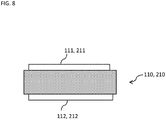
Fig. 8 is a side sectional view illustrating another aspect of the primary-side electronic element and the secondary-side electronic element that can be used in the first embodiment of the present invention. -
Fig. 9 is a side view illustrating a relationship between the coil sealing part and a core that can be used in the first embodiment of the present invention. -
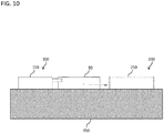
Fig. 10 is a side view illustrating a relationship between the coil sealing part, the primary-side sealing part, and the secondary-side sealing part, and a cooling body that can be used in the first embodiment of the present invention. -
Fig. 11 is a side view illustrating an aspect on a side of a first electronic module that can be used in a second embodiment of the present invention. -
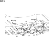
Fig. 12 is a perspective view illustrating an aspect that can be used in the second embodiment of the present invention, and is different from the aspect illustrated inFig. 11 . -
Fig. 13 is a side view illustrating an aspect on a side of a first electronic module that can be used in a third embodiment of the present invention. -
Fig. 14 is a perspective view illustrating an aspect that can be used in the third embodiment of the present invention, and is different from the aspect illustrated inFig. 11 . -
Fig. 15 is a side view illustrating a relationship between a coil sealing part, a primary-side sealing part, and a secondary-side sealing part, and a cooling body that can be used in a fourth embodiment of the present invention. -
Fig. 16 is a side view illustrating a relationship between a coil sealing part, a primary-side sealing part, and a secondary-side sealing part, and a cooling body that can be used in a fifth embodiment of the present invention. -
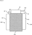
Fig. 17 is a side view illustrating a relationship between a coil sealing part, a primary-side sealing part, and a secondary-side sealing part, and a cooling body that can be used in a sixth embodiment of the present invention. -
Fig. 18 is a plan view illustrating an example of a disposition aspect of a primary-side sealing part and a secondary-side sealing part that can be used in an embodiment of the present invention. - In the present embodiment, "one side" means an upper side in
Fig. 3 , and "another side" means a lower side inFig. 3 . An upward or downward direction inFig. 3 is referred to as a "first direction", a leftward or rightward direction is referred to as a "second direction", and directions of front and reverse sides of paper are referred to as a "third direction". An in-plane direction including the second direction and the third direction is referred to as a "plane direction". - As illustrated in
Fig. 1 , an electronic device according to the present embodiment may have aprimary coil 10, asecondary coil 20 that is disposed to face theprimary coil 10, a primary-sideelectronic element 110 that is electrically connected to theprimary coil 10, and a secondary-sideelectronic element 210 that is electrically connected to thesecondary coil 20. As illustrated inFigs. 2 and3 , theprimary coil 10 may have a primary-sidefirst coil 10a that is provided on another side of thesecondary coil 20, and a primary-sidesecond coil 10b that is provided on one side of the primary-sidefirst coil 10a. As illustrated inFig. 4 , a connectingpart 19 connecting the primary-sidefirst coil 10a and the primary-sidesecond coil 10b may be provided and may pass through a space in a plane direction of the primary-sidesecond coil 10b. Theprimary coil 10 may be constituted of a lead frame. A thickness of thesecondary coil 20 may be greater than a thickness of theprimary coil 10. - As illustrated in
Fig. 6 , thesecondary coil 20 may be provided with a gap G without being wound one turn or more. Thesecondary coil 20 may have asecondary coil part 21 and a pair of secondary-side extension parts 70 that extend from both ends of thesecondary coil part 21 to be integrated with thesecondary coil part 21, and may be provided with the gap G between the pair of secondary-side extension parts 70. As illustrated inFigs. 3 and4 , the connectingpart 19 may pass through thesecondary coil 20 between both ends of thesecondary coil part 21 or between the pair of the secondary-side extension parts 70. The connectingpart 19 does not need to be completely parallel to the first direction, and may be inclined with respect to the first direction. An aspect of "extending along the first direction" also includes an aspect of extending to be inclined with respect to the first direction, as described above. Note that, in contrast to the aspect illustrated inFigs. 3 and4 , thesecondary coil 20 may be provided on the one side of the primary-sidesecond coil 10b, or thesecondary coil 20 may be provided on the other side of the primary-sidefirst coil 10a. - As illustrated in
Fig. 5 , acoil sealing part 50 sealing theprimary coil 10, thesecondary coil 20, and the connectingpart 19 and being made of sealing resin or the like may be provided. - A first
electronic module 100 that has the primary-sideelectronic element 110 and the primary-side sealing part 150 may be provided. As illustrated inFig. 1 , the firstelectronic module 100 may have a primary-side substrate 120, a plurality of primary-side conductor layers 130 that is provided on one surface of the primary-side substrate 120, and a primary-sideelectronic element 110 that is provided on one surface of the primary-side conductor layer 130. The primary-sideelectronic element 110, a surface on the one side of the primary-side substrate 120, and a surface on the one side of the primary-side conductor layer 130 may be sealed with the primary-side sealing part 150 (seeFig. 5 ). The primary-side sealing part 150 may be constituted of primary-side sealing resin. - As illustrated in
Fig. 7 , a primary-side first electrode (for example, a source electrode) 111 and a primary-side second electrode (for example, a gate electrode) 112 may be provided on one surface of the primary-sideelectronic element 110, and a primary-side third electrode (for example, a drain electrode) 113 may be provided on another surface of the primary-sideelectronic element 110. The primary-side first electrode 111 and the primary-side conductor layer 130 may be connected via a primary-side first connector 116 (seeFig. 1 ) and a conductive adhesive (not illustrated) such as solder. The primary-side second electrode 112 and the primary-side conductor layer 130 may be connected via a primary-side second connector 117 (seeFig. 1 ) and a conductive adhesive such as solder. The primary-side third electrode 113 and the primary-side conductor layer 130 may be connected via a conductive adhesive such as solder. Furthermore, as illustrated inFig. 8 , the primary-side first electrode 111 may be provided on one surface of the primary-sideelectronic element 110, and the primary-side second electrode 112 may be provided on another surface of the primary-sideelectronic element 110. - As illustrated in
Fig. 1 , a secondelectronic module 200 that has the secondary-sideelectronic element 210 and the secondary-side sealing part 250 (seeFig. 5 ) may be provided. As illustrated inFig. 1 , the secondelectronic module 200 may have a secondary-side substrate 220, a plurality of secondary-side conductor layers 230 that is provided on one surface of the secondary-side substrate 220, and a secondary-sideelectronic element 210 that is provided on one surface of the secondary-side conductor layer 230. The secondary-sideelectronic element 210, a surface on the one side of the secondary-side substrate 220, and a surface on the one side of the secondary-side conductor layer 230 may be sealed with the secondary-side sealing part 250 (seeFig. 5 ). The secondary-side sealing part 250 may be constituted of secondary-side sealing resin. The primary-side sealing resin and the secondary-side sealing resin may be constituted of the same resin material, or may be constituted of resin materials that are different from each other. - As illustrated in
Fig. 8 , a secondary-side first electrode 211 may be provided on one surface of the secondary-sideelectronic element 210, and a secondary-side second electrode 212 may be provided on another surface of the secondary-sideelectronic element 210. The secondary-side first electrode 211 and the secondary-side conductor layer 230 may be connected via a secondary-side first connector 216 (seeFig. 1 ) and a conductive adhesive such as solder. Furthermore, as illustrated inFig. 7 , the secondary-side first electrode (for example, a source electrode) 211 and the secondary-side second electrode (for example, a gate electrode) 212 may be provided on one surface of the secondary-sideelectronic element 210, and a secondary-side third electrode (for example, a drain electrode) 213 may be provided on another surface of the secondary-sideelectronic element 210. The secondary-side third electrode 213 and the secondary-side conductor layer 230 may be connected via a conductive adhesive such as solder. - The primary-side
first coil 10a and the primary-sidesecond coil 10b of theprimary coil 10 may have the same number of turns, or may have numbers of turns that are different from each other. As an example, each of the numbers of turns of the primary-sidefirst coil 10a and the primary-sidesecond coil 10b of theprimary coil 10 may be 4.5. The number of turns of thesecondary coil 20 may be 1, or may be 2 or more. - As illustrated in
Fig. 2 , theprimary coil 10 and a primary-side extension part 60 that extends to an inside of the primary-side sealing part 150 may be integrated. The primary-side extension part 60 may have a primary-sidefirst extension part 60a, and a primary-sidesecond extension part 60b that is located on the one side relative to the primary-sidefirst extension part 60a. The primary-sidefirst coil 10a and the primary-sidefirst extension part 60a may be integrated, and the primary-sidesecond coil 10b and the primary-sidesecond extension part 60b may be integrated. - As illustrated in
Fig. 9 , acore 500 such as an E-core that passes through theprimary coil 10 and thesecondary coil 20 may be provided. Thecore 500 may have aleg part 510, and theleg part 510 may be provided to pass through anopening part 51 that is provided in thecoil sealing part 50. Theleg part 510 of thecore 500 may be provided to abut onto an inner peripheral surface of thecoil sealing part 50. An outer peripheral part of thecore 500 may be provided to cover an outer periphery of thecoil sealing part 50. - Next, an example of operations or effects according to the present embodiment having the configuration described above is described. All of the aspects described in the "Effects" can be employed in the configuration described above.
- As illustrated in
Figs. 3 and4 , in a case where an aspect where the primary-sideelectronic element 110 that is electrically connected to theprimary coil 10 and the secondary-sideelectronic element 210 that is electrically connected to thesecondary coil 20 are provided, theprimary coil 10 has the primary-sidefirst coil 10a that is provided on the other side of thesecondary coil 20, and the primary-sidesecond coil 10b that is provided on the one side of thesecondary coil 20, and the connectingpart 19 connecting the primary-sidefirst coil 10a and the primary-sidesecond coil 10b is provided and passes through thesecondary coil 20 has been employed, a wiring length between the primary-sideelectronic element 110 and theprimary coil 10 can be reduced, a wiring length between the secondary-sideelectronic element 210 and thesecondary coil 20 can be reduced, and a size of an electronic device can be reduced. Furthermore, the primary-sidefirst coil 10a and the primary-sidesecond coil 10b can be provided to sandwich thesecondary coil 20, and therefore transmission efficiency in a transformer can also be enhanced. - In a case where an aspect in which the connecting
part 19 passes through thesecondary coil 20 between both ends of the secondary coil part 21 (see G1 ofFig. 6 ) or between the pair of secondary-side extension parts 70 (see G2 ofFig. 6 ) has been employed, there is an advantage in which the primary-sidefirst coil 10a and the primary-sidesecond coil 10b can be connected by using a connectingpart 19 having a short length. - As illustrated in
Fig. 5 , in a case where an aspect in which thecoil sealing part 50 with which theprimary coil 10 and thesecondary coil 20 are sealed and that is made of sealing resin is provided has been employed, an insulating sheet that has been conventionally used does not need to be provided, and as a result, a space that is inevitably formed between insulating sheets can be omitted. Therefore, thermal conductivity can be increased, and heat dissipation can be enhanced. - As illustrated in
Fig. 2 , in a case where an aspect in which the primary-sidefirst coil 10a of theprimary coil 10 and the primary-side extension part 60 that extends to the inside of the primary-side sealing part 150 are integrated has been employed, there is an advantage in which a member in which theprimary coil 10 and the primary-side extension part 60 are integrated can be easily manufactured, by forming theprimary coil 10 and the primary-side extension part 60 in a member such as a lead frame and removing an unnecessary portion. - As illustrated in
Fig. 1 , in a case where an aspect in which thesecondary coil 20 and the secondary-side extension parts 70 that extend to the inside of the secondary-side sealing part 250 are integrated has been employed, a member in which thesecondary coil 20 and the secondary-side extension parts 70 are integrated can be easily manufactured, by forming thesecondary coil 20 and the secondary-side extension parts 70 in a member such as a lead frame and removing an unnecessary portion. - As illustrated in
Fig. 10 , a cooling body such as a heat sink may be provided on another surface (a back surface) of thecoil sealing part 50, another surface (a back surface) of the primary-side sealing part 150, and another surface (a back surface) of the secondary-side sealing part 250. In a case where such an aspect has been employed, there is an advantage in which thecoil sealing part 50, the primary-side sealing part 150, and the secondary-side sealing part 250 can be cooled down by the cooling body. - Next, a second embodiment of the present invention is described.
- In the present embodiment, as illustrated in
Fig. 11 , the primary-sideelectronic element 110 has a primary-side firstelectronic element 110a, and a primary-side secondelectronic element 110b that is provided on the one side relative to the primary-side firstelectronic element 110a. The primary-side firstelectronic element 110a may be provided on the primary-sidefirst extension part 60a that extends from the primary-sidefirst coil 10a, and may be electrically connected to the primary-sidefirst coil 10a. The primary-side secondelectronic element 110b may be provided on the primary-sidesecond extension part 60b that extends from the primary-sidesecond coil 10b, and may be electrically connected to the primary-sidesecond coil 10b. The other configuration is similar to a configuration in the first embodiment, and all of the aspects described in the first embodiment can be employed. The members described in the first embodiment are described by using the same reference signs. - The primary-side
electronic element 110 may be sealed with the primary-side sealing part 150. The secondary-sideelectronic element 210 may be sealed with the secondary-side sealing part 250. - As described above, an aspect in which the primary-side first
electronic element 110a is provided on the primary-sidefirst extension part 60a that extends from the primary-sidefirst coil 10a to an outside of thecoil sealing part 50 may be employed. In this case, wiring length can be further reduced, and the size of the electronic device can be reduced. Similarly, an aspect in which the primary-side secondelectronic element 110b is provided on the primary-sidesecond extension part 60b that extends from the primary-sidesecond coil 10b to the outside of thecoil sealing part 50 may be employed. In this case, similarly, wiring length can be further reduced, and the size of the electronic device can be reduced. The primary-side firstelectronic element 110a may be provided on the primary-sidefirst extension part 60a via a conductive adhesive such as solder, and the primary-side secondelectronic element 110b may be provided on the primary-sidesecond extension part 60b via a conductive adhesive such as solder. - Furthermore, the primary-side
first extension part 60a and the primary-sidesecond extension part 60b are provided on the other side and the one side of the secondary-side coil 20, and the primary-sidefirst extension part 60a and the primary-sidesecond extension part 60b are disposed to be spaced apart from each other in the first direction. This can suppress an influence of noise or the like that occurs from the primary-side firstelectronic element 110a that is provided on one surface of the primary-sidefirst extension part 60a on the primary-side secondelectronic element 110b that is provided on one surface of the primary-sidesecond extension part 60b, or in contrast, an influence of noise or the like that occurs from the primary-side secondelectronic element 110b on the primary-side firstelectronic element 110a. Furthermore, as illustrated inFig. 11 , in a case where the primary-sidefirst extension part 60a and the primary-sidesecond extension part 60b are located on opposite sides across the connectingpart 19, when viewed from the second direction, there is further an advantage in which the primary-sidefirst extension part 60a and the primary-sidesecond extension part 60b can be disposed to be spaced apart from each other. - As illustrated in
Fig. 12 , the primary-sideelectronic element 110 may be provided on each of the one side and the other side of the primary-side extension part 60. A primary-side connecting body 190 that connects a plurality of primary-sideelectronic elements 110 that is provided on the one side of the primary-side extension part 60 may be provided. As an example, a primary-side first electrode (for example, a source electrode) 111 (seeFig. 7 ) of a primary-sideelectronic element 110 that is located on the other side of the primary-side extension part 60 and a primary-side third electrode (for example, a drain electrode) 113 (seeFig. 7 ) of a primary-sideelectronic element 110 that is located on the one side of the primary-side extension part 60 may be electrically connected by the primary-side extension part 60 (see two primary-sideelectronic elements 110 that are located on a left-hand side inFig. 12 ). Furthermore, primary-side first electrodes (for example, source electrodes) 111 (seeFig. 7 ) of a plurality of primary-sideelectronic elements 110 that is located on the one side of the primary-side extension part 60 may be electrically connected by the primary-side connecting body 190 (see a primary-sideelectronic element 110 that is located on a leftmost side and a primary-sideelectronic element 110 that is located on a rightmost side inFig. 12 ). - Next, a third embodiment of the present invention is described.
- In the present embodiment, as illustrated in
Fig. 13 , an aspect in which the secondary-sideelectronic element 210 is provided on the secondary-side extension part 70 that extends from thesecondary coil 20 to the outside of thecoil sealing part 50 is employed. The other configuration is similar to a configuration in the first embodiment or the second embodiment, and all of the aspects described in each of the embodiments described above can be employed. The members described in each of the embodiments described above are described by using the same reference signs. - In a case where an aspect in which the secondary-side
electronic element 210 is provided on the secondary-side extension part 70 that extends from thesecondary coil 20 to the outside of thecoil sealing part 50, as in the present embodiment, has been employed, wiring length can be further reduced, and the size of the electronic device can be reduced. The secondary-sideelectronic element 210 may be provided on the secondary-side extension part 70 via a conductive adhesive such as solder. As illustrated inFig. 13 , a widthwise length of abase end 71 of the secondary-side extension part 70 may be longer in the third direction than a widthwise length of the secondary-sideelectronic element 210, and the secondary-sideelectronic element 210 may be placed on thebase end 71. - As illustrated in
Fig. 14 , the secondary-sideelectronic element 210 may be provided on each of the one side and the other side of the secondary-side extension part 70. A secondary-side connecting body 290 that connects a plurality of secondary-sideelectronic elements 210 that is provided on the one side of the secondary-side extension part 70 may be provided. As an example, a secondary-side first electrode (for example, a source electrode) 211 (seeFig. 7 ) of a secondary-sideelectronic element 210 that is located on the other side of the secondary-side extension part 70 and a secondary-side third electrode (for example, a drain electrode) 213 (seeFig. 7 ) of a secondary-sideelectronic element 210 that is located on the one side of the secondary-side extension part 70 may be electrically connected by the secondary-side extension part 70 (see two secondary-sideelectronic elements 210 that are disposed in an upward or downward direction inFig. 14 ). Furthermore, secondary-side first electrodes (for example, source electrodes) 211 (seeFig. 7 ) of a plurality of secondary-sideelectronic elements 210 that is located on the one side of the secondary-side extension part 70 may be electrically connected by the secondary-side connecting body 290 (see two secondary-sideelectronic elements 210 that are disposed on left-hand and right-hand sides on an upper side inFig. 14 ). - Next, a fourth embodiment of the present invention is described.
- As illustrated in
Fig. 15 , in the present embodiment, an aspect in which a firstbent part 310 is provided in the primary-side extension part 60 between thecoil sealing part 50 and the primary-side sealing part 150 is employed. The other configuration is similar to configurations in the first to third embodiments, and all of the aspects described in each of the embodiments described above can be employed. The members described in each of the embodiments described above are described by using the same reference signs. - According to the present embodiment, the
coil sealing part 50 and the secondary-side sealing part 250 can be disposed along a plane direction, and the primary-side sealing part 150 can be disposed along a direction that is bent by a predetermined angle (for example, 60 degrees, 90 degrees, 120 degrees, or the like) with respect to the plane direction. Therefore, a size in a certain plane direction can be reduced. - Furthermore, such bending enables a reduction in an influence of noise or the like generated in the primary-side
electronic element 110 sealed with the primary-side sealing part 150 on the secondary-sideelectronic element 210 sealed with the secondary-side sealing part 250, and also enables a reduction in an influence of noise or the like generated in the secondary-sideelectronic element 210 on the secondary-sideelectronic element 210 sealed with the primary-side sealing part 150. - In the present embodiment, similarly, the cooling
body 350 such as a heat sink may be provided on the back surface of thecoil sealing part 50, the back surface of the primary-side sealing part 150, and the back surface of the secondary-side sealing part 250. In a case where such an aspect has been employed, there is an advantage in which thecoil sealing part 50, the primary-side sealing part 150, and the secondary-side sealing part 250 can be cooled down by the coolingbody 350. - Next, a fifth embodiment of the present invention is described.
- As illustrated in
Fig. 16 , in the present embodiment, an aspect in which a secondbent part 320 is provided in the secondary-side extension part 70 between thecoil sealing part 50 and the secondary-side sealing part 250 is employed. The other configuration is similar to configurations in the first to third embodiments, and all of the aspects described in each of the embodiments described above can be employed. The members described in each of the embodiments described above are described by using the same reference signs. - According to the present aspect, the
coil sealing part 50 and the primary-side sealing part 150 can be disposed along a plane direction, and the secondary-side sealing part 250 can be disposed along a direction that is bent by a predetermined angle (for example, 60 degrees, 90 degrees, 120 degrees, or the like) with respect to the plane direction. Therefore, a size in a certain plane direction can be reduced. - Furthermore, such bending enables a reduction in an influence of noise or the like generated in the primary-side
electronic element 110 sealed with the primary-side sealing part 150 on the secondary-sideelectronic element 210 sealed with the secondary-side sealing part 250, and also enables a reduction in an influence of noise or the like generated in the secondary-sideelectronic element 210 on the secondary-sideelectronic element 210 sealed with the primary-side sealing part 150. - In the present embodiment, similarly, the cooling
body 350 such as a heat sink may be provided on the back surface of thecoil sealing part 50, the back surface of the primary-side sealing part 150, and the back surface of the secondary-side sealing part 250. In a case where such an aspect has been employed, there is an advantage in which thecoil sealing part 50, the primary-side sealing part 150, and the secondary-side sealing part 250 can be cooled down by the coolingbody 350. - Next, a sixth embodiment of the present invention is described.
- As illustrated in
Fig. 17 , in the present embodiment, an aspect in which the firstbent part 310 is provided in the primary-side extension part 60 between thecoil sealing part 50 and the primary-side sealing part 150 and the secondbent part 320 is provided in the s secondary-side extension part 70 between thecoil sealing part 50 and the secondary-side sealing part 250 is employed. The other configuration is similar to a configuration in the first to third embodiments, and all of the aspects described in each of the embodiments described above can be employed. The members described in each of the embodiments described above are described by using the same reference signs. - According to the present embodiment, the
coil sealing part 50, the primary-side sealing part 150, and the secondary-side sealing part 250 can be respectively disposed along plane directions that are different from each other. Furthermore, the primary-side sealing part 150 and the secondary-side sealing part 250 can also be disposed in such a way that respective back surfaces face each other. Thecoil sealing part 50 and the primary-side sealing part 150 may be disposed to be bent by a first angle (for example, 60 degrees, 90 degrees, 120 degrees, or the like) with respect to each other, and thecoil sealing part 50 and the secondary-side sealing part 250 may be disposed to be bent by a second angle (for example, 60 degrees, 90 degrees, 120 degrees, or the like) with respect to each other. - In the present embodiment, similarly, the cooling
body 350 such as a heat sink may be provided on the back surface of thecoil sealing part 50, the back surface of the primary-side sealing part 150, and the back surface of the secondary-side sealing part 250. In a case where such an aspect has been employed, there is an advantage in which thecoil sealing part 50, the primary-side sealing part 150, and the secondary-side sealing part 250 can be cooled down by the coolingbody 350. As an example, in a case where, for example, an aspect in which thecoil sealing part 50 and the primary-side sealing part 150 are disposed to be bent by 90 degrees with respect to each other and thecoil sealing part 50 and the secondary-side sealing part 250 are disposed to be bent by 90 degrees with respect to each other has been employed, disposition can be performed in such a way that the back surface of thecoil sealing part 50, the back surface of the primary-side sealing part 150, and the back surface of the secondary-side sealing part 250 respectively abut onto three surfaces of thecooling body 350 that is made of a heat sink or the like, and there is an advantage in which a high cooling effect can be expected. - The primary-
side terminal 60 and the secondary-side terminal 70 do not need to be provided linearly. For example, the primary-side terminal 60 and the secondary-side terminal 70 may be provided to be orthogonal to each other in a plane direction, or may be provided to cross each other at an angle that is different from 90 degrees in the plane direction.Fig. 18 illustrates an aspect in which the primary-side terminal 60 and the secondary-side terminal 70 are orthogonal to each other in the plane direction. As described above, according to the present embodiment, the primary-side sealing part 150 and the secondary-side sealing part 250 can be disposed in any direction of the plane direction, and can be bent by using the firstbent part 310 and the secondbent part 320. - The description of each embodiment and the disclosure of the drawings described above are merely examples for explaining the invention described in the claims, and the invention described in the claims is not limited by the description of the embodiment or the disclosure of the drawings described above. In addition, the recitation of the claims at the original application is merely an example, and the description of the claims can be appropriately changed based on the description of the specification, the drawings, and the like.
-
- 10
- Primary coil
- 10a
- Primary-side first coil
- 10b
- Primary-side second coil
- 19
- Connecting part
- 20
- Secondary coil
- 21
- Secondary coil part
- 50
- Coil sealing part
- 60
- Primary-side terminal
- 70
- Secondary-side terminal
- 110
- Primary-side electronic element
- 110a
- Primary-side first electronic element
- 110b
- Primary-side second electronic element
- 150
- Primary-side sealing part
- 210
- Secondary-side electronic element
Claims (8)
- An electronic device comprising:a primary coil;a secondary coil disposed to face the primary coil;a primary-side electronic element electrically connected to the primary coil; anda secondary-side electronic element electrically connected to the secondary coil, whereinthe primary coil has a primary-side first coil that is provided on another side of the secondary coil, and a primary-side second coil that is provided on one side of the primary-side first coil, anda connecting part connecting the primary-side first coil and the primary-side second coil is provided and passes through a space of the secondary coil.
- The electronic device according to claim 1, wherein
the secondary coil has a secondary coil part and a pair of secondary-side extension parts that extend from both ends of the secondary coil part, and
the connecting part passes through the space of the secondary coil between the both ends of the secondary coil part or between the pair of the secondary-side extension parts. - The electronic device according to claim 1 further comprising a coil sealing part sealing the primary coil, the secondary coil, and the connecting part.
- The electronic device according to claim 1, wherein
the primary-side electronic element has a primary-side first electronic element and a primary-side second electronic element provided on one side relative to the primary-side first electronic element,
the primary-side first electronic element is electrically connected to the primary-side first coil, and
the primary-side second electronic element is electrically connected to the primary-side second coil. - The electronic device according to claim 4, wherein
the primary-side first electronic element is provided on a primary-side first extension part that extends from the primary-side first coil, or the primary-side second electronic element is provided on a primary-side second extension part that extends from the primary-side second coil. - The electronic device according to claim 1 further comprising a primary-side sealing part sealing the primary-side electronic element, or a secondary-side sealing part sealing the secondary-side electronic element.
- The electronic device according to claim 1 further comprising a first electronic module having the primary-side electronic element, a primary-side substrate on which the primary-side electronic element is provided and a primary-side sealing part sealing the primary-side electronic element, or a second electronic module having the secondary-side electronic element, a secondary-side substrate on which the secondary-side electronic element is provided and a secondary-side sealing part sealing the secondary-side electronic element.
- The electronic device according to claim 1, wherein
the primary-side first coil or the primary-side second coil is made from a lead frame.
Applications Claiming Priority (1)
| Application Number | Priority Date | Filing Date | Title |
|---|---|---|---|
| PCT/JP2018/024766 WO2020003483A1 (en) | 2018-06-29 | 2018-06-29 | Electronic device |
Publications (2)
| Publication Number | Publication Date |
|---|---|
| EP3817018A1 true EP3817018A1 (en) | 2021-05-05 |
| EP3817018A4 EP3817018A4 (en) | 2022-06-01 |
Family
ID=68986806
Family Applications (1)
| Application Number | Title | Priority Date | Filing Date |
|---|---|---|---|
| EP18924813.1A Pending EP3817018A4 (en) | 2018-06-29 | 2018-06-29 | Electronic device |
Country Status (5)
| Country | Link |
|---|---|
| US (1) | US11967451B2 (en) |
| EP (1) | EP3817018A4 (en) |
| JP (1) | JP7149330B2 (en) |
| CN (1) | CN112368794B (en) |
| WO (1) | WO2020003483A1 (en) |
Family Cites Families (14)
| Publication number | Priority date | Publication date | Assignee | Title |
|---|---|---|---|---|
| JP4066840B2 (en) * | 2003-02-21 | 2008-03-26 | 株式会社デンソー | Transformer and its assembly method |
| NO320550B1 (en) | 2004-06-07 | 2005-12-19 | Applied Plasma Physics Asa | Device by planar high voltage transformer |
| US8502632B2 (en) | 2008-04-24 | 2013-08-06 | Panasonic Corporation | Transformer, power converter, lighting device, lighting device for vehicle, and vehicle using the same |
| US7969002B2 (en) * | 2008-10-29 | 2011-06-28 | Maxim Integrated Products, Inc. | Integrated circuit packages incorporating an inductor and methods |
| JP2010123898A (en) | 2008-11-21 | 2010-06-03 | Toyota Motor Corp | Semiconductor device |
| US10111333B2 (en) * | 2010-03-16 | 2018-10-23 | Intersil Americas Inc. | Molded power-supply module with bridge inductor over other components |
| JP2012104724A (en) * | 2010-11-12 | 2012-05-31 | Panasonic Corp | Inductor component |
| JP2012231616A (en) * | 2011-04-27 | 2012-11-22 | Diamond Electric Mfg Co Ltd | On-vehicle power conversion device |
| JP6317948B2 (en) * | 2014-02-24 | 2018-04-25 | 新電元工業株式会社 | Transformer coil connection structure and transformer |
| JP2017038053A (en) | 2015-08-06 | 2017-02-16 | 日本精工株式会社 | Semiconductor module, drive device including the same, electric power steering device, and vehicle |
| CN207381409U (en) * | 2017-08-14 | 2018-05-18 | 深圳市芯电元科技有限公司 | It is inverted the power MOSFET of gate structure |
| WO2020003482A1 (en) * | 2018-06-29 | 2020-01-02 | 新電元工業株式会社 | Electronic device |
| US12051536B2 (en) * | 2018-06-29 | 2024-07-30 | Shindengen Electric Manufacturing Co., Ltd. | Electronic device |
| CN112292740B (en) * | 2018-06-29 | 2024-05-28 | 新电元工业株式会社 | Magnetic components |
-
2018
- 2018-06-29 WO PCT/JP2018/024766 patent/WO2020003483A1/en not_active Ceased
- 2018-06-29 JP JP2020526844A patent/JP7149330B2/en active Active
- 2018-06-29 EP EP18924813.1A patent/EP3817018A4/en active Pending
- 2018-06-29 CN CN201880095120.0A patent/CN112368794B/en active Active
- 2018-06-29 US US17/255,951 patent/US11967451B2/en active Active
Also Published As
| Publication number | Publication date |
|---|---|
| WO2020003483A1 (en) | 2020-01-02 |
| US11967451B2 (en) | 2024-04-23 |
| EP3817018A4 (en) | 2022-06-01 |
| CN112368794B (en) | 2024-05-28 |
| JPWO2020003483A1 (en) | 2021-08-12 |
| CN112368794A (en) | 2021-02-12 |
| US20210272746A1 (en) | 2021-09-02 |
| JP7149330B2 (en) | 2022-10-06 |
Similar Documents
| Publication | Publication Date | Title |
|---|---|---|
| JP5144210B2 (en) | Semiconductor device | |
| CN208352514U (en) | Anneta module and electronic device with the Anneta module | |
| US12051536B2 (en) | Electronic device | |
| CN116052974A (en) | Coil component | |
| US10062633B2 (en) | Substrate unit | |
| US12272489B2 (en) | Electronic device | |
| US12148562B2 (en) | Magnetic component | |
| US11967451B2 (en) | Electronic device | |
| JP2008078178A (en) | Inductor | |
| NL2018997A (en) | Coil structure and magnetic component | |
| US12417875B2 (en) | Electronic device | |
| JP4776185B2 (en) | Coil parts | |
| JP2021034602A (en) | Inductor component | |
| JP6325757B1 (en) | Electronic equipment | |
| JP7632151B2 (en) | Electronics | |
| JP2017055039A (en) | Coil parts |
Legal Events
| Date | Code | Title | Description |
|---|---|---|---|
| STAA | Information on the status of an ep patent application or granted ep patent |
Free format text: STATUS: THE INTERNATIONAL PUBLICATION HAS BEEN MADE |
|
| PUAI | Public reference made under article 153(3) epc to a published international application that has entered the european phase |
Free format text: ORIGINAL CODE: 0009012 |
|
| STAA | Information on the status of an ep patent application or granted ep patent |
Free format text: STATUS: REQUEST FOR EXAMINATION WAS MADE |
|
| 17P | Request for examination filed |
Effective date: 20210122 |
|
| AK | Designated contracting states |
Kind code of ref document: A1 Designated state(s): AL AT BE BG CH CY CZ DE DK EE ES FI FR GB GR HR HU IE IS IT LI LT LU LV MC MK MT NL NO PL PT RO RS SE SI SK SM TR |
|
| DAV | Request for validation of the european patent (deleted) | ||
| DAX | Request for extension of the european patent (deleted) | ||
| RIC1 | Information provided on ipc code assigned before grant |
Ipc: H01F 27/28 20060101ALI20220118BHEP Ipc: H01F 30/10 20060101AFI20220118BHEP |
|
| A4 | Supplementary search report drawn up and despatched |
Effective date: 20220429 |
|
| RIC1 | Information provided on ipc code assigned before grant |
Ipc: H01F 27/28 20060101ALI20220422BHEP Ipc: H01F 30/10 20060101AFI20220422BHEP |
|
| STAA | Information on the status of an ep patent application or granted ep patent |
Free format text: STATUS: EXAMINATION IS IN PROGRESS |
|
| 17Q | First examination report despatched |
Effective date: 20240925 |