EP3800662A1 - Security chip, preparation method for security chip, and electronic device - Google Patents
Security chip, preparation method for security chip, and electronic device Download PDFInfo
- Publication number
- EP3800662A1 EP3800662A1 EP19920630.1A EP19920630A EP3800662A1 EP 3800662 A1 EP3800662 A1 EP 3800662A1 EP 19920630 A EP19920630 A EP 19920630A EP 3800662 A1 EP3800662 A1 EP 3800662A1
- Authority
- EP
- European Patent Office
- Prior art keywords
- dielectric layer
- security chip
- layer
- spike
- light
- Prior art date
- Legal status (The legal status is an assumption and is not a legal conclusion. Google has not performed a legal analysis and makes no representation as to the accuracy of the status listed.)
- Granted
Links
Images

Classifications
-
- H—ELECTRICITY
- H04—ELECTRIC COMMUNICATION TECHNIQUE
- H04L—TRANSMISSION OF DIGITAL INFORMATION, e.g. TELEGRAPHIC COMMUNICATION
- H04L9/00—Cryptographic mechanisms or cryptographic arrangements for secret or secure communications; Network security protocols
- H04L9/002—Countermeasures against attacks on cryptographic mechanisms
- H04L9/004—Countermeasures against attacks on cryptographic mechanisms for fault attacks
-
- G—PHYSICS
- G07—CHECKING-DEVICES
- G07F—COIN-FREED OR LIKE APPARATUS
- G07F7/00—Mechanisms actuated by objects other than coins to free or to actuate vending, hiring, coin or paper currency dispensing or refunding apparatus
- G07F7/08—Mechanisms actuated by objects other than coins to free or to actuate vending, hiring, coin or paper currency dispensing or refunding apparatus by coded identity card or credit card or other personal identification means
- G07F7/0806—Details of the card
- G07F7/0813—Specific details related to card security
- G07F7/082—Features insuring the integrity of the data on or in the card
-
- G—PHYSICS
- G07—CHECKING-DEVICES
- G07F—COIN-FREED OR LIKE APPARATUS
- G07F7/00—Mechanisms actuated by objects other than coins to free or to actuate vending, hiring, coin or paper currency dispensing or refunding apparatus
- G07F7/08—Mechanisms actuated by objects other than coins to free or to actuate vending, hiring, coin or paper currency dispensing or refunding apparatus by coded identity card or credit card or other personal identification means
- G07F7/0806—Details of the card
- G07F7/0833—Card having specific functional components
-
- G—PHYSICS
- G09—EDUCATION; CRYPTOGRAPHY; DISPLAY; ADVERTISING; SEALS
- G09C—CIPHERING OR DECIPHERING APPARATUS FOR CRYPTOGRAPHIC OR OTHER PURPOSES INVOLVING THE NEED FOR SECRECY
- G09C1/00—Apparatus or methods whereby a given sequence of signs, e.g. an intelligible text, is transformed into an unintelligible sequence of signs by transposing the signs or groups of signs or by replacing them by others according to a predetermined system
-
- H—ELECTRICITY
- H10—SEMICONDUCTOR DEVICES; ELECTRIC SOLID-STATE DEVICES NOT OTHERWISE PROVIDED FOR
- H10W—GENERIC PACKAGES, INTERCONNECTIONS, CONNECTORS OR OTHER CONSTRUCTIONAL DETAILS OF DEVICES COVERED BY CLASS H10
- H10W42/00—Arrangements for protection of devices
- H10W42/20—Arrangements for protection of devices protecting against electromagnetic or particle radiation, e.g. light, X-rays, gamma-rays or electrons
-
- H—ELECTRICITY
- H10—SEMICONDUCTOR DEVICES; ELECTRIC SOLID-STATE DEVICES NOT OTHERWISE PROVIDED FOR
- H10W—GENERIC PACKAGES, INTERCONNECTIONS, CONNECTORS OR OTHER CONSTRUCTIONAL DETAILS OF DEVICES COVERED BY CLASS H10
- H10W42/00—Arrangements for protection of devices
- H10W42/40—Arrangements for protection of devices protecting against tampering, e.g. unauthorised inspection or reverse engineering
-
- H—ELECTRICITY
- H10—SEMICONDUCTOR DEVICES; ELECTRIC SOLID-STATE DEVICES NOT OTHERWISE PROVIDED FOR
- H10W—GENERIC PACKAGES, INTERCONNECTIONS, CONNECTORS OR OTHER CONSTRUCTIONAL DETAILS OF DEVICES COVERED BY CLASS H10
- H10W70/00—Package substrates; Interposers; Redistribution layers [RDL]
- H10W70/60—Insulating or insulated package substrates; Interposers; Redistribution layers
-
- H—ELECTRICITY
- H10—SEMICONDUCTOR DEVICES; ELECTRIC SOLID-STATE DEVICES NOT OTHERWISE PROVIDED FOR
- H10W—GENERIC PACKAGES, INTERCONNECTIONS, CONNECTORS OR OTHER CONSTRUCTIONAL DETAILS OF DEVICES COVERED BY CLASS H10
- H10W99/00—Subject matter not provided for in other groups of this subclass
Definitions
- Embodiments of the present application relate to the field of security chips, and more particularly, to a security chip, a security chip production method and an electronic device.
- a security chip is a special chip that can execute complex encryption and decryption algorithms.
- a secret key is stored in a special storage area of the security chip, and an attacker usually obtains the secret key by means of bypass attack, fault injection, and hardware Trojan horse.
- Laser fault injection is a very threatening attack method. Because there is a metal layer on the front of the security chip, it has a reflection effect on a laser. An attacker usually uses an infrared laser to illuminate a specific circuit on the front of the chip through the back of the security chip, and uses photocurrent generated by interaction between the laser and silicon to make the security chip output wrong results. Finally, the attacker can obtain the secret key by collecting errors with certain characteristics that occur at a specific time and at a specific location, and performing comparison and analysis with correct encryption results.
- a photosensitive module is usually provided in a security chip.
- an instruction command is issued to instruct erasure of a secret key stored in the security chip.
- the photosensitive module needs to occupy an additional chip area, which increases chip costs.
- a security chip a security chip production method and an electronic device, which can ensure that a laser attack is prevented in a case that an additional chip area is not occupied.
- a security chip including:
- the vertical light incident in a vertical direction with respect to a lower surface of the first dielectric layer when the roughness of the upper surface of the first dielectric layer is greater than or equal to the preset threshold, the vertical light can reach an interface between the first dielectric layer and the second dielectric layer, which increases its angle of incidence so that the angle of incidence is greater than a critical angle to meet conditions for total reflection; and the vertical light entering the first dielectric layer through total reflection can effectively reduce intensity of refracted light entering the second dielectric layer, so that most of the light cannot reach a logic or storage area on the front of the security chip, thereby achieving the purpose of resisting a laser attack.
- oblique light incident in an oblique direction with respect to the lower surface of the first dielectric layer when the roughness of the upper surface of the first dielectric layer is greater than or equal to the preset threshold, light receiving area of the second dielectric layer for the oblique light can be reduced, which further reduces the amount of refracted light entering the second dielectric layer, thereby achieving the purpose of resisting a laser attack.
- a propagation path of the oblique light in the first dielectric layer is longer, which further increases the loss in the process that the oblique light reaches the first dielectric layer and the second dielectric layer, and further reduces intensity of the light entering the second dielectric layer.
- the upper surface of the first dielectric layer whose roughness is greater than the preset threshold can scatter the light, so that a laser cannot be concentrated to a specific area, thereby further reducing intensity of refracted light entering the second dielectric layer.
- light incident from the lower surface of the first dielectric layer is able to be totally reflected or scattered by the upper surface of the first dielectric layer, thereby reducing intensity of light reaching the logic or storage area on the front of the security chip, thereby achieving the purpose of resisting a laser attack.
- the semiconductor chip on a substrate formed by the first dielectric layer and the second dielectric layer, not only a laser attack can be ensured to be prevented in a case that an additional chip area is not occupied, but also a process flow is relatively simple and does not affect a processing method of the chip, which is convenient for mass production.
- the preset threshold is 20 nm.
- the upper surface of the first dielectric layer is provided with a spike-like structure or a hole-like structure.
- the spike-like structure is formed by an irregularly-sized pyramidal protrusion or inverted pyramidal pit.
- an oblique surface of the pyramidal protrusion and a bottom surface of the first dielectric layer form an angle of 54.7 degrees.
- a material of the first dielectric layer is silicon (Si), and a material of the second dielectric layer is silicon dioxide (SiO 2 ).
- An angled Si/SiO 2 interface is formed inside the substrate.
- the incident light is totally reflected at the Si/SiO 2 interface, so that most of the laser cannot reach the logic or storage area on the front of the security chip, thereby achieving the purpose of resisting a laser attack.
- the semiconductor chip includes:
- an electronic device including the security chip in the first aspect and any possible embodiment of the first aspect.
- a method for producing a security chip including:
- the preset threshold is 20 nm.
- the method before the forming the second dielectric layer on the upper surface of the first dielectric layer, the method further includes: forming the upper surface of the first dielectric layer that is provided with a spike-like structure or a hole-like structure.
- the spike-like structure is formed by an irregularly-sized pyramidal protrusion or pyramidal pit.
- an oblique surface of the pyramidal protrusion and a bottom surface of the first dielectric layer form an angle of 54.7 degrees.
- the forming the upper surface of the first dielectric layer that is provided with the spike-like structure or the hole-like structure includes: forming the upper surface of the first dielectric layer that is provided with the spike-like structure or the hole-like structure by at least one of the following processes: a physical mechanical grinding process, a dry etching process, a metal assisted corrosion process, and an electrochemical corrosion process.
- the forming the upper surface of the first dielectric layer that is provided with the spike-like structure or the hole-like structure includes:
- the corrosive agent includes at least one of the following: a sodium hydroxide (NaOH) solution, a potassium hydroxide (KOH) solution, a tetramethylammonium hydroxide (TMAH) solution, and a sodium silicate (Na 2 SiO 3 ) solution.
- the heating the corrosive agent includes: heating the corrosive agent to a temperature above 80°C and performing corrosion for more than 25 minutes.
- a concentration of the corrosive agent is greater than or equal to 8 wt%.
- the forming the second dielectric layer on the upper surface of the first dielectric layer includes: forming the second dielectric layer on the upper surface of the first dielectric layer by a deposition process.
- the method before the producing the semiconductor chip on the second dielectric layer, the method further includes: forming a flat upper surface of the second dielectric layer by a planarization process.
- the producing the semiconductor chip on the second dielectric layer includes:
- the method before the producing the device layer on the substrate, the method further includes: thinning the substrate.
- the thinning the substrate includes: thinning the substrate to 10 um or less.
- a security chip including the security chip produced in the method in the third aspect and any possible embodiment of the third aspect.
- the embodiments of the present application are suitable for manufacturing various chips, especially a special chip or a security chip that can execute complex encryption and decryption algorithms.
- the security chip may be a biochip (such as a fingerprint sensor chip), a chip provided with a circuit (such as a processor), various types of chips in the Internet of Things field, and so on.
- the security chip may include an element such as a transistor, a resistor, a capacitor, and an inductor, and a wiring device or component.
- the security chip may be a miniature electronic device or component carrying an integrated circuit (integrated circuit). This is not specifically limited by the present application.
- the technical solutions in the embodiments of the present application may be applied to various electronic devices, for example, portable or mobile computing devices such as a smart phone, a notebook computer, a tablet computer and a game device, and other electronic devices such as an electronic database, an automobile and an automated teller machine (Automated Teller Machine, ATM), which is not limited in the embodiments of the present application.
- portable or mobile computing devices such as a smart phone, a notebook computer, a tablet computer and a game device
- other electronic devices such as an electronic database, an automobile and an automated teller machine (Automated Teller Machine, ATM), which is not limited in the embodiments of the present application.
- ATM Automate Teller Machine
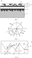
- FIG. 1 is a schematic structural diagram of a security chip according to an embodiment of the present application.
- a security chip 10 includes a first dielectric layer 11, a second dielectric layer 12 and a semiconductor chip 13.
- the second dielectric layer 12 is disposed on the first dielectric layer 11, and the 110 is disposed on the second dielectric layer 12.
- the semiconductor chip 13 can be etched and wired on a semiconductor sheet to produce a semiconductor device that can realize a certain function.
- the semiconductor chip 13 may include a substrate 131, a device layer 132 disposed on the substrate 131, and an interconnection layer 133 disposed on the device layer 132.
- the interconnection layer 132 may be realized by disposing a metal layer 134 in a dielectric layer, which is not limited in the present application.
- the first dielectric layer 11 may be an optically denser medium relative to the second dielectric layer 12 (that is, a refractive index of the first dielectric layer 11 is greater than a refractive index of the second dielectric layer 12).
- the second dielectric layer 12 may be an optically thinner medium relative to the first dielectric layer 11 (that is, the refractive index of the second dielectric layer 12 is smaller than the refractive index of the first dielectric layer 11).
- a roughness of an upper surface of the first dielectric layer 11 is greater than or equal to a preset threshold, so that light entering the second dielectric layer 12 vertically from the first dielectric layer 11 is able to be totally reflected and/or scattered.
- the preset threshold may be 20 nm.
- Total reflection also known as total internal reflection, refers to a phenomenon that when light is transmitted from an optically denser medium (that is, a refractive index of light in this medium is great) to an interface of an optically thinner medium (that is, a refractive index of light in this medium is small), it is all reflected back into the original medium.
- FIG. 2 is a schematic principle diagram of light propagating in two media according to an embodiment of the present application.
- light enters from an optically denser medium 18 with a higher refractive index n 1 into an optically thinner medium 19 with a lower refractive index n 2 .
- an angle of incidence ⁇ 1 of first light 181 is smaller than a critical angle ⁇ c
- the light 181 is refracted toward the optically thinner medium 19 to generate refracted light 182, while reflected toward the optically denser medium 18 to generate reflected light 183
- an angle of incidence ⁇ 2 of second light 191 is greater than or equal to the critical angle ⁇ c
- light refracted toward the optically thinner medium 19 disappears, and the second light 191 is only reflected toward the optically denser medium 18 to form reflected light 192, that is, the second light 191 is totally reflected, which is also called total internal reflection.
- the critical angle ⁇ c can also be considered as an angle of incidence when an angle of refraction is 90 degrees.
- the optically denser medium 18 and the optically thinner medium 19 are relatively speaking. When two substances are compared, one with a smaller refractive index is an optically thinner medium, and one with a greater refractive index is an optically denser medium. For example, if a refractive index of air is about 1, a refractive index of water is about 1.33, and a refractive index of glass is about 1.5, water is an optically denser medium relative to air, and water is an optically thinner medium relative to glass.
- the present application does not limit the specific materials of the first dielectric layer 11 and the second dielectric layer 12, as long as it is ensured that the refractive index of the first dielectric layer 11 is greater than the refractive index of the second dielectric layer 12.
- a propagation path of the oblique light in the first dielectric layer 11 is longer, which further increases the loss in the process that the oblique light reaches the first dielectric layer 11 and the second dielectric layer 12, and further reduces intensity of the light entering the second dielectric layer 12 and ensures safety of the semiconductor chip 13.
- the upper surface of the first dielectric layer 11 whose roughness is greater than the preset threshold can scatter the light, so that a laser cannot be concentrated to a specific area, thereby further reducing intensity of refracted light entering the second dielectric layer 12.
- light incident from the lower surface of the first dielectric layer 11 is able to be totally reflected or scattered by the upper surface of the first dielectric layer 11, thereby reducing intensity of light reaching the logic or storage area on the front of the security chip, thereby achieving the purpose of resisting a laser attack.
- the roughness of the upper surface of the first dielectric layer 11 may also be smaller than the preset threshold.
- the preset threshold for example, regarding oblique light incident in an oblique direction with respect to the lower surface of the first dielectric layer 11, it can be ensured that its angle of incidence is greater than the critical angle to meet conditions for total reflection; and the oblique light entering the first dielectric layer 11 through total reflection can effectively reduce intensity of refracted light entering the second dielectric layer 12, so that most of the light cannot reach the logic or storage area on the front of the security chip, thereby achieving the purpose of resisting a laser attack.
- the interface between the first dielectric layer 11 and the second dielectric layer 12 may be provided with a spike-like structure or a hole-like structure.
- the spike-like structure is beneficial to increasing an angle of incidence of incident light perpendicular to the first dielectric layer 11, thereby causing the incident light to be totally reflected, and the hole-like structure is beneficial to scattering incident light.
- the spike-like structure may be a structure shown in FIG. 1 . That is, the spike-like structure may be formed by an irregularly-sized pyramidal protrusion or inverted pyramidal pit.
- an oblique surface of the pyramidal protrusion and a bottom surface of the first dielectric layer form an angle of 54.7 degrees.
- the spike-like structure may also be formed by a regular pyramidal protrusion or inverted pyramidal pit, and the angle between the oblique surface of the pyramidal protrusion and the first dielectric layer 11 may also be other numerical value, such as 60 degrees, which is not specifically limited in the present application.
- the pyramidal protrusion may have a regular or irregular sawtooth structure in cross section.
- FIG. 3 is a schematic principle diagram of light transmitting in the security chip shown in FIG. 1 .
- a material of the first dielectric layer 11 is silicon (Si)
- a material of the second dielectric layer 12 is silicon dioxide (SiO 2 ).
- the material of the first dielectric layer 11 is Si
- the material of the second dielectric layer 12 is silicon dioxide (SiO 2 ).
- a refractive index of silicon is about 3.42
- a refractive index of SiO 2 is about 1.45
- a critical angle of total reflection is about 25 degrees. Therefore, when an angle of incidence of light is greater than 25 degrees, total reflection will occur.
- incident light 21 By taking incident light 21 as an example, the incident light 21 is transmitted from the first dielectric layer 11 to the second dielectric layer 12 in a vertical direction, and an angle of incidence (54.7 degrees) of the incident light 21 is greater than the critical angle of total reflection (25 degrees), and therefore, the incident light 21 is totally reflected at an Si/SiO 2 interface, that is, only reflected light 22 is generated. Then, since an angle of incidence (15.9 degrees) of the reflected light 22 is smaller than the critical angle of total reflection, multiple reflections and refractions occur, that is, reflected light 24 and the refracted light 23 are generated. It can be seen that only a very small amount of light (that is, the light 23) can enter the second dielectric layer 12 from the first dielectric layer 11. Similarly, most of incident light 25 will be reflected back in the form of reflected light 26, which effectively reduces intensity of light entering the second dielectric layer 12 and achieves the purpose of resisting a laser attack.
- FIG. 4 is a schematic flow chart of a method for producing a security chip according to an embodiment of the present application.
- a method 30 for producing a security chip may include:
- the upper surface of the first dielectric layer whose roughness is greater than or equal to the preset threshold may be formed, so that light is totally reflected and/or scattered when the light enters the second dielectric layer from the first dielectric layer.
- the preset threshold is 20 nm. That is, the second dielectric layer is formed on the upper surface of the first dielectric layer whose roughness is greater than or equal to the preset threshold.
- the upper surface of the first dielectric layer that is provided with a spike-like structure or a hole-like structure is formed first, and then the second dielectric layer is formed on the upper surface of the first dielectric layer.
- the spike-like structure may be a structure formed by a pyramidal protrusion or a pyramidal pit.
- an oblique surface of the pyramidal protrusion and a bottom surface of the first dielectric layer form an angle of 54.7 degrees.
- the first dielectric layer may be placed in a corrosive agent first; and then the corrosive agent is heated to form the upper surface of the first dielectric layer that is provided with the spike-like structure or the porous structure.
- the corrosive agent includes but is not limited to: a sodium hydroxide (NaOH) solution, a potassium hydroxide (KOH) solution, a tetramethylammonium hydroxide (TMAH) solution, and a sodium silicate (Na 2 SiO 3 ) solution.
- a concentration of the corrosive agent is greater than or equal to a preset threshold, such as 8 wt%.
- the corrosive agent may be heated to 80°C or above, and corroded for 25 minutes or above.
- the second dielectric layer may be formed on the upper surface of the first dielectric layer by a deposition process.
- the deposition process includes but is not limited to: a physical vapor deposition (Physical Vapor Deposition, PVD) process and/or a chemical vapor deposition (Chemical Vapor Deposition, CVD) process, for example, thermal oxidation, plasma enhanced chemical vapor deposition (Plasma Enhanced Chemical Vapor Deposition, PECVD), low pressure chemical vapor deposition (Low Pressure Chemical Vapor Deposition, LPCVD), atomic layer deposition (Atomic layer deposition, ALD), spin coating or spraying.
- PVD Physical Vapor Deposition
- CVD chemical vapor deposition
- a flat upper surface of the second dielectric layer may be first formed by a planarization process, and then the second dielectric layer is deposited on the upper surface of the second dielectric layer.
- a substrate may be first bonded on the second dielectric layer; then a device layer is produced on the substrate; and finally, an interconnection layer is produced on the device layer. Further, before the device layer is produced on the substrate, the substrate may further be thinned. For example, the substrate is thinned to 10 um or less.
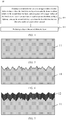
- FIGS. 5 to 9 are schematic structural diagrams of phased products in a process of producing a security chip according to an embodiment of the present application. A method for producing a security chip according to an embodiment of the present application will be described below with reference to FIGS. 5 to 9 .
- a first dielectric layer 11 as shown in FIG. 5 is selected, for example, a silicon wafer with a crystal orientation of 100 is selected as the first dielectric layer 11. Then, the first dielectric layer 11 is placed in a NaOH solution with a concentration of 8 wt%, and the NaOH solution is heated to at least 80°C to corrode the first dielectric layer 11 for at least 25 minutes. After corrosion, a structure as shown in FIG. 6 is formed on an upper surface of the first dielectric layer 11, that is, countless pyramid structures with different sizes are formed on the upper surface of the first dielectric layer 11.
- a second dielectric layer 12 as shown in FIG. 7 may be deposited on the upper surface of the first dielectric layer 11 by a CVD process.
- the second dielectric layer 12 may be a silicon dioxide layer.
- the second dielectric layer 12 may be polished by a chemical mechanical polishing (Chemical Mechanical Polishing, CMP) process, and an upper surface of the second dielectric layer 12 forms a flat plane as shown in FIG. 8 .
- CMP Chemical Mechanical Polishing
- a structure obtained in step 3 may be used as a handle wafer (handle wafer), and another substrate 131 may be used as a device wafer (device wafer), such as a silicon wafer. Then, a bonding (bonding) process may be used to permanently bond the substrate 131 and the second dielectric layer 12 together to form a structure as shown in FIG. 9 .
- the second dielectric layer 12 is located between the first dielectric layer 11 and the substrate 131, that is, the second dielectric layer is located between two wafers.
- a thickness of the device wafer may also be thinned to 10 microns by a CMP process.
- a device layer 132 may be produced first in the silicon layer with a thickness of 10 microns by a front-end-of-line (Front-End-Of-Line, FEOL) process, and then an interconnection layer 133 is produced by a back-end-of-line (Back-end-of-line, BEOL) process.
- Front-End-Of-Line FEOL
- BEOL back-end-of-line
- the FEOL process includes, but is not limited to, cleaning (clean), growth of a thermal oxidation (oxidation) layer, deposition (deposition), photolithography (photolithography), dry/wet etching (dry/wet etch), ion implantation (implantation), diffusion (diffusion), or the like, so that a transistor, a capacitor, and other devices are produced on a substrate or on a silicon layer of a silicon on insulator (Silicon On Insulator, SOI) wafer.
- SOI silicon On Insulator
- the produced wafer may be thinned from the back, for example, a thickness of the first dielectric layer 11 may be thinned, and then cut along a dicing path to obtain individual discrete chips.
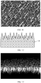
- FIGS. 10 and 11 are schematic diagrams of the first dielectric layer in the security chip as shown in FIG. 1 .
- a hot NaOH solution is used to perform anisotropic wet etching on a silicon wafer with a crystal orientation of 100, and a silicon wafer surface composed of a pyramid with a random size can be obtained.
- anisotropic wet etching on the silicon wafer with a crystal orientation of 100, a structure formed by a pyramidal protrusion or a pyramidal pit with a random size can be obtained, and an angle between an oblique surface of the pyramidal protrusion and a bottom surface of the first dielectric layer 11 is 54.7 degrees.
- FIGS. 10 and 11 are merely examples of the present application and should not be construed as limitation to the present application.
- a KOH solution, a TMAH solution, a Na 2 SiO 3 solution or a mixed corrosive agent of the above solutions may be used to obtain a similar topography.
- the upper surface of the first dielectric layer 11 may be provided with a rough surface (for example, the roughness is greater than 20 nm) or a porous surface by at least one of the following processes: a physical mechanical grinding process, a dry etching process, a metal assisted corrosion process, and an electrochemical corrosion process.
- a physical mechanical grinding process for example, a dry etching process, a metal assisted corrosion process, and an electrochemical corrosion process.
- the first dielectric layer 11 may be formed on the upper surface of the first dielectric layer 11, and the rough surface of the first dielectric layer 11 may be used for reflecting and/or scattering incident light, and preventing or slowing down a laser from penetrating the second dielectric layer 12, so that most of light cannot reach a logic or storage area on the front of the security chip, thereby achieving the purpose of resisting a laser attack.
- the dry etching (dry etching) process may include at least one of the following etching processes: reactive ion etching (reactive ion etching), plasma etching (plasma etching), ion beam etching (ion beam etching), or the like.
- reactive ion etching reactive ion etching
- plasma etching plasma etching
- ion beam etching ion beam etching
- an etching ratio may be changed by changing a mixing ratio of etching gas.
- each embodiment of the method 30 for producing the security chip listed above may be performed by robot or numerical control machining.
- the device software or process for performing the method 30 may perform the foregoing method 30 by executing a computer program code stored in a memory.
- the present application further provides a security chip produced according to the above production method.
- the present application further provides an electronic device including the security chip 10 described above, or an electronic device including the security chip produced according to the method 30 described above.
- sequence numbers of the foregoing processes do not mean execution sequences in various embodiments of the present application.
- the execution sequences of the processes should be determined according to functions and internal logic of the processes, and should not be construed as any limitation on the implementation processes of the embodiments of the present application.
- the disclosed integrated device, component in the integrated device, and method for producing the integrated device may be implemented in other manners.
- the integrated device embodiments described above are only exemplary.
- division of the layers is only a logical function division, and there may be other division methods in actual implementation.
Landscapes
- Engineering & Computer Science (AREA)
- Computer Security & Cryptography (AREA)
- Physics & Mathematics (AREA)
- General Physics & Mathematics (AREA)
- Computer Networks & Wireless Communication (AREA)
- Signal Processing (AREA)
- Theoretical Computer Science (AREA)
- Semiconductor Integrated Circuits (AREA)
- Health & Medical Sciences (AREA)
- Electromagnetism (AREA)
- Toxicology (AREA)
- Solid State Image Pick-Up Elements (AREA)
Abstract
Description
- Embodiments of the present application relate to the field of security chips, and more particularly, to a security chip, a security chip production method and an electronic device.
- A security chip is a special chip that can execute complex encryption and decryption algorithms.
- A secret key is stored in a special storage area of the security chip, and an attacker usually obtains the secret key by means of bypass attack, fault injection, and hardware Trojan horse.
- Laser fault injection is a very threatening attack method. Because there is a metal layer on the front of the security chip, it has a reflection effect on a laser. An attacker usually uses an infrared laser to illuminate a specific circuit on the front of the chip through the back of the security chip, and uses photocurrent generated by interaction between the laser and silicon to make the security chip output wrong results. Finally, the attacker can obtain the secret key by collecting errors with certain characteristics that occur at a specific time and at a specific location, and performing comparison and analysis with correct encryption results.
- In related technologies, a photosensitive module is usually provided in a security chip. When the photosensitive module detects a laser, an instruction command is issued to instruct erasure of a secret key stored in the security chip. However, the photosensitive module needs to occupy an additional chip area, which increases chip costs.
- Therefore, in a case that an additional chip area is not occupied, how to prevent a laser attack is an urgent technical problem to be solved in the art.
- Provided are a security chip, a security chip production method and an electronic device, which can ensure that a laser attack is prevented in a case that an additional chip area is not occupied.
- In a first aspect, provided is a security chip, including:
- a first dielectric layer;
- a second dielectric layer disposed on the first dielectric layer, where the first dielectric layer is an optically denser medium relative to the second dielectric layer, and a roughness of an upper surface of the first dielectric layer is greater than or equal to a preset threshold, so that light entering the second dielectric layer from the first dielectric layer is able to be totally reflected and/or scattered; and
- a semiconductor chip disposed on the second dielectric layer.
- Regarding vertical light incident in a vertical direction with respect to a lower surface of the first dielectric layer, when the roughness of the upper surface of the first dielectric layer is greater than or equal to the preset threshold, the vertical light can reach an interface between the first dielectric layer and the second dielectric layer, which increases its angle of incidence so that the angle of incidence is greater than a critical angle to meet conditions for total reflection; and the vertical light entering the first dielectric layer through total reflection can effectively reduce intensity of refracted light entering the second dielectric layer, so that most of the light cannot reach a logic or storage area on the front of the security chip, thereby achieving the purpose of resisting a laser attack.
- Regarding oblique light incident in an oblique direction with respect to the lower surface of the first dielectric layer, when the roughness of the upper surface of the first dielectric layer is greater than or equal to the preset threshold, light receiving area of the second dielectric layer for the oblique light can be reduced, which further reduces the amount of refracted light entering the second dielectric layer, thereby achieving the purpose of resisting a laser attack. In addition, compared with a propagation path of the vertical light in the first dielectric layer, a propagation path of the oblique light in the first dielectric layer is longer, which further increases the loss in the process that the oblique light reaches the first dielectric layer and the second dielectric layer, and further reduces intensity of the light entering the second dielectric layer.
- In addition, regardless of whether the interface between the first dielectric layer and the second dielectric layer is perpendicular or not perpendicular to incident light, the upper surface of the first dielectric layer whose roughness is greater than the preset threshold can scatter the light, so that a laser cannot be concentrated to a specific area, thereby further reducing intensity of refracted light entering the second dielectric layer.
- In summary, light incident from the lower surface of the first dielectric layer is able to be totally reflected or scattered by the upper surface of the first dielectric layer, thereby reducing intensity of light reaching the logic or storage area on the front of the security chip, thereby achieving the purpose of resisting a laser attack.
- In addition, by producing the semiconductor chip on a substrate formed by the first dielectric layer and the second dielectric layer, not only a laser attack can be ensured to be prevented in a case that an additional chip area is not occupied, but also a process flow is relatively simple and does not affect a processing method of the chip, which is convenient for mass production.
- In some possible embodiments, the preset threshold is 20 nm.
- In some possible embodiments, the upper surface of the first dielectric layer is provided with a spike-like structure or a hole-like structure.
- In some possible embodiments, the spike-like structure is formed by an irregularly-sized pyramidal protrusion or inverted pyramidal pit.
- In some possible embodiments, an oblique surface of the pyramidal protrusion and a bottom surface of the first dielectric layer form an angle of 54.7 degrees.
- In some possible embodiments, a material of the first dielectric layer is silicon (Si), and a material of the second dielectric layer is silicon dioxide (SiO2).
- An angled Si/SiO2 interface is formed inside the substrate. When light is transmitted from the back of the security chip to the front of the security chip in a vertical direction, the incident light is totally reflected at the Si/SiO2 interface, so that most of the laser cannot reach the logic or storage area on the front of the security chip, thereby achieving the purpose of resisting a laser attack.
- In some possible embodiments, the semiconductor chip includes:
- a substrate disposed on the second dielectric layer;
- a device layer disposed on an upper surface of the substrate; and
- an interconnection layer disposed on the device layer.
- In a second aspect, provided is an electronic device, including the security chip in the first aspect and any possible embodiment of the first aspect.
- In a third aspect, provided is a method for producing a security chip, including:
- forming a second dielectric layer on an upper surface of a first dielectric layer, where the first dielectric layer is an optically denser medium relative to the second dielectric layer, and a roughness of the upper surface of the first dielectric layer is greater than or equal to a preset threshold, so that light entering the second dielectric layer from the first dielectric layer is able to be totally reflected and/or scattered; and
- producing a semiconductor chip on the second dielectric layer.
- In some possible embodiments, the preset threshold is 20 nm.
- In some possible embodiments, before the forming the second dielectric layer on the upper surface of the first dielectric layer, the method further includes:
forming the upper surface of the first dielectric layer that is provided with a spike-like structure or a hole-like structure. - In some possible embodiments, the spike-like structure is formed by an irregularly-sized pyramidal protrusion or pyramidal pit.
- In some possible embodiments, an oblique surface of the pyramidal protrusion and a bottom surface of the first dielectric layer form an angle of 54.7 degrees.
- In some possible embodiments, the forming the upper surface of the first dielectric layer that is provided with the spike-like structure or the hole-like structure includes:
forming the upper surface of the first dielectric layer that is provided with the spike-like structure or the hole-like structure by at least one of the following processes:
a physical mechanical grinding process, a dry etching process, a metal assisted corrosion process, and an electrochemical corrosion process. - In some possible embodiments, the forming the upper surface of the first dielectric layer that is provided with the spike-like structure or the hole-like structure includes:
- placing the first dielectric layer in a corrosive agent; and
- heating the corrosive agent to form the upper surface of the first dielectric layer that is provided with the spike-like structure or the hole-like structure.
- In some possible embodiments, the corrosive agent includes at least one of the following:
a sodium hydroxide (NaOH) solution, a potassium hydroxide (KOH) solution, a tetramethylammonium hydroxide (TMAH) solution, and a sodium silicate (Na2SiO3) solution. - In some possible embodiments, the heating the corrosive agent includes:
heating the corrosive agent to a temperature above 80°C and performing corrosion for more than 25 minutes. - In some possible embodiments, a concentration of the corrosive agent is greater than or equal to 8 wt%.
- In some possible embodiments, the forming the second dielectric layer on the upper surface of the first dielectric layer includes:
forming the second dielectric layer on the upper surface of the first dielectric layer by a deposition process. - In some possible embodiments, before the producing the semiconductor chip on the second dielectric layer, the method further includes:
forming a flat upper surface of the second dielectric layer by a planarization process. - In some possible embodiments, the producing the semiconductor chip on the second dielectric layer includes:
- bonding a substrate on the second dielectric layer;
- producing a device layer on the substrate; and
- producing an interconnection layer on the device layer.
- In some possible embodiments, before the producing the device layer on the substrate, the method further includes:
thinning the substrate. - In some possible embodiments, the thinning the substrate includes:
thinning the substrate to 10 um or less. - In a fourth aspect, provided is a security chip, including the security chip produced in the method in the third aspect and any possible embodiment of the third aspect.
-
-
FIG. 1 is a schematic structural diagram of a security chip according to an embodiment of the present application. -
FIG. 2 is a schematic principle diagram of light propagating in two media according to an embodiment of the present application. -
FIG. 3 is a schematic principle diagram of light transmitting in the security chip shown inFIG. 1 . -
FIG. 4 is a schematic flow chart of a method for producing a security chip according to an embodiment of the present application. -
FIGS. 5 to 9 are schematic structural diagrams of phased products in a process of producing a security chip according to an embodiment of the present application. -
FIGS. 10 to 13 are schematic diagrams of a first dielectric layer in a security chip according to an embodiment of the present application. - Technical solutions in embodiments of the present application will be described hereinafter with reference to accompanying drawings.
- The embodiments of the present application are suitable for manufacturing various chips, especially a special chip or a security chip that can execute complex encryption and decryption algorithms. For example, the security chip may be a biochip (such as a fingerprint sensor chip), a chip provided with a circuit (such as a processor), various types of chips in the Internet of Things field, and so on. For example, the security chip may include an element such as a transistor, a resistor, a capacitor, and an inductor, and a wiring device or component. For example, the security chip may be a miniature electronic device or component carrying an integrated circuit (integrated circuit). This is not specifically limited by the present application. In addition, the technical solutions in the embodiments of the present application may be applied to various electronic devices, for example, portable or mobile computing devices such as a smart phone, a notebook computer, a tablet computer and a game device, and other electronic devices such as an electronic database, an automobile and an automated teller machine (Automated Teller Machine, ATM), which is not limited in the embodiments of the present application.
- It should be noted that, for convenience of description, in the embodiments of the present application, like reference numerals represent like components, and detailed description of the like components is omitted in different embodiments for the sake of brevity. It should be understood that dimensions such as thicknesses, lengths and widths of various components in embodiments of the present application shown in the drawings, as well as dimensions such as the overall thickness, length and width of an integrated device are merely illustrative, and should not constitute any limitation to the present application.
- In addition, for convenience of understanding, in embodiments shown below, for structures shown in different embodiments, like structures are denoted by like reference numerals, and detailed description of the same structures is omitted for brevity.
-
FIG. 1 is a schematic structural diagram of a security chip according to an embodiment of the present application. - Referring to
FIG. 1 , asecurity chip 10 includes afirst dielectric layer 11, asecond dielectric layer 12 and asemiconductor chip 13. Thesecond dielectric layer 12 is disposed on thefirst dielectric layer 11, and the 110 is disposed on thesecond dielectric layer 12. Further, thesemiconductor chip 13 can be etched and wired on a semiconductor sheet to produce a semiconductor device that can realize a certain function. For example, thesemiconductor chip 13 may include asubstrate 131, adevice layer 132 disposed on thesubstrate 131, and aninterconnection layer 133 disposed on thedevice layer 132. Theinterconnection layer 132 may be realized by disposing ametal layer 134 in a dielectric layer, which is not limited in the present application. - The
first dielectric layer 11 may be an optically denser medium relative to the second dielectric layer 12 (that is, a refractive index of thefirst dielectric layer 11 is greater than a refractive index of the second dielectric layer 12). In other words, thesecond dielectric layer 12 may be an optically thinner medium relative to the first dielectric layer 11 (that is, the refractive index of thesecond dielectric layer 12 is smaller than the refractive index of the first dielectric layer 11). Further, a roughness of an upper surface of thefirst dielectric layer 11 is greater than or equal to a preset threshold, so that light entering thesecond dielectric layer 12 vertically from thefirst dielectric layer 11 is able to be totally reflected and/or scattered. For example, the preset threshold may be 20 nm. - In order to facilitate the understanding of the solution of the present application, a total reflection phenomenon is briefly introduced below.
- Total reflection, also known as total internal reflection, refers to a phenomenon that when light is transmitted from an optically denser medium (that is, a refractive index of light in this medium is great) to an interface of an optically thinner medium (that is, a refractive index of light in this medium is small), it is all reflected back into the original medium.
-
FIG. 2 is a schematic principle diagram of light propagating in two media according to an embodiment of the present application. - Referring to
FIG. 2 , light enters from an optically denser medium 18 with a higher refractive index n 1 into an optically thinner medium 19 with a lower refractive index n 2. When an angle of incidence θ 1 offirst light 181 is smaller than a critical angle θc , the light 181 is refracted toward the optically thinner medium 19 to generate refracted light 182, while reflected toward the optically denser medium 18 to generate reflected light 183; and when an angle of incidence θ 2 ofsecond light 191 is greater than or equal to the critical angle θc , light refracted toward the optically thinner medium 19 disappears, and thesecond light 191 is only reflected toward the optically denser medium 18 to form reflected light 192, that is, thesecond light 191 is totally reflected, which is also called total internal reflection. The critical angle θc can also be considered as an angle of incidence when an angle of refraction is 90 degrees. - The critical angle θc can be determined by the following formula:

- It should be noted that the optically denser medium 18 and the optically thinner medium 19 are relatively speaking. When two substances are compared, one with a smaller refractive index is an optically thinner medium, and one with a greater refractive index is an optically denser medium. For example, if a refractive index of air is about 1, a refractive index of water is about 1.33, and a refractive index of glass is about 1.5, water is an optically denser medium relative to air, and water is an optically thinner medium relative to glass. The present application does not limit the specific materials of the
first dielectric layer 11 and thesecond dielectric layer 12, as long as it is ensured that the refractive index of thefirst dielectric layer 11 is greater than the refractive index of thesecond dielectric layer 12. - Based on the above analysis, it can be seen that regarding vertical light incident in a vertical direction with respect to a lower surface of the
first dielectric layer 11, when the roughness of the upper surface of thefirst dielectric layer 11 is greater than or equal to the preset threshold, the vertical light can reach an interface between thefirst dielectric layer 11 and thesecond dielectric layer 12, which increases its angle of incidence so that the angle of incidence is greater than a critical angle to meet conditions for total reflection; and the vertical light entering thefirst dielectric layer 11 through total reflection can effectively reduce intensity of refracted light entering thesecond dielectric layer 12, so that most of the light cannot reach a logic or storage area on the front of the security chip, thereby achieving the purpose of resisting a laser attack. - Regarding oblique light incident in an oblique direction with respect to the lower surface of the
first dielectric layer 11, when the roughness of the upper surface of thefirst dielectric layer 11 is greater than or equal to the preset threshold, light receiving area of thesecond dielectric layer 12 for the oblique light can be reduced, which further reduces the amount of refracted light entering thesecond dielectric layer 12, thereby achieving the purpose of resisting a laser attack. In addition, compared with a propagation path of the vertical light in thefirst dielectric layer 11, a propagation path of the oblique light in thefirst dielectric layer 11 is longer, which further increases the loss in the process that the oblique light reaches thefirst dielectric layer 11 and thesecond dielectric layer 12, and further reduces intensity of the light entering thesecond dielectric layer 12 and ensures safety of thesemiconductor chip 13. - In addition, regardless of whether the interface between the
first dielectric layer 11 and thesecond dielectric layer 12 is perpendicular or not perpendicular to incident light, the upper surface of thefirst dielectric layer 11 whose roughness is greater than the preset threshold can scatter the light, so that a laser cannot be concentrated to a specific area, thereby further reducing intensity of refracted light entering thesecond dielectric layer 12. - In summary, light incident from the lower surface of the
first dielectric layer 11 is able to be totally reflected or scattered by the upper surface of thefirst dielectric layer 11, thereby reducing intensity of light reaching the logic or storage area on the front of the security chip, thereby achieving the purpose of resisting a laser attack. - In addition, by producing the semiconductor chip on a substrate formed by the
first dielectric layer 11 and thesecond dielectric layer 12, not only a laser attack can be ensured to be prevented in a case that an additional chip area is not occupied, but also a process flow is relatively simple and does not affect a processing method of the chip, which is convenient for mass production. - Of course, the roughness of the upper surface of the
first dielectric layer 11 may also be smaller than the preset threshold. In this case, for example, regarding oblique light incident in an oblique direction with respect to the lower surface of thefirst dielectric layer 11, it can be ensured that its angle of incidence is greater than the critical angle to meet conditions for total reflection; and the oblique light entering thefirst dielectric layer 11 through total reflection can effectively reduce intensity of refracted light entering thesecond dielectric layer 12, so that most of the light cannot reach the logic or storage area on the front of the security chip, thereby achieving the purpose of resisting a laser attack. - As an example, the interface between the
first dielectric layer 11 and thesecond dielectric layer 12 may be provided with a spike-like structure or a hole-like structure. The spike-like structure is beneficial to increasing an angle of incidence of incident light perpendicular to thefirst dielectric layer 11, thereby causing the incident light to be totally reflected, and the hole-like structure is beneficial to scattering incident light. For example, the spike-like structure may be a structure shown inFIG. 1 . That is, the spike-like structure may be formed by an irregularly-sized pyramidal protrusion or inverted pyramidal pit. Optionally, an oblique surface of the pyramidal protrusion and a bottom surface of the first dielectric layer form an angle of 54.7 degrees. Of course, the spike-like structure may also be formed by a regular pyramidal protrusion or inverted pyramidal pit, and the angle between the oblique surface of the pyramidal protrusion and thefirst dielectric layer 11 may also be other numerical value, such as 60 degrees, which is not specifically limited in the present application. The pyramidal protrusion may have a regular or irregular sawtooth structure in cross section. -
FIG. 3 is a schematic principle diagram of light transmitting in the security chip shown inFIG. 1 . - In the following, with reference to
FIG. 3 , a technical principle of the present application will be described with an example that a material of thefirst dielectric layer 11 is silicon (Si), and a material of thesecond dielectric layer 12 is silicon dioxide (SiO2). - Referring to
FIG. 3 , the material of thefirst dielectric layer 11 is Si, and the material of thesecond dielectric layer 12 is silicon dioxide (SiO2).In an infrared waveband, a refractive index of silicon is about 3.42, a refractive index of SiO2 is about 1.45, and a critical angle of total reflection is about 25 degrees. Therefore, when an angle of incidence of light is greater than 25 degrees, total reflection will occur. - By taking incident light 21 as an example, the
incident light 21 is transmitted from thefirst dielectric layer 11 to thesecond dielectric layer 12 in a vertical direction, and an angle of incidence (54.7 degrees) of theincident light 21 is greater than the critical angle of total reflection (25 degrees), and therefore, theincident light 21 is totally reflected at an Si/SiO2 interface, that is, only reflected light 22 is generated. Then, since an angle of incidence (15.9 degrees) of the reflectedlight 22 is smaller than the critical angle of total reflection, multiple reflections and refractions occur, that is, reflectedlight 24 and the refracted light 23 are generated. It can be seen that only a very small amount of light (that is, the light 23) can enter thesecond dielectric layer 12 from thefirst dielectric layer 11. Similarly, most of incident light 25 will be reflected back in the form of reflected light 26, which effectively reduces intensity of light entering thesecond dielectric layer 12 and achieves the purpose of resisting a laser attack. - In addition, when incident light is not perpendicular to the Si/SiO2 interface, on the one hand, a propagation path of the light in the
first dielectric layer 11 is extended, and on the other hand, the light is blocked through a pyramidal protrusion at the Si/SiO2 interface, which can reduce light-receiving area of the second dielectric layer, and further can reduce intensity of refracted light entering thesecond dielectric layer 12, that is, reducing intensity of light reaching a logic or storage area on the front of a security chip, thereby preventing a laser attack. - In summary, by forming the angled Si/SiO2 interface, no matter whether incident light is perpendicular or not perpendicular to the Si/SiO2 interface, when the light is transmitted from the back of the security chip to the front of the security chip, intensity of light reaching the logic or storage area on the front of the security chip can be reduced, thereby achieving the purpose of resisting a laser attack.
-
FIG. 4 is a schematic flow chart of a method for producing a security chip according to an embodiment of the present application. - Referring to
FIG. 4 , amethod 30 for producing a security chip may include: - S31, forming a second dielectric layer on an upper surface of a first dielectric layer, where the first dielectric layer is an optically denser medium relative to the second dielectric layer, and a roughness of the upper surface of the first dielectric layer is greater than or equal to a preset threshold, so that light entering the second dielectric layer from the first dielectric layer is able to be totally reflected and/or scattered; and
- S32, producing a semiconductor chip on the second dielectric layer.
- Before the S31, the upper surface of the first dielectric layer whose roughness is greater than or equal to the preset threshold may be formed, so that light is totally reflected and/or scattered when the light enters the second dielectric layer from the first dielectric layer. For example, the preset threshold is 20 nm. That is, the second dielectric layer is formed on the upper surface of the first dielectric layer whose roughness is greater than or equal to the preset threshold. For example, the upper surface of the first dielectric layer that is provided with a spike-like structure or a hole-like structure is formed first, and then the second dielectric layer is formed on the upper surface of the first dielectric layer. For example, the spike-like structure may be a structure formed by a pyramidal protrusion or a pyramidal pit. Optionally, an oblique surface of the pyramidal protrusion and a bottom surface of the first dielectric layer form an angle of 54.7 degrees.
- For example, the first dielectric layer may be placed in a corrosive agent first; and then the corrosive agent is heated to form the upper surface of the first dielectric layer that is provided with the spike-like structure or the porous structure. The corrosive agent includes but is not limited to: a sodium hydroxide (NaOH) solution, a potassium hydroxide (KOH) solution, a tetramethylammonium hydroxide (TMAH) solution, and a sodium silicate (Na2SiO3) solution. A concentration of the corrosive agent is greater than or equal to a preset threshold, such as 8 wt%. Specifically, the corrosive agent may be heated to 80°C or above, and corroded for 25 minutes or above.
- In the S31, the second dielectric layer may be formed on the upper surface of the first dielectric layer by a deposition process.
- The deposition process includes but is not limited to:
a physical vapor deposition (Physical Vapor Deposition, PVD) process and/or a chemical vapor deposition (Chemical Vapor Deposition, CVD) process, for example, thermal oxidation, plasma enhanced chemical vapor deposition (Plasma Enhanced Chemical Vapor Deposition, PECVD), low pressure chemical vapor deposition (Low Pressure Chemical Vapor Deposition, LPCVD), atomic layer deposition (Atomic layer deposition, ALD), spin coating or spraying. - Before the S32, a flat upper surface of the second dielectric layer may be first formed by a planarization process, and then the second dielectric layer is deposited on the upper surface of the second dielectric layer.
- In the S32, a substrate may be first bonded on the second dielectric layer; then a device layer is produced on the substrate; and finally, an interconnection layer is produced on the device layer. Further, before the device layer is produced on the substrate, the substrate may further be thinned. For example, the substrate is thinned to 10 um or less.
-
FIGS. 5 to 9 are schematic structural diagrams of phased products in a process of producing a security chip according to an embodiment of the present application. A method for producing a security chip according to an embodiment of the present application will be described below with reference toFIGS. 5 to 9 . - First, a
first dielectric layer 11 as shown inFIG. 5 is selected, for example, a silicon wafer with a crystal orientation of 100 is selected as thefirst dielectric layer 11. Then, thefirst dielectric layer 11 is placed in a NaOH solution with a concentration of 8 wt%, and the NaOH solution is heated to at least 80°C to corrode thefirst dielectric layer 11 for at least 25 minutes. After corrosion, a structure as shown inFIG. 6 is formed on an upper surface of thefirst dielectric layer 11, that is, countless pyramid structures with different sizes are formed on the upper surface of thefirst dielectric layer 11. - A
second dielectric layer 12 as shown inFIG. 7 may be deposited on the upper surface of thefirst dielectric layer 11 by a CVD process. For example, thesecond dielectric layer 12 may be a silicon dioxide layer. - The
second dielectric layer 12 may be polished by a chemical mechanical polishing (Chemical Mechanical Polishing, CMP) process, and an upper surface of thesecond dielectric layer 12 forms a flat plane as shown inFIG. 8 . - A structure obtained in
step 3 may be used as a handle wafer (handle wafer), and anothersubstrate 131 may be used as a device wafer (device wafer), such as a silicon wafer. Then, a bonding (bonding) process may be used to permanently bond thesubstrate 131 and thesecond dielectric layer 12 together to form a structure as shown inFIG. 9 . Thesecond dielectric layer 12 is located between thefirst dielectric layer 11 and thesubstrate 131, that is, the second dielectric layer is located between two wafers. - Further, a thickness of the device wafer may also be thinned to 10 microns by a CMP process.
- A
device layer 132 may be produced first in the silicon layer with a thickness of 10 microns by a front-end-of-line (Front-End-Of-Line, FEOL) process, and then aninterconnection layer 133 is produced by a back-end-of-line (Back-end-of-line, BEOL) process. The FEOL process includes, but is not limited to, cleaning (clean), growth of a thermal oxidation (oxidation) layer, deposition (deposition), photolithography (photolithography), dry/wet etching (dry/wet etch), ion implantation (implantation), diffusion (diffusion), or the like, so that a transistor, a capacitor, and other devices are produced on a substrate or on a silicon layer of a silicon on insulator (Silicon On Insulator, SOI) wafer. When the BEOL process is used to produce an inter-metal dielectric layer and a metal layer, devices manufactured by the FEOL process can be connected to form a semiconductor chip with a specific function. It should be understood that thedevice layer 132 and theinterconnection layer 133 may be produced by an existing production process, which is not specifically limited in the present application. - The produced wafer may be thinned from the back, for example, a thickness of the
first dielectric layer 11 may be thinned, and then cut along a dicing path to obtain individual discrete chips. -
FIGS. 10 and11 are schematic diagrams of the first dielectric layer in the security chip as shown inFIG. 1 . - Referring to
FIGS. 10 and11 , a hot NaOH solution is used to perform anisotropic wet etching on a silicon wafer with a crystal orientation of 100, and a silicon wafer surface composed of a pyramid with a random size can be obtained. In other words, by performing anisotropic wet etching on the silicon wafer with a crystal orientation of 100, a structure formed by a pyramidal protrusion or a pyramidal pit with a random size can be obtained, and an angle between an oblique surface of the pyramidal protrusion and a bottom surface of thefirst dielectric layer 11 is 54.7 degrees. - It should be understood that
FIGS. 10 and11 are merely examples of the present application and should not be construed as limitation to the present application. - For example, a KOH solution, a TMAH solution, a Na2SiO3 solution or a mixed corrosive agent of the above solutions may be used to obtain a similar topography.
- For example, the upper surface of the
first dielectric layer 11 may be provided with a rough surface (for example, the roughness is greater than 20 nm) or a porous surface by at least one of the following processes: a physical mechanical grinding process, a dry etching process, a metal assisted corrosion process, and an electrochemical corrosion process. For example, a spike-like structure, a protrusion structure or a hole-like structure as shown inFIGS. 12 and 13 may be formed on the upper surface of thefirst dielectric layer 11, and the rough surface of thefirst dielectric layer 11 may be used for reflecting and/or scattering incident light, and preventing or slowing down a laser from penetrating thesecond dielectric layer 12, so that most of light cannot reach a logic or storage area on the front of the security chip, thereby achieving the purpose of resisting a laser attack. - The dry etching (dry etching) process may include at least one of the following etching processes: reactive ion etching (reactive ion etching), plasma etching (plasma etching), ion beam etching (ion beam etching), or the like. Preferably, an etching ratio may be changed by changing a mixing ratio of etching gas.
- It should be understood that the method embodiment and the product embodiment may correspond to each other, and similar description may refer to the product embodiment. For brevity, details are not described herein.
- It should also be understood that, each embodiment of the
method 30 for producing the security chip listed above may be performed by robot or numerical control machining. The device software or process for performing themethod 30 may perform the foregoingmethod 30 by executing a computer program code stored in a memory. - The present application further provides a security chip produced according to the above production method.
- The present application further provides an electronic device including the
security chip 10 described above, or an electronic device including the security chip produced according to themethod 30 described above. - It should be noted that, under a premise of no conflict, various embodiments and/or technical features in the various embodiments described in the present application may be combined with each other arbitrarily, and technical solutions obtained after the combination should also fall within the protection scope of the present application.
- It should be understood that sequence numbers of the foregoing processes do not mean execution sequences in various embodiments of the present application. The execution sequences of the processes should be determined according to functions and internal logic of the processes, and should not be construed as any limitation on the implementation processes of the embodiments of the present application.
- A person of ordinary skill in the art may be aware that, various exemplary production methods described in conjunction with the embodiments disclosed herein may be implemented by electronic hardware or a combination of computer software and electronic hardware. Whether these functions are performed by hardware or software depends on specific applications and designed constraint conditions of the technical solutions. Persons skilled in the art may use different methods to implement the described functions for each particular application, but it should not be considered that the implementation goes beyond the scope of the present application.
- In several embodiments provided in the present application, it should be understood that the disclosed integrated device, component in the integrated device, and method for producing the integrated device may be implemented in other manners. For example, the integrated device embodiments described above are only exemplary. For example, division of the layers is only a logical function division, and there may be other division methods in actual implementation.
- Described above are the specific embodiments of the present application only, but the protection scope of the present application is not limited thereto, those skilled who are familiar with the art could readily think of variations or substitutions within the technical scope disclosed by the present application, and these variations or substitutions shall fall within the protection scope of the present application. Therefore, the protection scope of claims should prevail over the protection scope of the present application.
Claims (23)
- A security chip, comprising:a first dielectric layer;a second dielectric layer disposed on the first dielectric layer, wherein the first dielectric layer is an optically denser medium relative to the second dielectric layer, and a roughness of an upper surface of the first dielectric layer is greater than or equal to a preset threshold, so that light entering the second dielectric layer from the first dielectric layer is able to be totally reflected and/or scattered; anda semiconductor chip disposed on the second dielectric layer.
- The security chip according to claim 1, wherein the preset threshold is 20 nm.
- The security chip according to claim 1 or 2, wherein the upper surface of the first dielectric layer is provided with a spike-like structure or a hole-like structure.
- The security chip according to claim 3, wherein the spike-like structure is formed by an irregularly-sized pyramidal protrusion or inverted pyramidal pit.
- The security chip according to claim 4, wherein an oblique surface of the pyramidal protrusion and a bottom surface of the first dielectric layer form an angle of 54.7 degrees.
- The security chip according to any one of claims 1 to 5, wherein a material of the first dielectric layer is silicon (Si), and a material of the second dielectric layer is silicon dioxide (SiO2).
- The security chip according to any one of claims 1 to 6, wherein the semiconductor chip comprises:a substrate disposed on the second dielectric layer;a device layer disposed on an upper surface of the substrate; andan interconnection layer disposed on the device layer.
- An electronic device, comprising:
the security chip according to any one of claims 1 to 7. - A method for producing a security chip, comprising:forming a second dielectric layer on an upper surface of a first dielectric layer, wherein the first dielectric layer is an optically denser medium relative to the second dielectric layer, and a roughness of the upper surface of the first dielectric layer is greater than or equal to a preset threshold, so that light entering the second dielectric layer from the first dielectric layer is able to be totally reflected and/or scattered; andproducing a semiconductor chip on the second dielectric layer.
- The method according to claim 9, wherein the preset threshold is 20 nm.
- The method according to claim 9 or 10, wherein before the forming the second dielectric layer on the upper surface of the first dielectric layer, the method further comprises:
forming the upper surface of the first dielectric layer that is provided with a spike-like structure or a hole-like structure. - The method according to claim 11, wherein the spike-like structure is formed by an irregularly-sized pyramidal protrusion or inverted pyramidal pit.
- The method according to claim 12, wherein an oblique surface of the pyramidal protrusion and a bottom surface of the first dielectric layer form an angle of 54.7 degrees.
- The method according to any one of claims 11 to 13, wherein the forming the upper surface of the first dielectric layer that is provided with the spike-like structure or the hole-like structure comprises:
forming the upper surface of the first dielectric layer that is provided with the spike-like structure or the hole-like structure by at least one of the following processes:
a physical mechanical grinding process, a dry etching process, a metal assisted corrosion process, and an electrochemical corrosion process. - The method according to any one of claims 11 to 14, wherein the forming the upper surface of the first dielectric layer that is provided with the spike-like structure or the hole-like structure comprises:placing the first dielectric layer in a corrosive agent; andheating the corrosive agent to form the upper surface of the first dielectric layer that is provided with the spike-like structure or the hole-like structure.
- The method according to claim 15, wherein the corrosive agent comprises at least one of the following:
a sodium hydroxide (NaOH) solution, a potassium hydroxide (KOH) solution, a tetramethylammonium hydroxide (TMAH) solution, or a sodium silicate (Na2SiO3) solution. - The method according to claim 15, wherein the heating the corrosive agent comprises:
heating the corrosive agent to a temperature above 80°C and performing corrosion for more than 25 minutes. - The method according to any one of claims 9 to 17, wherein the forming the second dielectric layer on the upper surface of the first dielectric layer comprises:
forming the second dielectric layer on the upper surface of the first dielectric layer by a deposition process. - The method according to any one of claims 9 to 18, wherein before the producing the semiconductor chip on the second dielectric layer, the method further comprises:
forming a flat upper surface of the second dielectric layer by a planarization process. - The method according to any one of claims 9 to 19, wherein the producing the semiconductor chip on the second dielectric layer comprises:bonding a substrate on the second dielectric layer;producing a device layer on the substrate; andproducing an interconnection layer on the device layer.
- The method according to claim 20, wherein before the producing the device layer on the substrate, the method further comprises:
thinning the substrate. - The method according to claim 21, wherein the thinning the substrate comprises:
thinning the substrate to 10 um or less. - A security chip, comprising:
the security chip produced in the method according to any one of claims 9 to 22.
Applications Claiming Priority (1)
| Application Number | Priority Date | Filing Date | Title |
|---|---|---|---|
| PCT/CN2019/099855 WO2021022566A1 (en) | 2019-08-08 | 2019-08-08 | Security chip, preparation method for security chip, and electronic device |
Publications (3)
| Publication Number | Publication Date |
|---|---|
| EP3800662A1 true EP3800662A1 (en) | 2021-04-07 |
| EP3800662A4 EP3800662A4 (en) | 2021-05-19 |
| EP3800662B1 EP3800662B1 (en) | 2022-03-02 |
Family
ID=74499036
Family Applications (1)
| Application Number | Title | Priority Date | Filing Date |
|---|---|---|---|
| EP19920630.1A Not-in-force EP3800662B1 (en) | 2019-08-08 | 2019-08-08 | Security chip and preparation method for security chip |
Country Status (4)
| Country | Link |
|---|---|
| US (1) | US11462490B2 (en) |
| EP (1) | EP3800662B1 (en) |
| CN (1) | CN113228270A (en) |
| WO (1) | WO2021022566A1 (en) |
Families Citing this family (4)
| Publication number | Priority date | Publication date | Assignee | Title |
|---|---|---|---|---|
| US11610846B2 (en) | 2019-04-12 | 2023-03-21 | Adeia Semiconductor Bonding Technologies Inc. | Protective elements for bonded structures including an obstructive element |
| US20220320015A1 (en) * | 2021-04-06 | 2022-10-06 | Globalfoundries U.S. Inc. | Backside structure for optical attack mitigation |
| US12278255B2 (en) * | 2021-06-11 | 2025-04-15 | Raytheon Company | Thin film obscurant for microelectronics |
| WO2023288021A1 (en) | 2021-07-16 | 2023-01-19 | Invensas Bonding Technologies, Inc. | Optically obstructive protective element for bonded structures |
Family Cites Families (15)
| Publication number | Priority date | Publication date | Assignee | Title |
|---|---|---|---|---|
| US6060773A (en) * | 1997-05-15 | 2000-05-09 | Nippon Telegraph And Telephone Corporation | Semiconductor chip and method of manufacturing the same |
| FR2784768A1 (en) * | 1998-10-16 | 2000-04-21 | Schlumberger Ind Sa | Protecting integrated circuits on cards from the effects of electromagnetic radiation by using silica doped with Phosphorus or Boron or an irregular surface or metallic screening |
| KR20010061785A (en) * | 1999-12-29 | 2001-07-07 | 박종섭 | Method of fabricating semiconductor device for preventing interconnection line from being shorted to metal contact |
| JP2007194566A (en) * | 2006-01-23 | 2007-08-02 | Renesas Technology Corp | Semiconductor device, and its process for fabrication |
| CN101809498A (en) * | 2007-09-25 | 2010-08-18 | 夏普株式会社 | Screen |
| KR101473773B1 (en) * | 2008-11-25 | 2014-12-17 | 삼성전자주식회사 | Recording medium for electrophotophotography |
| US9291752B2 (en) | 2013-08-19 | 2016-03-22 | 3M Innovative Properties Company | Retroreflecting optical construction |
| WO2010121019A1 (en) * | 2009-04-15 | 2010-10-21 | 3M Innovative Properties Company | Retroreflecting optical construction |
| US8618652B2 (en) * | 2010-04-16 | 2013-12-31 | Intel Corporation | Forming functionalized carrier structures with coreless packages |
| CN103837915A (en) * | 2014-03-19 | 2014-06-04 | 张家港康得新光电材料有限公司 | Retro-reflective film |
| CN104376357A (en) * | 2014-08-27 | 2015-02-25 | 北京中电华大电子设计有限责任公司 | Light attack resisting method for intelligent card |
| JP2016062031A (en) * | 2014-09-19 | 2016-04-25 | 大日本印刷株式会社 | Reflective screen, video display system |
| JP2017062299A (en) * | 2015-09-24 | 2017-03-30 | セイコーエプソン株式会社 | Electro-optic device and electronic apparatus |
| CN106326053B (en) | 2016-08-25 | 2022-02-01 | 深圳先进技术研究院 | Chip safety testing method and system based on fault injection |
| WO2020150938A1 (en) * | 2019-01-23 | 2020-07-30 | 深圳市汇顶科技股份有限公司 | Photoelectric sensor and preparation method therefor |
-
2019
- 2019-08-08 WO PCT/CN2019/099855 patent/WO2021022566A1/en not_active Ceased
- 2019-08-08 EP EP19920630.1A patent/EP3800662B1/en not_active Not-in-force
- 2019-08-08 CN CN201980001602.XA patent/CN113228270A/en active Pending
-
2020
- 2020-09-19 US US17/026,213 patent/US11462490B2/en active Active
Also Published As
| Publication number | Publication date |
|---|---|
| CN113228270A (en) | 2021-08-06 |
| EP3800662B1 (en) | 2022-03-02 |
| US11462490B2 (en) | 2022-10-04 |
| US20210043587A1 (en) | 2021-02-11 |
| WO2021022566A1 (en) | 2021-02-11 |
| EP3800662A4 (en) | 2021-05-19 |
Similar Documents
| Publication | Publication Date | Title |
|---|---|---|
| US11462490B2 (en) | Security chip, security chip production method and electronic device | |
| Otto et al. | Extremely low surface recombination velocities in black silicon passivated by atomic layer deposition | |
| US4427839A (en) | Faceted low absorptance solar cell | |
| Trompoukis et al. | Passivation of photonic nanostructures for crystalline silicon solar cells | |
| KR20130112877A (en) | Method for producing a solar cell having a textured front face and corresponding solar cell | |
| US8405169B2 (en) | Handling layer for transparent substrate | |
| CN103765603A (en) | Production method using dry etching of glass substrate having concave-convex film, glass substrate having concave-convex film, solar cell, and production method for solar cell | |
| Campbell et al. | Light trapping and reflection control in solar cells using tilted crystallographic surface textures | |
| CN102692682B (en) | Grating coupler and manufacturing method thereof | |
| CN106328581B (en) | Wafer bonding method and wafer bonding structure | |
| CN112349737B (en) | Semiconductor device, forming method thereof and image sensor | |
| CN211929489U (en) | Security Chips and Electronics | |
| Shih et al. | Surface characteristics optimization during wafer-level backside silicon removal for SOI wafers in 3D integration | |
| JP2775543B2 (en) | Photoelectric conversion device | |
| WO2021196039A1 (en) | Security chip, method for manufacturing security chip, and electronic device | |
| CN112558219A (en) | Optical device and manufacturing method thereof | |
| CN104752192A (en) | Method for manufacturing inclined surface on surface of semiconductor substrate | |
| CN105990377A (en) | CMOS image sensor and formation method thereof | |
| CN101350373A (en) | Solar cell wafer with multiple etching structures and manufacturing method thereof | |
| CN106910753A (en) | light pipe structure of image sensing element and manufacturing method thereof | |
| US20230170223A1 (en) | Semiconductor device and manufacturing method thereof | |
| TW201210050A (en) | Light scattering articles using hemispherical particles | |
| CN103390539A (en) | Method for manufacturing thin silicon wafer | |
| CN112530798A (en) | Semiconductor structure and manufacturing and thinning method thereof | |
| CN100373587C (en) | Metal interconnect process and method for removing silicide layer |
Legal Events
| Date | Code | Title | Description |
|---|---|---|---|
| STAA | Information on the status of an ep patent application or granted ep patent |
Free format text: STATUS: UNKNOWN |
|
| STAA | Information on the status of an ep patent application or granted ep patent |
Free format text: STATUS: THE INTERNATIONAL PUBLICATION HAS BEEN MADE |
|
| PUAI | Public reference made under article 153(3) epc to a published international application that has entered the european phase |
Free format text: ORIGINAL CODE: 0009012 |
|
| STAA | Information on the status of an ep patent application or granted ep patent |
Free format text: STATUS: REQUEST FOR EXAMINATION WAS MADE |
|
| 17P | Request for examination filed |
Effective date: 20200929 |
|
| AK | Designated contracting states |
Kind code of ref document: A1 Designated state(s): AL AT BE BG CH CY CZ DE DK EE ES FI FR GB GR HR HU IE IS IT LI LT LU LV MC MK MT NL NO PL PT RO RS SE SI SK SM TR |
|
| AX | Request for extension of the european patent |
Extension state: BA ME |
|
| A4 | Supplementary search report drawn up and despatched |
Effective date: 20210421 |
|
| RIC1 | Information provided on ipc code assigned before grant |
Ipc: G06F 21/00 20130101AFI20210415BHEP Ipc: G02B 5/124 20060101ALI20210415BHEP Ipc: H01L 23/00 20060101ALI20210415BHEP Ipc: H04L 9/00 20060101ALI20210415BHEP Ipc: G09C 1/00 20060101ALI20210415BHEP Ipc: G06Q 20/32 20120101ALI20210415BHEP Ipc: G07F 7/08 20060101ALI20210415BHEP Ipc: H01L 23/552 20060101ALN20210415BHEP |
|
| RIC1 | Information provided on ipc code assigned before grant |
Ipc: H01L 23/552 20060101ALN20210805BHEP Ipc: G07F 7/08 20060101ALI20210805BHEP Ipc: G06Q 20/32 20120101ALI20210805BHEP Ipc: G09C 1/00 20060101ALI20210805BHEP Ipc: H04L 9/00 20060101ALI20210805BHEP Ipc: H01L 23/00 20060101ALI20210805BHEP Ipc: G02B 5/124 20060101ALI20210805BHEP Ipc: G06F 21/00 20130101AFI20210805BHEP |
|
| REG | Reference to a national code |
Ref country code: DE Ref legal event code: R079 Ref document number: 602019012231 Country of ref document: DE Free format text: PREVIOUS MAIN CLASS: H01L0023552000 Ipc: G06F0021000000 |
|
| GRAP | Despatch of communication of intention to grant a patent |
Free format text: ORIGINAL CODE: EPIDOSNIGR1 |
|
| STAA | Information on the status of an ep patent application or granted ep patent |
Free format text: STATUS: GRANT OF PATENT IS INTENDED |
|
| RIC1 | Information provided on ipc code assigned before grant |
Ipc: H01L 23/552 20060101ALN20210929BHEP Ipc: G07F 7/08 20060101ALI20210929BHEP Ipc: G06Q 20/32 20120101ALI20210929BHEP Ipc: G09C 1/00 20060101ALI20210929BHEP Ipc: H04L 9/00 20060101ALI20210929BHEP Ipc: H01L 23/00 20060101ALI20210929BHEP Ipc: G02B 5/124 20060101ALI20210929BHEP Ipc: G06F 21/00 20130101AFI20210929BHEP |
|
| RIC1 | Information provided on ipc code assigned before grant |
Ipc: H01L 23/552 20060101ALN20211004BHEP Ipc: G07F 7/08 20060101ALI20211004BHEP Ipc: G06Q 20/32 20120101ALI20211004BHEP Ipc: G09C 1/00 20060101ALI20211004BHEP Ipc: H04L 9/00 20060101ALI20211004BHEP Ipc: H01L 23/00 20060101ALI20211004BHEP Ipc: G02B 5/124 20060101ALI20211004BHEP Ipc: G06F 21/00 20130101AFI20211004BHEP |
|
| DAV | Request for validation of the european patent (deleted) | ||
| DAX | Request for extension of the european patent (deleted) | ||
| INTG | Intention to grant announced |
Effective date: 20211021 |
|
| GRAS | Grant fee paid |
Free format text: ORIGINAL CODE: EPIDOSNIGR3 |
|
| GRAA | (expected) grant |
Free format text: ORIGINAL CODE: 0009210 |
|
| STAA | Information on the status of an ep patent application or granted ep patent |
Free format text: STATUS: THE PATENT HAS BEEN GRANTED |
|
| AK | Designated contracting states |
Kind code of ref document: B1 Designated state(s): AL AT BE BG CH CY CZ DE DK EE ES FI FR GB GR HR HU IE IS IT LI LT LU LV MC MK MT NL NO PL PT RO RS SE SI SK SM TR |
|
| REG | Reference to a national code |
Ref country code: GB Ref legal event code: FG4D |
|
| REG | Reference to a national code |
Ref country code: CH Ref legal event code: EP Ref country code: AT Ref legal event code: REF Ref document number: 1472846 Country of ref document: AT Kind code of ref document: T Effective date: 20220315 |
|
| REG | Reference to a national code |
Ref country code: DE Ref legal event code: R096 Ref document number: 602019012231 Country of ref document: DE |
|
| REG | Reference to a national code |
Ref country code: IE Ref legal event code: FG4D |
|
| REG | Reference to a national code |
Ref country code: LT Ref legal event code: MG9D |
|
| REG | Reference to a national code |
Ref country code: NL Ref legal event code: MP Effective date: 20220302 |
|
| PG25 | Lapsed in a contracting state [announced via postgrant information from national office to epo] |
Ref country code: SE Free format text: LAPSE BECAUSE OF FAILURE TO SUBMIT A TRANSLATION OF THE DESCRIPTION OR TO PAY THE FEE WITHIN THE PRESCRIBED TIME-LIMIT Effective date: 20220302 Ref country code: RS Free format text: LAPSE BECAUSE OF FAILURE TO SUBMIT A TRANSLATION OF THE DESCRIPTION OR TO PAY THE FEE WITHIN THE PRESCRIBED TIME-LIMIT Effective date: 20220302 Ref country code: NO Free format text: LAPSE BECAUSE OF FAILURE TO SUBMIT A TRANSLATION OF THE DESCRIPTION OR TO PAY THE FEE WITHIN THE PRESCRIBED TIME-LIMIT Effective date: 20220602 Ref country code: LT Free format text: LAPSE BECAUSE OF FAILURE TO SUBMIT A TRANSLATION OF THE DESCRIPTION OR TO PAY THE FEE WITHIN THE PRESCRIBED TIME-LIMIT Effective date: 20220302 Ref country code: HR Free format text: LAPSE BECAUSE OF FAILURE TO SUBMIT A TRANSLATION OF THE DESCRIPTION OR TO PAY THE FEE WITHIN THE PRESCRIBED TIME-LIMIT Effective date: 20220302 Ref country code: ES Free format text: LAPSE BECAUSE OF FAILURE TO SUBMIT A TRANSLATION OF THE DESCRIPTION OR TO PAY THE FEE WITHIN THE PRESCRIBED TIME-LIMIT Effective date: 20220302 Ref country code: BG Free format text: LAPSE BECAUSE OF FAILURE TO SUBMIT A TRANSLATION OF THE DESCRIPTION OR TO PAY THE FEE WITHIN THE PRESCRIBED TIME-LIMIT Effective date: 20220602 |
|
| REG | Reference to a national code |
Ref country code: AT Ref legal event code: MK05 Ref document number: 1472846 Country of ref document: AT Kind code of ref document: T Effective date: 20220302 |
|
| PG25 | Lapsed in a contracting state [announced via postgrant information from national office to epo] |
Ref country code: PL Free format text: LAPSE BECAUSE OF FAILURE TO SUBMIT A TRANSLATION OF THE DESCRIPTION OR TO PAY THE FEE WITHIN THE PRESCRIBED TIME-LIMIT Effective date: 20220302 Ref country code: LV Free format text: LAPSE BECAUSE OF FAILURE TO SUBMIT A TRANSLATION OF THE DESCRIPTION OR TO PAY THE FEE WITHIN THE PRESCRIBED TIME-LIMIT Effective date: 20220302 Ref country code: GR Free format text: LAPSE BECAUSE OF FAILURE TO SUBMIT A TRANSLATION OF THE DESCRIPTION OR TO PAY THE FEE WITHIN THE PRESCRIBED TIME-LIMIT Effective date: 20220603 Ref country code: FI Free format text: LAPSE BECAUSE OF FAILURE TO SUBMIT A TRANSLATION OF THE DESCRIPTION OR TO PAY THE FEE WITHIN THE PRESCRIBED TIME-LIMIT Effective date: 20220302 |
|
| PG25 | Lapsed in a contracting state [announced via postgrant information from national office to epo] |
Ref country code: NL Free format text: LAPSE BECAUSE OF FAILURE TO SUBMIT A TRANSLATION OF THE DESCRIPTION OR TO PAY THE FEE WITHIN THE PRESCRIBED TIME-LIMIT Effective date: 20220302 |
|
| PG25 | Lapsed in a contracting state [announced via postgrant information from national office to epo] |
Ref country code: SM Free format text: LAPSE BECAUSE OF FAILURE TO SUBMIT A TRANSLATION OF THE DESCRIPTION OR TO PAY THE FEE WITHIN THE PRESCRIBED TIME-LIMIT Effective date: 20220302 Ref country code: SK Free format text: LAPSE BECAUSE OF FAILURE TO SUBMIT A TRANSLATION OF THE DESCRIPTION OR TO PAY THE FEE WITHIN THE PRESCRIBED TIME-LIMIT Effective date: 20220302 Ref country code: RO Free format text: LAPSE BECAUSE OF FAILURE TO SUBMIT A TRANSLATION OF THE DESCRIPTION OR TO PAY THE FEE WITHIN THE PRESCRIBED TIME-LIMIT Effective date: 20220302 Ref country code: PT Free format text: LAPSE BECAUSE OF FAILURE TO SUBMIT A TRANSLATION OF THE DESCRIPTION OR TO PAY THE FEE WITHIN THE PRESCRIBED TIME-LIMIT Effective date: 20220704 Ref country code: EE Free format text: LAPSE BECAUSE OF FAILURE TO SUBMIT A TRANSLATION OF THE DESCRIPTION OR TO PAY THE FEE WITHIN THE PRESCRIBED TIME-LIMIT Effective date: 20220302 Ref country code: CZ Free format text: LAPSE BECAUSE OF FAILURE TO SUBMIT A TRANSLATION OF THE DESCRIPTION OR TO PAY THE FEE WITHIN THE PRESCRIBED TIME-LIMIT Effective date: 20220302 Ref country code: AT Free format text: LAPSE BECAUSE OF FAILURE TO SUBMIT A TRANSLATION OF THE DESCRIPTION OR TO PAY THE FEE WITHIN THE PRESCRIBED TIME-LIMIT Effective date: 20220302 |
|
| PG25 | Lapsed in a contracting state [announced via postgrant information from national office to epo] |
Ref country code: IS Free format text: LAPSE BECAUSE OF FAILURE TO SUBMIT A TRANSLATION OF THE DESCRIPTION OR TO PAY THE FEE WITHIN THE PRESCRIBED TIME-LIMIT Effective date: 20220702 Ref country code: AL Free format text: LAPSE BECAUSE OF FAILURE TO SUBMIT A TRANSLATION OF THE DESCRIPTION OR TO PAY THE FEE WITHIN THE PRESCRIBED TIME-LIMIT Effective date: 20220302 |
|
| REG | Reference to a national code |
Ref country code: DE Ref legal event code: R097 Ref document number: 602019012231 Country of ref document: DE |
|
| PLBE | No opposition filed within time limit |
Free format text: ORIGINAL CODE: 0009261 |
|
| STAA | Information on the status of an ep patent application or granted ep patent |
Free format text: STATUS: NO OPPOSITION FILED WITHIN TIME LIMIT |
|
| PG25 | Lapsed in a contracting state [announced via postgrant information from national office to epo] |
Ref country code: DK Free format text: LAPSE BECAUSE OF FAILURE TO SUBMIT A TRANSLATION OF THE DESCRIPTION OR TO PAY THE FEE WITHIN THE PRESCRIBED TIME-LIMIT Effective date: 20220302 |
|
| 26N | No opposition filed |
Effective date: 20221205 |
|
| PG25 | Lapsed in a contracting state [announced via postgrant information from national office to epo] |
Ref country code: SI Free format text: LAPSE BECAUSE OF FAILURE TO SUBMIT A TRANSLATION OF THE DESCRIPTION OR TO PAY THE FEE WITHIN THE PRESCRIBED TIME-LIMIT Effective date: 20220302 |
|
| PG25 | Lapsed in a contracting state [announced via postgrant information from national office to epo] |
Ref country code: MC Free format text: LAPSE BECAUSE OF FAILURE TO SUBMIT A TRANSLATION OF THE DESCRIPTION OR TO PAY THE FEE WITHIN THE PRESCRIBED TIME-LIMIT Effective date: 20220302 |
|
| REG | Reference to a national code |
Ref country code: CH Ref legal event code: PL |
|
| PG25 | Lapsed in a contracting state [announced via postgrant information from national office to epo] |
Ref country code: LU Free format text: LAPSE BECAUSE OF NON-PAYMENT OF DUE FEES Effective date: 20220808 Ref country code: LI Free format text: LAPSE BECAUSE OF NON-PAYMENT OF DUE FEES Effective date: 20220831 Ref country code: CH Free format text: LAPSE BECAUSE OF NON-PAYMENT OF DUE FEES Effective date: 20220831 |
|
| REG | Reference to a national code |
Ref country code: BE Ref legal event code: MM Effective date: 20220831 |
|
| PG25 | Lapsed in a contracting state [announced via postgrant information from national office to epo] |
Ref country code: IT Free format text: LAPSE BECAUSE OF FAILURE TO SUBMIT A TRANSLATION OF THE DESCRIPTION OR TO PAY THE FEE WITHIN THE PRESCRIBED TIME-LIMIT Effective date: 20220302 Ref country code: IE Free format text: LAPSE BECAUSE OF NON-PAYMENT OF DUE FEES Effective date: 20220808 Ref country code: FR Free format text: LAPSE BECAUSE OF NON-PAYMENT OF DUE FEES Effective date: 20220831 |
|
| PG25 | Lapsed in a contracting state [announced via postgrant information from national office to epo] |
Ref country code: BE Free format text: LAPSE BECAUSE OF NON-PAYMENT OF DUE FEES Effective date: 20220831 |
|
| PGFP | Annual fee paid to national office [announced via postgrant information from national office to epo] |
Ref country code: GB Payment date: 20230822 Year of fee payment: 5 |
|
| PGFP | Annual fee paid to national office [announced via postgrant information from national office to epo] |
Ref country code: DE Payment date: 20230821 Year of fee payment: 5 |
|
| PG25 | Lapsed in a contracting state [announced via postgrant information from national office to epo] |
Ref country code: CY Free format text: LAPSE BECAUSE OF FAILURE TO SUBMIT A TRANSLATION OF THE DESCRIPTION OR TO PAY THE FEE WITHIN THE PRESCRIBED TIME-LIMIT Effective date: 20220302 |
|
| PG25 | Lapsed in a contracting state [announced via postgrant information from national office to epo] |
Ref country code: MK Free format text: LAPSE BECAUSE OF FAILURE TO SUBMIT A TRANSLATION OF THE DESCRIPTION OR TO PAY THE FEE WITHIN THE PRESCRIBED TIME-LIMIT Effective date: 20220302 Ref country code: HU Free format text: LAPSE BECAUSE OF FAILURE TO SUBMIT A TRANSLATION OF THE DESCRIPTION OR TO PAY THE FEE WITHIN THE PRESCRIBED TIME-LIMIT; INVALID AB INITIO Effective date: 20190808 |
|
| PG25 | Lapsed in a contracting state [announced via postgrant information from national office to epo] |
Ref country code: TR Free format text: LAPSE BECAUSE OF FAILURE TO SUBMIT A TRANSLATION OF THE DESCRIPTION OR TO PAY THE FEE WITHIN THE PRESCRIBED TIME-LIMIT Effective date: 20220302 |
|
| PG25 | Lapsed in a contracting state [announced via postgrant information from national office to epo] |
Ref country code: MT Free format text: LAPSE BECAUSE OF FAILURE TO SUBMIT A TRANSLATION OF THE DESCRIPTION OR TO PAY THE FEE WITHIN THE PRESCRIBED TIME-LIMIT Effective date: 20220302 |
|
| REG | Reference to a national code |
Ref country code: DE Ref legal event code: R119 Ref document number: 602019012231 Country of ref document: DE |
|
| GBPC | Gb: european patent ceased through non-payment of renewal fee |
Effective date: 20240808 |
|
| PG25 | Lapsed in a contracting state [announced via postgrant information from national office to epo] |
Ref country code: DE Free format text: LAPSE BECAUSE OF NON-PAYMENT OF DUE FEES Effective date: 20250301 |
|
| PG25 | Lapsed in a contracting state [announced via postgrant information from national office to epo] |
Ref country code: GB Free format text: LAPSE BECAUSE OF NON-PAYMENT OF DUE FEES Effective date: 20240808 |