EP3799550B1 - Camera module and electronic device including the same - Google Patents
Camera module and electronic device including the same Download PDFInfo
- Publication number
- EP3799550B1 EP3799550B1 EP20184933.8A EP20184933A EP3799550B1 EP 3799550 B1 EP3799550 B1 EP 3799550B1 EP 20184933 A EP20184933 A EP 20184933A EP 3799550 B1 EP3799550 B1 EP 3799550B1
- Authority
- EP
- European Patent Office
- Prior art keywords
- camera module
- shielding structure
- electronic device
- protruding portion
- device housing
- Prior art date
- Legal status (The legal status is an assumption and is not a legal conclusion. Google has not performed a legal analysis and makes no representation as to the accuracy of the status listed.)
- Active
Links
Images















Classifications
-
- H—ELECTRICITY
- H04—ELECTRIC COMMUNICATION TECHNIQUE
- H04N—PICTORIAL COMMUNICATION, e.g. TELEVISION
- H04N23/00—Cameras or camera modules comprising electronic image sensors; Control thereof
- H04N23/57—Mechanical or electrical details of cameras or camera modules specially adapted for being embedded in other devices
-
- G—PHYSICS
- G03—PHOTOGRAPHY; CINEMATOGRAPHY; ANALOGOUS TECHNIQUES USING WAVES OTHER THAN OPTICAL WAVES; ELECTROGRAPHY; HOLOGRAPHY
- G03B—APPARATUS OR ARRANGEMENTS FOR TAKING PHOTOGRAPHS OR FOR PROJECTING OR VIEWING THEM; APPARATUS OR ARRANGEMENTS EMPLOYING ANALOGOUS TECHNIQUES USING WAVES OTHER THAN OPTICAL WAVES; ACCESSORIES THEREFOR
- G03B17/00—Details of cameras or camera bodies; Accessories therefor
- G03B17/02—Bodies
-
- G—PHYSICS
- G03—PHOTOGRAPHY; CINEMATOGRAPHY; ANALOGOUS TECHNIQUES USING WAVES OTHER THAN OPTICAL WAVES; ELECTROGRAPHY; HOLOGRAPHY
- G03B—APPARATUS OR ARRANGEMENTS FOR TAKING PHOTOGRAPHS OR FOR PROJECTING OR VIEWING THEM; APPARATUS OR ARRANGEMENTS EMPLOYING ANALOGOUS TECHNIQUES USING WAVES OTHER THAN OPTICAL WAVES; ACCESSORIES THEREFOR
- G03B30/00—Camera modules comprising integrated lens units and imaging units, specially adapted for being embedded in other devices, e.g. mobile phones or vehicles
-
- H—ELECTRICITY
- H04—ELECTRIC COMMUNICATION TECHNIQUE
- H04M—TELEPHONIC COMMUNICATION
- H04M1/00—Substation equipment, e.g. for use by subscribers
- H04M1/02—Constructional features of telephone sets
- H04M1/0202—Portable telephone sets, e.g. cordless phones, mobile phones or bar type handsets
- H04M1/026—Details of the structure or mounting of specific components
-
- H—ELECTRICITY
- H04—ELECTRIC COMMUNICATION TECHNIQUE
- H04M—TELEPHONIC COMMUNICATION
- H04M1/00—Substation equipment, e.g. for use by subscribers
- H04M1/02—Constructional features of telephone sets
- H04M1/0202—Portable telephone sets, e.g. cordless phones, mobile phones or bar type handsets
- H04M1/026—Details of the structure or mounting of specific components
- H04M1/0264—Details of the structure or mounting of specific components for a camera module assembly
-
- H—ELECTRICITY
- H04—ELECTRIC COMMUNICATION TECHNIQUE
- H04M—TELEPHONIC COMMUNICATION
- H04M1/00—Substation equipment, e.g. for use by subscribers
- H04M1/02—Constructional features of telephone sets
- H04M1/0202—Portable telephone sets, e.g. cordless phones, mobile phones or bar type handsets
- H04M1/026—Details of the structure or mounting of specific components
- H04M1/0277—Details of the structure or mounting of specific components for a printed circuit board assembly
-
- H—ELECTRICITY
- H04—ELECTRIC COMMUNICATION TECHNIQUE
- H04N—PICTORIAL COMMUNICATION, e.g. TELEVISION
- H04N23/00—Cameras or camera modules comprising electronic image sensors; Control thereof
- H04N23/45—Cameras or camera modules comprising electronic image sensors; Control thereof for generating image signals from two or more image sensors being of different type or operating in different modes, e.g. with a CMOS sensor for moving images in combination with a charge-coupled device [CCD] for still images
-
- H—ELECTRICITY
- H04—ELECTRIC COMMUNICATION TECHNIQUE
- H04N—PICTORIAL COMMUNICATION, e.g. TELEVISION
- H04N23/00—Cameras or camera modules comprising electronic image sensors; Control thereof
- H04N23/50—Constructional details
-
- H—ELECTRICITY
- H04—ELECTRIC COMMUNICATION TECHNIQUE
- H04N—PICTORIAL COMMUNICATION, e.g. TELEVISION
- H04N23/00—Cameras or camera modules comprising electronic image sensors; Control thereof
- H04N23/50—Constructional details
- H04N23/51—Housings
-
- H—ELECTRICITY
- H04—ELECTRIC COMMUNICATION TECHNIQUE
- H04N—PICTORIAL COMMUNICATION, e.g. TELEVISION
- H04N23/00—Cameras or camera modules comprising electronic image sensors; Control thereof
- H04N23/50—Constructional details
- H04N23/52—Elements optimising image sensor operation, e.g. for electromagnetic interference [EMI] protection or temperature control by heat transfer or cooling elements
-
- H—ELECTRICITY
- H04—ELECTRIC COMMUNICATION TECHNIQUE
- H04N—PICTORIAL COMMUNICATION, e.g. TELEVISION
- H04N23/00—Cameras or camera modules comprising electronic image sensors; Control thereof
- H04N23/50—Constructional details
- H04N23/54—Mounting of pick-up tubes, electronic image sensors, deviation or focusing coils
-
- H—ELECTRICITY
- H05—ELECTRIC TECHNIQUES NOT OTHERWISE PROVIDED FOR
- H05K—PRINTED CIRCUITS; CASINGS OR CONSTRUCTIONAL DETAILS OF ELECTRIC APPARATUS; MANUFACTURE OF ASSEMBLAGES OF ELECTRICAL COMPONENTS
- H05K9/00—Screening of apparatus or components against electric or magnetic fields
- H05K9/0007—Casings
- H05K9/005—Casings being nesting containers
-
- H—ELECTRICITY
- H05—ELECTRIC TECHNIQUES NOT OTHERWISE PROVIDED FOR
- H05K—PRINTED CIRCUITS; CASINGS OR CONSTRUCTIONAL DETAILS OF ELECTRIC APPARATUS; MANUFACTURE OF ASSEMBLAGES OF ELECTRICAL COMPONENTS
- H05K9/00—Screening of apparatus or components against electric or magnetic fields
- H05K9/0007—Casings
- H05K9/0058—Casings specially adapted for optoelectronic applications
-
- H—ELECTRICITY
- H05—ELECTRIC TECHNIQUES NOT OTHERWISE PROVIDED FOR
- H05K—PRINTED CIRCUITS; CASINGS OR CONSTRUCTIONAL DETAILS OF ELECTRIC APPARATUS; MANUFACTURE OF ASSEMBLAGES OF ELECTRICAL COMPONENTS
- H05K9/00—Screening of apparatus or components against electric or magnetic fields
- H05K9/0064—Earth or grounding circuit
Definitions
- the present disclosure relates to a camera module and an electronic device including the same, and more particularly, to a camera module including a shielding structure and an electronic device including the camera module.
- electromagnetic waves generated by the camera module may affect another electronic component in the electronic device and electromagnetic waves generated by another electronic component in the electronic device may affect the camera module. Therefore, in order to shield electromagnetic interference (EMI) and to improve electromagnetic compatibility (EMC), the camera module may have the shielding structure.
- EMI electromagnetic interference
- EMC electromagnetic compatibility
- US-A-2018/0261912 describes a vehicular antenna device capable of preventing reception trouble in a radio, a TV receiver, or the like due to noise by suppressing electromagnetic noise radiated from an electronic device or the like is provided.
- a vehicular antenna device is equipped with an antenna base which is fixed to a vehicle body via an attaching member, an antenna case which covers the antenna base, and an antenna element and a camera module as an electronic device which are disposed in an internal space surrounded by the antenna base and the antenna case.
- a camera module case surrounds a circuit board of the camera module and thereby shields it.
- the present invention provides an electronic device according to the appended claims. It is an aspect of the present disclosure to provide a camera module having high electromagnetic compatibility (EMC) and an electronic device including the same.
- the electronic device may include a main circuit board, wherein the camera module (CM-1) is connected to the main circuit board; an electronic component connected to the main circuit board; a device housing including a side wall, wherein the external structure is the device housing and the side wall surrounds a space in which the main circuit board, the electronic component, and the first camera module are positioned; and a front panel configured to cover the space in which the main circuit board, the electronic component, and the first camera module are positioned.
- the electronic device may include a main circuit board; wherein the first camera module connected to the main circuit board; a second camera module connected to the main circuit board; wherein the external structure is a flange that surrounds the first camera module and the second camera module; and a device housing configured to accommodate the main circuit board, the first camera module, the second camera module, and the flange.
- the electronic device includes a camera module comprising an image sensor; and a conductive shielding structure including an accommodating portion that surrounds the image sensor, and a protruding portion that protrudes from the accommodating portion and that contacts a conductive flange or a conductive portion of a device housing of the electronic device by elastic deformation.
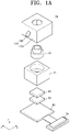
- FIG. 1A is an exploded perspective view of a camera module CM according to an embodiment.
- FIG. 1B is a cross-sectional view of a camera module CM according to an embodiment.
- the camera module CM may include a module circuit board 60, a connector 70, an image sensor 50, an optical filter 40, a lens assembly 20, a module housing 30, and a shielding structure 10.
- the module circuit board 60 may include, for example, a printed circuit board (PCB).
- the connector 70 may be connected to the module circuit board 60.
- the camera module CM may be connected to components that are outside of the camera module CM, for example, to a main circuit board 130 (refer to FIG. 4 ) through the connector 70.
- the image sensor 50 may be positioned on and connected to the module circuit board 60.
- the image sensor 50 may convert light into an electrical signal.
- the electrical signal generated by the image sensor 50 may be output to components outside of the camera module CM through the module circuit board 60 and the connector 70.
- the image sensor 50 may include, for example, a complementary metal oxide semiconductor (CMOS) sensor or a charge coupled device (CCD) sensor.
- CMOS complementary metal oxide semiconductor
- CCD charge coupled device
- the optical filter 40 may be positioned on the image sensor 50.
- the optical filter 40 may block or transmit a portion of a spectrum of light that enters the optical filter 40 and that has a particular wavelength.
- the optical filter 40 may include an infrared (IR) blocking filter that blocks near infrared (NIR) light (for example, light of wavelengths from about 700 nm to about 1,150 nm).
- IR infrared
- NIR near infrared
- the optical filter 40 may be omitted.
- the lens assembly 20 may be positioned on the optical filter 40.
- the lens assembly 20 may include at least one lens for focusing the light that passes therethrough.
- the module housing 30 may accommodate the image sensor 50, the optical filter 40, and the lens assembly 20. That is, the module housing 30 may surround the image sensor 50, the optical filter 40, and the lens assembly 20.
- the module housing 30 may fix the optical filter 40 and the lens assembly 20.
- the module housing 30 may be omitted and the shielding structure 10 may function as the module housing 30. That is, in some embodiments, the shielding structure 10 may accommodate and protect the image sensor 50, the optical filter 40, and the lens assembly 20.
- the shielding structure 10 may accommodate the module housing 30.
- the shielding structure 10 may surround the image sensor 50.
- the module housing 30 may include an opening or a window that exposes the lens assembly 20.
- the shielding structure 10 may shield components accommodated therein from electromagnetic interference (EMI).
- EMI electromagnetic interference
- the shielding structure 10 is conductive and may include a conductive material.
- the shielding structure 10 may include a metal such as copper (Cu), aluminum (Al), gold (Au), nickel (Ni), silver (Ag), iron (Fe), or a combination of the above metals.
- the shielding structure 10 may include an accommodating portion 10Q that accommodates, that is, that surrounds the image sensor 50, and a protruding portion 10P that protrudes outward from the accommodating portion 10Q.
- the accommodating portion 10Q may include side walls and a top.
- the accommodating portion 10Q may include four side walls and a top connected to each of the four side walls.
- the top of the accommodating portion 10Q may include the opening or the window through which light may enter the lens assembly 20.
- the protruding portion 10P of the shielding structure 10 may protrude from the side wall of the accommodating portion 10Q outward, for example, in a -X direction in FIG. 1A .
- the protruding portion 10P of the shielding structure 10 is conductive and may include a conductive material.
- the protruding portion 10P of the shielding structure 10 may include a material that is the same as the accommodating portion 10Q of the shielding structure 10. However, embodiments are not limited thereto and, in some embodiments, the protruding portion 10P of the shielding structure 10 may include a material that is different from the accommodating portion 10Q of the shielding structure 10.
- the protruding portion 10P of the shielding structure 10 may be integrated with the accommodating portion 10Q of the shielding structure 10. That is, there is not a real boundary between the protruding portion 10P and the accommodating portion 10Q of the shielding structure 10, and the protruding portion 10P of the shielding structure 10 may be distinguished from the accommodating portion 10Q of the shielding structure 10 by a virtual boundary.
- the protruding portion 10P and the accommodating portion 10Q of the shielding structure 10 may be formed as separate bodies, and then connected together, for example by bonding, adhesive, etc. That is, in some embodiments, there may be a real boundary between the protruding portion 10P and the accommodating portion 10Q of the shielding structure 10.
- the protruding portion 10P of the shielding structure 10 may contact an external structure (for example, a device housing 110 illustrated in FIG. 4 or a flange 170 illustrated in FIG. 14 ) that is positioned outside the camera module CM and of which at least a portion is conductive. Therefore, the shielding structure 10 may be electrically connected to the external structure and accordingly, electromagnetic compatibility (EMC) by the shielding structure may be improved by the shielding structure 10 illustrated in FIG. 1A . In addition, heat generated by the camera module CM may be transmitted to the external structure and accordingly, heat release performance by the shielding structure 10 may be improved. Therefore, the camera module CM according to an embodiment may have improved EMC and heat release performance.
- EMC electromagnetic compatibility
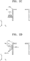
- FIGS. 2A to 2D are cross-sectional views illustrating examples of shielding structures 10a to 10d according to embodiments.
- protruding portions 10Pa to 10Pc of the shielding structures 10a to 10c may have various shapes.
- a protruding portion 10Pa of the shielding structure 10a illustrated in FIG. 2A may include a plurality of portions that extend in different directions.
- the protruding portion 10Pa may include a first portion 10Pa-1 that extends from the accommodating portion 10Q outward (for example, in the -X direction) and downward (for example, in a -Z direction), and a second portion 10Pa-2 that extends outward (for example, in the -X direction) and upward (for example, in a +Z direction).
- a protruding portion 10P of the shielding structure 10 illustrated in FIGS. 1A and 1B is straight, according to other embodiments, a protruding portion 10Pb of the shielding structure 10b may be curved as illustrated in FIG. 2B .
- a protruding portion 10Pc of the shielding structure 10c may have a more complicated shape like a coil shape.
- the protruding portions 10Pa to 10Pc of the shielding structures 10a to 10c may function as springs.
- the protruding portions 10Pa to 10Pc of the shielding structures 10a to 10c may be deformed and may have structures in which an elastic force may be applied to the outside by the deformation. Therefore, the protruding portions 10Pa to 10Pc of the shielding structures 10a to 10c may maintain contact with the external structure (for example, the device housing 110 illustrated in FIG. 4 or the flange 170 illustrated in FIG. 14 ) by elasticity.
- a shielding structure 10d may include an adhesive 10T and a protruding portion 10Pd.
- the adhesive 10T may attach the protruding portion 10Pd of the shielding structure 10d to the accommodating portion 10Q of the shielding structure 10d.
- the protruding portion 10Pd may include a first surface 10Pd-s that faces the accommodating portion 10Q and a second surface 10Pd-o that extends outward from the accommodating portion 10Q (as in FIG. 1A ), and the adhesive 10T may be between the accommodating portion 10Q and the first surface 10Pd-s of the protruding portion 10Pd that faces the accommodating portion 10Q, as illustrated in FIG. 2D .
- the adhesive 10T may be attached to a side wall of the accommodating portion 10Q, between the first surface 10Pd-s and the side wall of the accommodating portion 10Q.
- the adhesive 10T may include a conductive material.
- the adhesive 10T may be positioned on outside of the second surface 10Pd-o of the protruding portion 10Pd that faces outward, and may extend over the accommodating portion 10Q of the shielding structure 10d.
- the adhesive portion may not be provided between the protruding portion 10Pd and the side wall of the accommodating portion 10Q, but rather may be attached to the outside of the protruding portion 10Pd and may wrap around the side wall and at least a portion of the top of the accommodating portion 10Q.
- FIGS. 3A and 3B are cross-sectional views of camera modules CMa and CMb, respectively, according to embodiments.
- the camera module CMa may further include a prism 80 positioned in the module housing 30.
- the prism 80 may change a traveling direction of light. Light may enter the prism 80 through openings or windows of the module housing 30 and the shielding structure 10 in a vertical direction (for example, the -Z direction) and may exit of the prism 80 in a horizontal direction (for example, an X direction).
- the lens assembly 20 is positioned in the module housing 30 and may be oriented so that an optical axis of the lens assembly 20 runs parallel with the horizontal direction (for example, the X direction).
- the image sensor 50 may be erected so as to receive light that travels in the horizontal direction (for example, the X direction). That is, pixel arrays of the image sensor 50 may face the horizontal direction (for example, the -X direction).
- the camera module CMb may include a plurality of individual camera modules CM1 and CM2 and the plurality of individual camera modules CM1 and CM2 may share the shielding structure 10.
- the shielding structure 10 may include an opening or window corresponding to each of the plurality of individual camera modules CM1 and CM2, as illustrated in FIG. 3B .
- the camera module CMb may be referred to as a dual camera module.
- FIG. 4 is an exploded perspective view of an electronic device according to an embodiment.
- FIG. 5A is a plan view of the electronic device 100, from which a front panel is removed, according to an embodiment.
- FIG. 5B is a cross-sectional view of the electronic device 100, which is taken along the line B-B' of FIG. 5A .
- FIG. 5C is a cross-sectional view of the electronic device 100, which is taken along the line C-C' of FIG. 5A .
- the electronic device 100 may include an arbitrary portable electronic device such as a smart watch, smart glasses, a smart band, a tablet personal computer (PC), a personal digital assistant (PDA), a digital camera, or a game machine, an arbitrary home appliance such as a refrigerator, a washing machine, a drier, a vacuum cleaner, or a television set, an arbitrary transport unit such as a vehicle, a ship, or an airplane, an industrial electronic device, or a robot.
- a portable electronic device such as a smart watch, smart glasses, a smart band, a tablet personal computer (PC), a personal digital assistant (PDA), a digital camera, or a game machine
- PDA personal digital assistant
- a digital camera or a game machine
- an arbitrary home appliance such as a refrigerator, a washing machine, a drier, a vacuum cleaner, or a television set
- an arbitrary transport unit such as a vehicle, a ship, or an airplane, an industrial electronic device, or a robot.
- the electronic device 100 may include a main circuit board 130, a camera module (a front camera module CM-F and/or a rear camera module CM-R), an electronic component 140, a front panel 120, a rear panel 160, and a device housing 110.
- a camera module a front camera module CM-F and/or a rear camera module CM-R
- an electronic component 140 a front panel 120, a rear panel 160, and a device housing 110.
- the main circuit board 130 may include, for example, a PCB.
- the front camera module CM-F, the rear camera module CM-R, and the electronic component 140 may be connected to the main circuit board 130.
- Each of the front camera module CM-F and the rear camera module CM-R may be one of the camera modules CM, CMa, and CMb described with reference to FIGS. 1A to 3B .
- the front camera module CM-F may be oriented to face a front surface of the electronic device 100, that is, the front panel 120.
- the rear camera module CM-R may be oriented to face a rear surface of the electronic device 100, that is, the rear panel 160.
- the electronic component 140 may include, for example, memory, a processor, and/or an interface.
- the memory may include, for example, dynamic random access memory (DRAM), static random access memory (SRAM), flash memory, electrically erasable and programmable read-only memory (EEPROM), phase-change random access memory (PRAM), magnetic random access memory (MRAM), and/or resistive random access memory (RRAM).
- the processor may include, for example, a central processing unit (CPU), a graphics processing unit (GPU), and/or an application processor (AP).
- the interface may include, for example, a high definition multimedia interface (HDMI), a universal serial bus (USB), an interface, a secure digital (SD) card interface, and/or an audio interface.
- HDMI high definition multimedia interface
- USB universal serial bus
- SD secure digital
- the electronic device 100 may further include a battery 150 connected to the main circuit board 130.
- the electronic device 100 may further include a communication module, a microphone, a speaker, a fingerprint sensor, a gyro-sensor, a bio-sensor, an illuminance sensor, a humidity sensor, a temperature sensor, and/or a flash light.
- the front panel 120 and the rear panel 160 may face each other.
- the device housing 110 may be between the front panel 120 and the rear panel 160.
- the front panel 120, the device housing 110, and the rear panel 160 together may form an outer form of the electronic device 100. That is, the front panel 120, the device housing 110, and the rear panel 160 may be exposed to the outside of the electronic device 100.
- the front panel 120 may form a front surface of the electronic device 100
- the rear panel 160 may form a rear surface of the electronic device 100
- the device housing 110 may form a side surface of the electronic device 100.
- the main circuit board 130, the front camera module CM-F, the rear camera module CM-R, the electronic component 140, and the battery 150 may be accommodated in a space formed by the front panel 120, the device housing 110, and the rear panel 160.
- the device housing 110 may include a side wall that, for example, two-dimensionally surrounds the space in which the main circuit board 130, the front camera module CM-F, the rear camera module CM-R, the electronic component 140, and the battery 150 are positioned.
- the front panel 120 and the rear panel 160 may cover the space in which the main circuit board 130, the front camera module CM-F, the rear camera module CM-R, the electronic component 140, and the battery 150 are positioned.
- the front panel 120 may include a display 122.
- the front panel 120 may further include a front cover 121 including a transparent window on the display 122.
- the front panel 120 may further include a touch input panel (not shown) between the transparent window of the front cover 121 and the display 122.
- the front panel 120 may include an opening or a window 120A for the front camera module CM-F to receive light.
- the rear panel 160 may include an opening or a window 160A for the rear camera module CM-R to receive light.
- the device housing 110 may accommodate the main circuit board 130, the front camera module CM-F, the rear camera module CM-R, the electronic component 140, and the battery 150. At least a portion of the device housing 110 may be conductive and may include a conductive material.
- the device housing 110 may include a metal such as Cu, Al, Au, Ni, Ag, Fe, or a combination of the these metals.
- a protruding portion 10P-F of a shielding structure 10-F of the front camera module CM-F and a protruding portion 10P-R of a shielding structure 10-R of the rear camera module CM-R may contact the device housing 110.
- the protruding portion 10P-F of the shielding structure 10-F of the front camera module CM-F and the protruding portion 10P-R of the shielding structure 10-R of the rear camera module CM-R may protrude in two-dimensionally different directions.
- a direction, in which the protruding portion 10P-F of the shielding structure 10-F of the front camera module CM-F protrudes may be a +Y direction
- a direction, in which the protruding portion 10P-R of the shielding structure 10-R of the rear camera module CM-R protrudes may be the -X direction
- a surface of the front camera module CM-F, on which the protruding portion 10P-F of the shielding structure 10-F of the front camera module CM-F is positioned, and a surface of the rear camera module CM-R, on which the protruding portion 10P-R of the shielding structure 10-R of the rear camera module CM-R is positioned, may face different directions.
- the surface of the front camera module CM-F, on which the protruding portion 10P-F of the shielding structure 10-F of the front camera module CM-F is positioned may face the +Y direction
- the surface of the rear camera module CM-R, on which the protruding portion 10P-R of the shielding structure 10-R of the rear camera module CM-R is positioned may face the -X direction.
- FIG. 6 is a plan view of an electronic device 100, from which a front panel is removed, according to an embodiment.
- the protruding portion 10P-F of the shielding structure 10-F of the front camera module CM-F and the protruding portion 10P-R of the shielding structure 10-R of the rear camera module CM-R may protrude in the two-dimensionally same direction.
- a direction, in which the protruding portion 10P-F of the shielding structure 10-F of the front camera module CM-F protrudes, and a direction, in which the protruding portion 10P-R of the shielding structure 10-R of the rear camera module CM-R protrudes may be the +Y direction.
- the surface of the front camera module CM-F, on which the protruding portion 10P-F of the shielding structure 10-F of the front camera module CM-F is positioned, and the surface of the rear camera module CM-R, on which the protruding portion 10P-R of the shielding structure 10-R of the rear camera module CM-R is positioned, may face the same direction.
- the surface of the front camera module CM-F, on which the protruding portion 10P-F of the shielding structure 10-F of the front camera module CM-F is positioned, and the surface of the rear camera module CM-R, on which the protruding portion 10P-R of the shielding structure 10-R of the rear camera module CM-R is positioned, may face the +Y direction.
- FIG. 7 is a plan view of an electronic device from which a front panel is removed, according to an embodiment.
- the protruding portion 10P-F of the shielding structure 10-F of the front camera module CM-F contacts the device housing 110
- the protruding portion 10P-R of the shielding structure 10-R of the rear camera module CM-R may not contact the device housing 110 and may contact the shielding structure 10-F of the front camera module CM-F. Therefore, the shielding structure 10-R of the rear camera module CM-R may be electrically connected to the device housing 110 through the shielding structure 10_F of the front camera module CM-F.
- the front camera module CM-F is arranged not to two-dimensionally overlap a display 122 of the front panel 120.
- the rear camera module CM-R is arranged in a position remote from the side wall of the device housing 110. Since the rear camera module CM-R may contact the shielding structure 10-F of the front camera module CM-F, the flexibility of an arrangement design of the rear camera module CM-R may increase.
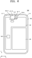
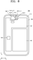
- FIG. 8 is a plan view of an electronic, from which a front panel is removed, device according to an embodiment.
- the shielding structure 10-F of the front camera module CM-F includes two protruding portions, for example, a first protruding portion 10P-F-1 and a second protruding portion 10P-F-2, whereas the shielding structure 10-R of the rear camera module CM-R may include no protruding portion.
- the first protruding portion 10P-F-1 of the shielding structure 10-F of the front camera module CM-F may contact the device housing 110 and the second protruding portion 10P-F-2 of the shielding structure 10-F of the front camera module CM-F may contact the shielding structure 10-R of the rear camera module CM-R. Therefore, the shielding structure 10-R of the rear camera module CM-R may be electrically connected to the device housing 110 through the shielding structure 10-F of the front camera module CM-F.
- the rear camera module CM-R including the shielding structure 10-R that includes no protruding portion may also be used, which is economical.
- the front camera module CM-F is to be arranged not to two-dimensionally overlap the display 122 of the front panel 120 but there are no such limitations on the arrangement of the rear camera module CM-R, although the rear camera module CM-R is arranged in a position remote from the side wall of the device housing 110, since the rear camera module CM-R may contact the shielding structure 10-F of the front camera module CM-F, the flexibility of an arrangement design of the rear camera module CM-R may increase.
- FIG. 9 is a cross-sectional view of a device housing according to an embodiment.
- the device housing 110 may include a conductive body 111 and an insulating coating 112 on the conductive body 111.
- the conductive body 111 may include any conductive material, for example, a metal such as Cu, Al, Au, Ni, Ag, Fe, or a combination of these metals.
- the insulating coating 112 may include, for example, a polymer.
- the protruding portions 10P-F and 10P-R of the shielding structures 10-F and 10-R of the camera modules CM-F and CM-R may contact the conductive body 111 of the device housing 110.
- the insulating coating 112 of the device housing 110 may expose at least a portion of the conductive body 111 of the device housing 110 and the protruding portions 10P-F and 10P-R of the shielding structures 10-F and 10-R of the camera modules CM-F and CM-R illustrated in FIGS. 5A to 5C may contact the exposed portion of the conductive body 111 of the device housing 110.
- the protruding portions 10P-F and 10P-R of the shielding structures 10-F and 10-R of the camera modules CM-F and CM-R illustrated in FIGS. 5A to 5C may pass through the insulating coating 112 of the device housing 110 and may contact the conductive body 111 of the device housing 110.
- FIG. 10 is an exploded perspective view of an electronic device 100b according to an embodiment.
- FIG. 11A is a plan view of the electronic device 100b, from which a front panel is removed, according to an embodiment.
- FIG. 11B is a cross-sectional view of the electronic device 100b, which is taken along the line B-B' of FIG. 11A .
- FIG. 11C is a cross-sectional view of the electronic device 100b, which is taken along the line C-C' of FIG. 11A .
- an electronic device 100b may omit the rear panel 160 illustrated in FIG. 4 and may include a device housing 110b that is different from the device housing 110 illustrated in FIG. 4 .
- the device housing 110b may further include a bottom 110B.
- the bottom 110B of the device housing 110b may face the front panel 120 and may be apart from the front panel 120.
- a side wall 110S of the device housing 110b may be between the front panel 120 and the bottom 110B of the device housing 110b.
- the device housing 110b may form at least a portion of an external form of the electronic device 100b.
- the bottom 110B of the device housing 110b may form a rear surface of the electronic device 100b and the side wall 110S of the device housing 110b may form a side surface of the electronic device 100b.
- the main circuit board 130, the front camera module CM-F, the rear camera module CM-R, the electronic component 140, and the battery 150 may be accommodated in a space formed by the front panel 120 and the device housing 110b.
- the side wall 110S of the device housing 110b may, for example, two-dimensionally surround the space in which the main circuit board 130, the front camera module CM-F, the rear camera module CM-R, the electronic component 140, and the battery 150 are positioned.
- the bottom 110B of the device housing 110b may cover the space in which the main circuit board 130, the front camera module CM-F, the rear camera module CM-R, the electronic component 140, and the battery 150 are positioned.
- the bottom 110B of the device housing 110b may include an opening or a window 110A through which the rear camera module CM-R receives light.
- the device housing 110b may further include an internal wall 110W positioned on the bottom 110B of the device housing 110b and in the space surrounded by the side wall 110S of the device housing 110b.
- the internal wall 110W of the device housing 110b may extend from the bottom 110B of the device housing 110b toward the front panel 120, for example, upward (in the +Z direction).
- the internal wall 110W of the device housing 110b may be positioned around the opening or window 110A of the bottom 110B of the device housing 110b.
- the internal wall 110W of the device housing 110b may be positioned around the rear camera module CM-R.
- the internal wall 110W of the device housing 110b may two-dimensionally and completely surround the rear camera module CM-R.
- the protruding portion 10P-F of the shielding structure 10-F of the front camera module CM-F may contact the side wall 110S of the device housing 110b, whereas the protruding portion 10P-R of the shielding structure 10-R of the rear camera module CM-R may contact the internal wall 110W of the device housing 110b.
- the front camera module CM-F is to be arranged not to two-dimensionally overlap the display 122, since the front camera module CM-F is close to the side wall 1105 of the device housing 110b, it is advantageous for the front camera module CM-F to contact the side wall 110S of the device housing 110b.
- the rear camera module CM-R is arranged in a position remote from the side wall 110S of the device housing 110b, since the rear camera module CM-R may contact the internal wall 110W of the device housing 110b, the flexibility of an arrangement design of the rear camera module CM-R may increase.
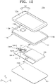
- FIG. 12 is an exploded perspective view of an electronic device 100c according to an embodiment.
- FIG. 13A is a plan view of the electronic device 100c, from which a rear panel is removed, according to an embodiment.
- FIG. 13B is a cross-sectional view of the electronic device 100c, which is taken along the line B-B' of FIG. 13A .
- FIG. 13C is a cross-sectional view of the electronic device 100c, which is taken along the line C-C' of FIG. 13A .
- an electronic device 100c may include a device housing 110c instead of the device housing 110b illustrated in FIG. 10 and may further include the rear panel 160 illustrated in FIG. 4 .
- the device housing 110c may have a structure in which the device housing 110b illustrated in FIG. 10 is reversed. That is, the bottom 110B of the device housing 110c may be positioned on the front panel 120, may face the rear panel 160, and may be apart from the rear panel 160.
- the side wall 110S of the device housing 110c may be between the rear panel 160 and the bottom 110B of the device housing 110c.
- the internal wall 110W of the device housing 110c may extend from the bottom 110B of the device housing 110c toward the rear panel 160, for example, downward (in the -Z direction).
- the internal wall 110W of the device housing 110c may not be positioned around the opening or window 110A of the bottom 110B of the device housing 110b but may be positioned around the rear camera module CM-R.
- the internal wall 110W of the device housing 110c may two-dimensionally and completely surround the rear camera module CM-R.
- FIG. 14 is an exploded perspective view of an electronic device 100d according to an embodiment.
- FIG. 15A is a plan view of the electronic device 100d, from which a front panel is removed, according to an embodiment.
- FIG. 15B is a cross-sectional view of the electronic device 100d, which is taken along the line B-B' of FIG. 15A .
- FIG. 15C is a cross-sectional view of the electronic device 100d, which is taken along the line C-C' of FIG. 15A .
- an electronic device 100d may further include a flange 170 accommodated in the device housing 110.
- the flange 170 may not be exposed to the outside of the electronic device 100d.
- the flange 170 may surround the rear camera module CM-R.
- the flange 170 may be conductive and may include a conductive material.
- the flange 170 may include a metal such as Cu, Al, Au, Ni, Ag, Fe, or a combination of these metals.
- the protruding portion 10P-F of the shielding structure 10-F of the front camera module CM-F may contact the device housing 110, whereas the protruding portion 10P-R of the shielding structure 10-R of the rear camera module CM-R may contact the flange 170.
- the front camera module CM-F is arranged not to two-dimensionally overlap the display 122, the front camera module CM-F is close to the side wall of the device housing 110 and it is advantageous for the front camera module CM-F to contact the side wall of the device housing 110.
- the rear camera module CM-R is arranged in a position remote from the side wall of the device housing 110, since the rear camera module CM-R may contact the flange 170, the flexibility of an arrangement design of the rear camera module CM-R may increase.
- FIG. 16 is a cross-sectional view of a flange 170 according to an embodiment.
- the flange 170 may include a conductive body 171 and an insulating coating 172 provided on the conductive body 171.
- the conductive body 171 may include a metal such as Cu, Al, Au, Ni, Ag, Fe, or a combination of these metals.
- the insulating coating 172 may include, for example, a polymer.
- the protruding portion 10P-R of the shielding structure10-R of the rear camera module CM-R illustrated in FIGS. 15A to 15C may contact the conductive body 171 of the flange 170. While FIGS. 15A-15C illustrate the flange 170 surrounding the rear camera module CM-R, embodiments are not limited thereto and, in some other embodiments, the flange 170 may be positioned alternatively to surround the front camera module CM-F, and the protruding portion 10P-F of the shielding structure 10-F of the camera module CM-F may alternatively contact the conductive body 171 of the flange 170.
- the insulating coating 172 of the flange 170 may expose at least a portion of the conductive body 171 of the flange 170 and the protruding portion 10P-R of the shielding structure 10-R of the rear camera module CM-R illustrated in FIGS. 15A to 15C may contact the exposed portion of the conductive body 171 of the flange 170.
- the protruding portion 10P-R of the shielding structure 10-R of the rear camera module CM-R illustrated in FIGS. 15A to 15C may pass through the insulating coating 172 of the flange 170 and contact the conductive body 171 of the flange 170.
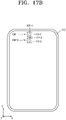
- FIGS. 17A to 17C are plan views illustrating a device housing and camera modules in electronic devices according to embodiments.
- a device housing 110 may include a first camera module CM-1 and a second camera module CM-2.
- a protruding portion 10P-1 of a shielding structure 10-1 of the first camera module CM-1 and a protruding portion 10P-2 of a shielding structure 10-2 of the second camera module CM-2 may contact the side wall of the device housing 110.
- both the first camera module CM-1 and the second camera module CM-2 may be front cameras, and in other embodiments both the first camera module CM-1 and the second camera module CM-2 may be rear cameras.
- a combination of the first camera module CM-1 and the second camera module CM-2 may be, for example, a combination of a wide-angle camera and a telephoto camera, a combination of a color camera and an infrared (IR) camera, or a combination of a main camera and a time-of-flight (TOF) camera.
- a combination of a wide-angle camera and a telephoto camera a combination of a color camera and an infrared (IR) camera
- IR infrared
- TOF time-of-flight
- the protruding portion 10P-1 of the shielding structure 10-1 of the first camera module CM-1 and the protruding portion 10P-2 of the shielding structure 10-2 of the second camera module CM-2 may protrude in the two-dimensionally same direction.
- a direction in which the protruding portion 10P-1 of the shielding structure 10-1 of the first camera module CM-1 protrudes and a direction in which the protruding portion 10P-2 of the shielding structure 10-2 of the second camera module CM-2 protrudes may be the +Y direction.
- a surface of the first camera module CM-1, on which the protruding portion 10P-1 of the shielding structure 10-1 of the first camera module CM-1 is positioned, and a surface of the second camera module CM-2, on which the protruding portion 10P-2 of the shielding structure 10-2 of the second camera module CM-2 is positioned, may face the same direction.
- the surface of the first camera module CM-1, on which the protruding portion 10P-1 of the shielding structure 10-1 of the first camera module CM-1 is positioned, and the surface of the second camera module CM-2, on which the protruding portion 10P-2 of the shielding structure 10-2 of the second camera module CM-2 is positioned may face the +Y direction.
- the protruding portion 10P-1 of the shielding structure 10-1 of the first camera module CM-1 and the protruding portion 10P-2 of the shielding structure 10-2 of the second camera module CM-2 may protrude in two-dimensionally different directions.
- the direction in which the protruding portion 10P-1 of the shielding structure 10-1 of the first camera module CM-1 protrudes may be the +Y direction
- the direction in which the protruding portion 10P-2 of the shielding structure 10-2 of the second camera module CM-2 protrudes may be the -X direction.
- the surface of the first camera module CM-1, on which the protruding portion 10P-1 of the shielding structure 10-1 of the first camera module CM-1 is positioned, and the surface of the second camera module CM-2, on which the protruding portion 10P-2 of the shielding structure 10-2 of the second camera module CM-2 is positioned, may face different directions.
- the surface of the first camera module CM-1, on which the protruding portion 10P-1 of the shielding structure 10-1 of the first camera module CM-1 is positioned may face the +Y direction
- the surface of the second camera module CM-2, on which the protruding portion 10P-2 of the shielding structure 10-2 of the second camera module CM-2 is positioned may face the -X direction.
- the protruding portion 10P-1 of the shielding structure 10-1 of the first camera module CM-1 may contact the side wall of the device housing 110, whereas the protruding portion 10P-2 of the shielding structure 10-2 of the second camera module CM-2 may contact the shielding structure 10-1 of the first camera module CM-1. Therefore, the shielding structure 10-2 of the second camera module CM-2 may be electrically connected to the device housing 110 through the shielding structure 10-1 of the first camera module CM-1. According to such embodiments, since the second camera module CM-2 may be arranged in a position remote from the side wall of the device housing 110, the flexibility of an arrangement design of the second camera module CM-2 may increase.
- the shielding structure 10-1 of the first camera module CM-1 includes a first protruding portion 10P-1-1 and a second protruding portion 10P-1-2, whereas the shielding structure 10-2 of the second camera module CM-2 may include no protruding portions.
- the first protruding portion 10P-1-1 of the shielding structure 10-1 of the first camera module CM-1 may contact the device housing 110, and the second protruding portion 10P-1-2 of the shielding structure 10-1 of the first camera module CM-1 may contact the shielding structure 10-2 of the second camera module CM-2.
- the shielding structure 10-2 of the second camera module CM-2 may be electrically connected to the device housing 110 through the shielding structure 10-1 of the first camera module CM-1.
- the second camera module CM-2 including the shielding structure 10-2 that includes no protruding portion may also be used, which is economical.
- the second camera module CM-2 since the second camera module CM-2 may be arranged in a position remote from the side wall of the device housing 110, the flexibility of an arrangement design of the second camera module CM-2 may increase.
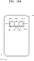
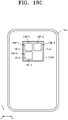
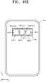
- FIGS. 18A to 18H are plan views illustrating a device housing and camera modules in electronic devices according to embodiments.
- a device housing 110b may include a first camera module CM-1, a second camera module CM-2, and a third camera module CM-3 accommodated therein.
- an internal wall 110W of the device housing 110b may be positioned around the first camera module CM-1, the second camera module CM-2, and the third camera module CM-3.
- the internal wall 110W of the device housing 110b may two-dimensionally and completely surround the first camera module CM-1, the second camera module CM-2, and the third camera module CM-3.
- the protruding portion 10P-1 of the shielding structure 10-1 of the first camera module CM-1, the protruding portion 10P-2 of the shielding structure 10-2 of the second camera module CM-2, and the protruding portion 10P-3 of the shielding structure 10-3 of the third camera module CM-3 may contact the internal wall 110W of the device housing 110b. It is noted that the protruding portions 10P-1, 10P-2, and 10P-3 all extend in the +Y direction in the example of FIG. 18A to contact the same side wall of the internal wall 110W, but embodiments are not limited thereto.
- one or more of the first camera module CM-1, the second camera module CM-2, and the third camera module CM-3 may have a protruding portion that contacts a different side wall of the internal wall 110W (see example of protruding portions contacting different side walls in FIG. 18B ).
- all of the first camera module CM-1, the second camera module CM-2, and the third camera module CM-3 may be front cameras. In other embodiments, all of the first camera module CM-1, the second camera module CM-2, and the third camera module CM-3 may be rear cameras.
- a combination of the first camera module CM-1, the second camera module CM-2, and the third camera module CM-3 may be, for example, a combination of a telephoto camera, a wide-angle camera, and an ultra-wide camera or a combination of the telephoto camera, the wide-angle camera, and a time-of-flight (TOF) camera.
- TOF time-of-flight
- the first camera module CM-1, the second camera module CM-2, and the third camera module CM-3 may be arranged in a row, as illustrated in FIG. 18A .
- the device housing 110b may have a long axis (a Y axis) and a short axis (an X axis) and the first camera module CM-1, the second camera module CM-2, and the third camera module CM-3 may be arranged in a direction of the short axis (the X axis) of the device housing 110b.
- the first camera module CM-1, the second camera module CM-2, and the third camera module CM-3 may be arranged in the direction of the long axis (the Y axis) of the device housing 110b.
- the first camera module CM-1, the second camera module CM-2, and the third camera module CM-3 may not be arranged in a row.
- the first camera module CM-1 and the second camera module CM-2 may be arranged in the short axis direction (the X axis direction) and the first camera module CM-1 and the third camera module CM-3 may be arranged in the long axis direction (the Y axis direction).
- the shielding structure 10-2 of the second camera module CM-2 may include a first protruding portion 10P-2-1 and a second protruding portion 10P-2-2 and the shielding structure 10-3 of the third camera module CM-3 may include one protruding portion 10P-3, whereas the shielding structure 10-1 of the first camera module CM-1 may include no protruding portion.
- the first protruding portion 10P-2-1 of the shielding structure 10-2 of the second camera module CM-2 may contact the internal wall 110W of the device housing 110b, and the second protruding portion 10P-2-2 of the shielding structure 10-2 of the second camera module CM-2 may contact the shielding structure 10-1 of the first camera module CM-1. Therefore, the shielding structure 10-1 of the first camera module CM-1 may be electrically connected to the internal wall 110W of the device housing 110b through the shielding structure 10-2 of the second camera module CM-2.
- the shielding structure 10-2 of the second camera module CM-2 may include a first protruding portion 10P-2-1, a second protruding portion 10P-2-2, and a third protruding portion 10P-2-3, whereas the shielding structure 10-1 of the first camera module CM-1 and the shielding structure 10-3 of the third camera module CM-3 each may include no protruding portions.
- the first protruding portion 10P-2-1 of the shielding structure 10-2 of the second camera module CM-2 may contact the internal wall 110W of the device housing 110b.
- the second protruding portion 10P-2-2 of the shielding structure 10-2 of the second camera module CM-2 may contact the shielding structure 10-1 of the first camera module CM-1.
- the third protruding portion 10P-2-3 of the shielding structure 10-2 of the second camera module CM-2 may contact the shielding structure 10-3 of the third camera module CM-3. Therefore, the shielding structure 10-1 of the first camera module CM-1 and the shielding structure 10-3 of the third camera module CM-3 may be electrically connected to the internal wall 110W of the device housing 110b through the shielding structure 10-2 of the second camera module CM-2.
- the protruding portion 10P-2 of the shielding structure 10-2 of the second camera module CM-2 may contact the internal wall 110W of the device housing 110b, whereas the protruding portion 10P-1 of the shielding structure 10-1 of the first camera module CM-1 and the protruding portion 10P-3 of the shielding structure 10-3 of the third camera module CM-3 may contact the shielding structure 10-2 of the second camera module CM-2. Therefore, the shielding structure 10-1 of the first camera module CM-1 and the shielding structure 10-3 of the third camera module CM-3 may be electrically connected to the internal wall 110W of the device housing 110b through the shielding structure 10-2 of the second camera module CM-2.
- an internal wall 110W-1 of the device housing 110b may further include a first portion between the first camera module CM-1 and the second camera module CM-2 and a second portion between the second camera module CM-2 and the third camera module CM-3.
- the internal wall 110W-1 of the device housing 110b may surround each of the first camera module CM-1, the second camera module CM-2, and the third camera module CM-3.
- the internal wall 110W-1 of the device housing 110b may be used for aligning the first to third camera modules CM-1, CM-2, and CM-3.
- an internal wall 110W-2 of the device housing 110b may be positioned only around the second camera module CM-2.
- the second camera module CM-2 may be positioned in a space surrounded by the internal wall 110W-2 of the device housing 110b, whereas the first camera module CM-1 and the third camera module CM-3 may be positioned outside the space surrounded by the internal wall 110W-2 of the device housing 110b.
- the protruding portion 10P-2 of the shielding structure 10-2 of the second camera module CM-2 may contact an internal surface of the internal wall 110W-2 of the device housing 110b, whereas the protruding portion 10P-1 of the shielding structure 10-1 of the first camera module CM-1 and the protruding portion 10P-3 of the shielding structure 10-3 of the third camera module CM-3 may contact an external surface of the internal wall 110W-2.
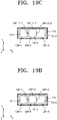
- FIGS. 19A to 19E are plan views illustrating a flange and camera modules in electronic devices according to embodiments.
- a flange 170 may include a first camera module CM-1, a second camera module CM-2, and a third camera module CM-3 accommodated therein.
- the flange 170 may surround the first camera module CM-1, the second camera module CM-2, and the third camera module CM-3.
- the protruding portion 10P-1 of the shielding structure 10-1 of the first camera module CM-1, the protruding portion 10P-2 of the shielding structure 10-2 of the second camera module CM-2, and the protruding portion 10P-3 of the shielding structure 10-3 of the third camera module CM-3 may contact the flange 170. It is noted that the protruding portions 10P-1, 10P-2, and 10P-3 all extend in the +Y direction in the example of FIG. 19A to contact the same side wall of the flange 170, but embodiments are not limited thereto.
- one or more of the first camera module CM-1, the second camera module CM-2, and the third camera module CM-3 may have a protruding portion that contacts a different side wall of the flange 170.
- the first camera module CM-1, the second camera module CM-2, and the third camera module CM-3 are illustrated in FIG. 19A as being arranged in a row in the X direction, similar to the description with reference to FIGS. 18A to 18C , the arrangement of the first camera module CM-1, the second camera module CM-2, and the third camera module CM-3 may be arranged in alternate arrangements such as those illustrated in FIGS. 18A-18C except with a flange 170.
- the shielding structure 10-2 of the second camera module CM-2 includes the first and second protruding portions 10P-2-1 and 10P-2-2 and the shielding structure 10-3 of the third camera module CM-3 includes the protruding portion 10P-3, whereas the shielding structure 10-1 of the first camera module CM-1 may include no protruding portion.
- the first protruding portion 10P-2-1 of the shielding structure 10-2 of the second camera module CM-2 may contact the flange 170 and the second protruding portion 10P-2-2 of the shielding structure 10-2 of the second camera module CM-2 may contact the shielding structure 10-1 of the first camera module CM-1. Therefore, the shielding structure 10-1 of the first camera module CM-1 may be electrically connected to the flange 170 through the shielding structure 10-2 of the second camera module CM-2.
- the shielding structure 10-2 of the second camera module CM-2 includes the first to third protruding portions 10P-2-1, 10P-2-2, and 10P-2-3, the shielding structure 10-1 of the first camera module CM-1 and the shielding structure 10-3 of the third camera module CM-3 each may include no protruding portions.
- the first protruding portion 10P-2-1 of the shielding structure 10-2 of the second camera module CM-2 may contact the flange 170.
- the second protruding portion 10P-2-2 of the shielding structure 10-2 of the second camera module CM-2 may contact the shielding structure 10-1 of the first camera module CM-1.
- the third protruding portion 10P-2-3 of the shielding structure 10-2 of the second camera module CM-2 may contact the shielding structure 10-3 of the third camera module CM-3. Therefore, the shielding structure 10-1 of the first camera module CM-1 and the shielding structure 10-3 of the third camera module CM-3 may be electrically connected to the flange 170 through the shielding structure 10-2 of the second camera module CM-2.
- the protruding portion 10P-2 of the shielding structure 10-2 of the second camera module CM-2 may contact the flange 170, whereas the protruding portion 10P-1 of the shielding structure 10-1 of the first camera module CM-1 and the protruding portion 10P-3 of the shielding structure 10-3 of the third camera module CM-3 may contact the shielding structure 10-2 of the second camera module CM-2. Therefore, the shielding structure 10-1 of the first camera module CM-1 and the shielding structure 10-3 of the third camera module CM-3 may be electrically connected to the flange 170 through the shielding structure 10-2 of the second camera module CM-2.
- the flange 170-1 may further include a first portion between the first camera module CM-1 and the second camera module CM-2 and a second portion between the second camera module CM-2 and the third camera module CM-3. That is, the flange 170 may surround each of the first camera module CM-1, the second camera module CM-2, and the third camera module CM-3. According to such embodiments, the flange 170-1 may be used for aligning the first to third camera modules CM-1, CM-2, and CM-3.
Landscapes
- Engineering & Computer Science (AREA)
- Signal Processing (AREA)
- Multimedia (AREA)
- Microelectronics & Electronic Packaging (AREA)
- Physics & Mathematics (AREA)
- General Physics & Mathematics (AREA)
- Human Computer Interaction (AREA)
- Electromagnetism (AREA)
- Studio Devices (AREA)
- Camera Bodies And Camera Details Or Accessories (AREA)
- Shielding Devices Or Components To Electric Or Magnetic Fields (AREA)
Description
- The present disclosure relates to a camera module and an electronic device including the same, and more particularly, to a camera module including a shielding structure and an electronic device including the camera module.
- In an electronic device including a camera module, electromagnetic waves generated by the camera module may affect another electronic component in the electronic device and electromagnetic waves generated by another electronic component in the electronic device may affect the camera module. Therefore, in order to shield electromagnetic interference (EMI) and to improve electromagnetic compatibility (EMC), the camera module may have the shielding structure.
-
US-A-2018/0261912 describes a vehicular antenna device capable of preventing reception trouble in a radio, a TV receiver, or the like due to noise by suppressing electromagnetic noise radiated from an electronic device or the like is provided. A vehicular antenna device is equipped with an antenna base which is fixed to a vehicle body via an attaching member, an antenna case which covers the antenna base, and an antenna element and a camera module as an electronic device which are disposed in an internal space surrounded by the antenna base and the antenna case. A camera module case surrounds a circuit board of the camera module and thereby shields it. - The present invention provides an electronic device according to the appended claims. It is an aspect of the present disclosure to provide a camera module having high electromagnetic compatibility (EMC) and an electronic device including the same. The electronic device may include a main circuit board, wherein the camera module (CM-1) is connected to the main circuit board; an electronic component connected to the main circuit board; a device housing including a side wall, wherein the external structure is the device housing and the side wall surrounds a space in which the main circuit board, the electronic component, and the first camera module are positioned; and a front panel configured to cover the space in which the main circuit board, the electronic component, and the first camera module are positioned.
- The electronic device may include a main circuit board; wherein the first camera module connected to the main circuit board; a second camera module connected to the main circuit board; wherein the external structure is a flange that surrounds the first camera module and the second camera module; and a device housing configured to accommodate the main circuit board, the first camera module, the second camera module, and the flange.
- The electronic device includes a camera module comprising an image sensor; and a conductive shielding structure including an accommodating portion that surrounds the image sensor, and a protruding portion that protrudes from the accommodating portion and that contacts a conductive flange or a conductive portion of a device housing of the electronic device by elastic deformation.
- Various embodiments will be more clearly understood from the following detailed description taken in conjunction with the accompanying drawings, in which:
-
FIG. 1A is an exploded perspective view of a camera module according to an embodiment; -
FIG. 1B is a cross-sectional view of a camera module according to an embodiment; -
FIGS. 2A to 2D are cross-sectional views of shielding structures according to embodiments; -
FIGS. 3A to 3B are cross-sectional views of camera modules according to embodiments; -
FIG. 4 is an exploded perspective view of an electronic device according to an embodiment; -
FIG. 5A is a plan view of an 100 from which a front panel is removed, according to an embodiment; -
FIG. 5B is a cross-sectional view of an electronic device, which is taken along the line B-B' ofFIG. 5A , according to an embodiment; -
FIG. 5C is a cross-sectional view of an electronic device, which is taken along the line C-C' ofFIG. 5A , according to an embodiment; -
FIGS. 6 to 8 are plan views of electronic devices, from which a front panel is removed, according to embodiments; -
FIG. 9 is a cross-sectional view of a device housing according to an embodiment; -
FIG. 10 is an exploded perspective view of an electronic device according to an embodiment; -
FIG. 11A is a plan view of an electronic device, from which a front panel is removed, according to an embodiment; -
FIG. 11B is a cross-sectional view of an electronic device, which is taken along the line B-B' ofFIG. 11A , according to an embodiment; -
FIG. 11C is a cross-sectional view of an electronic device, which is taken along the line C-C' ofFIG. 11A , according to an embodiment; -
FIG. 12 is an exploded perspective view of an electronic device according to an embodiment; -
FIG. 13A is a plan view of an electronic device, from which a rear panel is removed, according to an embodiment; -
FIG. 13B is a cross-sectional view of an electronic device, which is taken along the line B-B' ofFIG. 13A , according to an embodiment; -
FIG. 13C is a cross-sectional view of an electronic device, which is taken along the line C-C' ofFIG. 13A , according to an embodiment; -
FIG. 14 is an exploded perspective view of an electronic device according to an embodiment; -
FIG. 15A is a plan view of an electronic device, from which a front panel is removed, according to an embodiment; -
FIG. 15B is a cross-sectional view of an electronic device, which is taken along the line B-B' ofFIG. 15A , according to an embodiment; -
FIG. 15C is a cross-sectional view of an electronic device, which is taken along the line C-C' ofFIG. 15A , according to an embodiment; -
FIG. 16 is a cross-sectional view of a flange according to an embodiment; -
FIGS. 17A to 17C are plan views illustrating a device housing and camera modules in electronic devices according to embodiments; -
FIGS. 18A to 18H are plan views illustrating a device housing and camera modules in electronic devices according to embodiments; and -
FIGS. 19A to 19E are plan views illustrating a flange and camera modules in electronic devices according to embodiments. -
FIG. 1A is an exploded perspective view of a camera module CM according to an embodiment.FIG. 1B is a cross-sectional view of a camera module CM according to an embodiment. - Referring to
FIGS. 1A and1B , the camera module CM may include amodule circuit board 60, aconnector 70, animage sensor 50, anoptical filter 40, alens assembly 20, amodule housing 30, and a shieldingstructure 10. Themodule circuit board 60 may include, for example, a printed circuit board (PCB). Theconnector 70 may be connected to themodule circuit board 60. The camera module CM may be connected to components that are outside of the camera module CM, for example, to a main circuit board 130 (refer toFIG. 4 ) through theconnector 70. - The
image sensor 50 may be positioned on and connected to themodule circuit board 60. Theimage sensor 50 may convert light into an electrical signal. The electrical signal generated by theimage sensor 50 may be output to components outside of the camera module CM through themodule circuit board 60 and theconnector 70. Theimage sensor 50 may include, for example, a complementary metal oxide semiconductor (CMOS) sensor or a charge coupled device (CCD) sensor. - The
optical filter 40 may be positioned on theimage sensor 50. Theoptical filter 40 may block or transmit a portion of a spectrum of light that enters theoptical filter 40 and that has a particular wavelength. For example, theoptical filter 40 may include an infrared (IR) blocking filter that blocks near infrared (NIR) light (for example, light of wavelengths from about 700 nm to about 1,150 nm). In some embodiments, theoptical filter 40 may be omitted. - The
lens assembly 20 may be positioned on theoptical filter 40. Thelens assembly 20 may include at least one lens for focusing the light that passes therethrough. Themodule housing 30 may accommodate theimage sensor 50, theoptical filter 40, and thelens assembly 20. That is, themodule housing 30 may surround theimage sensor 50, theoptical filter 40, and thelens assembly 20. Themodule housing 30 may fix theoptical filter 40 and thelens assembly 20. In some embodiments, themodule housing 30 may be omitted and the shieldingstructure 10 may function as themodule housing 30. That is, in some embodiments, the shieldingstructure 10 may accommodate and protect theimage sensor 50, theoptical filter 40, and thelens assembly 20. - The shielding
structure 10 may accommodate themodule housing 30. The shieldingstructure 10 may surround theimage sensor 50. In order that light may enter thelens assembly 20, themodule housing 30 may include an opening or a window that exposes thelens assembly 20. The shieldingstructure 10 may shield components accommodated therein from electromagnetic interference (EMI). The shieldingstructure 10 is conductive and may include a conductive material. For example, the shieldingstructure 10 may include a metal such as copper (Cu), aluminum (Al), gold (Au), nickel (Ni), silver (Ag), iron (Fe), or a combination of the above metals. - The shielding
structure 10 may include anaccommodating portion 10Q that accommodates, that is, that surrounds theimage sensor 50, and a protrudingportion 10P that protrudes outward from theaccommodating portion 10Q. Theaccommodating portion 10Q may include side walls and a top. For example, theaccommodating portion 10Q may include four side walls and a top connected to each of the four side walls. The top of theaccommodating portion 10Q may include the opening or the window through which light may enter thelens assembly 20. The protrudingportion 10P of the shieldingstructure 10 may protrude from the side wall of theaccommodating portion 10Q outward, for example, in a -X direction inFIG. 1A . The protrudingportion 10P of the shieldingstructure 10 is conductive and may include a conductive material. The protrudingportion 10P of the shieldingstructure 10 may include a material that is the same as theaccommodating portion 10Q of the shieldingstructure 10. However, embodiments are not limited thereto and, in some embodiments, the protrudingportion 10P of the shieldingstructure 10 may include a material that is different from theaccommodating portion 10Q of the shieldingstructure 10. - In some embodiments, the protruding
portion 10P of the shieldingstructure 10 may be integrated with theaccommodating portion 10Q of the shieldingstructure 10. That is, there is not a real boundary between the protrudingportion 10P and theaccommodating portion 10Q of the shieldingstructure 10, and the protrudingportion 10P of the shieldingstructure 10 may be distinguished from theaccommodating portion 10Q of the shieldingstructure 10 by a virtual boundary. In other embodiments, the protrudingportion 10P and theaccommodating portion 10Q of the shieldingstructure 10 may be formed as separate bodies, and then connected together, for example by bonding, adhesive, etc. That is, in some embodiments, there may be a real boundary between the protrudingportion 10P and theaccommodating portion 10Q of the shieldingstructure 10. - The protruding
portion 10P of the shieldingstructure 10 may contact an external structure (for example, adevice housing 110 illustrated inFIG. 4 or aflange 170 illustrated inFIG. 14 ) that is positioned outside the camera module CM and of which at least a portion is conductive. Therefore, the shieldingstructure 10 may be electrically connected to the external structure and accordingly, electromagnetic compatibility (EMC) by the shielding structure may be improved by the shieldingstructure 10 illustrated inFIG. 1A . In addition, heat generated by the camera module CM may be transmitted to the external structure and accordingly, heat release performance by the shieldingstructure 10 may be improved. Therefore, the camera module CM according to an embodiment may have improved EMC and heat release performance. -
FIGS. 2A to 2D are cross-sectional views illustrating examples of shieldingstructures 10a to 10d according to embodiments. - Referring to
FIGS. 2A to 2D , protruding portions 10Pa to 10Pc of the shieldingstructures 10a to 10c may have various shapes. For example, although the protrudingportion 10P of the shieldingstructure 10 illustrated inFIGS. 1A and1B extends only in one direction, according to other embodiments, a protruding portion 10Pa of the shieldingstructure 10a illustrated inFIG. 2A may include a plurality of portions that extend in different directions. For example, the protruding portion 10Pa may include a first portion 10Pa-1 that extends from theaccommodating portion 10Q outward (for example, in the -X direction) and downward (for example, in a -Z direction), and a second portion 10Pa-2 that extends outward (for example, in the -X direction) and upward (for example, in a +Z direction). In addition, although the protrudingportion 10P of the shieldingstructure 10 illustrated inFIGS. 1A and1B is straight, according to other embodiments, a protruding portion 10Pb of the shieldingstructure 10b may be curved as illustrated inFIG. 2B . In addition, in some embodiments, as illustrated inFIG. 2C , a protruding portion 10Pc of the shieldingstructure 10c may have a more complicated shape like a coil shape. - In some embodiments, the protruding portions 10Pa to 10Pc of the shielding
structures 10a to 10c may function as springs. In other words, the protruding portions 10Pa to 10Pc of the shieldingstructures 10a to 10c may be deformed and may have structures in which an elastic force may be applied to the outside by the deformation. Therefore, the protruding portions 10Pa to 10Pc of the shieldingstructures 10a to 10c may maintain contact with the external structure (for example, thedevice housing 110 illustrated inFIG. 4 or theflange 170 illustrated inFIG. 14 ) by elasticity. - Referring to
FIG. 2D , according to some embodiments, a shieldingstructure 10d may include an adhesive 10T and a protruding portion 10Pd. The adhesive 10T may attach the protruding portion 10Pd of the shieldingstructure 10d to theaccommodating portion 10Q of the shieldingstructure 10d. In some embodiments, the protruding portion 10Pd may include a first surface 10Pd-s that faces theaccommodating portion 10Q and a second surface 10Pd-o that extends outward from theaccommodating portion 10Q (as inFIG. 1A ), and the adhesive 10T may be between theaccommodating portion 10Q and the first surface 10Pd-s of the protruding portion 10Pd that faces theaccommodating portion 10Q, as illustrated inFIG. 2D . In other words, the adhesive 10T may be attached to a side wall of theaccommodating portion 10Q, between the first surface 10Pd-s and the side wall of theaccommodating portion 10Q. In this case, the adhesive 10T may include a conductive material. In other embodiments, unlike inFIG. 2D , the adhesive 10T may be positioned on outside of the second surface 10Pd-o of the protruding portion 10Pd that faces outward, and may extend over theaccommodating portion 10Q of the shieldingstructure 10d. In other words, the adhesive portion may not be provided between the protruding portion 10Pd and the side wall of theaccommodating portion 10Q, but rather may be attached to the outside of the protruding portion 10Pd and may wrap around the side wall and at least a portion of the top of theaccommodating portion 10Q. -
FIGS. 3A and 3B are cross-sectional views of camera modules CMa and CMb, respectively, according to embodiments. - Referring to
FIG. 3A , the camera module CMa may further include aprism 80 positioned in themodule housing 30. Theprism 80 may change a traveling direction of light. Light may enter theprism 80 through openings or windows of themodule housing 30 and the shieldingstructure 10 in a vertical direction (for example, the -Z direction) and may exit of theprism 80 in a horizontal direction (for example, an X direction). Thelens assembly 20 is positioned in themodule housing 30 and may be oriented so that an optical axis of thelens assembly 20 runs parallel with the horizontal direction (for example, the X direction). Theimage sensor 50 may be erected so as to receive light that travels in the horizontal direction (for example, the X direction). That is, pixel arrays of theimage sensor 50 may face the horizontal direction (for example, the -X direction). - Referring to
FIG. 3B , the camera module CMb may include a plurality of individual camera modules CM1 and CM2 and the plurality of individual camera modules CM1 and CM2 may share the shieldingstructure 10. In this configuration, the shieldingstructure 10 may include an opening or window corresponding to each of the plurality of individual camera modules CM1 and CM2, as illustrated inFIG. 3B . The camera module CMb may be referred to as a dual camera module. -
FIG. 4 is an exploded perspective view of an electronic device according to an embodiment.FIG. 5A is a plan view of theelectronic device 100, from which a front panel is removed, according to an embodiment.FIG. 5B is a cross-sectional view of theelectronic device 100, which is taken along the line B-B' ofFIG. 5A .FIG. 5C is a cross-sectional view of theelectronic device 100, which is taken along the line C-C' ofFIG. 5A . - Hereinafter, an
electronic device 100 is described by using a smart phone as an example. However, theelectronic device 100 is not limited thereto. For example, theelectronic device 100 may include an arbitrary portable electronic device such as a smart watch, smart glasses, a smart band, a tablet personal computer (PC), a personal digital assistant (PDA), a digital camera, or a game machine, an arbitrary home appliance such as a refrigerator, a washing machine, a drier, a vacuum cleaner, or a television set, an arbitrary transport unit such as a vehicle, a ship, or an airplane, an industrial electronic device, or a robot. - Referring to
FIG. 4 , for example, theelectronic device 100 may include amain circuit board 130, a camera module (a front camera module CM-F and/or a rear camera module CM-R), anelectronic component 140, afront panel 120, arear panel 160, and adevice housing 110. - The
main circuit board 130 may include, for example, a PCB. The front camera module CM-F, the rear camera module CM-R, and theelectronic component 140 may be connected to themain circuit board 130. Each of the front camera module CM-F and the rear camera module CM-R may be one of the camera modules CM, CMa, and CMb described with reference toFIGS. 1A to 3B . The front camera module CM-F may be oriented to face a front surface of theelectronic device 100, that is, thefront panel 120. The rear camera module CM-R may be oriented to face a rear surface of theelectronic device 100, that is, therear panel 160. - The
electronic component 140 may include, for example, memory, a processor, and/or an interface. The memory may include, for example, dynamic random access memory (DRAM), static random access memory (SRAM), flash memory, electrically erasable and programmable read-only memory (EEPROM), phase-change random access memory (PRAM), magnetic random access memory (MRAM), and/or resistive random access memory (RRAM). The processor may include, for example, a central processing unit (CPU), a graphics processing unit (GPU), and/or an application processor (AP). The interface may include, for example, a high definition multimedia interface (HDMI), a universal serial bus (USB), an interface, a secure digital (SD) card interface, and/or an audio interface. - In some embodiments, the
electronic device 100 may further include abattery 150 connected to themain circuit board 130. In some embodiments, although not shown inFIG. 4 , theelectronic device 100 may further include a communication module, a microphone, a speaker, a fingerprint sensor, a gyro-sensor, a bio-sensor, an illuminance sensor, a humidity sensor, a temperature sensor, and/or a flash light. - The
front panel 120 and therear panel 160 may face each other. Thedevice housing 110 may be between thefront panel 120 and therear panel 160. Thefront panel 120, thedevice housing 110, and therear panel 160 together may form an outer form of theelectronic device 100. That is, thefront panel 120, thedevice housing 110, and therear panel 160 may be exposed to the outside of theelectronic device 100. For example, thefront panel 120 may form a front surface of theelectronic device 100, therear panel 160 may form a rear surface of theelectronic device 100, and thedevice housing 110 may form a side surface of theelectronic device 100. - The
main circuit board 130, the front camera module CM-F, the rear camera module CM-R, theelectronic component 140, and thebattery 150 may be accommodated in a space formed by thefront panel 120, thedevice housing 110, and therear panel 160. Thedevice housing 110 may include a side wall that, for example, two-dimensionally surrounds the space in which themain circuit board 130, the front camera module CM-F, the rear camera module CM-R, theelectronic component 140, and thebattery 150 are positioned. Thefront panel 120 and therear panel 160 may cover the space in which themain circuit board 130, the front camera module CM-F, the rear camera module CM-R, theelectronic component 140, and thebattery 150 are positioned. - The
front panel 120 may include adisplay 122. In addition, thefront panel 120 may further include afront cover 121 including a transparent window on thedisplay 122. Thefront panel 120 may further include a touch input panel (not shown) between the transparent window of thefront cover 121 and thedisplay 122. Thefront panel 120 may include an opening or awindow 120A for the front camera module CM-F to receive light. Therear panel 160 may include an opening or awindow 160A for the rear camera module CM-R to receive light. - The
device housing 110 may accommodate themain circuit board 130, the front camera module CM-F, the rear camera module CM-R, theelectronic component 140, and thebattery 150. At least a portion of thedevice housing 110 may be conductive and may include a conductive material. For example, thedevice housing 110 may include a metal such as Cu, Al, Au, Ni, Ag, Fe, or a combination of the these metals. - Referring to
FIGS. 5A to 5C , a protrudingportion 10P-F of a shielding structure 10-F of the front camera module CM-F and a protrudingportion 10P-R of a shielding structure 10-R of the rear camera module CM-R may contact thedevice housing 110. In some embodiments, the protrudingportion 10P-F of the shielding structure 10-F of the front camera module CM-F and the protrudingportion 10P-R of the shielding structure 10-R of the rear camera module CM-R may protrude in two-dimensionally different directions. For example, in some embodiments, a direction, in which the protrudingportion 10P-F of the shielding structure 10-F of the front camera module CM-F protrudes, may be a +Y direction, and a direction, in which the protrudingportion 10P-R of the shielding structure 10-R of the rear camera module CM-R protrudes, may be the -X direction. That is, a surface of the front camera module CM-F, on which the protrudingportion 10P-F of the shielding structure 10-F of the front camera module CM-F is positioned, and a surface of the rear camera module CM-R, on which the protrudingportion 10P-R of the shielding structure 10-R of the rear camera module CM-R is positioned, may face different directions. For example, the surface of the front camera module CM-F, on which the protrudingportion 10P-F of the shielding structure 10-F of the front camera module CM-F is positioned, may face the +Y direction, and the surface of the rear camera module CM-R, on which the protrudingportion 10P-R of the shielding structure 10-R of the rear camera module CM-R is positioned, may face the -X direction. -
FIG. 6 is a plan view of anelectronic device 100, from which a front panel is removed, according to an embodiment. - Referring to
FIG. 6 , in some embodiments, the protrudingportion 10P-F of the shielding structure 10-F of the front camera module CM-F and the protrudingportion 10P-R of the shielding structure 10-R of the rear camera module CM-R may protrude in the two-dimensionally same direction. For example, a direction, in which the protrudingportion 10P-F of the shielding structure 10-F of the front camera module CM-F protrudes, and a direction, in which the protrudingportion 10P-R of the shielding structure 10-R of the rear camera module CM-R protrudes, may be the +Y direction. That is, the surface of the front camera module CM-F, on which the protrudingportion 10P-F of the shielding structure 10-F of the front camera module CM-F is positioned, and the surface of the rear camera module CM-R, on which the protrudingportion 10P-R of the shielding structure 10-R of the rear camera module CM-R is positioned, may face the same direction. For example, the surface of the front camera module CM-F, on which the protrudingportion 10P-F of the shielding structure 10-F of the front camera module CM-F is positioned, and the surface of the rear camera module CM-R, on which the protrudingportion 10P-R of the shielding structure 10-R of the rear camera module CM-R is positioned, may face the +Y direction. -
FIG. 7 is a plan view of an electronic device from which a front panel is removed, according to an embodiment. - Referring to
FIG. 7 , in some embodiments, although the protrudingportion 10P-F of the shielding structure 10-F of the front camera module CM-F contacts thedevice housing 110, the protrudingportion 10P-R of the shielding structure 10-R of the rear camera module CM-R may not contact thedevice housing 110 and may contact the shielding structure 10-F of the front camera module CM-F. Therefore, the shielding structure 10-R of the rear camera module CM-R may be electrically connected to thedevice housing 110 through the shielding structure 10_F of the front camera module CM-F. - According to embodiments illustrated in
FIG. 7 , the front camera module CM-F is arranged not to two-dimensionally overlap adisplay 122 of thefront panel 120. However, there are no such limitations on the arrangement of the rear camera module CM-R and the rear camera module CM-R is arranged in a position remote from the side wall of thedevice housing 110. Since the rear camera module CM-R may contact the shielding structure 10-F of the front camera module CM-F, the flexibility of an arrangement design of the rear camera module CM-R may increase. -
FIG. 8 is a plan view of an electronic, from which a front panel is removed, device according to an embodiment. - Referring to
FIG. 8 , the shielding structure 10-F of the front camera module CM-F includes two protruding portions, for example, a first protrudingportion 10P-F-1 and a second protrudingportion 10P-F-2, whereas the shielding structure 10-R of the rear camera module CM-R may include no protruding portion. The first protrudingportion 10P-F-1 of the shielding structure 10-F of the front camera module CM-F may contact thedevice housing 110 and the second protrudingportion 10P-F-2 of the shielding structure 10-F of the front camera module CM-F may contact the shielding structure 10-R of the rear camera module CM-R. Therefore, the shielding structure 10-R of the rear camera module CM-R may be electrically connected to thedevice housing 110 through the shielding structure 10-F of the front camera module CM-F. - According to embodiments illustrated in
FIG. 8 , when a manufacturer of theelectronic device 100 purchases only the front camera module CM-F including the shielding structure 10-F including the two protruding portions, for example, first and second protrudingportions 10P-F-1 and 10P-F-2, the rear camera module CM-R including the shielding structure 10-R that includes no protruding portion may also be used, which is economical. Furthermore, when the front camera module CM-F is to be arranged not to two-dimensionally overlap thedisplay 122 of thefront panel 120 but there are no such limitations on the arrangement of the rear camera module CM-R, although the rear camera module CM-R is arranged in a position remote from the side wall of thedevice housing 110, since the rear camera module CM-R may contact the shielding structure 10-F of the front camera module CM-F, the flexibility of an arrangement design of the rear camera module CM-R may increase. -
FIG. 9 is a cross-sectional view of a device housing according to an embodiment. - Referring to
FIG. 9 , in some embodiments, thedevice housing 110 may include aconductive body 111 and an insulatingcoating 112 on theconductive body 111. Theconductive body 111 may include any conductive material, for example, a metal such as Cu, Al, Au, Ni, Ag, Fe, or a combination of these metals. The insulatingcoating 112 may include, for example, a polymer. The protrudingportions 10P-F and 10P-R of the shielding structures 10-F and 10-R of the camera modules CM-F and CM-R may contact theconductive body 111 of thedevice housing 110. For example, the insulatingcoating 112 of thedevice housing 110 may expose at least a portion of theconductive body 111 of thedevice housing 110 and the protrudingportions 10P-F and 10P-R of the shielding structures 10-F and 10-R of the camera modules CM-F and CM-R illustrated inFIGS. 5A to 5C may contact the exposed portion of theconductive body 111 of thedevice housing 110. Alternatively, the protrudingportions 10P-F and 10P-R of the shielding structures 10-F and 10-R of the camera modules CM-F and CM-R illustrated inFIGS. 5A to 5C may pass through the insulatingcoating 112 of thedevice housing 110 and may contact theconductive body 111 of thedevice housing 110. -
FIG. 10 is an exploded perspective view of anelectronic device 100b according to an embodiment.FIG. 11A is a plan view of theelectronic device 100b, from which a front panel is removed, according to an embodiment.FIG. 11B is a cross-sectional view of theelectronic device 100b, which is taken along the line B-B' ofFIG. 11A .FIG. 11C is a cross-sectional view of theelectronic device 100b, which is taken along the line C-C' ofFIG. 11A . - Referring to
FIG. 10 , in comparison with theelectronic device 100 illustrated inFIG. 4 , anelectronic device 100b may omit therear panel 160 illustrated inFIG. 4 and may include adevice housing 110b that is different from thedevice housing 110 illustrated inFIG. 4 . In comparison with thedevice housing 110 illustrated inFIG. 4 , thedevice housing 110b may further include a bottom 110B. The bottom 110B of thedevice housing 110b may face thefront panel 120 and may be apart from thefront panel 120. Aside wall 110S of thedevice housing 110b may be between thefront panel 120 and the bottom 110B of thedevice housing 110b. Thedevice housing 110b may form at least a portion of an external form of theelectronic device 100b. The bottom 110B of thedevice housing 110b may form a rear surface of theelectronic device 100b and theside wall 110S of thedevice housing 110b may form a side surface of theelectronic device 100b. - The
main circuit board 130, the front camera module CM-F, the rear camera module CM-R, theelectronic component 140, and thebattery 150 may be accommodated in a space formed by thefront panel 120 and thedevice housing 110b. Theside wall 110S of thedevice housing 110b may, for example, two-dimensionally surround the space in which themain circuit board 130, the front camera module CM-F, the rear camera module CM-R, theelectronic component 140, and thebattery 150 are positioned. The bottom 110B of thedevice housing 110b may cover the space in which themain circuit board 130, the front camera module CM-F, the rear camera module CM-R, theelectronic component 140, and thebattery 150 are positioned. The bottom 110B of thedevice housing 110b may include an opening or awindow 110A through which the rear camera module CM-R receives light. - In some embodiments, the
device housing 110b may further include aninternal wall 110W positioned on the bottom 110B of thedevice housing 110b and in the space surrounded by theside wall 110S of thedevice housing 110b. Theinternal wall 110W of thedevice housing 110b may extend from the bottom 110B of thedevice housing 110b toward thefront panel 120, for example, upward (in the +Z direction). Theinternal wall 110W of thedevice housing 110b may be positioned around the opening orwindow 110A of the bottom 110B of thedevice housing 110b. In addition, theinternal wall 110W of thedevice housing 110b may be positioned around the rear camera module CM-R. In some embodiments, theinternal wall 110W of thedevice housing 110b may two-dimensionally and completely surround the rear camera module CM-R. - Referring to
FIGS. 11A to 11C , the protrudingportion 10P-F of the shielding structure 10-F of the front camera module CM-F may contact theside wall 110S of thedevice housing 110b, whereas the protrudingportion 10P-R of the shielding structure 10-R of the rear camera module CM-R may contact theinternal wall 110W of thedevice housing 110b. When the front camera module CM-F is to be arranged not to two-dimensionally overlap thedisplay 122, since the front camera module CM-F is close to the side wall 1105 of thedevice housing 110b, it is advantageous for the front camera module CM-F to contact theside wall 110S of thedevice housing 110b. On the other hand, although the rear camera module CM-R is arranged in a position remote from theside wall 110S of thedevice housing 110b, since the rear camera module CM-R may contact theinternal wall 110W of thedevice housing 110b, the flexibility of an arrangement design of the rear camera module CM-R may increase. -
FIG. 12 is an exploded perspective view of anelectronic device 100c according to an embodiment.FIG. 13A is a plan view of theelectronic device 100c, from which a rear panel is removed, according to an embodiment.FIG. 13B is a cross-sectional view of theelectronic device 100c, which is taken along the line B-B' ofFIG. 13A .FIG. 13C is a cross-sectional view of theelectronic device 100c, which is taken along the line C-C' ofFIG. 13A . - Referring to
FIGS. 12 and13Ato 13C , in comparison with theelectronic device 100b illustrated inFIG. 10 , anelectronic device 100c may include adevice housing 110c instead of thedevice housing 110b illustrated inFIG. 10 and may further include therear panel 160 illustrated inFIG. 4 . Thedevice housing 110c may have a structure in which thedevice housing 110b illustrated inFIG. 10 is reversed. That is, the bottom 110B of thedevice housing 110c may be positioned on thefront panel 120, may face therear panel 160, and may be apart from therear panel 160. Theside wall 110S of thedevice housing 110c may be between therear panel 160 and the bottom 110B of thedevice housing 110c. - Through the opening or
window 110A of thedevice housing 110c, not the rear camera module CM-R but the front camera module CM-F may receive light. Theinternal wall 110W of thedevice housing 110c may extend from the bottom 110B of thedevice housing 110c toward therear panel 160, for example, downward (in the -Z direction). Theinternal wall 110W of thedevice housing 110c may not be positioned around the opening orwindow 110A of the bottom 110B of thedevice housing 110b but may be positioned around the rear camera module CM-R. In some embodiments, theinternal wall 110W of thedevice housing 110c may two-dimensionally and completely surround the rear camera module CM-R. -
FIG. 14 is an exploded perspective view of anelectronic device 100d according to an embodiment.FIG. 15A is a plan view of theelectronic device 100d, from which a front panel is removed, according to an embodiment.FIG. 15B is a cross-sectional view of theelectronic device 100d, which is taken along the line B-B' ofFIG. 15A .FIG. 15C is a cross-sectional view of theelectronic device 100d, which is taken along the line C-C' ofFIG. 15A . - Referring to
FIG. 14 , unlike theelectronic device 100 illustrated inFIG. 4 , anelectronic device 100d may further include aflange 170 accommodated in thedevice housing 110. Theflange 170 may not be exposed to the outside of theelectronic device 100d. Theflange 170 may surround the rear camera module CM-R. Theflange 170 may be conductive and may include a conductive material. For example, theflange 170 may include a metal such as Cu, Al, Au, Ni, Ag, Fe, or a combination of these metals. - Referring to
FIGS. 15A to 15C , the protrudingportion 10P-F of the shielding structure 10-F of the front camera module CM-F may contact thedevice housing 110, whereas the protrudingportion 10P-R of the shielding structure 10-R of the rear camera module CM-R may contact theflange 170. When the front camera module CM-F is arranged not to two-dimensionally overlap thedisplay 122, the front camera module CM-F is close to the side wall of thedevice housing 110 and it is advantageous for the front camera module CM-F to contact the side wall of thedevice housing 110. On the other hand, although the rear camera module CM-R is arranged in a position remote from the side wall of thedevice housing 110, since the rear camera module CM-R may contact theflange 170, the flexibility of an arrangement design of the rear camera module CM-R may increase. -
FIG. 16 is a cross-sectional view of aflange 170 according to an embodiment. - Referring to
FIG. 16 , in some embodiments, theflange 170 may include aconductive body 171 and an insulatingcoating 172 provided on theconductive body 171. Theconductive body 171 may include a metal such as Cu, Al, Au, Ni, Ag, Fe, or a combination of these metals. The insulatingcoating 172 may include, for example, a polymer. - The protruding
portion 10P-R of the shielding structure10-R of the rear camera module CM-R illustrated inFIGS. 15A to 15C may contact theconductive body 171 of theflange 170. WhileFIGS. 15A-15C illustrate theflange 170 surrounding the rear camera module CM-R, embodiments are not limited thereto and, in some other embodiments, theflange 170 may be positioned alternatively to surround the front camera module CM-F, and the protrudingportion 10P-F of the shielding structure 10-F of the camera module CM-F may alternatively contact theconductive body 171 of theflange 170. In some embodiments, the insulatingcoating 172 of theflange 170 may expose at least a portion of theconductive body 171 of theflange 170 and the protrudingportion 10P-R of the shielding structure 10-R of the rear camera module CM-R illustrated inFIGS. 15A to 15C may contact the exposed portion of theconductive body 171 of theflange 170. Alternatively, in other embodiments, the protrudingportion 10P-R of the shielding structure 10-R of the rear camera module CM-R illustrated inFIGS. 15A to 15C may pass through the insulatingcoating 172 of theflange 170 and contact theconductive body 171 of theflange 170. -
FIGS. 17A to 17C are plan views illustrating a device housing and camera modules in electronic devices according to embodiments. In the embodiments ofFIGS. 17A-17C , adevice housing 110 may include a first camera module CM-1 and a second camera module CM-2. - Referring to
FIG. 17A , in some embodiments, a protrudingportion 10P-1 of a shielding structure 10-1 of the first camera module CM-1 and a protrudingportion 10P-2 of a shielding structure 10-2 of the second camera module CM-2 may contact the side wall of thedevice housing 110. In some embodiments, both the first camera module CM-1 and the second camera module CM-2 may be front cameras, and in other embodiments both the first camera module CM-1 and the second camera module CM-2 may be rear cameras. A combination of the first camera module CM-1 and the second camera module CM-2 may be, for example, a combination of a wide-angle camera and a telephoto camera, a combination of a color camera and an infrared (IR) camera, or a combination of a main camera and a time-of-flight (TOF) camera. - In some embodiments, the protruding
portion 10P-1 of the shielding structure 10-1 of the first camera module CM-1 and the protrudingportion 10P-2 of the shielding structure 10-2 of the second camera module CM-2 may protrude in the two-dimensionally same direction. For example, a direction in which the protrudingportion 10P-1 of the shielding structure 10-1 of the first camera module CM-1 protrudes and a direction in which the protrudingportion 10P-2 of the shielding structure 10-2 of the second camera module CM-2 protrudes may be the +Y direction. That is, a surface of the first camera module CM-1, on which the protrudingportion 10P-1 of the shielding structure 10-1 of the first camera module CM-1 is positioned, and a surface of the second camera module CM-2, on which the protrudingportion 10P-2 of the shielding structure 10-2 of the second camera module CM-2 is positioned, may face the same direction. For example, the surface of the first camera module CM-1, on which the protrudingportion 10P-1 of the shielding structure 10-1 of the first camera module CM-1 is positioned, and the surface of the second camera module CM-2, on which the protrudingportion 10P-2 of the shielding structure 10-2 of the second camera module CM-2 is positioned, may face the +Y direction. - In other embodiments, unlike in
FIG. 17A , the protrudingportion 10P-1 of the shielding structure 10-1 of the first camera module CM-1 and the protrudingportion 10P-2 of the shielding structure 10-2 of the second camera module CM-2 may protrude in two-dimensionally different directions. For example, the direction in which the protrudingportion 10P-1 of the shielding structure 10-1 of the first camera module CM-1 protrudes may be the +Y direction, and the direction in which the protrudingportion 10P-2 of the shielding structure 10-2 of the second camera module CM-2 protrudes may be the -X direction. That is, the surface of the first camera module CM-1, on which the protrudingportion 10P-1 of the shielding structure 10-1 of the first camera module CM-1 is positioned, and the surface of the second camera module CM-2, on which the protrudingportion 10P-2 of the shielding structure 10-2 of the second camera module CM-2 is positioned, may face different directions. For example, the surface of the first camera module CM-1, on which the protrudingportion 10P-1 of the shielding structure 10-1 of the first camera module CM-1 is positioned, may face the +Y direction, and the surface of the second camera module CM-2, on which the protrudingportion 10P-2 of the shielding structure 10-2 of the second camera module CM-2 is positioned, may face the -X direction. - Referring to
FIG. 17B , in some embodiments, the protrudingportion 10P-1 of the shielding structure 10-1 of the first camera module CM-1 may contact the side wall of thedevice housing 110, whereas the protrudingportion 10P-2 of the shielding structure 10-2 of the second camera module CM-2 may contact the shielding structure 10-1 of the first camera module CM-1. Therefore, the shielding structure 10-2 of the second camera module CM-2 may be electrically connected to thedevice housing 110 through the shielding structure 10-1 of the first camera module CM-1. According to such embodiments, since the second camera module CM-2 may be arranged in a position remote from the side wall of thedevice housing 110, the flexibility of an arrangement design of the second camera module CM-2 may increase. - Referring to
FIG. 17C , in some embodiments, the shielding structure 10-1 of the first camera module CM-1 includes a first protrudingportion 10P-1-1 and a second protrudingportion 10P-1-2, whereas the shielding structure 10-2 of the second camera module CM-2 may include no protruding portions. The first protrudingportion 10P-1-1 of the shielding structure 10-1 of the first camera module CM-1 may contact thedevice housing 110, and the second protrudingportion 10P-1-2 of the shielding structure 10-1 of the first camera module CM-1 may contact the shielding structure 10-2 of the second camera module CM-2. Therefore, the shielding structure 10-2 of the second camera module CM-2 may be electrically connected to thedevice housing 110 through the shielding structure 10-1 of the first camera module CM-1. According to such embodiments, when only the first camera module CM-1 including the shielding structure 10-1 including the first and second protrudingportions 10P-1-1 and 10P-1-2 is purchased, the second camera module CM-2 including the shielding structure 10-2 that includes no protruding portion may also be used, which is economical. Furthermore, since the second camera module CM-2 may be arranged in a position remote from the side wall of thedevice housing 110, the flexibility of an arrangement design of the second camera module CM-2 may increase. -
FIGS. 18A to 18H are plan views illustrating a device housing and camera modules in electronic devices according to embodiments. In the embodiments ofFIGS. 18A to 18H , adevice housing 110b may include a first camera module CM-1, a second camera module CM-2, and a third camera module CM-3 accommodated therein. - Referring to
FIG. 18A , in some embodiments, aninternal wall 110W of thedevice housing 110b may be positioned around the first camera module CM-1, the second camera module CM-2, and the third camera module CM-3. In some embodiments, theinternal wall 110W of thedevice housing 110b may two-dimensionally and completely surround the first camera module CM-1, the second camera module CM-2, and the third camera module CM-3. The protrudingportion 10P-1 of the shielding structure 10-1 of the first camera module CM-1, the protrudingportion 10P-2 of the shielding structure 10-2 of the second camera module CM-2, and the protrudingportion 10P-3 of the shielding structure 10-3 of the third camera module CM-3 may contact theinternal wall 110W of thedevice housing 110b. It is noted that the protrudingportions 10P-1, 10P-2, and 10P-3 all extend in the +Y direction in the example ofFIG. 18A to contact the same side wall of theinternal wall 110W, but embodiments are not limited thereto. In some embodiments, one or more of the first camera module CM-1, the second camera module CM-2, and the third camera module CM-3 may have a protruding portion that contacts a different side wall of theinternal wall 110W (see example of protruding portions contacting different side walls inFIG. 18B ). In some embodiments, all of the first camera module CM-1, the second camera module CM-2, and the third camera module CM-3 may be front cameras. In other embodiments, all of the first camera module CM-1, the second camera module CM-2, and the third camera module CM-3 may be rear cameras. A combination of the first camera module CM-1, the second camera module CM-2, and the third camera module CM-3 may be, for example, a combination of a telephoto camera, a wide-angle camera, and an ultra-wide camera or a combination of the telephoto camera, the wide-angle camera, and a time-of-flight (TOF) camera. - In some embodiments, the first camera module CM-1, the second camera module CM-2, and the third camera module CM-3 may be arranged in a row, as illustrated in
FIG. 18A . In some embodiments, thedevice housing 110b may have a long axis (a Y axis) and a short axis (an X axis) and the first camera module CM-1, the second camera module CM-2, and the third camera module CM-3 may be arranged in a direction of the short axis (the X axis) of thedevice housing 110b. - Referring to
FIG. 18B , unlike inFIG. 18A , in some embodiments, the first camera module CM-1, the second camera module CM-2, and the third camera module CM-3 may be arranged in the direction of the long axis (the Y axis) of thedevice housing 110b. - Referring to
FIG. 18C , in some embodiments, the first camera module CM-1, the second camera module CM-2, and the third camera module CM-3 may not be arranged in a row. For example, the first camera module CM-1 and the second camera module CM-2 may be arranged in the short axis direction (the X axis direction) and the first camera module CM-1 and the third camera module CM-3 may be arranged in the long axis direction (the Y axis direction). - Referring to
FIG. 18D , in some embodiments, the shielding structure 10-2 of the second camera module CM-2 may include a first protrudingportion 10P-2-1 and a second protrudingportion 10P-2-2 and the shielding structure 10-3 of the third camera module CM-3 may include one protrudingportion 10P-3, whereas the shielding structure 10-1 of the first camera module CM-1 may include no protruding portion. The first protrudingportion 10P-2-1 of the shielding structure 10-2 of the second camera module CM-2 may contact theinternal wall 110W of thedevice housing 110b, and the second protrudingportion 10P-2-2 of the shielding structure 10-2 of the second camera module CM-2 may contact the shielding structure 10-1 of the first camera module CM-1. Therefore, the shielding structure 10-1 of the first camera module CM-1 may be electrically connected to theinternal wall 110W of thedevice housing 110b through the shielding structure 10-2 of the second camera module CM-2. - Referring to
FIG. 18E , in some embodiments, the shielding structure 10-2 of the second camera module CM-2 may include a first protrudingportion 10P-2-1, a second protrudingportion 10P-2-2, and a third protrudingportion 10P-2-3, whereas the shielding structure 10-1 of the first camera module CM-1 and the shielding structure 10-3 of the third camera module CM-3 each may include no protruding portions. The first protrudingportion 10P-2-1 of the shielding structure 10-2 of the second camera module CM-2 may contact theinternal wall 110W of thedevice housing 110b. The second protrudingportion 10P-2-2 of the shielding structure 10-2 of the second camera module CM-2 may contact the shielding structure 10-1 of the first camera module CM-1. The third protrudingportion 10P-2-3 of the shielding structure 10-2 of the second camera module CM-2 may contact the shielding structure 10-3 of the third camera module CM-3. Therefore, the shielding structure 10-1 of the first camera module CM-1 and the shielding structure 10-3 of the third camera module CM-3 may be electrically connected to theinternal wall 110W of thedevice housing 110b through the shielding structure 10-2 of the second camera module CM-2. - Referring to
FIG. 18F , in some embodiments, the protrudingportion 10P-2 of the shielding structure 10-2 of the second camera module CM-2 may contact theinternal wall 110W of thedevice housing 110b, whereas the protrudingportion 10P-1 of the shielding structure 10-1 of the first camera module CM-1 and the protrudingportion 10P-3 of the shielding structure 10-3 of the third camera module CM-3 may contact the shielding structure 10-2 of the second camera module CM-2. Therefore, the shielding structure 10-1 of the first camera module CM-1 and the shielding structure 10-3 of the third camera module CM-3 may be electrically connected to theinternal wall 110W of thedevice housing 110b through the shielding structure 10-2 of the second camera module CM-2. - Referring to
FIG. 18G , in comparison with theinternal wall 110W illustrated inFIG. 18A , in some embodiments, aninternal wall 110W-1 of thedevice housing 110b may further include a first portion between the first camera module CM-1 and the second camera module CM-2 and a second portion between the second camera module CM-2 and the third camera module CM-3. In other words, theinternal wall 110W-1 of thedevice housing 110b may surround each of the first camera module CM-1, the second camera module CM-2, and the third camera module CM-3. According to such embodiments, theinternal wall 110W-1 of thedevice housing 110b may be used for aligning the first to third camera modules CM-1, CM-2, and CM-3. - Referring to
FIG. 18H , in some embodiments, aninternal wall 110W-2 of thedevice housing 110b may be positioned only around the second camera module CM-2. In some embodiments, the second camera module CM-2 may be positioned in a space surrounded by theinternal wall 110W-2 of thedevice housing 110b, whereas the first camera module CM-1 and the third camera module CM-3 may be positioned outside the space surrounded by theinternal wall 110W-2 of thedevice housing 110b. Therefore, the protrudingportion 10P-2 of the shielding structure 10-2 of the second camera module CM-2 may contact an internal surface of theinternal wall 110W-2 of thedevice housing 110b, whereas the protrudingportion 10P-1 of the shielding structure 10-1 of the first camera module CM-1 and the protrudingportion 10P-3 of the shielding structure 10-3 of the third camera module CM-3 may contact an external surface of theinternal wall 110W-2. -
FIGS. 19A to 19E are plan views illustrating a flange and camera modules in electronic devices according to embodiments. In the embodiments ofFIGS. 19A to 19E , aflange 170 may include a first camera module CM-1, a second camera module CM-2, and a third camera module CM-3 accommodated therein. - Referring to
FIG. 19A , in some embodiments, theflange 170 may surround the first camera module CM-1, the second camera module CM-2, and the third camera module CM-3. The protrudingportion 10P-1 of the shielding structure 10-1 of the first camera module CM-1, the protrudingportion 10P-2 of the shielding structure 10-2 of the second camera module CM-2, and the protrudingportion 10P-3 of the shielding structure 10-3 of the third camera module CM-3 may contact theflange 170. It is noted that the protrudingportions 10P-1, 10P-2, and 10P-3 all extend in the +Y direction in the example ofFIG. 19A to contact the same side wall of theflange 170, but embodiments are not limited thereto. In some embodiments, one or more of the first camera module CM-1, the second camera module CM-2, and the third camera module CM-3 may have a protruding portion that contacts a different side wall of theflange 170. Although the first camera module CM-1, the second camera module CM-2, and the third camera module CM-3 are illustrated inFIG. 19A as being arranged in a row in the X direction, similar to the description with reference toFIGS. 18A to 18C , the arrangement of the first camera module CM-1, the second camera module CM-2, and the third camera module CM-3 may be arranged in alternate arrangements such as those illustrated inFIGS. 18A-18C except with aflange 170. - Referring to
FIG. 19B , in some embodiments, the shielding structure 10-2 of the second camera module CM-2 includes the first and second protrudingportions 10P-2-1 and 10P-2-2 and the shielding structure 10-3 of the third camera module CM-3 includes the protrudingportion 10P-3, whereas the shielding structure 10-1 of the first camera module CM-1 may include no protruding portion. The first protrudingportion 10P-2-1 of the shielding structure 10-2 of the second camera module CM-2 may contact theflange 170 and the second protrudingportion 10P-2-2 of the shielding structure 10-2 of the second camera module CM-2 may contact the shielding structure 10-1 of the first camera module CM-1. Therefore, the shielding structure 10-1 of the first camera module CM-1 may be electrically connected to theflange 170 through the shielding structure 10-2 of the second camera module CM-2. - Referring to
FIG. 19C , the shielding structure 10-2 of the second camera module CM-2 includes the first to third protrudingportions 10P-2-1, 10P-2-2, and 10P-2-3, the shielding structure 10-1 of the first camera module CM-1 and the shielding structure 10-3 of the third camera module CM-3 each may include no protruding portions. The first protrudingportion 10P-2-1 of the shielding structure 10-2 of the second camera module CM-2 may contact theflange 170. The second protrudingportion 10P-2-2 of the shielding structure 10-2 of the second camera module CM-2 may contact the shielding structure 10-1 of the first camera module CM-1. The third protrudingportion 10P-2-3 of the shielding structure 10-2 of the second camera module CM-2 may contact the shielding structure 10-3 of the third camera module CM-3. Therefore, the shielding structure 10-1 of the first camera module CM-1 and the shielding structure 10-3 of the third camera module CM-3 may be electrically connected to theflange 170 through the shielding structure 10-2 of the second camera module CM-2. - Referring to
FIG. 19D , the protrudingportion 10P-2 of the shielding structure 10-2 of the second camera module CM-2 may contact theflange 170, whereas the protrudingportion 10P-1 of the shielding structure 10-1 of the first camera module CM-1 and the protrudingportion 10P-3 of the shielding structure 10-3 of the third camera module CM-3 may contact the shielding structure 10-2 of the second camera module CM-2. Therefore, the shielding structure 10-1 of the first camera module CM-1 and the shielding structure 10-3 of the third camera module CM-3 may be electrically connected to theflange 170 through the shielding structure 10-2 of the second camera module CM-2. - Referring to
FIG. 19E , in comparison with theflange 170 illustrated inFIG. 19A , in some embodiments, the flange 170-1 may further include a first portion between the first camera module CM-1 and the second camera module CM-2 and a second portion between the second camera module CM-2 and the third camera module CM-3. That is, theflange 170 may surround each of the first camera module CM-1, the second camera module CM-2, and the third camera module CM-3. According to such embodiments, the flange 170-1 may be used for aligning the first to third camera modules CM-1, CM-2, and CM-3. - While the present disclosure has been particularly shown and described with reference to various embodiments thereof, it will be understood that various changes in form and details may be made therein without departing from the scope of the following claims.
Claims (14)
- An electronic device (100) comprising:a camera module (CM) that includes an image sensor (50) and a shielding structure (10) configured to shield components of the camera module from electromagnetic interference, EMI; andan external structure (110, 170) that two-dimensionally surrounds the camera module, at least a portion (171, 111) of the external structure (110, 170) being conductive,wherein the shielding structure (10) comprises an accommodating portion (10Q) configured to accommodate the image sensor (50), and a protruding portion (10P) that protrudes from the accommodating portion (10Q), andwherein the protruding portion (10P) of the shielding structure (10) contacts at least the conductive portion (171, 111) of the external structure (110, 170),characterised in that:
the protruding portion is configured to maintain contact with the conductive portion (171, 111) of the external structure (110, 170) by elastic deformation. - The electronic device of claim 1, wherein the protruding portion (10P) protrudes outward from a side wall of the accommodating portion (10Q).
- The electronic device of any preceding claim, wherein the external structure (110, 170) forms at least a portion of an external form of the electronic device (100).
- The electronic device of claim 3, wherein the external structure (110, 170) forms at least a portion of a side surface of the electronic device (100).
- The electronic device of claims 1 or 2, wherein the external structure (110, 170) is not exposed to the outside of the electronic device (100).
- The electronic device of any preceding claim, wherein the external structure (110, 170) comprises a conductive body (111) and an insulating coating (112) provided on the conductive body (111).
- The electronic device (100) of claim 1 further comprising:a main circuit board (130), wherein the camera module (CM-1) is connected to the main circuit board;an electronic component (140) connected to the main circuit board (130);a device housing (110) including a side wall, wherein the external structure is the device housing (110) and the side wall surrounds a space in which the main circuit board (130), the electronic component (140), and the camera module (CM-1) are positioned; anda front panel (120) configured to cover the space in which the main circuit board (130), the electronic component (140), and the camera module (CM-1) are positioned.
- The electronic device of claim 7, wherein the protruding portion (10P) contacts the side wall of the device housing (110).
- The electronic device of claims 7 or 8, wherein the device housing (110) further comprises a bottom configured to cover the space in which the main circuit board (130) and the camera module (CM-1) are positioned.
- The electronic device of claim 9, wherein the device housing (110) further comprises an internal wall (110W) that is positioned in the space surrounded by the side wall of the device housing (110) and that extends from the bottom of the device housing (110), and
wherein the protruding portion (10P) contacts the internal wall. - The electronic device of any of claims 7 to 10, wherein the camera module (CM-1) includes a front camera module that faces the front panel.
- The electronic device (100d) of claim 1 wherein the camera module is a first camera module, electronic device further comprising:a main circuit board (130) wherein the first camera module (CM-F) connected to the main circuit board (130);a second camera module (CM-R) connected to the main circuit board (130);wherein the external structure is a flange (170) that surrounds the first camera module (CM-F) and the second camera module (CM-R); anda device housing (110) configured to accommodate the main circuit board (130), the first camera module (CM-F), the second camera module (CM-R), and the flange (170).
- The electronic device of claim 12, further comprising a third camera module (CM-3) connected to the main circuit board (130),
wherein the flange (171) surrounds each of the first camera module, the second camera module, and the third camera module. - The electronic device of either of claims 12 or 13, wherein the second camera module (CM-R) comprises a second image sensor and a second shielding structure (10-R), the second shielding structure surrounding the second image sensor and including a second protruding portion (10P-R) that contacts the flange (171).
Applications Claiming Priority (1)
| Application Number | Priority Date | Filing Date | Title |
|---|---|---|---|
| KR1020190119822A KR102841137B1 (en) | 2019-09-27 | 2019-09-27 | A camera module and an electronic device comprising the same |
Publications (2)
| Publication Number | Publication Date |
|---|---|
| EP3799550A1 EP3799550A1 (en) | 2021-03-31 |
| EP3799550B1 true EP3799550B1 (en) | 2023-01-25 |
Family
ID=71574997
Family Applications (1)
| Application Number | Title | Priority Date | Filing Date |
|---|---|---|---|
| EP20184933.8A Active EP3799550B1 (en) | 2019-09-27 | 2020-07-09 | Camera module and electronic device including the same |
Country Status (5)
| Country | Link |
|---|---|
| US (1) | US11570344B2 (en) |
| EP (1) | EP3799550B1 (en) |
| JP (1) | JP7666813B2 (en) |
| KR (1) | KR102841137B1 (en) |
| CN (1) | CN112584687B (en) |
Families Citing this family (2)
| Publication number | Priority date | Publication date | Assignee | Title |
|---|---|---|---|---|
| CN115714899A (en) * | 2021-08-20 | 2023-02-24 | 北京小米移动软件有限公司 | Microspur shooting method and device, electronic equipment and storage medium |
| EP4501797A1 (en) * | 2023-08-01 | 2025-02-05 | Goodrich Lighting Systems GmbH & Co. KG | Aircraft light, aircraft comprising an aircraft light, method of assembling an aircraft light, and method of manufacturing a sensor cap for an aircraft light |
Family Cites Families (39)
| Publication number | Priority date | Publication date | Assignee | Title |
|---|---|---|---|---|
| WO2002060006A1 (en) * | 2001-01-24 | 2002-08-01 | Telefonaktiebolaget L M Ericsson (Publ) | A multi-band antenna for use in a portable telecommunication apparatus |
| JP2006165646A (en) * | 2004-12-02 | 2006-06-22 | Mitsubishi Electric Corp | Image pickup apparatus |
| KR100726212B1 (en) * | 2005-05-26 | 2007-06-11 | 삼성전자주식회사 | Electrostatic Discharge Structure of Terminal |
| JP2006351961A (en) | 2005-06-17 | 2006-12-28 | Toshiba Corp | Shield structure of electronic equipment |
| JP2007180218A (en) | 2005-12-27 | 2007-07-12 | Fujitsu Ltd | Portable terminal device and imaging device unit for portable terminal device |
| US7997812B2 (en) | 2006-08-22 | 2011-08-16 | Lg Innotek Co., Ltd. | Camera module |
| KR101263954B1 (en) | 2006-08-22 | 2013-05-13 | 엘지이노텍 주식회사 | Camera module for reducing EMI & RF noise |
| JP4767833B2 (en) * | 2006-12-15 | 2011-09-07 | 富士通株式会社 | Electronic equipment and camera module unit |
| JP2008182490A (en) | 2007-01-24 | 2008-08-07 | Nec Saitama Ltd | Ground structure of function unit in electronic equipment, method for assembling electronic equipment and electronic equipment |
| JP4477660B2 (en) | 2007-08-20 | 2010-06-09 | Smk株式会社 | Camera module socket |
| KR100897799B1 (en) | 2007-11-05 | 2009-05-15 | 삼성전기주식회사 | Assembly structure and assembly method of camera module to shield electromagnetic interference |
| KR101022910B1 (en) * | 2009-03-06 | 2011-03-16 | 삼성전기주식회사 | Camera module |
| JP5257326B2 (en) | 2009-10-30 | 2013-08-07 | 日本電気株式会社 | Portable terminal |
| KR101128931B1 (en) * | 2010-08-11 | 2012-03-27 | 삼성전기주식회사 | Camera module |
| KR101717640B1 (en) | 2010-11-30 | 2017-03-20 | 엘지이노텍 주식회사 | Camera module with an improved EMI shielding capability |
| CN102076041B (en) * | 2011-01-30 | 2014-10-29 | 大唐移动通信设备有限公司 | Resource allocation method and device |
| JP2013046260A (en) | 2011-08-24 | 2013-03-04 | Sharp Corp | Electronic apparatus |
| KR101428842B1 (en) | 2011-11-08 | 2014-08-08 | 엘지이노텍 주식회사 | Camera module for Vehicle |
| KR20120100856A (en) | 2012-07-25 | 2012-09-12 | 엘지이노텍 주식회사 | Camera module |
| US9065175B2 (en) * | 2012-10-18 | 2015-06-23 | Apple Inc. | Antenna structures and electrical components with grounding |
| KR101952853B1 (en) | 2013-07-12 | 2019-02-27 | 삼성전기주식회사 | Camera module |
| KR101606960B1 (en) | 2013-08-02 | 2016-03-28 | 삼성전기주식회사 | Camera module |
| KR20150064572A (en) | 2013-12-03 | 2015-06-11 | 삼성전기주식회사 | Method of manufacturing camera |
| KR20170000313A (en) | 2015-06-23 | 2017-01-02 | 삼성전기주식회사 | Camera module |
| KR102374766B1 (en) * | 2015-09-01 | 2022-03-16 | 엘지이노텍 주식회사 | Camera module, Camera for vehicle, and Method for manufacturing a camera module |
| WO2017046972A1 (en) | 2015-09-14 | 2017-03-23 | 株式会社ヨコオ | Onboard antenna device |
| KR101783773B1 (en) | 2015-10-26 | 2017-10-10 | 엘지전자 주식회사 | Dual camera module and mobile terminal comprising the camera |
| KR102569642B1 (en) | 2016-01-06 | 2023-08-24 | 엘지이노텍 주식회사 | Lens driving device, camera module and optical apparatus |
| US10142532B2 (en) * | 2016-04-08 | 2018-11-27 | Magna Electronics Inc. | Camera for vehicle vision system |
| EP3445034B1 (en) * | 2016-04-14 | 2020-10-14 | LG Innotek Co., Ltd. | Camera module and vehicle |
| KR101785458B1 (en) | 2016-06-07 | 2017-10-16 | 엘지전자 주식회사 | Camera module and mobile terminal having the same |
| US9930229B2 (en) * | 2016-07-14 | 2018-03-27 | Omnivision Technologies, Inc. | EMI shield with a lens-sized aperture for camera modules and camera modules including the same |
| KR102635686B1 (en) * | 2016-12-13 | 2024-02-14 | 삼성전자주식회사 | Camera module and electronic device with the same |
| CN206294254U (en) | 2016-12-20 | 2017-06-30 | 广东欧珀移动通信有限公司 | Housing unit, dual camera module and mobile terminal |
| US10320069B2 (en) | 2017-09-11 | 2019-06-11 | Apple Inc. | Electronic device antennas having distributed capacitances |
| US10926714B2 (en) * | 2017-11-10 | 2021-02-23 | Magna Electronics Inc. | Vehicle camera with EMI shielding |
| CN108737701B (en) | 2018-05-21 | 2020-10-16 | Oppo广东移动通信有限公司 | Camera shooting assembly and electronic equipment |
| US10701845B2 (en) * | 2018-09-25 | 2020-06-30 | Apple Inc. | Shield assembly for an electronic component |
| CN208820893U (en) | 2018-11-21 | 2019-05-03 | Oppo(重庆)智能科技有限公司 | Cam device and electronic equipment |
-
2019
- 2019-09-27 KR KR1020190119822A patent/KR102841137B1/en active Active
-
2020
- 2020-05-05 US US16/867,109 patent/US11570344B2/en active Active
- 2020-07-09 EP EP20184933.8A patent/EP3799550B1/en active Active
- 2020-08-27 CN CN202010877803.0A patent/CN112584687B/en active Active
- 2020-08-27 JP JP2020143872A patent/JP7666813B2/en active Active
Also Published As
| Publication number | Publication date |
|---|---|
| JP2021057889A (en) | 2021-04-08 |
| KR20210037317A (en) | 2021-04-06 |
| EP3799550A1 (en) | 2021-03-31 |
| US20210099626A1 (en) | 2021-04-01 |
| CN112584687B (en) | 2026-02-13 |
| US11570344B2 (en) | 2023-01-31 |
| CN112584687A (en) | 2021-03-30 |
| KR102841137B1 (en) | 2025-07-30 |
| JP7666813B2 (en) | 2025-04-22 |
Similar Documents
| Publication | Publication Date | Title |
|---|---|---|
| CN100466272C (en) | Image sensor module and its camera module package | |
| KR100808854B1 (en) | Compact imaging module | |
| CN102695985B (en) | There is camera model and the manufacture method thereof of folding type flexible circuit and cavity substrate | |
| KR100959922B1 (en) | Camera module and manufacturing method | |
| KR101128931B1 (en) | Camera module | |
| KR101060951B1 (en) | Camera module package | |
| JP6517296B2 (en) | Portable electronic device, image capturing module and mounting unit | |
| JP2007318761A (en) | Camera module and camera module assembly | |
| WO2019130969A1 (en) | Imaging device | |
| KR101187899B1 (en) | Image sensor module and camera module comprising the same and manufacturing method for the same | |
| US20140160324A1 (en) | Camera module | |
| JP2014011565A (en) | Camera module | |
| JP7666813B2 (en) | Camera module and electronic device including same | |
| JP2011123497A (en) | Camera module and method of manufacturing the same | |
| JP2023532030A (en) | The camera module | |
| JP2011060933A (en) | Solid-state imaging device and method of manufacturing the same | |
| CN211655064U (en) | Rear shell and electronic equipment | |
| KR20110101671A (en) | Camera module | |
| JPWO2006075381A1 (en) | Camera module and semiconductor device | |
| CN210112125U (en) | Lens module and electronic device | |
| KR20080031570A (en) | Image sensor module and camera module having same | |
| CN211791698U (en) | Camera assembly and electronic product | |
| CN117616767A (en) | Camera module | |
| KR20080005733A (en) | Image Sensor Module and Camera Module | |
| KR20120005705A (en) | Camera module with electromagnetic shielding |
Legal Events
| Date | Code | Title | Description |
|---|---|---|---|
| PUAI | Public reference made under article 153(3) epc to a published international application that has entered the european phase |
Free format text: ORIGINAL CODE: 0009012 |
|
| STAA | Information on the status of an ep patent application or granted ep patent |
Free format text: STATUS: THE APPLICATION HAS BEEN PUBLISHED |
|
| AK | Designated contracting states |
Kind code of ref document: A1 Designated state(s): AL AT BE BG CH CY CZ DE DK EE ES FI FR GB GR HR HU IE IS IT LI LT LU LV MC MK MT NL NO PL PT RO RS SE SI SK SM TR |
|
| AX | Request for extension of the european patent |
Extension state: BA ME |
|
| STAA | Information on the status of an ep patent application or granted ep patent |
Free format text: STATUS: REQUEST FOR EXAMINATION WAS MADE |
|
| 17P | Request for examination filed |
Effective date: 20210326 |
|
| RBV | Designated contracting states (corrected) |
Designated state(s): AL AT BE BG CH CY CZ DE DK EE ES FI FR GB GR HR HU IE IS IT LI LT LU LV MC MK MT NL NO PL PT RO RS SE SI SK SM TR |
|
| GRAP | Despatch of communication of intention to grant a patent |
Free format text: ORIGINAL CODE: EPIDOSNIGR1 |
|
| STAA | Information on the status of an ep patent application or granted ep patent |
Free format text: STATUS: GRANT OF PATENT IS INTENDED |
|
| RIC1 | Information provided on ipc code assigned before grant |
Ipc: H04N 5/225 20060101ALI20220718BHEP Ipc: H05K 9/00 20060101AFI20220718BHEP |
|
| INTG | Intention to grant announced |
Effective date: 20220822 |
|
| GRAS | Grant fee paid |
Free format text: ORIGINAL CODE: EPIDOSNIGR3 |
|
| GRAA | (expected) grant |
Free format text: ORIGINAL CODE: 0009210 |
|
| STAA | Information on the status of an ep patent application or granted ep patent |
Free format text: STATUS: THE PATENT HAS BEEN GRANTED |
|
| AK | Designated contracting states |
Kind code of ref document: B1 Designated state(s): AL AT BE BG CH CY CZ DE DK EE ES FI FR GB GR HR HU IE IS IT LI LT LU LV MC MK MT NL NO PL PT RO RS SE SI SK SM TR |
|
| REG | Reference to a national code |
Ref country code: GB Ref legal event code: FG4D |
|
| REG | Reference to a national code |
Ref country code: CH Ref legal event code: EP |
|
| REG | Reference to a national code |
Ref country code: DE Ref legal event code: R096 Ref document number: 602020007795 Country of ref document: DE |
|
| REG | Reference to a national code |
Ref country code: AT Ref legal event code: REF Ref document number: 1546682 Country of ref document: AT Kind code of ref document: T Effective date: 20230215 Ref country code: IE Ref legal event code: FG4D |
|
| REG | Reference to a national code |
Ref country code: LT Ref legal event code: MG9D |
|
| REG | Reference to a national code |
Ref country code: NL Ref legal event code: MP Effective date: 20230125 |
|
| REG | Reference to a national code |
Ref country code: AT Ref legal event code: MK05 Ref document number: 1546682 Country of ref document: AT Kind code of ref document: T Effective date: 20230125 |
|
| P01 | Opt-out of the competence of the unified patent court (upc) registered |
Effective date: 20230520 |
|
| PG25 | Lapsed in a contracting state [announced via postgrant information from national office to epo] |
Ref country code: NL Free format text: LAPSE BECAUSE OF FAILURE TO SUBMIT A TRANSLATION OF THE DESCRIPTION OR TO PAY THE FEE WITHIN THE PRESCRIBED TIME-LIMIT Effective date: 20230125 |
|
| PG25 | Lapsed in a contracting state [announced via postgrant information from national office to epo] |
Ref country code: RS Free format text: LAPSE BECAUSE OF FAILURE TO SUBMIT A TRANSLATION OF THE DESCRIPTION OR TO PAY THE FEE WITHIN THE PRESCRIBED TIME-LIMIT Effective date: 20230125 Ref country code: PT Free format text: LAPSE BECAUSE OF FAILURE TO SUBMIT A TRANSLATION OF THE DESCRIPTION OR TO PAY THE FEE WITHIN THE PRESCRIBED TIME-LIMIT Effective date: 20230525 Ref country code: NO Free format text: LAPSE BECAUSE OF FAILURE TO SUBMIT A TRANSLATION OF THE DESCRIPTION OR TO PAY THE FEE WITHIN THE PRESCRIBED TIME-LIMIT Effective date: 20230425 Ref country code: LV Free format text: LAPSE BECAUSE OF FAILURE TO SUBMIT A TRANSLATION OF THE DESCRIPTION OR TO PAY THE FEE WITHIN THE PRESCRIBED TIME-LIMIT Effective date: 20230125 Ref country code: LT Free format text: LAPSE BECAUSE OF FAILURE TO SUBMIT A TRANSLATION OF THE DESCRIPTION OR TO PAY THE FEE WITHIN THE PRESCRIBED TIME-LIMIT Effective date: 20230125 Ref country code: HR Free format text: LAPSE BECAUSE OF FAILURE TO SUBMIT A TRANSLATION OF THE DESCRIPTION OR TO PAY THE FEE WITHIN THE PRESCRIBED TIME-LIMIT Effective date: 20230125 Ref country code: ES Free format text: LAPSE BECAUSE OF FAILURE TO SUBMIT A TRANSLATION OF THE DESCRIPTION OR TO PAY THE FEE WITHIN THE PRESCRIBED TIME-LIMIT Effective date: 20230125 Ref country code: AT Free format text: LAPSE BECAUSE OF FAILURE TO SUBMIT A TRANSLATION OF THE DESCRIPTION OR TO PAY THE FEE WITHIN THE PRESCRIBED TIME-LIMIT Effective date: 20230125 |
|
| PG25 | Lapsed in a contracting state [announced via postgrant information from national office to epo] |
Ref country code: SE Free format text: LAPSE BECAUSE OF FAILURE TO SUBMIT A TRANSLATION OF THE DESCRIPTION OR TO PAY THE FEE WITHIN THE PRESCRIBED TIME-LIMIT Effective date: 20230125 Ref country code: PL Free format text: LAPSE BECAUSE OF FAILURE TO SUBMIT A TRANSLATION OF THE DESCRIPTION OR TO PAY THE FEE WITHIN THE PRESCRIBED TIME-LIMIT Effective date: 20230125 Ref country code: IS Free format text: LAPSE BECAUSE OF FAILURE TO SUBMIT A TRANSLATION OF THE DESCRIPTION OR TO PAY THE FEE WITHIN THE PRESCRIBED TIME-LIMIT Effective date: 20230525 Ref country code: GR Free format text: LAPSE BECAUSE OF FAILURE TO SUBMIT A TRANSLATION OF THE DESCRIPTION OR TO PAY THE FEE WITHIN THE PRESCRIBED TIME-LIMIT Effective date: 20230426 Ref country code: FI Free format text: LAPSE BECAUSE OF FAILURE TO SUBMIT A TRANSLATION OF THE DESCRIPTION OR TO PAY THE FEE WITHIN THE PRESCRIBED TIME-LIMIT Effective date: 20230125 |
|
| REG | Reference to a national code |
Ref country code: DE Ref legal event code: R097 Ref document number: 602020007795 Country of ref document: DE |
|
| PG25 | Lapsed in a contracting state [announced via postgrant information from national office to epo] |
Ref country code: SM Free format text: LAPSE BECAUSE OF FAILURE TO SUBMIT A TRANSLATION OF THE DESCRIPTION OR TO PAY THE FEE WITHIN THE PRESCRIBED TIME-LIMIT Effective date: 20230125 Ref country code: RO Free format text: LAPSE BECAUSE OF FAILURE TO SUBMIT A TRANSLATION OF THE DESCRIPTION OR TO PAY THE FEE WITHIN THE PRESCRIBED TIME-LIMIT Effective date: 20230125 Ref country code: EE Free format text: LAPSE BECAUSE OF FAILURE TO SUBMIT A TRANSLATION OF THE DESCRIPTION OR TO PAY THE FEE WITHIN THE PRESCRIBED TIME-LIMIT Effective date: 20230125 Ref country code: DK Free format text: LAPSE BECAUSE OF FAILURE TO SUBMIT A TRANSLATION OF THE DESCRIPTION OR TO PAY THE FEE WITHIN THE PRESCRIBED TIME-LIMIT Effective date: 20230125 Ref country code: CZ Free format text: LAPSE BECAUSE OF FAILURE TO SUBMIT A TRANSLATION OF THE DESCRIPTION OR TO PAY THE FEE WITHIN THE PRESCRIBED TIME-LIMIT Effective date: 20230125 |
|
| PG25 | Lapsed in a contracting state [announced via postgrant information from national office to epo] |
Ref country code: SK Free format text: LAPSE BECAUSE OF FAILURE TO SUBMIT A TRANSLATION OF THE DESCRIPTION OR TO PAY THE FEE WITHIN THE PRESCRIBED TIME-LIMIT Effective date: 20230125 |
|
| PLBE | No opposition filed within time limit |
Free format text: ORIGINAL CODE: 0009261 |
|
| STAA | Information on the status of an ep patent application or granted ep patent |
Free format text: STATUS: NO OPPOSITION FILED WITHIN TIME LIMIT |
|
| 26N | No opposition filed |
Effective date: 20231026 |
|
| PG25 | Lapsed in a contracting state [announced via postgrant information from national office to epo] |
Ref country code: SI Free format text: LAPSE BECAUSE OF FAILURE TO SUBMIT A TRANSLATION OF THE DESCRIPTION OR TO PAY THE FEE WITHIN THE PRESCRIBED TIME-LIMIT Effective date: 20230125 |
|
| PG25 | Lapsed in a contracting state [announced via postgrant information from national office to epo] |
Ref country code: MC Free format text: LAPSE BECAUSE OF FAILURE TO SUBMIT A TRANSLATION OF THE DESCRIPTION OR TO PAY THE FEE WITHIN THE PRESCRIBED TIME-LIMIT Effective date: 20230125 |
|
| PG25 | Lapsed in a contracting state [announced via postgrant information from national office to epo] |
Ref country code: MC Free format text: LAPSE BECAUSE OF FAILURE TO SUBMIT A TRANSLATION OF THE DESCRIPTION OR TO PAY THE FEE WITHIN THE PRESCRIBED TIME-LIMIT Effective date: 20230125 |
|
| REG | Reference to a national code |
Ref country code: CH Ref legal event code: PL |
|
| REG | Reference to a national code |
Ref country code: BE Ref legal event code: MM Effective date: 20230731 |
|
| PG25 | Lapsed in a contracting state [announced via postgrant information from national office to epo] |
Ref country code: LU Free format text: LAPSE BECAUSE OF NON-PAYMENT OF DUE FEES Effective date: 20230709 |
|
| PG25 | Lapsed in a contracting state [announced via postgrant information from national office to epo] |
Ref country code: LU Free format text: LAPSE BECAUSE OF NON-PAYMENT OF DUE FEES Effective date: 20230709 |
|
| REG | Reference to a national code |
Ref country code: IE Ref legal event code: MM4A |
|
| PG25 | Lapsed in a contracting state [announced via postgrant information from national office to epo] |
Ref country code: CH Free format text: LAPSE BECAUSE OF NON-PAYMENT OF DUE FEES Effective date: 20230731 |
|
| PG25 | Lapsed in a contracting state [announced via postgrant information from national office to epo] |
Ref country code: IT Free format text: LAPSE BECAUSE OF FAILURE TO SUBMIT A TRANSLATION OF THE DESCRIPTION OR TO PAY THE FEE WITHIN THE PRESCRIBED TIME-LIMIT Effective date: 20230125 Ref country code: FR Free format text: LAPSE BECAUSE OF NON-PAYMENT OF DUE FEES Effective date: 20230731 Ref country code: BE Free format text: LAPSE BECAUSE OF NON-PAYMENT OF DUE FEES Effective date: 20230731 |
|
| PG25 | Lapsed in a contracting state [announced via postgrant information from national office to epo] |
Ref country code: IE Free format text: LAPSE BECAUSE OF NON-PAYMENT OF DUE FEES Effective date: 20230709 |
|
| PG25 | Lapsed in a contracting state [announced via postgrant information from national office to epo] |
Ref country code: IE Free format text: LAPSE BECAUSE OF NON-PAYMENT OF DUE FEES Effective date: 20230709 |
|
| PG25 | Lapsed in a contracting state [announced via postgrant information from national office to epo] |
Ref country code: BG Free format text: LAPSE BECAUSE OF FAILURE TO SUBMIT A TRANSLATION OF THE DESCRIPTION OR TO PAY THE FEE WITHIN THE PRESCRIBED TIME-LIMIT Effective date: 20230125 |
|
| PG25 | Lapsed in a contracting state [announced via postgrant information from national office to epo] |
Ref country code: BG Free format text: LAPSE BECAUSE OF FAILURE TO SUBMIT A TRANSLATION OF THE DESCRIPTION OR TO PAY THE FEE WITHIN THE PRESCRIBED TIME-LIMIT Effective date: 20230125 |
|
| PGFP | Annual fee paid to national office [announced via postgrant information from national office to epo] |
Ref country code: GB Payment date: 20250522 Year of fee payment: 6 |
|
| PG25 | Lapsed in a contracting state [announced via postgrant information from national office to epo] |
Ref country code: CY Free format text: LAPSE BECAUSE OF FAILURE TO SUBMIT A TRANSLATION OF THE DESCRIPTION OR TO PAY THE FEE WITHIN THE PRESCRIBED TIME-LIMIT; INVALID AB INITIO Effective date: 20200709 |
|
| PG25 | Lapsed in a contracting state [announced via postgrant information from national office to epo] |
Ref country code: HU Free format text: LAPSE BECAUSE OF FAILURE TO SUBMIT A TRANSLATION OF THE DESCRIPTION OR TO PAY THE FEE WITHIN THE PRESCRIBED TIME-LIMIT; INVALID AB INITIO Effective date: 20200709 |
|
| PGFP | Annual fee paid to national office [announced via postgrant information from national office to epo] |
Ref country code: DE Payment date: 20250528 Year of fee payment: 6 |
|
| PG25 | Lapsed in a contracting state [announced via postgrant information from national office to epo] |
Ref country code: TR Free format text: LAPSE BECAUSE OF FAILURE TO SUBMIT A TRANSLATION OF THE DESCRIPTION OR TO PAY THE FEE WITHIN THE PRESCRIBED TIME-LIMIT Effective date: 20230125 |