EP3792986B1 - Optische oberflächenmontierte vorrichtungen - Google Patents
Optische oberflächenmontierte vorrichtungen Download PDFInfo
- Publication number
- EP3792986B1 EP3792986B1 EP20190486.9A EP20190486A EP3792986B1 EP 3792986 B1 EP3792986 B1 EP 3792986B1 EP 20190486 A EP20190486 A EP 20190486A EP 3792986 B1 EP3792986 B1 EP 3792986B1
- Authority
- EP
- European Patent Office
- Prior art keywords
- mount device
- dielectric body
- solderable
- support
- metal
- Prior art date
- Legal status (The legal status is an assumption and is not a legal conclusion. Google has not performed a legal analysis and makes no representation as to the accuracy of the status listed.)
- Active
Links
Images


Classifications
-
- H—ELECTRICITY
- H05—ELECTRIC TECHNIQUES NOT OTHERWISE PROVIDED FOR
- H05K—PRINTED CIRCUITS; CASINGS OR CONSTRUCTIONAL DETAILS OF ELECTRIC APPARATUS; MANUFACTURE OF ASSEMBLAGES OF ELECTRICAL COMPONENTS
- H05K1/00—Printed circuits
- H05K1/18—Printed circuits structurally associated with non-printed electric components
- H05K1/181—Printed circuits structurally associated with non-printed electric components associated with surface mounted components
-
- G—PHYSICS
- G02—OPTICS
- G02B—OPTICAL ELEMENTS, SYSTEMS OR APPARATUS
- G02B6/00—Light guides; Structural details of arrangements comprising light guides and other optical elements, e.g. couplings
- G02B6/0001—Light guides; Structural details of arrangements comprising light guides and other optical elements, e.g. couplings specially adapted for lighting devices or systems
- G02B6/0011—Light guides; Structural details of arrangements comprising light guides and other optical elements, e.g. couplings specially adapted for lighting devices or systems the light guides being planar or of plate-like form
- G02B6/0081—Mechanical or electrical aspects of the light guide and light source in the lighting device peculiar to the adaptation to planar light guides, e.g. concerning packaging
- G02B6/0083—Details of electrical connections of light sources to drivers, circuit boards, or the like
-
- G—PHYSICS
- G02—OPTICS
- G02B—OPTICAL ELEMENTS, SYSTEMS OR APPARATUS
- G02B6/00—Light guides; Structural details of arrangements comprising light guides and other optical elements, e.g. couplings
- G02B6/24—Coupling light guides
- G02B6/42—Coupling light guides with opto-electronic elements
- G02B6/4201—Packages, e.g. shape, construction, internal or external details
- G02B6/4204—Packages, e.g. shape, construction, internal or external details the coupling comprising intermediate optical elements, e.g. lenses, holograms
- G02B6/4214—Packages, e.g. shape, construction, internal or external details the coupling comprising intermediate optical elements, e.g. lenses, holograms the intermediate optical element having redirecting reflective means, e.g. mirrors, prisms for deflecting the radiation from horizontal to down- or upward direction toward a device
-
- G—PHYSICS
- G02—OPTICS
- G02B—OPTICAL ELEMENTS, SYSTEMS OR APPARATUS
- G02B6/00—Light guides; Structural details of arrangements comprising light guides and other optical elements, e.g. couplings
- G02B6/24—Coupling light guides
- G02B6/42—Coupling light guides with opto-electronic elements
- G02B6/4201—Packages, e.g. shape, construction, internal or external details
- G02B6/4274—Electrical aspects
- G02B6/428—Electrical aspects containing printed circuit boards [PCB]
-
- H—ELECTRICITY
- H10—SEMICONDUCTOR DEVICES; ELECTRIC SOLID-STATE DEVICES NOT OTHERWISE PROVIDED FOR
- H10H—INORGANIC LIGHT-EMITTING SEMICONDUCTOR DEVICES HAVING POTENTIAL BARRIERS
- H10H20/00—Individual inorganic light-emitting semiconductor devices having potential barriers, e.g. light-emitting diodes [LED]
- H10H20/80—Constructional details
- H10H20/85—Packages
- H10H20/8506—Containers
-
- H—ELECTRICITY
- H10—SEMICONDUCTOR DEVICES; ELECTRIC SOLID-STATE DEVICES NOT OTHERWISE PROVIDED FOR
- H10H—INORGANIC LIGHT-EMITTING SEMICONDUCTOR DEVICES HAVING POTENTIAL BARRIERS
- H10H20/00—Individual inorganic light-emitting semiconductor devices having potential barriers, e.g. light-emitting diodes [LED]
- H10H20/80—Constructional details
- H10H20/85—Packages
- H10H20/855—Optical field-shaping means, e.g. lenses
- H10H20/856—Reflecting means
-
- H—ELECTRICITY
- H05—ELECTRIC TECHNIQUES NOT OTHERWISE PROVIDED FOR
- H05K—PRINTED CIRCUITS; CASINGS OR CONSTRUCTIONAL DETAILS OF ELECTRIC APPARATUS; MANUFACTURE OF ASSEMBLAGES OF ELECTRICAL COMPONENTS
- H05K2201/00—Indexing scheme relating to printed circuits covered by H05K1/00
- H05K2201/10—Details of components or other objects attached to or integrated in a printed circuit board
- H05K2201/10007—Types of components
- H05K2201/10106—Light emitting diode [LED]
-
- H—ELECTRICITY
- H05—ELECTRIC TECHNIQUES NOT OTHERWISE PROVIDED FOR
- H05K—PRINTED CIRCUITS; CASINGS OR CONSTRUCTIONAL DETAILS OF ELECTRIC APPARATUS; MANUFACTURE OF ASSEMBLAGES OF ELECTRICAL COMPONENTS
- H05K2201/00—Indexing scheme relating to printed circuits covered by H05K1/00
- H05K2201/10—Details of components or other objects attached to or integrated in a printed circuit board
- H05K2201/10007—Types of components
- H05K2201/10121—Optical component, e.g. opto-electronic component
-
- H—ELECTRICITY
- H05—ELECTRIC TECHNIQUES NOT OTHERWISE PROVIDED FOR
- H05K—PRINTED CIRCUITS; CASINGS OR CONSTRUCTIONAL DETAILS OF ELECTRIC APPARATUS; MANUFACTURE OF ASSEMBLAGES OF ELECTRICAL COMPONENTS
- H05K2201/00—Indexing scheme relating to printed circuits covered by H05K1/00
- H05K2201/10—Details of components or other objects attached to or integrated in a printed circuit board
- H05K2201/10613—Details of electrical connections of non-printed components, e.g. special leads
- H05K2201/10742—Details of leads
- H05K2201/10886—Other details
- H05K2201/10946—Leads attached onto leadless component after manufacturing the component
-
- H—ELECTRICITY
- H10—SEMICONDUCTOR DEVICES; ELECTRIC SOLID-STATE DEVICES NOT OTHERWISE PROVIDED FOR
- H10H—INORGANIC LIGHT-EMITTING SEMICONDUCTOR DEVICES HAVING POTENTIAL BARRIERS
- H10H20/00—Individual inorganic light-emitting semiconductor devices having potential barriers, e.g. light-emitting diodes [LED]
- H10H20/01—Manufacture or treatment
- H10H20/036—Manufacture or treatment of packages
- H10H20/0363—Manufacture or treatment of packages of optical field-shaping means
-
- H—ELECTRICITY
- H10—SEMICONDUCTOR DEVICES; ELECTRIC SOLID-STATE DEVICES NOT OTHERWISE PROVIDED FOR
- H10W—GENERIC PACKAGES, INTERCONNECTIONS, CONNECTORS OR OTHER CONSTRUCTIONAL DETAILS OF DEVICES COVERED BY CLASS H10
- H10W90/00—Package configurations
Definitions
- This disclosure relates to surface-mount devices and improvements in surface-mount technology.
- U.S. Patent No. 8,585,242 describes a securement ring adapted to hold a lens and which is surface mountable to a printed circuit board.
- US 2016/315240 A1 discloses a mounting assembly, which comprises an LED or other electrical devices. The electrical device is arranged on a PCB by a number of layer therebetween, namely metal layer, solder layer, directed layer etc. LED and directed layer are independently supported on a corresponding metal layer.
- US 2008/191335 A1 discloses a structure of a package comprising a substrate with a die through hole and a contact through hole structure. There is a micro lens area in the through hole of a dielectric layer, wherein this dielectric layer is attached to the structure after inserting the die together with the micro lenses.
- EP 1 714 327 A1 discloses an LED arranged from a substrate. A ring is used for arranging a lens on top of the LED.
- optical components that are mountable to a printed circuit board (PCB) using surface-mount technology in which solder reflow is used to permanently secure the optical component to the PCB.
- the optical components are supported by or integrated onto a surface mount device having a dielectric body and a solderable support connected with the dielectric body.
- the term "optical component” includes lens, reflectors, filters, and polarizers.
- a surface-mount device 10 having a dielectric body 12 defining functional features 14, and a lead frame clip 15 is shown in Figure 1 .
- Dielectric body 12 and lead frame clip 15 are configured to be reversibly or releasably connected together into a snap-fit assembly.
- the lead frame clip 15 is shown by itself, separated from the dielectric body 12 in Figure 2 .
- the lead frame can be made of various solderable materials. Suitable solderable metal and metal oxide materials include phosphor bronze (an alloy of copper with 0.5% to 11% tin and 0.01% to 0.35% phosphorus), aluminum, aluminum alloys, beryllium, chromium, copper, copper alloys, germanium, gold, lead, magnesium, magnesium oxide, aluminum oxide, titanium oxide, molybdenum, nickel, nickel alloys, niobium, ruthenium, silicon, silver, stainless steel, tantalum, tin, titanium, titanium alloys, tungsten, zinc and zirconium.
- phosphor bronze an alloy of copper with 0.5% to 11% tin and 0.01% to 0.35% phosphorus
- Suitable non-metallic solderable materials include alumina, beryllium, borosilicate glass, lead glass, mica, quartz glass, silica, silica glass, sodium lime glass and zircon. Metals, particularly copper alloys such as phosphor bronze are preferred for fabricating a suitably flexible and resilient lead frame clip 15.
- Lead frame clip 15 includes a generally rectangular frame comprising longitudinal members 16, transverse solder pad members 18, and upstanding clip 20 having upper inwardly turned lips 22 that engage ledges at upper ends of side walls 24 of body 12.
- the lengths of longitudinal members 16 are substantially the same as the length dimension (L) of body 12 ( Figure 3 ), and the lengths of transverse members 18 are substantially the same as the width (W) dimension of body 12.
- the dimensions of body 12 are not limited, but are generally less than 20 mm, and more typically less than 10 mm.
- body 12 has a length of about 6.2 mm, a width of about 4.1 mm, and a depth (D) of about 3.5 mm.
- D depth
- dielectric refers to a material having an electrical conductivity that is less than that of typical semi-conductive materials, and can refer to those materials having an electrical conductivity that is less than 10 -6 Ohm-meter.
- Suitable di-electrical materials from which body 12 can be fabricated include various polymeric (plastic) materials, ceramics, and glass.
- plastic materials that can be injection molded, including polybutylene terephthalate, polyethylene terephthalate, poly cyclohexylene-dimethylene terephthalate (PCT), acrylonitrile-butadiene-styrene terpolymer (ABS), polycarbonates, polyacrylates, polymethacrylates, polyesters, long alkyl chain polyphthalamide (PPA).
- PCT polycyclohexylene-dimethylene terephthalate
- ABS acrylonitrile-butadiene-styrene terpolymer
- PPA long alkyl chain polyphthalamide
- These plastic materials may contain various fillers to provide desired physical and/or mechanical properties. For example, titanium dioxide can be added to provide a white pigment and/or diffusively scatter light, carbon black can be added to create a black appearance and absorb light, or glass and/or minerals could be added to increase rigidity.
- Body 12 can be provided with optical features 14.
- features 14 are reflectors comprising a plurality (e.g., three) of adjacent, concave, progressively narrower frusto-conical surfaces 24, 26 and 28 from top face 30 to bottom face 32.
- Surfaces 24, 26 and 28 are preferably provided with a metalized coating, such as nickel, silver or copper, using various known techniques, such as silver reduction metallization, vacuum metallizing, arc spray metallization and flame spray metallization.
- a cylindrical section 34 completes a through-hole that can be positioned to allow light from an LED mounted on a PCB to project through the cylindrical section 34 and be reflected at the frusto-conical reflector surfaces to direct light from the LED into a desired beam pattern (e.g., a focused beam).
- a desired beam pattern e.g., a focused beam
- transverse members 18 of lead frame clip 15 are offset away from longitudinal members 16, such that upon reflow soldering, only the transverse members are in contact with the PCB.
- Illustrated reflectors 14 are non-limiting examples of functional features that can be incorporated into the body 12.
- Other reflector designs, illustrated in Figures 8A-8F have different shapes to produce various desired light intensity distribution patterns.
- Lenses, optical filters, polarizers and/or other optical components can be supported on or integrated onto body 12.
- Surface-mount devices in accordance with this disclosure can also be used or modified to be used as component protectors, such as for LEDs, capacitive sensors or other electronic components, which can be located generally within or at a through-hole or aperture extending from a bottom surface of the surface-mount device adjacent a PCB on which the protected electronic component is mounted to a top surface.
- the disclosed surface-mount devices can also be used in combination with a light pipe (optical wave guide) to efficiently propagate light from an LED to a display panel.
- a light pipe optical wave guide
- Such arrangements can be used, for example, in billboard displays, stadium displays, or vehicle instrument panels.
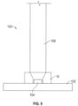
- the light guide assembly 100 includes a PCB 102, an LED 104 mounted on the PCB, a surface-mount device 10 as described, and an optical wave guide 106.
- the solderable support can be partially embedded within the dielectric body using insert molding techniques.
- two solder pad members, one at each end of the device, can be provided with extrusions that are embedded within the dielectric body.
- the surface-mount devices can be installed using conventional surface-mount technology.
- the SMD can be positioned over an electronic component on a circuit board either manually or using a pick-and-place machine.
- a solder paste can be applied to solder pads on the SMD and/or to non-functional solder pads on the PCB to provide temporary fixation of the SMD to the PCB.
- the PCB with attached SMD can be placed in a solder reflow oven and heated to a temperature that melts the solder in the solder paste. After cooling, a strong physical connection is established.
- the electronic component and the SMD can be mounted simultaneously, such as by adhesively or mechanically fixing the electronic component to the SMD to form an assembly that is placed on the PCB and joined thereto using conventional service-mount technology.
Landscapes
- Physics & Mathematics (AREA)
- General Physics & Mathematics (AREA)
- Optics & Photonics (AREA)
- Engineering & Computer Science (AREA)
- Microelectronics & Electronic Packaging (AREA)
- Led Device Packages (AREA)
Claims (10)
- Oberflächenmontierbare Vorrichtung (10), mit:einem dielektrischen Körper (12); undeiner optischen Komponente (24, 26, 28), die auf dem dielektrischen Körper (12) integriert ist,gekennzeichnet durcheine lötbare Metall- oder Metalllegierungs-Halterung (15), die ausgebildet ist, reversibel oder abnehmbar an dem dielektrischen Körper durch eine Rastanordnung verbunden zu werden, wobei die Metall- oder Metalllegierungs-Halterung einen im Wesentlichen rechteckigen Rahmen mit länglichen Elementen (16), quer verlaufenden Lötflächenelementen (18) und einer aufrechtstehenden Klemme (20) mit nach innen zeigenden Lippen (22), die mit Leisten an oberen Enden von Seitenwänden (24) des dielektrischen Körpers (12) im Eingriff sind, aufweist.
- Oberflächenmontierbare Vorrichtung nach Anspruch 1, wobei mindestens eine Durchgangsbohrung in dem dielektrischen Körper (12) ausgebildet ist.
- Oberflächenmontierbare Vorrichtung nach Anspruch 1, wobei der dielektrische Körper (12) ein Kunststoffmaterial aufweist.
- Oberflächenmontierbare Vorrichtung nach Anspruch 1, wobei die lötbare Halterung (15) eine Legierung aus Kupfer aufweist.
- Oberflächenmontierbare Vorrichtung nach Anspruch 1, wobei der dielektrische Körper (12) und die lötbare Halterung (15) ineinander eingerastet sind.
- Oberflächenmontierbare Vorrichtung nach Anspruch 2, wobei die Durchgangsbohrung einen Reflektor zum Fokussieren von Licht bildet, das von einer in einer Vertiefung angeordneten LED (104) ausgesendet wird.
- Oberflächenmontierbare Vorrichtung nach Anspruch 6, wobei Oberflächen (24, 26, 28) des Reflektors mit einer metallisierten Beschichtung versehen sind.
- Oberflächenmontierbare Vorrichtung nach Anspruch 1, wobei die lötbare Metallhalterung (15) eine Klemme ist, die ausgebildet ist, in elastischer Weise mit Elementen des dielektrischen Körpers (12) in Eingriff zu treten.
- Oberflächenmontierbare Vorrichtung nach Anspruch 1, wobei die lötbare Metallhalterung (15) teilweise in den dielektrischen Körper (12) eingebettet ist.
- Oberflächenmontierbare Vorrichtung nach Anspruch 1, wobei die optische Komponente ein Reflektor ist.
Applications Claiming Priority (1)
| Application Number | Priority Date | Filing Date | Title |
|---|---|---|---|
| US16/539,399 US11252821B2 (en) | 2019-08-13 | 2019-08-13 | Optical surface-mount devices |
Publications (2)
| Publication Number | Publication Date |
|---|---|
| EP3792986A1 EP3792986A1 (de) | 2021-03-17 |
| EP3792986B1 true EP3792986B1 (de) | 2023-06-21 |
Family
ID=72046752
Family Applications (1)
| Application Number | Title | Priority Date | Filing Date |
|---|---|---|---|
| EP20190486.9A Active EP3792986B1 (de) | 2019-08-13 | 2020-08-11 | Optische oberflächenmontierte vorrichtungen |
Country Status (2)
| Country | Link |
|---|---|
| US (1) | US11252821B2 (de) |
| EP (1) | EP3792986B1 (de) |
Families Citing this family (2)
| Publication number | Priority date | Publication date | Assignee | Title |
|---|---|---|---|---|
| CN112911824A (zh) * | 2019-12-04 | 2021-06-04 | 菲尼萨公司 | 用于光纤印刷电路板组件的表面安装技术 |
| US20220311510A1 (en) * | 2021-03-24 | 2022-09-29 | M2 Optics, Inc. | Fiber optic link equalization in data centers and other time sensitive applications |
Family Cites Families (20)
| Publication number | Priority date | Publication date | Assignee | Title |
|---|---|---|---|---|
| US4629278A (en) * | 1985-04-15 | 1986-12-16 | Amp Incorporated | Surface mountable connector retention means and method |
| US6940704B2 (en) | 2001-01-24 | 2005-09-06 | Gelcore, Llc | Semiconductor light emitting device |
| AU2003298561A1 (en) | 2002-08-23 | 2004-05-13 | Jonathan S. Dahm | Method and apparatus for using light emitting diodes |
| US7499614B2 (en) * | 2003-10-24 | 2009-03-03 | International Business Machines Corporation | Passive alignment of VCSELs to waveguides in opto-electronic cards and printed circuit boards |
| WO2005067063A1 (en) | 2004-01-12 | 2005-07-21 | Asetronics Ag | Arrangement with a light emitting device on a substrate |
| US7144259B2 (en) * | 2004-02-27 | 2006-12-05 | Finisar Corporation | Optical transceiver module having a dual segment molded lead frame connector |
| WO2006097779A1 (en) * | 2005-03-16 | 2006-09-21 | Infineon Technologies Ag | Substrate, electronic component, electronic configuration and methods of producing the same |
| US7566154B2 (en) | 2006-09-25 | 2009-07-28 | B/E Aerospace, Inc. | Aircraft LED dome light having rotatably releasable housing mounted within mounting flange |
| US20080191335A1 (en) | 2007-02-08 | 2008-08-14 | Advanced Chip Engineering Technology Inc. | Cmos image sensor chip scale package with die receiving opening and method of the same |
| US8172434B1 (en) | 2007-02-23 | 2012-05-08 | DeepSea Power and Light, Inc. | Submersible multi-color LED illumination system |
| EP2477243B1 (de) | 2009-09-11 | 2016-01-06 | Asahi Kasei Chemicals Corporation | Reflektor für eine lichtemittierende vorrichtung und lichtemittierende vorrichtung |
| DE102009053957A1 (de) | 2009-11-19 | 2011-06-01 | Osram Gesellschaft mit beschränkter Haftung | Reflektor für eine Leuchtvorrichtung und Leuchtvorrichtung |
| US9039239B2 (en) * | 2010-02-04 | 2015-05-26 | Sternberg Lanterns, Inc. | Lighting system with lens-retaining structure |
| US8585242B2 (en) | 2010-02-04 | 2013-11-19 | Sternberg Lanterns, Inc. | Lighting system with light-emitting diodes and securing structure |
| US8648359B2 (en) | 2010-06-28 | 2014-02-11 | Cree, Inc. | Light emitting devices and methods |
| EP2587121A1 (de) | 2011-10-28 | 2013-05-01 | Hella KGaA Hueck & Co. | LED-Beleuchtung mit auf der Leiterplatte befestigten Reflektor |
| US9825194B2 (en) | 2012-05-29 | 2017-11-21 | Essence Solar Solutions Ltd. | Self aligning soldering |
| FI20125932A7 (fi) | 2012-09-08 | 2014-03-09 | Lighttherm Oy | Menetelmä LED valaisinlaitteiden valmistamiseksi ja LED valaisinlaitteet |
| US20140191263A1 (en) | 2013-01-07 | 2014-07-10 | Sabic Innovative Plastics Ip B.V. | Compositions for an led reflector and articles thereof |
| EP3078063B1 (de) | 2013-12-06 | 2020-06-10 | Lumileds Holding B.V. | Montageanordnung und beleuchtungsvorrichtung |
-
2019
- 2019-08-13 US US16/539,399 patent/US11252821B2/en active Active
-
2020
- 2020-08-11 EP EP20190486.9A patent/EP3792986B1/de active Active
Also Published As
| Publication number | Publication date |
|---|---|
| US11252821B2 (en) | 2022-02-15 |
| EP3792986A1 (de) | 2021-03-17 |
| US20210051802A1 (en) | 2021-02-18 |
Similar Documents
| Publication | Publication Date | Title |
|---|---|---|
| US5593223A (en) | Illumination device | |
| US8870426B2 (en) | Illumination unit for vehicle headlights and vehicle headlights | |
| US11353186B2 (en) | Vehicular headlight | |
| EP3138734B1 (de) | Lichtmodul, lichtanordnung und rückspiegelvorrichtung für ein fahrzeug | |
| KR20010114154A (ko) | Led 조명장치 및 그 제조방법 | |
| US11757081B2 (en) | Tube lamp with leadframe | |
| CN100359703C (zh) | 辐射构件及其引线框和壳体及带辐射构件的显示装置和/或照明装置 | |
| EP3792986A1 (de) | Optische oberflächenmontierte vorrichtungen | |
| KR102131011B1 (ko) | 카메라 모듈 | |
| US9488773B2 (en) | Circuit board and flat panel display including the same | |
| EP2587124A1 (de) | Led-beleuchtung mit auf der leiterplatte befestigten reflektor | |
| US11892128B2 (en) | Illumination device with leadframe | |
| US7977698B2 (en) | System and method for surface mountable display | |
| US20140286009A1 (en) | Modular solid state electronic display panels with electromagnetic radiation shielding | |
| JP4937241B2 (ja) | Led光源及びその製造方法 | |
| KR20100067818A (ko) | 샤시 베이스 및 이를 구비한 플라즈마 디스플레이 장치 | |
| JP2018508115A (ja) | Ledランプ用フレキシブル回路基板組立体 | |
| JP5080843B2 (ja) | 表面実装用スタンド、表面実装型ledランプ及びledユニット | |
| TWI627798B (zh) | 具有照明發光二極體之電路 | |
| JP5225273B2 (ja) | 光学要素と位置合わせされた電子−光学部品の取り付け | |
| EP1949461B1 (de) | Verfahren zur herstellung eines zusammenbaus von beleuchtungselementen auf einem substrat | |
| KR20070066035A (ko) | 발광다이오드 실장용 플렉시블 금속회로기판 및 그제조방법 | |
| KR101133184B1 (ko) | 엘이디 램프의 제조방법 | |
| KR101582788B1 (ko) | 인쇄회로기판, 이를 포함하는 조명모듈 및 상기 조명모듈의 제조방법 | |
| KR101294505B1 (ko) | 방열회로기판 및 그를 포함하는 샤시 구조물 |
Legal Events
| Date | Code | Title | Description |
|---|---|---|---|
| PUAI | Public reference made under article 153(3) epc to a published international application that has entered the european phase |
Free format text: ORIGINAL CODE: 0009012 |
|
| STAA | Information on the status of an ep patent application or granted ep patent |
Free format text: STATUS: THE APPLICATION HAS BEEN PUBLISHED |
|
| AK | Designated contracting states |
Kind code of ref document: A1 Designated state(s): AL AT BE BG CH CY CZ DE DK EE ES FI FR GB GR HR HU IE IS IT LI LT LU LV MC MK MT NL NO PL PT RO RS SE SI SK SM TR |
|
| AX | Request for extension of the european patent |
Extension state: BA ME |
|
| STAA | Information on the status of an ep patent application or granted ep patent |
Free format text: STATUS: REQUEST FOR EXAMINATION WAS MADE |
|
| 17P | Request for examination filed |
Effective date: 20210916 |
|
| RBV | Designated contracting states (corrected) |
Designated state(s): AL AT BE BG CH CY CZ DE DK EE ES FI FR GB GR HR HU IE IS IT LI LT LU LV MC MK MT NL NO PL PT RO RS SE SI SK SM TR |
|
| STAA | Information on the status of an ep patent application or granted ep patent |
Free format text: STATUS: EXAMINATION IS IN PROGRESS |
|
| 17Q | First examination report despatched |
Effective date: 20220419 |
|
| GRAP | Despatch of communication of intention to grant a patent |
Free format text: ORIGINAL CODE: EPIDOSNIGR1 |
|
| STAA | Information on the status of an ep patent application or granted ep patent |
Free format text: STATUS: GRANT OF PATENT IS INTENDED |
|
| RIC1 | Information provided on ipc code assigned before grant |
Ipc: H01L 33/60 20100101ALI20221206BHEP Ipc: H01L 25/075 20060101ALI20221206BHEP Ipc: H01L 33/62 20100101ALI20221206BHEP Ipc: H01L 33/48 20100101ALI20221206BHEP Ipc: F21V 8/00 20060101ALI20221206BHEP Ipc: H01L 33/00 20100101AFI20221206BHEP |
|
| INTG | Intention to grant announced |
Effective date: 20230103 |
|
| GRAS | Grant fee paid |
Free format text: ORIGINAL CODE: EPIDOSNIGR3 |
|
| GRAA | (expected) grant |
Free format text: ORIGINAL CODE: 0009210 |
|
| STAA | Information on the status of an ep patent application or granted ep patent |
Free format text: STATUS: THE PATENT HAS BEEN GRANTED |
|
| AK | Designated contracting states |
Kind code of ref document: B1 Designated state(s): AL AT BE BG CH CY CZ DE DK EE ES FI FR GB GR HR HU IE IS IT LI LT LU LV MC MK MT NL NO PL PT RO RS SE SI SK SM TR |
|
| REG | Reference to a national code |
Ref country code: CH Ref legal event code: EP |
|
| REG | Reference to a national code |
Ref country code: DE Ref legal event code: R096 Ref document number: 602020012693 Country of ref document: DE |
|
| REG | Reference to a national code |
Ref country code: AT Ref legal event code: REF Ref document number: 1581545 Country of ref document: AT Kind code of ref document: T Effective date: 20230715 |
|
| REG | Reference to a national code |
Ref country code: IE Ref legal event code: FG4D |
|
| REG | Reference to a national code |
Ref country code: LT Ref legal event code: MG9D |
|
| REG | Reference to a national code |
Ref country code: NL Ref legal event code: MP Effective date: 20230621 |
|
| PG25 | Lapsed in a contracting state [announced via postgrant information from national office to epo] |
Ref country code: SE Free format text: LAPSE BECAUSE OF FAILURE TO SUBMIT A TRANSLATION OF THE DESCRIPTION OR TO PAY THE FEE WITHIN THE PRESCRIBED TIME-LIMIT Effective date: 20230621 Ref country code: NO Free format text: LAPSE BECAUSE OF FAILURE TO SUBMIT A TRANSLATION OF THE DESCRIPTION OR TO PAY THE FEE WITHIN THE PRESCRIBED TIME-LIMIT Effective date: 20230921 |
|
| REG | Reference to a national code |
Ref country code: AT Ref legal event code: MK05 Ref document number: 1581545 Country of ref document: AT Kind code of ref document: T Effective date: 20230621 |
|
| PG25 | Lapsed in a contracting state [announced via postgrant information from national office to epo] |
Ref country code: RS Free format text: LAPSE BECAUSE OF FAILURE TO SUBMIT A TRANSLATION OF THE DESCRIPTION OR TO PAY THE FEE WITHIN THE PRESCRIBED TIME-LIMIT Effective date: 20230621 Ref country code: NL Free format text: LAPSE BECAUSE OF FAILURE TO SUBMIT A TRANSLATION OF THE DESCRIPTION OR TO PAY THE FEE WITHIN THE PRESCRIBED TIME-LIMIT Effective date: 20230621 Ref country code: LV Free format text: LAPSE BECAUSE OF FAILURE TO SUBMIT A TRANSLATION OF THE DESCRIPTION OR TO PAY THE FEE WITHIN THE PRESCRIBED TIME-LIMIT Effective date: 20230621 Ref country code: LT Free format text: LAPSE BECAUSE OF FAILURE TO SUBMIT A TRANSLATION OF THE DESCRIPTION OR TO PAY THE FEE WITHIN THE PRESCRIBED TIME-LIMIT Effective date: 20230621 Ref country code: HR Free format text: LAPSE BECAUSE OF FAILURE TO SUBMIT A TRANSLATION OF THE DESCRIPTION OR TO PAY THE FEE WITHIN THE PRESCRIBED TIME-LIMIT Effective date: 20230621 Ref country code: GR Free format text: LAPSE BECAUSE OF FAILURE TO SUBMIT A TRANSLATION OF THE DESCRIPTION OR TO PAY THE FEE WITHIN THE PRESCRIBED TIME-LIMIT Effective date: 20230922 |
|
| PG25 | Lapsed in a contracting state [announced via postgrant information from national office to epo] |
Ref country code: FI Free format text: LAPSE BECAUSE OF FAILURE TO SUBMIT A TRANSLATION OF THE DESCRIPTION OR TO PAY THE FEE WITHIN THE PRESCRIBED TIME-LIMIT Effective date: 20230621 |
|
| PG25 | Lapsed in a contracting state [announced via postgrant information from national office to epo] |
Ref country code: SK Free format text: LAPSE BECAUSE OF FAILURE TO SUBMIT A TRANSLATION OF THE DESCRIPTION OR TO PAY THE FEE WITHIN THE PRESCRIBED TIME-LIMIT Effective date: 20230621 |
|
| PG25 | Lapsed in a contracting state [announced via postgrant information from national office to epo] |
Ref country code: ES Free format text: LAPSE BECAUSE OF FAILURE TO SUBMIT A TRANSLATION OF THE DESCRIPTION OR TO PAY THE FEE WITHIN THE PRESCRIBED TIME-LIMIT Effective date: 20230621 |
|
| PG25 | Lapsed in a contracting state [announced via postgrant information from national office to epo] |
Ref country code: IS Free format text: LAPSE BECAUSE OF FAILURE TO SUBMIT A TRANSLATION OF THE DESCRIPTION OR TO PAY THE FEE WITHIN THE PRESCRIBED TIME-LIMIT Effective date: 20231021 |
|
| PG25 | Lapsed in a contracting state [announced via postgrant information from national office to epo] |
Ref country code: SM Free format text: LAPSE BECAUSE OF FAILURE TO SUBMIT A TRANSLATION OF THE DESCRIPTION OR TO PAY THE FEE WITHIN THE PRESCRIBED TIME-LIMIT Effective date: 20230621 Ref country code: SK Free format text: LAPSE BECAUSE OF FAILURE TO SUBMIT A TRANSLATION OF THE DESCRIPTION OR TO PAY THE FEE WITHIN THE PRESCRIBED TIME-LIMIT Effective date: 20230621 Ref country code: RO Free format text: LAPSE BECAUSE OF FAILURE TO SUBMIT A TRANSLATION OF THE DESCRIPTION OR TO PAY THE FEE WITHIN THE PRESCRIBED TIME-LIMIT Effective date: 20230621 Ref country code: PT Free format text: LAPSE BECAUSE OF FAILURE TO SUBMIT A TRANSLATION OF THE DESCRIPTION OR TO PAY THE FEE WITHIN THE PRESCRIBED TIME-LIMIT Effective date: 20231023 Ref country code: IS Free format text: LAPSE BECAUSE OF FAILURE TO SUBMIT A TRANSLATION OF THE DESCRIPTION OR TO PAY THE FEE WITHIN THE PRESCRIBED TIME-LIMIT Effective date: 20231021 Ref country code: ES Free format text: LAPSE BECAUSE OF FAILURE TO SUBMIT A TRANSLATION OF THE DESCRIPTION OR TO PAY THE FEE WITHIN THE PRESCRIBED TIME-LIMIT Effective date: 20230621 Ref country code: EE Free format text: LAPSE BECAUSE OF FAILURE TO SUBMIT A TRANSLATION OF THE DESCRIPTION OR TO PAY THE FEE WITHIN THE PRESCRIBED TIME-LIMIT Effective date: 20230621 Ref country code: CZ Free format text: LAPSE BECAUSE OF FAILURE TO SUBMIT A TRANSLATION OF THE DESCRIPTION OR TO PAY THE FEE WITHIN THE PRESCRIBED TIME-LIMIT Effective date: 20230621 Ref country code: AT Free format text: LAPSE BECAUSE OF FAILURE TO SUBMIT A TRANSLATION OF THE DESCRIPTION OR TO PAY THE FEE WITHIN THE PRESCRIBED TIME-LIMIT Effective date: 20230621 |
|
| PG25 | Lapsed in a contracting state [announced via postgrant information from national office to epo] |
Ref country code: PL Free format text: LAPSE BECAUSE OF FAILURE TO SUBMIT A TRANSLATION OF THE DESCRIPTION OR TO PAY THE FEE WITHIN THE PRESCRIBED TIME-LIMIT Effective date: 20230621 |
|
| PG25 | Lapsed in a contracting state [announced via postgrant information from national office to epo] |
Ref country code: MC Free format text: LAPSE BECAUSE OF FAILURE TO SUBMIT A TRANSLATION OF THE DESCRIPTION OR TO PAY THE FEE WITHIN THE PRESCRIBED TIME-LIMIT Effective date: 20230621 |
|
| REG | Reference to a national code |
Ref country code: DE Ref legal event code: R097 Ref document number: 602020012693 Country of ref document: DE |
|
| REG | Reference to a national code |
Ref country code: CH Ref legal event code: PL |
|
| PG25 | Lapsed in a contracting state [announced via postgrant information from national office to epo] |
Ref country code: MC Free format text: LAPSE BECAUSE OF FAILURE TO SUBMIT A TRANSLATION OF THE DESCRIPTION OR TO PAY THE FEE WITHIN THE PRESCRIBED TIME-LIMIT Effective date: 20230621 |
|
| PG25 | Lapsed in a contracting state [announced via postgrant information from national office to epo] |
Ref country code: LU Free format text: LAPSE BECAUSE OF NON-PAYMENT OF DUE FEES Effective date: 20230811 |
|
| PLBE | No opposition filed within time limit |
Free format text: ORIGINAL CODE: 0009261 |
|
| STAA | Information on the status of an ep patent application or granted ep patent |
Free format text: STATUS: NO OPPOSITION FILED WITHIN TIME LIMIT |
|
| PG25 | Lapsed in a contracting state [announced via postgrant information from national office to epo] |
Ref country code: LU Free format text: LAPSE BECAUSE OF NON-PAYMENT OF DUE FEES Effective date: 20230811 Ref country code: DK Free format text: LAPSE BECAUSE OF FAILURE TO SUBMIT A TRANSLATION OF THE DESCRIPTION OR TO PAY THE FEE WITHIN THE PRESCRIBED TIME-LIMIT Effective date: 20230621 Ref country code: CH Free format text: LAPSE BECAUSE OF NON-PAYMENT OF DUE FEES Effective date: 20230831 |
|
| PG25 | Lapsed in a contracting state [announced via postgrant information from national office to epo] |
Ref country code: SI Free format text: LAPSE BECAUSE OF FAILURE TO SUBMIT A TRANSLATION OF THE DESCRIPTION OR TO PAY THE FEE WITHIN THE PRESCRIBED TIME-LIMIT Effective date: 20230621 |
|
| REG | Reference to a national code |
Ref country code: BE Ref legal event code: MM Effective date: 20230831 |
|
| REG | Reference to a national code |
Ref country code: IE Ref legal event code: MM4A |
|
| 26N | No opposition filed |
Effective date: 20240322 |
|
| PG25 | Lapsed in a contracting state [announced via postgrant information from national office to epo] |
Ref country code: SI Free format text: LAPSE BECAUSE OF FAILURE TO SUBMIT A TRANSLATION OF THE DESCRIPTION OR TO PAY THE FEE WITHIN THE PRESCRIBED TIME-LIMIT Effective date: 20230621 Ref country code: IT Free format text: LAPSE BECAUSE OF FAILURE TO SUBMIT A TRANSLATION OF THE DESCRIPTION OR TO PAY THE FEE WITHIN THE PRESCRIBED TIME-LIMIT Effective date: 20230621 |
|
| PG25 | Lapsed in a contracting state [announced via postgrant information from national office to epo] |
Ref country code: IE Free format text: LAPSE BECAUSE OF NON-PAYMENT OF DUE FEES Effective date: 20230811 |
|
| PG25 | Lapsed in a contracting state [announced via postgrant information from national office to epo] |
Ref country code: IE Free format text: LAPSE BECAUSE OF NON-PAYMENT OF DUE FEES Effective date: 20230811 Ref country code: FR Free format text: LAPSE BECAUSE OF NON-PAYMENT OF DUE FEES Effective date: 20230821 |
|
| PG25 | Lapsed in a contracting state [announced via postgrant information from national office to epo] |
Ref country code: BE Free format text: LAPSE BECAUSE OF NON-PAYMENT OF DUE FEES Effective date: 20230831 |
|
| PG25 | Lapsed in a contracting state [announced via postgrant information from national office to epo] |
Ref country code: BG Free format text: LAPSE BECAUSE OF FAILURE TO SUBMIT A TRANSLATION OF THE DESCRIPTION OR TO PAY THE FEE WITHIN THE PRESCRIBED TIME-LIMIT Effective date: 20230621 |
|
| REG | Reference to a national code |
Ref country code: DE Ref legal event code: R079 Ref document number: 602020012693 Country of ref document: DE Free format text: PREVIOUS MAIN CLASS: H01L0033000000 Ipc: H10H0020000000 |
|
| PG25 | Lapsed in a contracting state [announced via postgrant information from national office to epo] |
Ref country code: BG Free format text: LAPSE BECAUSE OF FAILURE TO SUBMIT A TRANSLATION OF THE DESCRIPTION OR TO PAY THE FEE WITHIN THE PRESCRIBED TIME-LIMIT Effective date: 20230621 |
|
| GBPC | Gb: european patent ceased through non-payment of renewal fee |
Effective date: 20240811 |
|
| PG25 | Lapsed in a contracting state [announced via postgrant information from national office to epo] |
Ref country code: GB Free format text: LAPSE BECAUSE OF NON-PAYMENT OF DUE FEES Effective date: 20240811 |
|
| PG25 | Lapsed in a contracting state [announced via postgrant information from national office to epo] |
Ref country code: CY Free format text: LAPSE BECAUSE OF FAILURE TO SUBMIT A TRANSLATION OF THE DESCRIPTION OR TO PAY THE FEE WITHIN THE PRESCRIBED TIME-LIMIT; INVALID AB INITIO Effective date: 20200811 |
|
| PG25 | Lapsed in a contracting state [announced via postgrant information from national office to epo] |
Ref country code: HU Free format text: LAPSE BECAUSE OF FAILURE TO SUBMIT A TRANSLATION OF THE DESCRIPTION OR TO PAY THE FEE WITHIN THE PRESCRIBED TIME-LIMIT; INVALID AB INITIO Effective date: 20200811 |
|
| PGFP | Annual fee paid to national office [announced via postgrant information from national office to epo] |
Ref country code: DE Payment date: 20250827 Year of fee payment: 6 |
|
| PG25 | Lapsed in a contracting state [announced via postgrant information from national office to epo] |
Ref country code: TR Free format text: LAPSE BECAUSE OF FAILURE TO SUBMIT A TRANSLATION OF THE DESCRIPTION OR TO PAY THE FEE WITHIN THE PRESCRIBED TIME-LIMIT Effective date: 20230621 |