EP3789830A1 - Cadran et procédé de fabrication d'un cadran pour une montre - Google Patents
Cadran et procédé de fabrication d'un cadran pour une montre Download PDFInfo
- Publication number
- EP3789830A1 EP3789830A1 EP19196181.2A EP19196181A EP3789830A1 EP 3789830 A1 EP3789830 A1 EP 3789830A1 EP 19196181 A EP19196181 A EP 19196181A EP 3789830 A1 EP3789830 A1 EP 3789830A1
- Authority
- EP
- European Patent Office
- Prior art keywords
- layer
- dial
- photovoltaic
- transparent
- decorative
- Prior art date
- Legal status (The legal status is an assumption and is not a legal conclusion. Google has not performed a legal analysis and makes no representation as to the accuracy of the status listed.)
- Granted
Links
Images



Classifications
-
- G—PHYSICS
- G04—HOROLOGY
- G04C—ELECTROMECHANICAL CLOCKS OR WATCHES
- G04C10/00—Arrangements of electric power supplies in time-pieces
- G04C10/02—Arrangements of electric power supplies in time-pieces the power supply being a radioactive or photovoltaic source
-
- G—PHYSICS
- G04—HOROLOGY
- G04B—MECHANICALLY-DRIVEN CLOCKS OR WATCHES; MECHANICAL PARTS OF CLOCKS OR WATCHES IN GENERAL; TIME PIECES USING THE POSITION OF THE SUN, MOON OR STARS
- G04B19/00—Indicating the time by visual means
- G04B19/06—Dials
- G04B19/10—Ornamental shape of the graduations or the surface of the dial; Attachment of the graduations to the dial
-
- G—PHYSICS
- G04—HOROLOGY
- G04B—MECHANICALLY-DRIVEN CLOCKS OR WATCHES; MECHANICAL PARTS OF CLOCKS OR WATCHES IN GENERAL; TIME PIECES USING THE POSITION OF THE SUN, MOON OR STARS
- G04B19/00—Indicating the time by visual means
- G04B19/06—Dials
-
- Y—GENERAL TAGGING OF NEW TECHNOLOGICAL DEVELOPMENTS; GENERAL TAGGING OF CROSS-SECTIONAL TECHNOLOGIES SPANNING OVER SEVERAL SECTIONS OF THE IPC; TECHNICAL SUBJECTS COVERED BY FORMER USPC CROSS-REFERENCE ART COLLECTIONS [XRACs] AND DIGESTS
- Y02—TECHNOLOGIES OR APPLICATIONS FOR MITIGATION OR ADAPTATION AGAINST CLIMATE CHANGE
- Y02E—REDUCTION OF GREENHOUSE GAS [GHG] EMISSIONS, RELATED TO ENERGY GENERATION, TRANSMISSION OR DISTRIBUTION
- Y02E10/00—Energy generation through renewable energy sources
- Y02E10/50—Photovoltaic [PV] energy
- Y02E10/542—Dye sensitized solar cells
Definitions
- the invention relates to watch dials, more particularly watch dials comprising a photovoltaic layer.
- the document JP 2005346934 aims to provide a dye sensitized solar cell.
- the document proposes a solar cell 11 sensitized by a dye equipped with an upper flat glass g1, a lower flat glass g2 facing the upper flat glass.
- a first layer 111 sensitized to the dye is disposed in a first region E1 between the upper flat glass and the lower flat glass.
- a second layer 112 sensitized by a dye is disposed in a second region E2 different from the first region E1.
- the regions E1 and E2 are located between the upper flat glass and the lower flat glass.
- the second layer 112 has a different color from that of the first layer 111.
- the document JP 2005324517 aims to provide a decorative device.
- the decorative device is equipped with a dye sensitized solar cell 11 disposed in a region between a pair of light transmitting substrates (eg, a glass top plate (g1) and a glass bottom plate (g2)).
- a decorative part 13 is provided to at least one of the pair of the light transmitting substrates.
- a dial is the part of a watch that displays the time by means of one or more time markers (e.g. indication of a number (12 or XII, 60, ...)) and hands in movement.
- time markers e.g. indication of a number (12 or XII, 60, ...)
- the periphery of the dial is numbered from 1 to 12 and indicates the hours on a 12-hour cycle.
- a first hand makes one revolution every 12 hours.
- One or more holes are made in the dial for the passage of one or more axes of one or more hands.
- a first aspect of the invention relates to a dial for a watch.
- the dial comprises a semi-transparent photovoltaic layer having a lower face.
- the dial also comprises a decorative ink-based layer printed on the underside of the photovoltaic layer.
- the decorative layer comprises a pattern comprising one or more time markers.
- photovoltaic layer is understood to mean a layer which, when exposed to light, produces electricity by virtue of the photovoltaic effect.
- semi-transparent layer is understood to mean a layer comprising one or more transparent zones and one or more opaque zones, the layer being, in terms of surface, predominantly transparent.
- the surface of the one or more transparent zones is greater than 80%, preferably included in a range going from 80% to 95%, of the surface of the layer.
- the expression “upper”, “top” or “top” face, surface or side of an object is understood to mean the face, surface or side of the object closest to the user of the device. watch. It is also about the face, surface or side of the object receiving the incident light. Conversely, by face, surface or side “lower”, “from below” or “bottom” of an object, the face, surface or side of the object furthest from the eyes of the user. watch (i.e. face, surface or side opposite to the face, surface or top side).
- ink is meant a liquid (or possibly a paste) containing one or more pigments or one or more dyes and serving to color a surface in order to produce p. ex. an image, a text or a drawing.
- time mark any element making it possible to infer the current time using one or more hands of the watch (eg indication of a number (12 or XII, 60, etc.) on the periphery of the clock. dial).
- the present invention makes it possible to reduce the number of parts necessary for mounting the dial due to the fact that the decorative layer is printed on the photovoltaic layer (the decorative layer and the photovoltaic layer are integral and do not require attachment in situ when of the watch assembly).
- the pattern preferably comprises a first area comprising a first ink and a second area comprising a second ink.
- the first ink and the second ink being different.
- the first zone is central and the second zone is peripheral.
- different ink is meant an ink having a different chemical composition from another ink.
- the decorative layer can be opaque or semi-transparent. It can be plain or have several patterns with or without symmetry. It will be appreciated that great freedom is allowed in terms of decoration patterns.
- the semi-transparent photovoltaic layer comprises an arrangement of one or more photovoltaic cells covering between 5% and 20%, preferably between 7% and 15%, even more preferably between 9% and 11% of the surface. diaper photovoltaic. It will be appreciated that in this way a majority of the incident light illuminates the decorative layer.
- the one or more photovoltaic cells are arranged in a network, the network preferably being a hexagonal, linear, or triangular network.
- the network is a mixed network comprising at least two of the following networks: a hexagonal network, a linear network and a triangular network.
- the network could be irregular.
- the photovoltaic layer comprises a protective sublayer (optionally transparent or semi-transparent), the protective sublayer being the lower layer of the photovoltaic layer and being in contact with the decorative layer.
- a protective sublayer optionally transparent or semi-transparent
- the dial comprises a shiny transparent layer arranged between the semi-transparent photovoltaic layer and the decorative layer.
- the photovoltaic layer comprises an active material having a different sensitivity depending on the wavelength of the incident light.
- the decorative layer is configured to reflect incident light at a wavelength substantially equal to a maximum sensitivity of the active material.
- the decorative layer is configured to reflect incident light at a wavelength in a range of -150 nm to 150 nm, more preferably in a range of -100 nm to 100 nm, still more preferably in a range of -150 nm to 150 nm, more preferably in a range of -100 nm to 100 nm, still more preferably in a range of -100 nm to 100 nm. range from -50 nm to 50 nm centered on a maximum sensitivity of the active material.
- sensitivity of a photovoltaic active material to a wavelength is understood to mean the capacity of this material to absorb a wave incident at this wavelength and to transform it, by the photovoltaic effect, into electrical energy.
- a second aspect of the invention relates to a method of manufacturing a dial for a watch.
- the method includes providing a semi-transparent photovoltaic layer having a bottom face.
- the method further comprises applying a decorative ink-based layer to the underside of the photovoltaic layer.
- the decorative layer comprises a pattern comprising one or more time markers.
- the application of the decorative layer is carried out by printing.
- the application of the decorative layer is carried out by digital printing.
- the pattern can be applied according to an application plan recorded in a digital printer performing digital printing.
- the printing is carried out by a UV flatbed printer.
- the method comprises the application of a glossy transparent layer, the top finishing layer being applied between the semi-transparent photovoltaic layer and the decorative layer.
- a third aspect of the invention relates to a watch comprising the dial according to the first aspect of the invention.
- the Fig. 1 shows a cross section of a dial 2 of a watch according to a preferred embodiment of the invention.
- the dial 2 comprises, from the top to the bottom of the dial, a semi-transparent photovoltaic layer 6, a shiny transparent layer 4 and a decorative layer 8.
- the top of the dial is understood to mean the part closest to the eyes of the user of the dial. the watch.
- the uppermost layer is also the layer first passed through by incident light 10.
- the semi-transparent photovoltaic layer 6 comprises a transparent glass sublayer 12, one or more photovoltaic cells 14 arranged in a hexagonal array and a protective sublayer 16.
- the protective sublayer 16 structurally stabilizes the hexagonal array of photovoltaic cells 14 and protects it against possible shocks.
- the protective sublayer 16 is in direct contact with the glossy transparent layer 4, in particular, the lower face of the protective sublayer 16 of the photovoltaic layer is in direct contact with the upper layer of the glossy transparent layer 4.
- the active material used for the one or more photovoltaic cells 14 is based on amorphous silicon. It will be appreciated, however, that according to other embodiments, the active material may be different.
- the transparent glass sublayer 12 can be replaced by an sublayer of another transparent material (possibly partially transparent) such as p. ex. sapphire or plastic.
- the hexagonal array of photovoltaic cells 14 covers between 5% and 20%, preferably between 7% and 15%, even more preferably between 9% and 11% of the surface of the photovoltaic layer. He It will be appreciated that in this way a majority of the incident light 10 illuminates the decorative layer 8.
- the decorative layer 8 is applied to the semi-transparent photovoltaic layer 6, by digital printing.
- the decorative layer 8 comprises a pattern 18 comprising several time marks 20.
- the decorative layer 8 can be colored p. ex. in black, white, yellow, purple, etc., and possibly include transparent areas. It will be appreciated that digital printing provides great flexibility in the patterns printed. Printing can be performed by a UV flatbed printer. The pattern can be applied according to an application plan recorded in a digital printer performing digital printing.
- the pattern may include a plurality of areas comprising different inks.
- the decorative layer 8 can comprise a first zone 22 comprising a first ink and a second zone 24 comprising a second ink.
- the first ink and the second ink are different in the sense that they have p. ex. another chemical composition and / or another color.
- the temporal markers 20 can for example be indicated by the second zone 24.
- the transparent layer 4 is placed between the semi-transparent photovoltaic layer 6 and the decorative layer 8.
- the transparent layer 4 can improve the interface between the ink of the decorative layer and the photovoltaic layer 6, p. ex. in the event of a physical and / or chemical incompatibility between the ink of the decorative layer 8 and the photovoltaic layer 6.
- the decorative layer 8 comprises a first black central zone 22.
- the first zone 22 comprises four time marks each indicated by a point associated with the numbers “12”, “3”, “6” and “9” indicated in white.
- the first zone 22 is surrounded by a peripheral zone 24 of purple color.
- the pattern of the peripheral zone 24 also includes marks temporal form of a rosette whose tips are separated from it by a 60th revolution.
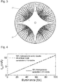
- FIG. 3 A second example of a pattern is shown on Fig. 3 .
- the second example is identical to the first except for the choice of colors.
- the first central zone 22 is inkless, semi-transparent (the numbers being black) and the second peripheral zone 24 is yellow.
- the semi-transparent photovoltaic layer comprises an array of one or more photovoltaic cells covering 10% of the surface of the photovoltaic layer.
- the printing of the decorative layer is carried out by a UV flatbed printer.
- the current at zero voltage Isc is proportional to the illuminance received by the sample.
- the graphics shown in Figs. 4 and 5 represent typical results of the current at zero voltage Isc as a function of the illuminance.
- the Fig. 4 corresponds to the comparison between a sample with (broken line) or without (solid line) black and purple decorative layer comprising a hexagonal array of photovoltaic cells covering 10% of the surface of the photovoltaic layer.
- the slopes obtained are respectively 0.113 mA / klx and 0.111 mA / klx.
- the zero voltage current Isc is only slightly affected by the application of a purple decorative layer, it is even increased by approximately 2%. In the case of the application of a yellow decorative layer, the intensity at zero voltage Isc has increased by 15%.
- the photovoltaic efficiency can be improved depending on the colors chosen for the decorative layer.
- the improvement is due to the light backscattered at the glass-printed layer interface and undergoing multiple reflections inside the glass underlayer. The light thus reflected improves the efficiency since an additional part of the incident light reaches the one or more photovoltaic cells. In the absence of a decorative layer, this additional part is lost because it is not reflected and therefore does not reach the one or more photovoltaic cells.
- the Fig. 6 shows the results of a simulation (Ray Tracing Simulation) for a sample without decorative layer (circles) and with white decorative layer (cross).
- Incident light 10 is characterized by a solar spectrum.
- the white decorative layer is modeled by a Lambertian surface without absorption.
- the graph represents the illumination of the photovoltaic layer 14 as a function of the surface fill factor of between 1% and 100%. The difference between the two samples is represented by squares.
- the Fig. 7 represents the relative increase in the light incident on the photovoltaic layer 14 as a function of the surface filling factor of between 1% and 100%. This curve represents the maximum increase in illumination on the photovoltaic layers due to the light backscattered at the glass-printed layer interface and undergoing multiple reflections inside the glass underlayer since in these simulations, a Zero absorption of the decorative layer 8 and of the glass 12 was considered.
- the Fig. 8 represents the sensitivity curve of the active material (amorphous silicon) as a function of the wavelength of the incident light.
- the visible colors are also represented as a function of the wavelength.
- the maximum sensitivity (1 in arbitrary units) of the active material is around 525 nm (green).
- the sensibility of the material to the yellow color is approximately 0.9 (i.e. 90% of the maximum sensitivity of the active material).
- the sensitivity of the material to the color violet is approximately 0.55 (i.e. 55% of the maximum sensitivity of the active material). It follows, therefore, that it is more beneficial to reflect generally yellow light (i.e. have a generally yellow decorative layer) than to reflect generally purple light (i.e. have a decorative layer generally purple) in the case of amorphous silicon.
- the yield can be increased by increasing the proportion of the surface of white color (reflection of substantially all the colors composing the incident light) with respect to the total surface of the decorative layer. or by increasing the proportion of colors whose wavelength is close to the maximum spectral sensitivity of the active material (450 to 600 nm, blue to orange in the case of amorphous silicon).
- fluorescent inks absorbing outside the maximum sensitivity and emitting near the maximum sensitivity of the active material, could also improve performance.
- the choice could be made for an ink which absorbs in the ultraviolet range and emits in the visible range.
- the emission of this fluorescence could take place at a wavelength within an interval ranging from -150 nm to 150 nm centered on a maximum sensitivity of the active material.
Landscapes
- Physics & Mathematics (AREA)
- General Physics & Mathematics (AREA)
- Engineering & Computer Science (AREA)
- Power Engineering (AREA)
- Photovoltaic Devices (AREA)
- Electric Clocks (AREA)
Abstract
Description
- De manière générale, l'invention concerne des cadrans de montre, plus particulièrement des cadrans de montre comprenant une couche photovoltaïque.
- Le document
JP 2005346934 - Le document
JP 2005324517 - La publication scientifique L. Wen et. al, « Theoretical design of multi-colored semi-transparent organic solar cells with both efficient color filtering and light harvesting » Sci. Rep. 4 (2014) rapporte une cellule solaire incorporant une capacité de coloration multiple offrant une solution esthétique et ouvrant la possibilité d'un affichage coloré auto-alimenté.
- Un cadran est la partie d'une montre qui affiche l'heure au moyen d'un ou plusieurs repères temporels (p. ex. indication d'un nombre (12 ou XII, 60, ...)) et d'aiguilles en mouvement. Dans sa forme la plus élémentaire, la périphérie du cadran est numérotée de 1 à 12 et indique les heures sur un cycle de 12 heures. Une première aiguille fait une révolution toutes les 12 heures. Une seconde aiguille, plus longue que la première aiguille fait une révolution par heure. Un ou plusieurs trous sont ménagés dans le cadran pour le passage d'un ou plusieurs axes des une ou plusieurs aiguilles.
- Un premier aspect de l'invention concerne un cadran pour une montre Le cadran comprend une couche photovoltaïque semi-transparente ayant une face inférieure. D'autre part le cadran comprend aussi une couche décorative à base d'encre imprimée sur la face inférieure de la couche photovoltaïque. La couche décorative comprend un motif comprenant un ou plusieurs repères temporels.
- On entend par « couche photovoltaïque », une couche qui, exposée à la lumière, produit de l'électricité grâce à l'effet photovoltaïque.
- Par couche « semi-transparente », on entend une couche comprenant une ou plusieurs zones transparentes et une ou plusieurs zones opaques, la couche étant, en terme de surface, majoritairement transparente. Préférablement la surface des une ou plusieurs zones transparentes est supérieure à 80%, préférablement comprise dans un intervalle allant de 80% à 95%, de la surface de la couche.
- D'une façon générale, on entend par face, surface ou côté « supérieur », « du dessus » ou « haut » d'un objet, la face, surface ou côté de l'objet le plus proche de l'utilisateur de la montre. Il s'agit aussi de la face, surface ou côté de l'objet recevant la lumière incidente. A l'inverse, on entend par face, surface ou côté « inférieur », « du dessous » ou « bas » d'un objet, la face, surface ou côté de l'objet le plus éloigné des yeux de l'utilisateur de la montre (c.-à-d. la face, surface ou côté opposé à la face, surface ou côté supérieur).
- Par « encre », on entend un liquide (ou éventuellement une pâte) contenant un ou plusieurs pigments ou un ou plusieurs colorants et servant à colorer une surface afin de produire p. ex. une image, un texte ou un dessin.
- Par « repère temporel » on entend tout élément permettant d'inférer l'heure actuelle grâce aux une ou plusieurs aiguilles de la montre (p. ex. indication d'un nombre (12 ou XII, 60, ...) en périphérie du cadran).
- Il sera apprécié que la présente invention permette de réduire le nombre de pièces nécessaires au montage du cadran du fait que la couche décorative est imprimée sur la couche photovoltaïque (la couche décorative et la couche photovoltaïque sont solidaires et ne nécessitent pas une solidarisation in situ lors du montage de la montre).
- Le motif comprend préférablement une première zone comprenant une première encre et une seconde zone comprenant une seconde encre. La première encre et la seconde encre étant différentes. Préférablement la première zone est centrale et la seconde zone est périphérique. Par encre différente, on entend une encre ayant une composition chimique différente d'une autre encre. La couche décorative peut être opaque ou semi-transparente. Elle peut être unie ou comporter plusieurs motifs avec ou sans symétrie. Il sera apprécié qu'une grande liberté est permise au niveau des motifs de décoration.
- Selon un mode de réalisation, la couche photovoltaïque semi-transparente comprend un arrangement d'une ou plusieurs cellules photovoltaïques couvrant entre 5% et 20%, préférablement entre 7% et 15%, encore plus préférablement entre 9% et 11% de la surface de couche photovoltaïque. Il sera apprécié que, de cette façon, une majorité de la lumière incidente illumine la couche décorative.
- Selon un mode de réalisation, les une ou plusieurs cellules photovoltaïques sont arrangées selon un réseau, le réseau étant préférablement un réseau hexagonal, linéaire, ou triangulaire. Selon un autre mode de réalisation, le réseau est un réseau mixte comprenant au moins deux des réseaux suivants : un réseau hexagonal, un réseau linéaire et un réseau triangulaire. Selon un autre mode de réalisation, le réseau pourrait être irrégulier.
- Préférablement, la couche photovoltaïque comprend une sous couche protectrice (éventuellement transparente ou semi-transparente), la sous couche protectrice étant la couche inférieure de la couche photovoltaïque et étant en contact avec la couche décorative.
- Selon un mode de réalisation préféré, le cadran comprend une couche transparente brillante disposée entre la couche photovoltaïque semi-transparente et la couche décorative.
- Selon un mode de réalisation préféré, la couche photovoltaïque comprend un matériau actif ayant une sensibilité différente selon la longueur d'onde de la lumière incidente. La couche décorative est configurée pour réfléchir la lumière incidente à une longueur d'onde substantiellement égale à un maximum de sensibilité du matériau actif. Préférablement, la couche décorative est configurée pour réfléchir la lumière incidente à une longueur d'onde comprise dans un intervalle allant de -150 nm à 150 nm, plus préférablement dans un intervalle allant de -100 nm à 100 nm, encore plus préférablement dans un intervalle allant de -50 nm à 50 nm centré sur un maximum de sensibilité du matériau actif.
- Par « sensibilité » d'un matériau actif photovoltaïque à une longueur d'onde, on entend la capacité de ce matériau à absorber une onde incidente à cette longueur d'onde et la transformer, par effet photovoltaïque, en énergie électrique.
- Un second aspect de l'invention concerne un procédé de fabrication d'un cadran pour une montre. Le procédé comprend la mise à disposition d'une couche photovoltaïque semi-transparente ayant une face inférieure. Le procédé comprend, en outre, l'application d'une couche décorative à base d'encre sur la face inférieure de la couche photovoltaïque. La couche décorative comprend un motif comprenant un ou plusieurs repères temporels.
- Selon un mode de réalisation, l'application de la couche décorative est réalisée par impression.
- Selon un mode de réalisation préféré, l'application de la couche décorative est réalisée par impression digitale. Le motif peut être appliqué selon un plan d'application enregistré dans une imprimante digitale réalisant l'impression digitale.
- Préférablement, l'impression est réalisée par une imprimante UV à plat (« UV flatbed printer » en anglais).
- Selon un mode de réalisation, le procédé comprend l'application d'une couche transparente brillante, la couche supérieure de finition étant appliquée au entre la couche photovoltaïque semi-transparente et la couche décorative.
- Un troisième aspect de l'invention concerne une montre comprenant le cadran selon le premier aspect de l'invention.
- D'autres particularités et caractéristiques de l'invention ressortiront de la description détaillée de certains modes de réalisation avantageux présentés ci-dessous, à titre d'illustration, avec référence aux dessins annexés qui montrent :
-
Fig. 1 : une coupe transversale d'un cadran d'une montre selon un mode de réalisation préféré de l'invention ; -
Fig. 2 : une vue d'un cadran d'une montre montrant un motif décoratif ainsi qu'un réseau d'une cellule photovoltaïque à un ou plusieurs segments selon un mode de réalisation de l'invention un trou pour les axes des aiguilles étant visible au centre du cadran ; -
Fig. 3 : une vue d'un cadran d'une montre montrant un autre motif décoratif selon un mode de réalisation de l'invention ; -
Fig. 4 : un graphique représentant l'intensité à tension nulle d'un premier échantillon selon un mode de réalisation de l'invention en fonction de l'illuminance reçue par l'échantillon, selon un mode de réalisation de l'invention ; -
Fig. 5 : un graphique représentant l'intensité à tension nulle d'un second échantillon selon un mode de réalisation de l'invention en fonction de l'illuminance reçue par l'échantillon, selon un mode de réalisation de l'invention ; -
Fig. 6 : une simulation (ray tracing) montrant l'augmentation de l'éclairement de la couche photovoltaïque par rétrodiffusion de la lumière à l'interface verre-couche décorative imprimée ; -
Fig. 7 : un graphique représentant l'augmentation relative de l'éclairement de la couche photovoltaïque en fonction du facteur de remplissage surfacique ; et -
Fig. 8 : un graphique représentant la sensibilité du matériau actif en fonction de la longueur d'onde de la lumière incidente utilisé dans un cadran selon un mode de réalisation préféré de l'invention. - L'attention du lecteur est attirée sur le fait que les dessins ne sont pas à l'échelle. En outre, pour des raisons de clarté, les proportions entre hauteur, longueur et/ou largeur peuvent ne pas être correctement représentées.
- La
Fig. 1 montre une coupe transversale d'un cadran 2 d'une montre selon un mode de réalisation préféré de l'invention. Le cadran 2 comprend, du haut vers le bas du cadran, une couche photovoltaïque semi-transparente 6, une couche transparente brillante 4 et une couche décorative 8. On entend par haut du cadran la partie la plus proche des yeux de l'utilisateur de la montre. La couche la plus en haut est aussi la couche traversée en premier par la lumière incidente 10. - Avec référence aux
Figs. 1 et 2 , la couche photovoltaïque semi-transparente 6 comprend une sous-couche de verre 12 transparente, une ou plusieurs cellules photovoltaïques 14 arrangées selon un réseau hexagonal et une sous couche protectrice 16. La sous-couche protectrice 16 stabilise structurellement le réseau hexagonal de cellules photovoltaïques 14 et le protège contre d'éventuels chocs. La sous-couche protectrice 16 est en contact direct avec la couche transparente brillante 4, en particulier, la face inférieure de la sous-couche protectrice 16 de la couche photovoltaïque est en contact direct avec la couche supérieure de la couche transparente brillante 4. - Le matériau actif utilisé pour les une ou plusieurs cellules photovoltaïques 14 est basé sur du silicium amorphe. Il sera cependant apprécié que selon d'autres modes de réalisation, le matériau actif peut être différent.
- Il sera aussi apprécié que selon d'autres modes de réalisation, la sous-couche de verre 12 transparente peut être remplacée par une sous-couche d'un autre matériau transparent (éventuellement partiellement transparent) comme p. ex. du saphir ou du plastique.
- Préférablement le réseau hexagonal de cellules photovoltaïques 14 couvre entre 5% et 20%, préférablement entre 7% et 15%, encore plus préférablement entre 9% et 11% de la surface de couche photovoltaïque. Il sera apprécié que, de cette façon, une majorité de la lumière incidente 10 illumine la couche décorative 8.
- La couche décorative 8 est appliquée à la couche photovoltaïque semi-transparente 6, par impression digitale. La couche décorative 8 comprend un motif 18 comprenant plusieurs repères temporels 20. La couche décorative 8 peut être colorée p. ex. en noir, blanc, jaune, violet, etc., et éventuellement comprendre des zones transparentes. Il sera apprécié que l'impression digitale procure une grande flexibilité quant aux motifs imprimés. L'impression peut être réalisée par une imprimante UV à plat (« UV flatbed printer » en anglais). Le motif peut être appliqué selon un plan d'application enregistré dans une imprimante digitale réalisant l'impression digitale.
- Il sera apprécié que le motif peut comprendre une pluralité de zones comprenant différentes encres. En particulier, selon un mode de réalisation préféré, la couche décorative 8 peut comprendre une première zone 22 comprenant une première encre et une seconde zone 24 comprenant une seconde encre. La première encre et la seconde encre sont différentes dans le sens où elles ont p. ex. une autre composition chimique et/ou une autre couleur. Les repères temporels 20 peuvent par exemple être indiqués par la seconde zone 24.
- La couche transparente 4, est placée entre la couche photovoltaïque semi-transparente 6 et la couche décorative 8. La couche transparente 4 peut améliorer l'interface entre l'encre de la couche décorative et la couche photovoltaïque 6, p. ex. en cas d'incompatibilité physique et/ou chimique entre l'encre de la couche décorative 8 et la couche photovoltaïque 6.
- Un premier exemple de motif est illustré à la
Fig. 2 . La couche décorative 8 comprend une première zone 22 centrale noire. La première zone 22 comprend quatre repères temporels indiqués chacun par une pointe associée aux nombres « 12 », « 3 », « 6 » et « 9 » indiqués en blanc. La première zone 22 est entourée par une zone périphérique 24 de couleur violette. Le motif de la zone périphérique 24 comprend aussi des repères temporels sous forme d'une rosace dont les pointes sont séparées entre elle d'un 60ème de révolution. - Un second exemple de motif est illustré à la
Fig. 3 . Le second exemple est identique au premier à l'exception du choix des couleurs. En particulier, la première zone 22 centrale est sans encre, semi-transparente (les nombres étant de couleur noire) et la seconde zone 24 périphérique est de couleur jaune. - La couche photovoltaïque semi-transparente comprend un réseau d'une ou plusieurs cellules photovoltaïques couvrant 10% de la surface de couche photovoltaïque. L'impression de la couche décorative est réalisée par une imprimante UV à plat.
- L'intensité à tension nulle Isc est proportionnelle à l'illuminance reçue par l'échantillon. Les graphiques illustrés aux
Figs. 4 et5 représentent des résultats typiques de l'intensité à tension nulle Isc en fonction de l'illuminance. LaFig. 4 correspond à la comparaison entre un échantillon avec (ligne interrompue) ou sans (ligne pleine) couche décorative noire et violette comprenant un réseau hexagonal de cellules photovoltaïques couvrant 10% de la surface de la couche photovoltaïque. Les pentes obtenues sont respectivement 0.113 mA/klx et 0.111 mA/klx. LaFig. 5 correspond à la comparaison entre un échantillon avec (ligne interrompue) ou sans (ligne pleine) couche décorative jaune comprenant un réseau hexagonal de cellules photovoltaïques couvrant 10% de la surface de la couche photovoltaïque Les pentes obtenues sont respectivement 0.137 mA/klx et 0.119 mA/klx. - Il apparait que l'intensité à tension nulle Isc n'est que peu affectée par l'application d'une couche décorative violette, elle est même augmentée d'environ 2%. Dans le cas de l'application d'une couche décorative jaune, l'intensité à tension nulle Isc a elle, augmenté de 15%.
- Il s'ensuit que selon les couleurs choisies pour la couche décorative, le rendement photovoltaïque peut être amélioré. L'amélioration est due à la lumière rétrodiffusée à l'interface verre-couche imprimée et subissant des réflexions multiples à l'intérieur de la sous-couche de verre. La lumière ainsi réfléchie améliore le rendement puisqu'une partie supplémentaire de la lumière incidente parvient sur les une ou plusieurs cellules photovoltaïques. En l'absence de couche décorative, cette partie supplémentaire est perdue car elle n'est pas réfléchie et de ce fait n'arrive pas sur les une ou plusieurs cellules photovoltaïques.
- La
Fig. 6 montre les résultats d'une simulation (Ray Tracing Simulation) pour un échantillon sans couche décorative (cercles) et avec couche décorative blanche (croix). La lumière incidente 10 est caractérisée par un spectre solaire. La couche décorative blanche est modélisée par une surface lambertienne sans absorption. Le graphique représente l'éclairement de la couche photovoltaïque 14 en fonction du facteur de remplissage surfacique compris entre 1% et 100%.. La différence entre les deux échantillons est représentée par des carrés. - La
Fig. 7 représente l'augmentation relative de la lumière incidente sur la couche photovoltaïque 14 en fonction du facteur de remplissage surfacique compris entre 1% et 100%. Cette courbe représente l'augmentation maximale de l'illumination sur les couches photovoltaïques due à la lumière rétrodiffusée à l'interface verre-couche imprimée et subissant des réflexions multiples à l'intérieur de la sous-couche de verre puisque dans ces simulations, une absorption nulle de la couche décorative 8 et du verre 12 a été considérée. - La
Fig. 8 représente la courbe de sensibilité du matériau actif (silicium amorphe) en fonction de la longueur d'onde de la lumière incidente. Sur la même figure, les couleurs visibles sont aussi représentées en fonction de la longueur d'onde. Selon la courbe, la sensibilité maximale (1 en unités arbitraires) du matériau actif se situe à environ 525 nm (vert). La sensibilité du matériau à la couleur jaune est d'environ 0.9 (c.-à-d. 90% de la sensibilité maximale du matériau actif). La sensibilité du matériau à la couleur violette est d'environ 0.55 (c.-à-d. 55% de la sensibilité maximale du matériau actif). Il s'ensuit donc qu'il est plus bénéfique de réfléchir de la lumière généralement jaune (c.-à-d. avoir une couche décorative généralement jaune) que de réfléchir de la lumière généralement violette (c.-à-d. avoir une couche décorative généralement violette) dans le cas du silicium amorphe. - D'autre part, il s'ensuit que le rendement peut être augmenté par l'augmentation de la proportion de la surface de couleur blanche (réflexion de substantiellement toutes les couleurs composant la lumière incidente) par rapport à la surface totale de la couche décorative ou par l'augmentation de la proportion de couleurs dont la longueur d'onde est proche du maximum de sensibilité spectrale du matériau actif (450 à 600 nm, bleu à orange dans le cas du silicium amorphe).
- Il est évident pour l'homme du métier, sur base du présent document, que l'augmentation du rendement selon les couleurs pourrait différer pour d'autres matériaux actifs.
- L'emploi d'encres fluorescentes, absorbant hors du maximum de sensibilité et émettant proche du maximum de sensibilité du matériau actif, pourrait aussi améliorer le rendement. Dans l'exemple du silicium amorphe, le choix pourrait se porter sur une encre absorbant dans le domaine ultraviolet et émettant dans le domaine visible. Préférablement, l'émission de cette fluorescence pourrait se faire à une longueur d'onde comprise dans un intervalle allant de -150 nm à 150 nm centré sur un maximum de sensibilité du matériau actif.
- Alors que des modes de réalisation particuliers viennent d'être décrits en détail, l'homme du métier appréciera que diverses modifications et alternatives à ceux-là puissent être développées à la lumière de l'enseignement global apporté par la présente divulgation de l'invention. Par conséquent, les agencements et/ou procédés spécifiques décrits ci-dedans sont censés être donnés uniquement à titre d'illustration, sans intention de limiter la portée de l'invention.
Claims (15)
- Un cadran pour une montre, comprenant :une couche photovoltaïque semi-transparente ayant une face inférieure ; etune couche décorative à base d'encre imprimée sur la face inférieure de la couche photovoltaïque, la couche décorative comprenant un motif, le motif comprenant un ou plusieurs repères temporels.
- Le cadran selon la revendication 1, dans lequel le motif comprend une première zone comprenant une première encre et une seconde zone comprenant une seconde encre, la première encre et la seconde encre étant différentes.
- Le cadran selon l'une quelconque des revendications 1 à 2, dans lequel la couche photovoltaïque semi-transparente comprend un arrangement d'une ou plusieurs cellules photovoltaïques couvrant entre 5% et 20%, préférablement entre 7% et 15%, encore plus préférablement entre 9% et 11% de la surface de couche photovoltaïque.
- Le cadran selon la revendication 3, dans lequel les une ou plusieurs cellules photovoltaïques sont arrangées selon un réseau.
- Le cadran selon la revendication 4 dans lequel le réseau est un réseau hexagonal, linéaire, ou triangulaire.
- Le cadran selon la revendication 4 dans lequel le réseau est un réseau mixte comprenant au moins deux des réseaux suivants : un réseau hexagonal, un réseau linéaire et un réseau triangulaire.
- Le cadran selon l'une quelconque des revendications 1 à 6, dans lequel la couche photovoltaïque comprend une sous couche protectrice, la sous couche protectrice étant la couche inférieure de la couche photovoltaïque.
- Le cadran selon l'une quelconque des revendications 1 à 6, comprenant une couche transparente brillante, la couche transparente étant disposée entre couche photovoltaïque semi-transparente et la couche décorative.
- Le cadran selon l'une quelconque des revendications 1 à 8, dans lequel la couche photovoltaïque comprend un matériau actif ayant une sensibilité différente selon la longueur d'onde de la lumière incidente, dans lequel la couche décorative est configurée pour réfléchir la lumière incidente à une longueur d'onde substantiellement égale à un maximum de sensibilité du matériau actif.
- Un procédé de fabrication d'un cadran pour une montre, comprenant :la mise à disposition d'une couche photovoltaïque semi-transparente ayant une face inférieure ;l'application d'une couche décorative à base d'encre sur la face inférieure de la couche photovoltaïque, la couche décorative comprenant un motif, le motif comprenant un ou plusieurs repères temporels.
- Le procédé de fabrication selon la revendication 10, dans lequel l'application de la couche décorative est réalisée par impression, préférablement par impression digitale.
- Le procédé de fabrication selon l'une quelconque des revendications 10 à 11, dans lequel l'application de la couche décorative est réalisée par impression digitale, dans lequel le motif est appliqué selon un plan d'application enregistré dans une imprimante digitale réalisant l'impression digitale.
- Le procédé de fabrication selon l'une quelconque des revendications 11 à 12, dans lequel l'impression est réalisée par une imprimante UV à plat.
- Le procédé de fabrication selon l'une quelconque des revendications 10 à 13, comprenant l'application d'une couche transparente brillante, la couche supérieure de finition étant appliquée entre la couche photovoltaïque semi-transparente et la couche décorative.
- Montre comprenant le cadran selon l'une quelconque des revendications 1 à 9.
Priority Applications (5)
| Application Number | Priority Date | Filing Date | Title |
|---|---|---|---|
| EP19196181.2A EP3789830B1 (fr) | 2019-09-09 | 2019-09-09 | Cadran et procédé de fabrication d'un cadran pour une montre |
| US16/926,847 US11768470B2 (en) | 2019-09-09 | 2020-07-13 | Dial and method for manufacturing a watch dial |
| JP2020127965A JP7021304B2 (ja) | 2019-09-09 | 2020-07-29 | 文字盤、および腕時計の文字盤の製造方法 |
| CN202010933706.9A CN112462588B (zh) | 2019-09-09 | 2020-09-08 | 表盘和制造手表表盘的方法 |
| US18/176,343 US20230315022A1 (en) | 2019-09-09 | 2023-02-28 | Dial and method for manufacturing a watch dial |
Applications Claiming Priority (1)
| Application Number | Priority Date | Filing Date | Title |
|---|---|---|---|
| EP19196181.2A EP3789830B1 (fr) | 2019-09-09 | 2019-09-09 | Cadran et procédé de fabrication d'un cadran pour une montre |
Publications (2)
| Publication Number | Publication Date |
|---|---|
| EP3789830A1 true EP3789830A1 (fr) | 2021-03-10 |
| EP3789830B1 EP3789830B1 (fr) | 2024-04-03 |
Family
ID=67909281
Family Applications (1)
| Application Number | Title | Priority Date | Filing Date |
|---|---|---|---|
| EP19196181.2A Active EP3789830B1 (fr) | 2019-09-09 | 2019-09-09 | Cadran et procédé de fabrication d'un cadran pour une montre |
Country Status (4)
| Country | Link |
|---|---|
| US (2) | US11768470B2 (fr) |
| EP (1) | EP3789830B1 (fr) |
| JP (1) | JP7021304B2 (fr) |
| CN (1) | CN112462588B (fr) |
Cited By (2)
| Publication number | Priority date | Publication date | Assignee | Title |
|---|---|---|---|---|
| EP4184255B1 (fr) | 2021-11-23 | 2025-04-16 | The Swatch Group Research and Development Ltd | Boîte de montre comprenant un composant d'habillage sur lequel est déposé un empilement de couches minces |
| EP4575669A1 (fr) * | 2023-12-19 | 2025-06-25 | Nivarox-FAR S.A. | Procédé de réalisation d'une ouverture sur un composant horloger en verre ou saphir |
Families Citing this family (2)
| Publication number | Priority date | Publication date | Assignee | Title |
|---|---|---|---|---|
| TWD210265S (zh) * | 2020-02-07 | 2021-03-01 | 瑞士商哈利溫士頓公司 | 針盤 |
| EP4057081A1 (fr) * | 2021-03-12 | 2022-09-14 | The Swatch Group Research and Development Ltd | Montre solaire comprenant un dispositif d'obturation |
Citations (4)
| Publication number | Priority date | Publication date | Assignee | Title |
|---|---|---|---|---|
| JP2005324517A (ja) | 2004-05-17 | 2005-11-24 | Casio Comput Co Ltd | 装飾装置及び電子機器 |
| JP2005346934A (ja) | 2004-05-31 | 2005-12-15 | Casio Comput Co Ltd | 色素増感型太陽電池、装飾装置、電子機器及び色素増感型太陽電池の製造方法 |
| US20090129210A1 (en) * | 2005-02-09 | 2009-05-21 | Citizen Holdings Co., Ltd. | Display Plate for Solar Cell Apparatus and Method of Producing Display Plate for Solar Cell Apparatus |
| US20120134243A1 (en) * | 2010-11-29 | 2012-05-31 | Casio Computer Co., Ltd. | Electronic device and watch |
Family Cites Families (27)
| Publication number | Priority date | Publication date | Assignee | Title |
|---|---|---|---|---|
| JPH04370788A (ja) * | 1991-06-19 | 1992-12-24 | Seiko Instr Inc | 時計用文字板の加飾方法 |
| US5761158A (en) * | 1994-09-08 | 1998-06-02 | Citizen Watch Co., Ltd. | Solar battery powered watch |
| CH691635A5 (fr) * | 1997-09-09 | 2001-08-31 | Asulab Sa | Cadran formé d'une cellule solaire, notamment pour pièce d'horlogerie. |
| EP1126337A4 (fr) * | 1998-11-26 | 2002-04-17 | Citizen Watch Co Ltd | Montre |
| TW565812B (en) * | 2000-07-21 | 2003-12-11 | Ebauchesfabrik Eta Ag | Display assembly including an electro-optical cell and a photovoltaic cell |
| JP2003194966A (ja) * | 2001-12-27 | 2003-07-09 | Kawaguchiko Seimitsu Co Ltd | 時計用文字板及びその製造方法 |
| WO2006006390A1 (fr) * | 2004-07-07 | 2006-01-19 | Seiko Epson Corporation | Cadran d'horloge solaire et horloge |
| JP4922562B2 (ja) * | 2005-02-09 | 2012-04-25 | シチズン時計河口湖株式会社 | 時計用表示板 |
| GB2432717A (en) | 2005-11-25 | 2007-05-30 | Seiko Epson Corp | Metal oxide electrochemical cell |
| FR2896896B1 (fr) | 2006-02-02 | 2009-09-25 | Commissariat Energie Atomique | Procede de classification d'evenements ou d'etats en deux etapes |
| JP2008015102A (ja) * | 2006-07-04 | 2008-01-24 | Sony Corp | 電子装置 |
| CN101436468B (zh) * | 2008-12-09 | 2012-08-01 | 彩虹集团公司 | 一种用于延长染料敏化太阳能电池工作时间的发光板 |
| JP2011054434A (ja) * | 2009-09-02 | 2011-03-17 | Nitto Denko Corp | 色素増感型太陽電池 |
| TW201116593A (en) * | 2009-11-05 | 2011-05-16 | Everlight Chem Ind Corp | Dye-sensitized solar cell and photoanode thereof |
| JP2011149710A (ja) * | 2010-01-19 | 2011-08-04 | Seiko Epson Corp | 時計用カバーガラス、及び時計 |
| TW201219210A (en) * | 2010-11-08 | 2012-05-16 | Eternal Chemical Co Ltd | Film used for solar cell module and module thereof |
| JP5703885B2 (ja) * | 2010-08-19 | 2015-04-22 | セイコーエプソン株式会社 | 時計用文字板、時計用文字板の製造方法および時計 |
| CN102446631A (zh) * | 2010-10-13 | 2012-05-09 | 明德国际仓储贸易(上海)有限公司 | 染料敏化太阳能电池及其光电阳极 |
| KR20130023626A (ko) * | 2011-08-29 | 2013-03-08 | 삼성디스플레이 주식회사 | 표시 장치 |
| CH708563A2 (fr) * | 2013-09-13 | 2015-03-13 | Swatch Group Res & Dev Ltd | Cadran pour pièce d'horlogerie. |
| EP3067150B1 (fr) * | 2015-03-13 | 2018-05-16 | Rolex Sa | Procédé de décoration d'un élément d'horlogerie et élément horloger obtenu par un tel procédé |
| CN105219390B (zh) * | 2015-09-08 | 2018-08-10 | 兰州大学 | 一种可应用于染料敏化太阳能电池的上转化材料、制备方法 |
| CN105093909A (zh) * | 2015-09-16 | 2015-11-25 | 京东方科技集团股份有限公司 | 一种手表 |
| CH711818B1 (fr) * | 2015-11-30 | 2020-07-31 | Swatch Group Res & Dev Ltd | Procédé de décoration sélectif d'un composant horloger ou joaillier. |
| JP2017117851A (ja) | 2015-12-21 | 2017-06-29 | 小林クリエイト株式会社 | 色素増感太陽電池シートおよび該色素増感太陽電池シートの製造方法 |
| WO2017171078A1 (fr) * | 2016-03-31 | 2017-10-05 | シチズン時計株式会社 | Groupe d'échantillons de couleur pour plaque de cadran de pièce d'horlogerie |
| EP3428739B1 (fr) * | 2017-07-14 | 2020-06-24 | The Swatch Group Research and Development Ltd | Ensemble d'affichage |
-
2019
- 2019-09-09 EP EP19196181.2A patent/EP3789830B1/fr active Active
-
2020
- 2020-07-13 US US16/926,847 patent/US11768470B2/en active Active
- 2020-07-29 JP JP2020127965A patent/JP7021304B2/ja active Active
- 2020-09-08 CN CN202010933706.9A patent/CN112462588B/zh active Active
-
2023
- 2023-02-28 US US18/176,343 patent/US20230315022A1/en active Pending
Patent Citations (4)
| Publication number | Priority date | Publication date | Assignee | Title |
|---|---|---|---|---|
| JP2005324517A (ja) | 2004-05-17 | 2005-11-24 | Casio Comput Co Ltd | 装飾装置及び電子機器 |
| JP2005346934A (ja) | 2004-05-31 | 2005-12-15 | Casio Comput Co Ltd | 色素増感型太陽電池、装飾装置、電子機器及び色素増感型太陽電池の製造方法 |
| US20090129210A1 (en) * | 2005-02-09 | 2009-05-21 | Citizen Holdings Co., Ltd. | Display Plate for Solar Cell Apparatus and Method of Producing Display Plate for Solar Cell Apparatus |
| US20120134243A1 (en) * | 2010-11-29 | 2012-05-31 | Casio Computer Co., Ltd. | Electronic device and watch |
Non-Patent Citations (1)
| Title |
|---|
| L. WEN: "Theoretical design of multi-colored semi-transparent organic solar cells with both efficient color filtering and light harvesting", SCI. REP., 2014, pages 4 |
Cited By (2)
| Publication number | Priority date | Publication date | Assignee | Title |
|---|---|---|---|---|
| EP4184255B1 (fr) | 2021-11-23 | 2025-04-16 | The Swatch Group Research and Development Ltd | Boîte de montre comprenant un composant d'habillage sur lequel est déposé un empilement de couches minces |
| EP4575669A1 (fr) * | 2023-12-19 | 2025-06-25 | Nivarox-FAR S.A. | Procédé de réalisation d'une ouverture sur un composant horloger en verre ou saphir |
Also Published As
| Publication number | Publication date |
|---|---|
| EP3789830B1 (fr) | 2024-04-03 |
| JP2021043186A (ja) | 2021-03-18 |
| CN112462588B (zh) | 2022-09-02 |
| US20230315022A1 (en) | 2023-10-05 |
| JP7021304B2 (ja) | 2022-02-16 |
| US20210072705A1 (en) | 2021-03-11 |
| CN112462588A (zh) | 2021-03-09 |
| US11768470B2 (en) | 2023-09-26 |
Similar Documents
| Publication | Publication Date | Title |
|---|---|---|
| EP3789830B1 (fr) | Cadran et procédé de fabrication d'un cadran pour une montre | |
| US20160049904A1 (en) | Solar cell module and solar cell panel | |
| EP0786685A1 (fr) | Dispositif d'affichage d'un décor et pièce d'horlogerie le comprenant | |
| US20010004900A1 (en) | Photovoltaic cell having a coloured appearance, particularly for a watch dial | |
| FR3055112A1 (fr) | Document de securite comprenant une couche laserisable et un motif a eclairer pour colorer une image en niveaux de gris, et procedes de fabrication et de lecture correspondants. | |
| EP3234703A1 (fr) | Element d'habillage avec capteur de luminosite | |
| FR2965664A1 (fr) | Procede et dispositif photovoltaiques permettant la production d'energie electrique sous faible luminosite et hors periode d'exposition a une source lumineuse | |
| FR3004846A1 (fr) | Procede et dispositif pour optimiser la visibilite d'une image positionnee devant un capteur solaire | |
| CH716572A2 (fr) | Cadran et procédé de fabrication d'un cadran pour une montre. | |
| EP1826607B1 (fr) | Dispositif d'affichage à cristaux liquides affichant des segments colorés et pièce d'horlogerie équipée de ce dispositif | |
| EP1026923A3 (fr) | Lampe électroluminescente de type émission-dispersion multicolore | |
| CA2001103C (fr) | Tableau d'affichage a elements lumineux | |
| EP3521945A1 (fr) | Cadran pour piece d'horlogerie et son procede de fabrication | |
| Ragavan et al. | Leaf reddening in seagrasses of Andaman and Nicobar Islands | |
| HK40045506A (en) | Dial and method for manufacturing a watch dial | |
| HK40045506B (en) | Dial and method for manufacturing a watch dial | |
| EP4041951B1 (fr) | Dalle lumineuse intégrable dans une chaussée circulable | |
| CH710489A2 (fr) | Élément d'habillage d'une pièce d'horlogerie comprenant un capteur de luminosité. | |
| EP4332693B1 (fr) | Montre munie d'un capteur de lumière et d'une antenne | |
| WO2021122710A1 (fr) | Dispositif d'affichage couleur comportant une mosaique de paves de micro-diodes electroluminescentes | |
| CH720846A2 (fr) | Affichage lumineux de pièce d'horlogerie par couplage optique via des micro-structures | |
| FR3025361A1 (fr) | Capteur photosensible | |
| EP4478132A1 (fr) | Affichage lumineux de pièce d'horlogerie par couplage optique via des micro-structures | |
| CH720326A2 (fr) | Composition pour décors d'un élément d'habillage d'une pièce d'horlogerie, de bijouterie ou de joaillerie ou d'un article de mode | |
| CH713785B1 (fr) | Cadran pour pièce d'horlogerie et son procédé de fabrication. |
Legal Events
| Date | Code | Title | Description |
|---|---|---|---|
| PUAI | Public reference made under article 153(3) epc to a published international application that has entered the european phase |
Free format text: ORIGINAL CODE: 0009012 |
|
| STAA | Information on the status of an ep patent application or granted ep patent |
Free format text: STATUS: THE APPLICATION HAS BEEN PUBLISHED |
|
| AK | Designated contracting states |
Kind code of ref document: A1 Designated state(s): AL AT BE BG CH CY CZ DE DK EE ES FI FR GB GR HR HU IE IS IT LI LT LU LV MC MK MT NL NO PL PT RO RS SE SI SK SM TR |
|
| AX | Request for extension of the european patent |
Extension state: BA ME |
|
| STAA | Information on the status of an ep patent application or granted ep patent |
Free format text: STATUS: REQUEST FOR EXAMINATION WAS MADE |
|
| 17P | Request for examination filed |
Effective date: 20210910 |
|
| RBV | Designated contracting states (corrected) |
Designated state(s): AL AT BE BG CH CY CZ DE DK EE ES FI FR GB GR HR HU IE IS IT LI LT LU LV MC MK MT NL NO PL PT RO RS SE SI SK SM TR |
|
| STAA | Information on the status of an ep patent application or granted ep patent |
Free format text: STATUS: EXAMINATION IS IN PROGRESS |
|
| 17Q | First examination report despatched |
Effective date: 20211223 |
|
| P01 | Opt-out of the competence of the unified patent court (upc) registered |
Effective date: 20230615 |
|
| GRAP | Despatch of communication of intention to grant a patent |
Free format text: ORIGINAL CODE: EPIDOSNIGR1 |
|
| STAA | Information on the status of an ep patent application or granted ep patent |
Free format text: STATUS: GRANT OF PATENT IS INTENDED |
|
| INTG | Intention to grant announced |
Effective date: 20231219 |
|
| GRAS | Grant fee paid |
Free format text: ORIGINAL CODE: EPIDOSNIGR3 |
|
| GRAA | (expected) grant |
Free format text: ORIGINAL CODE: 0009210 |
|
| STAA | Information on the status of an ep patent application or granted ep patent |
Free format text: STATUS: THE PATENT HAS BEEN GRANTED |
|
| AK | Designated contracting states |
Kind code of ref document: B1 Designated state(s): AL AT BE BG CH CY CZ DE DK EE ES FI FR GB GR HR HU IE IS IT LI LT LU LV MC MK MT NL NO PL PT RO RS SE SI SK SM TR |
|
| REG | Reference to a national code |
Ref country code: CH Ref legal event code: EP |
|
| REG | Reference to a national code |
Ref country code: IE Ref legal event code: FG4D Free format text: LANGUAGE OF EP DOCUMENT: FRENCH |
|
| REG | Reference to a national code |
Ref country code: DE Ref legal event code: R096 Ref document number: 602019049343 Country of ref document: DE |
|
| REG | Reference to a national code |
Ref country code: LT Ref legal event code: MG9D |
|
| REG | Reference to a national code |
Ref country code: NL Ref legal event code: MP Effective date: 20240403 |
|
| REG | Reference to a national code |
Ref country code: AT Ref legal event code: MK05 Ref document number: 1673030 Country of ref document: AT Kind code of ref document: T Effective date: 20240403 |
|
| PG25 | Lapsed in a contracting state [announced via postgrant information from national office to epo] |
Ref country code: NL Free format text: LAPSE BECAUSE OF FAILURE TO SUBMIT A TRANSLATION OF THE DESCRIPTION OR TO PAY THE FEE WITHIN THE PRESCRIBED TIME-LIMIT Effective date: 20240403 |
|
| PG25 | Lapsed in a contracting state [announced via postgrant information from national office to epo] |
Ref country code: NL Free format text: LAPSE BECAUSE OF FAILURE TO SUBMIT A TRANSLATION OF THE DESCRIPTION OR TO PAY THE FEE WITHIN THE PRESCRIBED TIME-LIMIT Effective date: 20240403 |
|
| PG25 | Lapsed in a contracting state [announced via postgrant information from national office to epo] |
Ref country code: IS Free format text: LAPSE BECAUSE OF FAILURE TO SUBMIT A TRANSLATION OF THE DESCRIPTION OR TO PAY THE FEE WITHIN THE PRESCRIBED TIME-LIMIT Effective date: 20240803 |
|
| PG25 | Lapsed in a contracting state [announced via postgrant information from national office to epo] |
Ref country code: BG Free format text: LAPSE BECAUSE OF FAILURE TO SUBMIT A TRANSLATION OF THE DESCRIPTION OR TO PAY THE FEE WITHIN THE PRESCRIBED TIME-LIMIT Effective date: 20240403 |
|
| PG25 | Lapsed in a contracting state [announced via postgrant information from national office to epo] |
Ref country code: HR Free format text: LAPSE BECAUSE OF FAILURE TO SUBMIT A TRANSLATION OF THE DESCRIPTION OR TO PAY THE FEE WITHIN THE PRESCRIBED TIME-LIMIT Effective date: 20240403 Ref country code: FI Free format text: LAPSE BECAUSE OF FAILURE TO SUBMIT A TRANSLATION OF THE DESCRIPTION OR TO PAY THE FEE WITHIN THE PRESCRIBED TIME-LIMIT Effective date: 20240403 |
|
| PG25 | Lapsed in a contracting state [announced via postgrant information from national office to epo] |
Ref country code: GR Free format text: LAPSE BECAUSE OF FAILURE TO SUBMIT A TRANSLATION OF THE DESCRIPTION OR TO PAY THE FEE WITHIN THE PRESCRIBED TIME-LIMIT Effective date: 20240704 |
|
| PG25 | Lapsed in a contracting state [announced via postgrant information from national office to epo] |
Ref country code: PT Free format text: LAPSE BECAUSE OF FAILURE TO SUBMIT A TRANSLATION OF THE DESCRIPTION OR TO PAY THE FEE WITHIN THE PRESCRIBED TIME-LIMIT Effective date: 20240805 |
|
| PG25 | Lapsed in a contracting state [announced via postgrant information from national office to epo] |
Ref country code: ES Free format text: LAPSE BECAUSE OF FAILURE TO SUBMIT A TRANSLATION OF THE DESCRIPTION OR TO PAY THE FEE WITHIN THE PRESCRIBED TIME-LIMIT Effective date: 20240403 |
|
| PG25 | Lapsed in a contracting state [announced via postgrant information from national office to epo] |
Ref country code: CZ Free format text: LAPSE BECAUSE OF FAILURE TO SUBMIT A TRANSLATION OF THE DESCRIPTION OR TO PAY THE FEE WITHIN THE PRESCRIBED TIME-LIMIT Effective date: 20240403 |
|
| PG25 | Lapsed in a contracting state [announced via postgrant information from national office to epo] |
Ref country code: AT Free format text: LAPSE BECAUSE OF FAILURE TO SUBMIT A TRANSLATION OF THE DESCRIPTION OR TO PAY THE FEE WITHIN THE PRESCRIBED TIME-LIMIT Effective date: 20240403 |
|
| PG25 | Lapsed in a contracting state [announced via postgrant information from national office to epo] |
Ref country code: PL Free format text: LAPSE BECAUSE OF FAILURE TO SUBMIT A TRANSLATION OF THE DESCRIPTION OR TO PAY THE FEE WITHIN THE PRESCRIBED TIME-LIMIT Effective date: 20240403 |
|
| PG25 | Lapsed in a contracting state [announced via postgrant information from national office to epo] |
Ref country code: LV Free format text: LAPSE BECAUSE OF FAILURE TO SUBMIT A TRANSLATION OF THE DESCRIPTION OR TO PAY THE FEE WITHIN THE PRESCRIBED TIME-LIMIT Effective date: 20240403 |
|
| PG25 | Lapsed in a contracting state [announced via postgrant information from national office to epo] |
Ref country code: PT Free format text: LAPSE BECAUSE OF FAILURE TO SUBMIT A TRANSLATION OF THE DESCRIPTION OR TO PAY THE FEE WITHIN THE PRESCRIBED TIME-LIMIT Effective date: 20240805 Ref country code: PL Free format text: LAPSE BECAUSE OF FAILURE TO SUBMIT A TRANSLATION OF THE DESCRIPTION OR TO PAY THE FEE WITHIN THE PRESCRIBED TIME-LIMIT Effective date: 20240403 Ref country code: NO Free format text: LAPSE BECAUSE OF FAILURE TO SUBMIT A TRANSLATION OF THE DESCRIPTION OR TO PAY THE FEE WITHIN THE PRESCRIBED TIME-LIMIT Effective date: 20240703 Ref country code: LV Free format text: LAPSE BECAUSE OF FAILURE TO SUBMIT A TRANSLATION OF THE DESCRIPTION OR TO PAY THE FEE WITHIN THE PRESCRIBED TIME-LIMIT Effective date: 20240403 Ref country code: IS Free format text: LAPSE BECAUSE OF FAILURE TO SUBMIT A TRANSLATION OF THE DESCRIPTION OR TO PAY THE FEE WITHIN THE PRESCRIBED TIME-LIMIT Effective date: 20240803 Ref country code: HR Free format text: LAPSE BECAUSE OF FAILURE TO SUBMIT A TRANSLATION OF THE DESCRIPTION OR TO PAY THE FEE WITHIN THE PRESCRIBED TIME-LIMIT Effective date: 20240403 Ref country code: GR Free format text: LAPSE BECAUSE OF FAILURE TO SUBMIT A TRANSLATION OF THE DESCRIPTION OR TO PAY THE FEE WITHIN THE PRESCRIBED TIME-LIMIT Effective date: 20240704 Ref country code: FI Free format text: LAPSE BECAUSE OF FAILURE TO SUBMIT A TRANSLATION OF THE DESCRIPTION OR TO PAY THE FEE WITHIN THE PRESCRIBED TIME-LIMIT Effective date: 20240403 Ref country code: ES Free format text: LAPSE BECAUSE OF FAILURE TO SUBMIT A TRANSLATION OF THE DESCRIPTION OR TO PAY THE FEE WITHIN THE PRESCRIBED TIME-LIMIT Effective date: 20240403 Ref country code: CZ Free format text: LAPSE BECAUSE OF FAILURE TO SUBMIT A TRANSLATION OF THE DESCRIPTION OR TO PAY THE FEE WITHIN THE PRESCRIBED TIME-LIMIT Effective date: 20240403 Ref country code: BG Free format text: LAPSE BECAUSE OF FAILURE TO SUBMIT A TRANSLATION OF THE DESCRIPTION OR TO PAY THE FEE WITHIN THE PRESCRIBED TIME-LIMIT Effective date: 20240403 Ref country code: AT Free format text: LAPSE BECAUSE OF FAILURE TO SUBMIT A TRANSLATION OF THE DESCRIPTION OR TO PAY THE FEE WITHIN THE PRESCRIBED TIME-LIMIT Effective date: 20240403 Ref country code: RS Free format text: LAPSE BECAUSE OF FAILURE TO SUBMIT A TRANSLATION OF THE DESCRIPTION OR TO PAY THE FEE WITHIN THE PRESCRIBED TIME-LIMIT Effective date: 20240703 |
|
| REG | Reference to a national code |
Ref country code: DE Ref legal event code: R097 Ref document number: 602019049343 Country of ref document: DE |
|
| PG25 | Lapsed in a contracting state [announced via postgrant information from national office to epo] |
Ref country code: DK Free format text: LAPSE BECAUSE OF FAILURE TO SUBMIT A TRANSLATION OF THE DESCRIPTION OR TO PAY THE FEE WITHIN THE PRESCRIBED TIME-LIMIT Effective date: 20240403 |
|
| PG25 | Lapsed in a contracting state [announced via postgrant information from national office to epo] |
Ref country code: EE Free format text: LAPSE BECAUSE OF FAILURE TO SUBMIT A TRANSLATION OF THE DESCRIPTION OR TO PAY THE FEE WITHIN THE PRESCRIBED TIME-LIMIT Effective date: 20240403 |
|
| PG25 | Lapsed in a contracting state [announced via postgrant information from national office to epo] |
Ref country code: RO Free format text: LAPSE BECAUSE OF FAILURE TO SUBMIT A TRANSLATION OF THE DESCRIPTION OR TO PAY THE FEE WITHIN THE PRESCRIBED TIME-LIMIT Effective date: 20240403 Ref country code: SK Free format text: LAPSE BECAUSE OF FAILURE TO SUBMIT A TRANSLATION OF THE DESCRIPTION OR TO PAY THE FEE WITHIN THE PRESCRIBED TIME-LIMIT Effective date: 20240403 |
|
| PG25 | Lapsed in a contracting state [announced via postgrant information from national office to epo] |
Ref country code: SM Free format text: LAPSE BECAUSE OF FAILURE TO SUBMIT A TRANSLATION OF THE DESCRIPTION OR TO PAY THE FEE WITHIN THE PRESCRIBED TIME-LIMIT Effective date: 20240403 |
|
| PG25 | Lapsed in a contracting state [announced via postgrant information from national office to epo] |
Ref country code: SM Free format text: LAPSE BECAUSE OF FAILURE TO SUBMIT A TRANSLATION OF THE DESCRIPTION OR TO PAY THE FEE WITHIN THE PRESCRIBED TIME-LIMIT Effective date: 20240403 Ref country code: SK Free format text: LAPSE BECAUSE OF FAILURE TO SUBMIT A TRANSLATION OF THE DESCRIPTION OR TO PAY THE FEE WITHIN THE PRESCRIBED TIME-LIMIT Effective date: 20240403 Ref country code: RO Free format text: LAPSE BECAUSE OF FAILURE TO SUBMIT A TRANSLATION OF THE DESCRIPTION OR TO PAY THE FEE WITHIN THE PRESCRIBED TIME-LIMIT Effective date: 20240403 Ref country code: EE Free format text: LAPSE BECAUSE OF FAILURE TO SUBMIT A TRANSLATION OF THE DESCRIPTION OR TO PAY THE FEE WITHIN THE PRESCRIBED TIME-LIMIT Effective date: 20240403 Ref country code: DK Free format text: LAPSE BECAUSE OF FAILURE TO SUBMIT A TRANSLATION OF THE DESCRIPTION OR TO PAY THE FEE WITHIN THE PRESCRIBED TIME-LIMIT Effective date: 20240403 |
|
| PLBE | No opposition filed within time limit |
Free format text: ORIGINAL CODE: 0009261 |
|
| STAA | Information on the status of an ep patent application or granted ep patent |
Free format text: STATUS: NO OPPOSITION FILED WITHIN TIME LIMIT |
|
| 26N | No opposition filed |
Effective date: 20250106 |
|
| PG25 | Lapsed in a contracting state [announced via postgrant information from national office to epo] |
Ref country code: SI Free format text: LAPSE BECAUSE OF FAILURE TO SUBMIT A TRANSLATION OF THE DESCRIPTION OR TO PAY THE FEE WITHIN THE PRESCRIBED TIME-LIMIT Effective date: 20240403 Ref country code: MC Free format text: LAPSE BECAUSE OF FAILURE TO SUBMIT A TRANSLATION OF THE DESCRIPTION OR TO PAY THE FEE WITHIN THE PRESCRIBED TIME-LIMIT Effective date: 20240403 |
|
| PG25 | Lapsed in a contracting state [announced via postgrant information from national office to epo] |
Ref country code: LU Free format text: LAPSE BECAUSE OF NON-PAYMENT OF DUE FEES Effective date: 20240909 |
|
| GBPC | Gb: european patent ceased through non-payment of renewal fee |
Effective date: 20240909 |
|
| PG25 | Lapsed in a contracting state [announced via postgrant information from national office to epo] |
Ref country code: GB Free format text: LAPSE BECAUSE OF NON-PAYMENT OF DUE FEES Effective date: 20240909 |
|
| REG | Reference to a national code |
Ref country code: BE Ref legal event code: MM Effective date: 20240930 |
|
| PG25 | Lapsed in a contracting state [announced via postgrant information from national office to epo] |
Ref country code: BE Free format text: LAPSE BECAUSE OF NON-PAYMENT OF DUE FEES Effective date: 20240930 |
|
| PG25 | Lapsed in a contracting state [announced via postgrant information from national office to epo] |
Ref country code: IE Free format text: LAPSE BECAUSE OF NON-PAYMENT OF DUE FEES Effective date: 20240909 |
|
| PG25 | Lapsed in a contracting state [announced via postgrant information from national office to epo] |
Ref country code: SE Free format text: LAPSE BECAUSE OF FAILURE TO SUBMIT A TRANSLATION OF THE DESCRIPTION OR TO PAY THE FEE WITHIN THE PRESCRIBED TIME-LIMIT Effective date: 20240403 |
|
| REG | Reference to a national code |
Ref country code: CH Ref legal event code: U11 Free format text: ST27 STATUS EVENT CODE: U-0-0-U10-U11 (AS PROVIDED BY THE NATIONAL OFFICE) Effective date: 20251001 |
|
| PGFP | Annual fee paid to national office [announced via postgrant information from national office to epo] |
Ref country code: DE Payment date: 20250820 Year of fee payment: 7 |
|
| PGFP | Annual fee paid to national office [announced via postgrant information from national office to epo] |
Ref country code: FR Payment date: 20250821 Year of fee payment: 7 |
|
| PGFP | Annual fee paid to national office [announced via postgrant information from national office to epo] |
Ref country code: CH Payment date: 20251001 Year of fee payment: 7 |
|
| PG25 | Lapsed in a contracting state [announced via postgrant information from national office to epo] |
Ref country code: IT Free format text: LAPSE BECAUSE OF FAILURE TO SUBMIT A TRANSLATION OF THE DESCRIPTION OR TO PAY THE FEE WITHIN THE PRESCRIBED TIME-LIMIT Effective date: 20240403 Ref country code: CY Free format text: LAPSE BECAUSE OF FAILURE TO SUBMIT A TRANSLATION OF THE DESCRIPTION OR TO PAY THE FEE WITHIN THE PRESCRIBED TIME-LIMIT; INVALID AB INITIO Effective date: 20190909 |
|
| PG25 | Lapsed in a contracting state [announced via postgrant information from national office to epo] |
Ref country code: HU Free format text: LAPSE BECAUSE OF FAILURE TO SUBMIT A TRANSLATION OF THE DESCRIPTION OR TO PAY THE FEE WITHIN THE PRESCRIBED TIME-LIMIT; INVALID AB INITIO Effective date: 20190909 |