EP3780308B1 - Wechselrichter, stromerzeugungssystem und verfahren zur unterdrückung der verzerrung von oberwellen - Google Patents
Wechselrichter, stromerzeugungssystem und verfahren zur unterdrückung der verzerrung von oberwellen Download PDFInfo
- Publication number
- EP3780308B1 EP3780308B1 EP19792515.9A EP19792515A EP3780308B1 EP 3780308 B1 EP3780308 B1 EP 3780308B1 EP 19792515 A EP19792515 A EP 19792515A EP 3780308 B1 EP3780308 B1 EP 3780308B1
- Authority
- EP
- European Patent Office
- Prior art keywords
- alternating current
- filter
- inverter
- switch
- capacitor
- Prior art date
- Legal status (The legal status is an assumption and is not a legal conclusion. Google has not performed a legal analysis and makes no representation as to the accuracy of the status listed.)
- Active
Links
Images




Classifications
-
- H—ELECTRICITY
- H02—GENERATION; CONVERSION OR DISTRIBUTION OF ELECTRIC POWER
- H02J—ELECTRIC POWER NETWORKS; CIRCUIT ARRANGEMENTS OR SYSTEMS FOR SUPPLYING OR DISTRIBUTING ELECTRIC POWER; SYSTEMS FOR STORING ELECTRIC ENERGY
- H02J3/00—Circuit arrangements for AC mains or AC distribution networks
- H02J3/01—Arrangements for reducing harmonics or ripples
-
- H—ELECTRICITY
- H02—GENERATION; CONVERSION OR DISTRIBUTION OF ELECTRIC POWER
- H02J—ELECTRIC POWER NETWORKS; CIRCUIT ARRANGEMENTS OR SYSTEMS FOR SUPPLYING OR DISTRIBUTING ELECTRIC POWER; SYSTEMS FOR STORING ELECTRIC ENERGY
- H02J3/00—Circuit arrangements for AC mains or AC distribution networks
- H02J3/38—Arrangements for feeding a single network from two or more generators or sources in parallel; Arrangements for feeding already energised networks from additional generators or sources in parallel
-
- H—ELECTRICITY
- H02—GENERATION; CONVERSION OR DISTRIBUTION OF ELECTRIC POWER
- H02J—ELECTRIC POWER NETWORKS; CIRCUIT ARRANGEMENTS OR SYSTEMS FOR SUPPLYING OR DISTRIBUTING ELECTRIC POWER; SYSTEMS FOR STORING ELECTRIC ENERGY
- H02J3/00—Circuit arrangements for AC mains or AC distribution networks
- H02J3/38—Arrangements for feeding a single network from two or more generators or sources in parallel; Arrangements for feeding already energised networks from additional generators or sources in parallel
- H02J3/381—Dispersed generators
-
- H—ELECTRICITY
- H02—GENERATION; CONVERSION OR DISTRIBUTION OF ELECTRIC POWER
- H02M—APPARATUS FOR CONVERSION BETWEEN AC AND AC, BETWEEN AC AND DC, OR BETWEEN DC AND DC, AND FOR USE WITH MAINS OR SIMILAR POWER SUPPLY SYSTEMS; CONVERSION OF DC OR AC INPUT POWER INTO SURGE OUTPUT POWER; CONTROL OR REGULATION THEREOF
- H02M1/00—Details of apparatus for conversion
- H02M1/12—Arrangements for reducing harmonics from AC input or output
- H02M1/126—Arrangements for reducing harmonics from AC input or output using passive filters
-
- H—ELECTRICITY
- H02—GENERATION; CONVERSION OR DISTRIBUTION OF ELECTRIC POWER
- H02M—APPARATUS FOR CONVERSION BETWEEN AC AND AC, BETWEEN AC AND DC, OR BETWEEN DC AND DC, AND FOR USE WITH MAINS OR SIMILAR POWER SUPPLY SYSTEMS; CONVERSION OF DC OR AC INPUT POWER INTO SURGE OUTPUT POWER; CONTROL OR REGULATION THEREOF
- H02M1/00—Details of apparatus for conversion
- H02M1/44—Circuits or arrangements for compensating for electromagnetic interference in converters or inverters
-
- H—ELECTRICITY
- H02—GENERATION; CONVERSION OR DISTRIBUTION OF ELECTRIC POWER
- H02M—APPARATUS FOR CONVERSION BETWEEN AC AND AC, BETWEEN AC AND DC, OR BETWEEN DC AND DC, AND FOR USE WITH MAINS OR SIMILAR POWER SUPPLY SYSTEMS; CONVERSION OF DC OR AC INPUT POWER INTO SURGE OUTPUT POWER; CONTROL OR REGULATION THEREOF
- H02M7/00—Conversion of AC power input into DC power output; Conversion of DC power input into AC power output
- H02M7/42—Conversion of DC power input into AC power output without possibility of reversal
- H02M7/44—Conversion of DC power input into AC power output without possibility of reversal by static converters
- H02M7/48—Conversion of DC power input into AC power output without possibility of reversal by static converters using discharge tubes with control electrode or semiconductor devices with control electrode
- H02M7/53—Conversion of DC power input into AC power output without possibility of reversal by static converters using discharge tubes with control electrode or semiconductor devices with control electrode using devices of a triode or transistor type requiring continuous application of a control signal
- H02M7/537—Conversion of DC power input into AC power output without possibility of reversal by static converters using discharge tubes with control electrode or semiconductor devices with control electrode using devices of a triode or transistor type requiring continuous application of a control signal using semiconductor devices only, e.g. single switched pulse inverters
- H02M7/539—Conversion of DC power input into AC power output without possibility of reversal by static converters using discharge tubes with control electrode or semiconductor devices with control electrode using devices of a triode or transistor type requiring continuous application of a control signal using semiconductor devices only, e.g. single switched pulse inverters with automatic control of output wave form or frequency
-
- H—ELECTRICITY
- H02—GENERATION; CONVERSION OR DISTRIBUTION OF ELECTRIC POWER
- H02J—ELECTRIC POWER NETWORKS; CIRCUIT ARRANGEMENTS OR SYSTEMS FOR SUPPLYING OR DISTRIBUTING ELECTRIC POWER; SYSTEMS FOR STORING ELECTRIC ENERGY
- H02J2101/00—Supply or distribution of decentralised, dispersed or local electric power generation
- H02J2101/20—Dispersed power generation using renewable energy sources
- H02J2101/22—Solar energy
- H02J2101/24—Photovoltaics
-
- Y—GENERAL TAGGING OF NEW TECHNOLOGICAL DEVELOPMENTS; GENERAL TAGGING OF CROSS-SECTIONAL TECHNOLOGIES SPANNING OVER SEVERAL SECTIONS OF THE IPC; TECHNICAL SUBJECTS COVERED BY FORMER USPC CROSS-REFERENCE ART COLLECTIONS [XRACs] AND DIGESTS
- Y02—TECHNOLOGIES OR APPLICATIONS FOR MITIGATION OR ADAPTATION AGAINST CLIMATE CHANGE
- Y02E—REDUCTION OF GREENHOUSE GAS [GHG] EMISSIONS, RELATED TO ENERGY GENERATION, TRANSMISSION OR DISTRIBUTION
- Y02E10/00—Energy generation through renewable energy sources
- Y02E10/50—Photovoltaic [PV] energy
- Y02E10/56—Power conversion systems, e.g. maximum power point trackers
-
- Y—GENERAL TAGGING OF NEW TECHNOLOGICAL DEVELOPMENTS; GENERAL TAGGING OF CROSS-SECTIONAL TECHNOLOGIES SPANNING OVER SEVERAL SECTIONS OF THE IPC; TECHNICAL SUBJECTS COVERED BY FORMER USPC CROSS-REFERENCE ART COLLECTIONS [XRACs] AND DIGESTS
- Y02—TECHNOLOGIES OR APPLICATIONS FOR MITIGATION OR ADAPTATION AGAINST CLIMATE CHANGE
- Y02E—REDUCTION OF GREENHOUSE GAS [GHG] EMISSIONS, RELATED TO ENERGY GENERATION, TRANSMISSION OR DISTRIBUTION
- Y02E40/00—Technologies for an efficient electrical power generation, transmission or distribution
- Y02E40/40—Arrangements for reducing harmonics
Definitions
- This application relates to the field of power technologies, and more specifically, to an inverter, a power generating system, and a method for suppressing harmonic distortion of an alternating current system.
- An inverter is generally connected between a direct current system and a power grid, and is an apparatus for converting a direct current into an alternating current.
- the inverter mainly includes an inverter circuit, an alternating current filter, an alternating current switch, and an alternating current electromagnetic interference (EMI) filter.
- the inverter circuit is configured to convert the direct current into the alternating current.
- the alternating current filter and the alternating current EMI filter are configured to perform filtering processing on the alternating current generated by the inverter circuit, and output an alternating current obtained after filtering processing to the power grid.
- An alternating current EMI filter with a typical structure usually has a differential-mode filter capacitor and a common-mode filter capacitor, so that the alternating current EMI filter has a capacitive impedance characteristic. Therefore, when the inverter is off-grid (the alternating current switch is turned off), the alternating current EMI filter is directly connected to the power grid, to connect capacitors connected in parallel to the power grid.
- the capacitors connected in parallel and an inductor of the power grid constitute a resonance circuit to generate a resonance.
- the resonance circuit overlaps with a frequency band of a harmonic voltage in the power grid, the harmonic voltage is excessively amplified, and voltage distortion caused by the resonance further deteriorates control stability of the inverter, thereby affecting performance of the inverter.
- the resonance (or referred to as harmonic distortion) caused by the inverter is usually suppressed by adding an electrical component.
- a manner of adding the component not only increases hardware costs, but also affects reliability of an entire system, and has a poor actual application effect.
- the documents CN 103595063 A , CN 101494385 A and CN 2020104096 U each describe an inverter to weaken or suppress a system resonance, including an inverter circuit, an alternating current filter, an alternating current switch and an EMI filter, wherein a split capacitor is disposed between the alternating current switch and the input port of the EMI filter.
- This application provides an inverter, a power generating system, and a method for suppressing harmonic distortion of an alternating current system, to suppress harmonic distortion input into the alternating current system.
- an inverter is provided as defined by the independent claim 1, where the inverter specifically includes: an inverter circuit, an alternating current filter, an alternating current EMI filter, a first alternating current switch and a second alternating current switch.
- An output port of the inverter circuit is connected to an input port of the alternating current filter, and the first alternating current switch is connected between an output port of the alternating current filter and an input port of the alternating current EMI filter and the second alternating current switch is connected between the first alternating current switch and the input port of the alternating current EMI filter.
- the inverter further includes a first split capacitor, and the first split capacitor is disposed between the first alternating current switch and the second alternating current switch.
- the first split capacitor is disconnected from the output port of the alternating current filter, and the first split capacitor is connected to a circuit in which an alternating current system connected to the output port of the alternating current EMI filter is located, to suppress harmonic distortion input into the alternating current system.
- the inverter may convert a direct current into an alternating current by using the inverter circuit, perform, by using the alternating current filter and the alternating current EMI filter, filtering processing on the alternating current from conversion by using the inverter circuit, and transmit an alternating current obtained after filtering processing to the alternating current system.
- the alternating current system may be used for power supply after obtaining the alternating current.
- the first split capacitor when the first alternating current switch is turned on, the first split capacitor is connected to the output port of the alternating current filter, and the first split capacitor constitutes a filter capacitor of the alternating current filter.
- the first split capacitor is a capacitor of the alternating current filter, but the capacitor is disposed outside the alternating current filter.
- the first split capacitor constitutes the filter capacitor of the alternating current filter.
- the first split capacitor may be a single-phase capacitor or may be a three-phase capacitor.
- the first split capacitor When the first split capacitor is the single-phase capacitor, the first alternating current switch and the second alternating current switch are a single-phase alternating current switch.
- the first split capacitor When the first split capacitor is the three-phase capacitor, the first alternating current switch and the second alternating current switch are a three-phase alternating current switch, and the first split capacitor is constituted by three-phase branch capacitors.
- the first split capacitor when the first split capacitor is the three-phase capacitor, the first split capacitor may be constituted by a first branch capacitor, a second branch capacitor, and a third branch capacitor.
- the output port of the alternating current filter is connected to the input port of the alternating current EMI filter by using the first alternating current switch and the second alternating current switch, the first split capacitor is connected in parallel to the input port of the alternating current EMI filter, and the first split capacitor is connected in parallel to the output port of the alternating current filter by using the first alternating current switch.
- the first alternating current switch is disposed between the alternating current filter and the alternating current EMI filter, when the first alternating current switch is turned off and the second alternating current switch is turned on, the output port of the alternating current filter is disconnected from the input port of the alternating current EMI filter; and when the first alternating current switch and the second alternating current switch are turned on, the output port of the alternating current filter is connected to the input port of the alternating current EMI filter.
- the alternating current filter further includes an inductor L connected in series between the input port and the output port of the alternating current filter and includes a second split capacitor, and the second split capacitor is connected in parallel between the input port and the output port of the alternating current filter and disposed between the inductor L and the output port of the alternating current filter; and when the first alternating current switch is turned off, the second split capacitor constitutes the filter capacitor of the alternating current filter, to change the capacitance value of the circuit in which the alternating current system is located; or when the first alternating current switch is turned on, the first split capacitor and the second split capacitor are connected in parallel and then connected in series to the inductor L, to jointly constitute the filter capacitor of the alternating current filter.
- the filter capacitor of the alternating current filter is configured to filter an alternating current obtained through inversion by the inverter circuit.
- the first split capacitor is connected to the circuit in which the alternating current system is located, so that the capacitance value of the resonant branch of the alternating current system can be changed, and the resonant frequency of the resonant branch of the alternating current system can be changed, thereby suppressing the harmonic distortion of the alternating current system.
- the first split capacitor When the first alternating current switch is turned off and the second alternating current switch is turned on, the first split capacitor is disconnected from the output port of the alternating current filter, and the first split capacitor is connected to a circuit in which an alternating current system connected to the output port of the inverter is located, to suppress harmonic distortion input into the alternating current system; or when the first alternating current switch is turned on and the second alternating current switch is turned off, the first split capacitor and the second split capacitor are connected in parallel and then connected in series to the inductor L of the filter, to jointly constitute the filter capacitor of the alternating current filter.
- Constitution of the filter capacitor of the alternating current filter is conveniently adjusted by using the two alternating current switches.
- the output port of the alternating current filter is connected to the input port of the alternating current EMI filter by using the first alternating current switch and the second alternating current switch, the first split capacitor is connected in parallel to the output port of the alternating current filter by using the first alternating current switch, and the first split capacitor is connected in parallel to the input port of the alternating current EMI filter by using the second alternating current switch.
- first split capacitor and the second split capacitor each may be a single capacitor, or may be constituted by connecting a plurality of capacitors in parallel.
- a capacitance value of the first split capacitor is K times a capacitance value of the filter capacitor of the alternating current filter, where K is a value that enables the harmonic distortion of the alternating current system to be less than preset harmonic distortion.
- the filter capacitor of the alternating current filter may be a total capacitor of the alternating current filter, and the capacitance value of the filter capacitor may be a total capacitance value of the alternating current filter.
- the value of K is determined based on an equivalent capacitor of the alternating current EMI filter, an equivalent inductor of the alternating current system, and an alternating current system harmonic.
- the value of K may be determined based on at least one of the equivalent capacitor of the alternating current EMI filter, the equivalent inductor of the alternating current system, and the alternating current system harmonic of the alternating current system, so that the value of K can meet that the harmonic distortion of the alternating current system is less than the preset harmonic distortion.
- the value of K is obtained based on a simulation test or an actual test.
- the harmonic distortion of the alternating current system may be obtained based on the simulation test or the actual test, and the value of K is adjusted to enable the harmonic distortion of the alternating current system to be less than the preset harmonic distortion.
- the obtained value of K is a value that meets a requirement.
- a photovoltaic power generating system where the system includes a photovoltaic module, an alternating current system, and the inverter according to any one of the implementations of the first aspect, an output port of the photovoltaic module is connected to an input port of the inverter, an output port of the inverter is configured to connect to an input port of the alternating current system, the photovoltaic module is configured to generate a direct current, the inverter is configured to perform inversion processing on the direct current and input an alternating current obtained through inversion processing into the alternating current system, and the alternating current system is configured to provide the alternating current.
- the photovoltaic power generating system is constituted by the inverter according to any one of the in the inverter, to a circuit in which the alternating current system is located, so as to change a capacitance value of the circuit in which the alternating current system is located, to suppress harmonic distortion of the alternating current system.
- the photovoltaic module may also be referred to as a photovoltaic array or a solar panel.
- the photovoltaic module is a device that directly converts solar energy into electric energy by using a photovoltaic (photovoltaic) effect produced by a semiconductor material in a light condition.
- the photovoltaic power generating system further includes a rectifier.
- the rectifier is connected between the output port of the photovoltaic module and the input port of the inverter.
- the rectifier is configured to rectify the direct current generated by the photovoltaic module, and input a direct current obtained after rectification into the inverter.
- a grid-tied power generating system where the system includes an alternating current system, N inverters according to the third implementation of the first aspect, and N direct current systems, output ports of the N direct current systems are connected to input ports of the N inverters in a one-to-one manner, and N is an integer greater than or equal to 1, and output ports of the N inverters are connected to an input port of an alternating current system
- a first split capacitor can be connected, by controlling an alternating current switch in the inverter, to a circuit in which the alternating current system is located, so as to change a capacitance value of the circuit in which the alternating current system is located, to suppress harmonic distortion of the alternating current system.
- a method for suppressing harmonic distortion of an alternating current system is provided as defined by the independent claim 5, where the method is applied to the grid-tied power generating system according to the third aspect, and when both a first alternating current switch and a second alternating current switch in any of the N inverters are turned off, the method includes: step 1: obtaining current total harmonic distortion THD of an alternating current system voltage of the alternating current system; and step 2: when the current THD is greater than a preset threshold, controlling a second alternating current switch of at least one of the N inverters to be turned on, to enable the current THD to be less than the preset threshold.
- first split capacitors of some inverters can be connected to the alternating current system by controlling an alternating current switch of the inverter in the grid-tied power generating system to be turned on, so that the harmonic distortion of the alternating current system voltage of the alternating current system can be suppressed.
- the first split capacitor can be connected in parallel to the alternating current system by controlling the alternating current switch to be turned off or turned on.
- a resonance frequency of a resonant branch of a system can be dynamically changed, thereby staggering a frequency band in which a system harmonic voltage of the alternating current system is located, and avoiding excessive amplification of the system harmonic voltage.
- the controlling a second alternating current switch of at least one of the N inverters to be turned on, to enable the current THD to be less than the preset threshold includes: after a second alternating current switch of one of the N inverters is turned on, repeatedly performing step 1 and step 2 until the current THD is less than or equal to the preset threshold.
- the current THD is determined in time.
- the current THD is reduced by continuing to turn on a second alternating current switch of the inverter, to enable the current THD to be less than or equal to the preset threshold.
- the harmonic distortion can be flexibly suppressed by controlling the alternating current switch to be turned off or turned on.
- the method further includes: when the current THD is less than or equal to the preset threshold, determining whether an output voltage of the inverter meets a grid-tied power generating condition; and when the output voltage of the inverter meets the grid-tied power generating condition, turning on a first alternating current switch and a second alternating current switch that are remaining alternating current switches not turned on in the N inverters.
- an alternating current switch that is not turned on in the inverter may be turned on, to constitute a complete circuit, so that the inverter can convert a direct current generated by the direct current system into an alternating current, and transmit the alternating current to the alternating current system.
- the direct current system may be a power generating system, for example, a wind power generating system or a photovoltaic power generating system.
- That the direct current system meets the power generating condition may mean that the power generating system can normally generate power.
- that the direct current system meets the power generation condition may mean that a wind power level reaches a preset requirement and a fan can normally generate power.
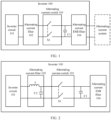
- FIG. 1 is a schematic block diagram of an inverter according to an exemplary embodiment, which is not part of the claims.
- An inverter 100 shown in FIG. 1 specifically includes: an inverter circuit 101, an alternating current filter 102, an alternating current switch 103, and an alternating current EMI filter 104.
- An output port of the inverter circuit 101 is connected to an input port of the alternating current filter 102, and the alternating current switch 103 is connected between an output port of the alternating current filter 102 and an input port of the alternating current EMI filter 104.
- the alternating current switch 103 may be specifically a first alternating current switch S1.
- the inverter 100 further includes a first split capacitor C1, and C1 is disposed between S1 and the input port of the alternating current EMI filter 104.
- C1 is disconnected from the output port of the alternating current filter 102, and C1 is connected to a circuit in which an alternating current system connected to the output port of the alternating current EMI filter 104 is located, to suppress harmonic distortion of the alternating current system.
- S1 is turned on, the first split capacitor is connected to the output port of the alternating current filter.
- the first split capacitor constitutes a filter capacitor of the alternating current filter.
- an output port of the inverter 100 may further be connected to the alternating current system.
- the inverter 100 may convert a direct current into an alternating current by using the inverter circuit 101, perform, by using the alternating current filter 102 and the alternating current EMI filter 104, filtering processing on the alternating current obtained through conversion by using the inverter circuit 101, and transmit an alternating current obtained after filtering processing to the alternating current system.
- the alternating current system may be used for power supply after obtaining the alternating current.
- C1 is a capacitor of the alternating current filter, but C1 is disposed outside the output port of the alternating current filter 102. When S1 is turned on, C1 actually constitutes the filter capacitor of the alternating current filter.
- C1 is all capacitors or some capacitors of the alternating current filter.
- the alternating current filter 102 may further include another capacitor, and the another capacitor may be located between the input port and the output port of the alternating current filter 102.
- the first split capacitor may be a single-phase capacitor or may be a three-phase capacitor.
- the first alternating current switch is a single-phase alternating current switch.
- the first alternating current switch is a three-phase alternating current switch, and the first split capacitor is constituted by three-phase branch capacitors.
- the first split capacitor may be constituted by a first branch capacitor, a second branch capacitor, and a third branch capacitor.
- the first split capacitor when the first alternating current switch is turned off, the first split capacitor is connected to the circuit in which the alternating current system is located, and can change a capacitance value of the circuit in which the alternating current system is located, so that the harmonic distortion of the alternating current system can be suppressed.
- the harmonic distortion of the alternating current system can be suppressed by disposing an original capacitor and an original switch of the alternating current filter, and no additional component is added. Therefore, no additional hardware costs or power consumption is caused.
- the resonance frequency of a resonant branch of the alternating current system is related to a capacitor and an inductor that are included in the resonant branch.
- the output port of the alternating current filter 102 is connected to the input port of the alternating current EMI filter 104 by using S 1
- C1 is connected in parallel to the input port of the alternating current EMI filter 104
- C1 is connected in parallel to the output port of the alternating current filter 102 by using S 1.
- the alternating current filter 102 includes an inductor L connected in series between the input port and the output port of the alternating current filter 102 and includes a second split capacitor C2, and C2 is connected in parallel between the input port and the output port of the alternating current filter 102 and disposed between the inductor L and the output port of the alternating current filter; and when S 1 is turned off, C2 constitutes the filter capacitor of the alternating current filter 102; or when S1 is turned on, C1 and C2 are connected in parallel and then connected in series to the inductor L, to jointly constitute the filter capacitor of the alternating current filter 102.
- the filter capacitor of the alternating current filter 102 is configured to filter an alternating current obtained through inversion by the inverter circuit 102.
- S 1 can be used to flexibly control whether the some filter capacitors of the alternating current filter are connected to the alternating current system or constitute the filter capacitor of the alternating current filter, and to flexibly control that the some capacitors of the alternating current filter are connected to the alternating current system when the harmonic distortion needs to be suppressed.
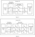
- the alternating current switch 103 may further include a second alternating current switch S2.
- the alternating current switch 103 in the inverter 100 further includes the second alternating current switch S2, S2 is disposed between S 1 and the input port of the alternating current EMI filter 104, and C1 is disposed between S1 and S2; and when S1 is turned off and S2 is turned on, C1 is disconnected from the output port of the alternating current filter 102, and C1 is connected to a circuit in which an alternating current system connected to the output port of the inverter 100 is located, to change a capacitance value of the circuit in which the alternating current system is located; or when S1 is turned on and S2 is turned off, C1 and C2 are connected in parallel and then connected in series to the inductor L of the filter, to jointly constitute the filter capacitor of the alternating current filter 102.
- C1 is connected to the circuit in which the alternating current system is located, so that the capacitance value of the resonant branch of the alternating current system can be changed, and the resonant frequency of the resonant branch of the alternating current system can be changed, thereby suppressing the harmonic distortion of the alternating current system.
- constitution of the filter capacitor of the alternating current filter can be more conveniently adjusted by using the two alternating current switches.
- the output port of the alternating current filter 102 is connected to the input port of the alternating current EMI filter 104 by using S 1 and S2, C1 is connected in parallel to the output port of the alternating current filter 102 by using S1, and C1 is connected in parallel to the input port of the alternating current EMI filter 104 by using S2.
- C1 and C2 each may be a single capacitor, or may be constituted by connecting a plurality of capacitors in parallel.
- the alternating current switch 103 may include only S 1, or may include both S 1 and S2.
- a specific structure of the alternating current switch 103 differs. With reference to FIG. 4 to FIG. 6 , the following describes in detail the specific structure of the alternating current switch 103 and a connection relationship among the alternating current switch 103, the alternating current filter 102, and the alternating current EMI filter 104.
- the alternating current switch 103 includes a single-phase alternating current switch S1.
- Fixed ends of S1 include A1, A2, B1, and B2, and movable ends of S1 include D1 and D2.
- C1 is a single-phase capacitor, and two ends of C1 are E1 and E2.
- D1 and D2 are respectively connected to the fixed ends A1 and A2.
- S1 is turned on.
- the fixed ends A1 and A2 are respectively connected to the fixed ends B 1 and B2, to implement conduction of S 1.
- the output port of the alternating current filter 102 is connected to the input port of the alternating current EMI filter 104.
- E1 and E2 are respectively connected to the fixed ends B1 and B2 of S1, and E1 and E2 are further directly connected to the input port of the alternating current EMI filter 104.
- the filter capacitor of the alternating current filter 102 includes a second split capacitor C2. Connection relationships between fixed ends and movable ends of S1 are the same as those in FIG. 4 .
- C1 and C2 each are a single-phase capacitor.
- C1 has two ends E1 and E2, and C2 has two ends E3 and E4.
- E1 and E2 are respectively connected to fixed ends B1 and B2 of S1, E1 and E2 are further directly connected to the input port of the alternating current EMI filter 104, and E3 and E4 are respectively connected to fixed ends A1 and A2 of S 1.
- the alternating current switch 103 includes single-phase alternating current switches S1 and S2, and S1 and S2 are disposed between the output port of the alternating current filter 102 and the input port of the alternating current EMI filter 104.
- C1 and C2 each are a single-phase capacitor, C1 is located between S1 and S2, and C2 is disposed between the input port and the output port of the alternating current filter 102.
- fixed ends of S1 include A1, A2, B1, and B2, movable ends of S1 include D1 and D2.
- Fixed ends of S2 include A3, A4, B3, and B4, and movable ends of S2 include D3 and D4.
- Two ends of C1 are E1 and E2, and two ends of C2 are E3 and E4.
- S1, D1 and D2 are respectively connected to A1 and A2.
- S2, D3 and D4 are respectively connected to A3 and A4.
- D3 and D4 are respectively connected to B3 and B4, S2 is turned on.
- C1 E1 and E2 are respectively connected to B1 and B2, E1 and E2 are respectively connected to A3 and A4, and E3 and E4 are respectively connected to the fixed ends A1 and A2 of S1.
- C1 may be alternatively disposed between S2 and the input port of the alternating current EMI filter 104, wherein this embodiment is not part of the claims.
- the alternating current switch 103 includes S1 and S2, and connection relationships between fixed ends and movable ends of S1 and S2 are the same as those in FIG. 6 .
- two ends E1 and E2 of C1 are respectively connected to movable ends B3 and B4 of S2, and E1 and E2 are further separately connected to the input port of the alternating current EMI filter 104.
- the inverter shown in FIG. 7 may further include C2, and a port included by C2 and a connection relationship between C2 and another port may be as shown in FIG. 6 .
- the alternating current switch 103 shown in FIG. 7 is the same as the alternating current switch 103 shown in FIG. 6 .
- a difference lies in that, in FIG. 6 , C1 is located between S1 and S2, but in FIG. 7 , C1 is located between S2 and the alternating current EMI filter 104.
- the filter capacitor in the alternating current filter 102 is the single-phase capacitor
- the alternating current switch included by the alternating current switch 103 is the single-phase alternating current switch.
- the filter capacitor in the alternating current filter 102 may alternatively be a three-phase capacitor
- the alternating current switch in the alternating current switch 103 may alternatively be a three-phase alternating current switch.
- FIG. 8 and FIG. 9 the following describes in detail a case in which the filter capacitor is the three-phase capacitor and the alternating current switch is the three-phase alternating current switch.
- the alternating current switch 103 includes a first alternating current switch S1, fixed ends of S1 include A1, A2, A3, B1, B2, and B3, and movable ends of S1 include D1, D2, and D3.
- the movable ends D1, D2, and D3 of S1 are respectively connected to the fixed ends B1, B2, and B3 of S1, S1 is turned on.
- the fixed ends A1, A2, and A3 are respectively connected to the fixed ends B1, B2, and B3, to implement conduction of S1.
- the output port of the alternating current filter 102 is connected to the input port of the alternating current EMI filter 104.
- C1 is a three-phase capacitor
- C1 is constituted by a first branch capacitor, a second branch capacitor, and a third branch capacitor.
- the first branch capacitor includes a first end E1 and a second end E2
- the second branch capacitor includes a third end E3 and a fourth end E4
- the third branch capacitor includes a fifth end E5 and a sixth end E6.
- E1, E3, and E5 are respectively connected to the fixed ends B1, B2, and B3, and E2, E4, and E6 are connected to each other.
- the alternating current switch 103 includes a first alternating current switch S1 and a second alternating current switch S2.
- Fixed ends of S1 include A1, A2, A3, B1, B2, and B3, and movable ends of S1 include D1, D2, and D3.
- Fixed ends of S1 include A1, A2, A3, B1, B2, and B3, and movable ends of S1 include D1, D2, and D3.
- Fixed ends of S2 include A4, A5, A6, B4, B5, and B6, and movable ends of S2 include D4, D5, and D6.
- C1 is a three-phase capacitor, and C1 is constituted by a first branch capacitor, a second branch capacitor, and a third branch capacitor.
- a first end to a sixth end of C1 are E1, E2, E3, E4, E5, and E6.
- E1, E3, and E5 are respectively connected to the fixed ends B1, B2, and B3.
- E1, E3, and E5 are further respectively connected to the fixed ends B4, B5, and B6.
- E2, E4, and E6 are connected to each other.
- a capacitance value of the first split capacitor is K times a capacitance value of the filter capacitor, where K is a value that enables the harmonic distortion of the alternating current system to be less than preset harmonic distortion.
- the value of K is an integer greater than 0 and less than or equal to 1, and the value of K may be obtained based on an actual test. Specifically, in the actual test, the value of K may be set, and a ratio of the first split capacitor to the filter capacitor when the harmonic distortion of the alternating current system meets a preset requirement is determined as the value of K.
- the value of K may be estimated based on an equivalent capacitor of the alternating current EMI filter, an equivalent inductor of the alternating current system, and a harmonic of the alternating current system.
- the capacitance value of the first split capacitor is C1
- the capacitance value of the filter capacitor is C
- C1 K x C.
- a frequency of a system harmonic of the alternating current system is 2 kHz.
- K 0.2
- a frequency band in which a minimum impedance of the alternating current system is located is also 2 kHz.
- K is greater than or equal to 0.2
- a frequency band in which a minimum impedance of the alternating current system is located is gradually away from a frequency band in which the system harmonic is located, thereby avoiding excessive amplification of the system harmonic. Therefore, when the value of K is set, the value of K may be set to a comparatively large value (for example, the value of K is set to a value close to 1) depending on a situation.
- a direct current system, and an alternating current system jointly constitute a grid-tied power generating system, to suppress the harmonic distortion of the alternating current system
- S1 may be kept turned off (in an initial state, S1 is turned off, and no operation needs to be performed on S1 at this time).
- C1 is disconnected from the alternating current filter 102, and is connected to an alternating current system in which the alternating current EMI filter 104 is located, so that the harmonic distortion of the alternating current system can be suppressed.
- a direct current system, and an alternating current system jointly constitute a grid-tied power generating system, to suppress the harmonic distortion of the alternating current system
- S1 may be kept turned off and S2 may be turned on (in an initial state, both S1 and S2 are turned off, and in this case, only S2 needs to be turned on).
- C1 is disconnected from the alternating current filter 102, and is connected to an alternating current system in which the alternating current EMI filter 104 is located, so that the harmonic distortion of the alternating current system can be suppressed.
- S2 may be kept turned off (in an initial state, both S 1 and S2 are turned off, and in this case, only S2 needs to be turned off, and S1 may be turned off or may be turned on).
- C1 is disconnected from the alternating current filter 102, and is connected to an alternating current system in which the alternating current EMI filter 104 is located, so that the harmonic distortion of the alternating current system can be suppressed.
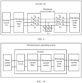
- the grid-tied power generating system includes a direct current system, an alternating current system, and an inverter.
- An output port of the direct current system is connected to an input port of the inverter, and an output port of the inverter is connected to an input port of the alternating current system.
- the direct current system is configured to output a direct current
- the inverter is configured to convert the direct current output by the direct current system into an alternating current
- the alternating current system is configured to provide the alternating current.
- the alternating current system in FIG. 10 may be specifically an alternating current system and is configured to provide the alternating current.
- the inverter shown in FIG. 10 may be any one of the inverters shown in any of FIG. 1 to FIG. 9 .
- a limitation and an explanation of the inverter in the embodiments of this application are also applicable to the inverter in the grid-tied power generating system shown in FIG. 10
- an alternating current switch in the grid-tied power generating system is set to be turned off, a first split capacitor may be disconnected from an alternating current filter, and the first split capacitor is connected to a circuit in which an alternating current system connected to the input port of the inverter is located, so that distortion of the alternating current system can be suppressed.
- the inverter in the grid-tied power generating system in this embodiment of this application may be a single-phase inverter or may be a three-phase inverter.
- a filter capacitor of the alternating current filter includes a first single-phase split capacitor C1 and a second single-phase split capacitor C2, and the alternating current switch includes a first single-phase alternating current switch S1 and a second single-phase alternating current switch S2.
- the second single-phase split capacitor C2 is connected in parallel to a single-phase filter inductor L.
- the parallel branch may be considered as a whole.
- a front end point of the parallel branch is connected to an alternating current side of an inverter circuit, and a back end point is sequentially connected in series to the first single-phase alternating current switch S1 of the alternating current switch.
- the first single-phase split capacitor C1 is connected in parallel to the first single-phase alternating current switch S1, the parallel branch may be considered as a whole, and the parallel branch is sequentially connected in series to the second single-phase alternating current switch S2 of the alternating current switch.
- the second single-phase alternating current switch S2 of the alternating current switch may be controlled to be turned on, to connect the first single-phase split capacitor C1 to the alternating current system, and dynamically change a resonance frequency of a resonant branch of the alternating current system, thereby staggering a frequency band in which a system harmonic voltage is located. This avoids excessive amplification of the system harmonic voltage and ensures that the single-phase inverter automatically starts.
- first single-phase split capacitor C1 shown in FIG. 11 may be equivalent to the foregoing first split capacitor, and the first single-phase split capacitor C1 may be some capacitors of the filter capacitors of the alternating current filter.
- a filter capacitor includes a first three-phase split capacitor C1 and a second three-phase split capacitor C2, and the alternating current switch includes a first three-phase alternating current switch S1 and a second three-phase alternating current switch S2.
- the second three-phase split capacitor C2 is connected in parallel to a three-phase filter inductor L.
- the parallel branch may be considered as a whole.
- a front end point of the parallel branch is connected to an alternating current side of an inverter circuit, and a back end point is sequentially connected in series to the first three-phase alternating current switch S1 of the alternating current switch.
- the first three-phase split capacitor C1 is connected in parallel to the first three-phase alternating current switch S1, the parallel branch may be considered as a whole, and the parallel branch is sequentially connected in series to the second three-phase alternating current switch S2 of the alternating current switch.
- the second three-phase alternating current switch S2 of the alternating current switch may be controlled to be turned on, to connect the first three-phase split capacitor C1 to the alternating current system, and dynamically change a resonance frequency of a resonant branch of the alternating current system, thereby staggering a frequency band in which a system harmonic voltage is located. This avoids excessive amplification of the system harmonic voltage and ensures that the three-phase inverter automatically starts.
- first three-phase split capacitor C1 shown in FIG. 12 may be equivalent to the foregoing first split capacitor, and the first three-phase split capacitor C1 may be some capacitors of the filter capacitors of the alternating current filter.
- the grid-tied power generating system may include one inverter or may include a plurality of inverters. It should be understood that, in the grid-tied power generating system, one direct current system corresponds to one inverter, and each inverter is configured to convert a direct current output by a corresponding direct current system into an alternating current. However, there may be only one alternating current system, and finally, alternating currents obtained through conversion by the plurality of inverters may be input into the alternating current system.
- This application further provides a grid-tied power generating system, where the grid-tied power generating system includes an alternating current system, N inverters according to the embodiments of this application, and N direct current systems, output ports of the N direct current systems are connected to input ports of the N inverters in a one-to-one manner, and N is an integer greater than or equal to 1, and output ports of the N inverters are connected to an input port of an alternating current system.
- a grid-tied power generating system includes N direct current systems (a direct current system 1 to a direct current system N, where N is an integer greater than or equal to 1) in total.
- the direct current system 1 to the direct current system N are respectively corresponding to an inverter 1 to an inverter N.
- the inverter 1 to the inverter N respectively convert direct currents input by the direct current system 1 to the direct current system N into alternating currents.
- the inverter 1 to the inverter N output the alternating currents obtained through conversion to an alternating current system.
- the alternating current system in this embodiment of the present invention is a power grid, for example, the State Grid.
- the direct current generated by the direct current system such as a photovoltaic solar panel or a wind turbine generator, is converted into an alternating current of a specific voltage and a specific working frequency by using the inverter, and then the alternating current is connected to the power grid.
- the grid-tied power generating system shown in FIG. 13 is a grid-tied power generating system constituted by N single-phase inverters, the N direct current systems, and the power grid.
- the grid-tied power generating system in this embodiment of this application may alternatively be constituted by N three-phase inverters, the N direct current systems, and the power grid.
- this application provides a method for suppressing the harmonic distortion of the power grid.
- some capacitors of filter capacitors of the inverter are connected to the power grid by operating an alternating current switch, thereby reducing the harmonic distortion of the power grid.
- An embodiment of this application further provides a photovoltaic power generating system.
- the photovoltaic power generating system includes a photovoltaic module, an alternating current power grid, and the inverter in the embodiments of this application.
- An output port of the photovoltaic module is connected to an input port of the inverter, and an output port of the inverter is configured to connect to an input port of the power grid.
- the photovoltaic module is configured to generate a direct current
- the inverter is configured to perform inversion processing on the direct current and input an alternating current obtained through the inversion processing into the power grid
- the power grid is configured to provide the alternating current.
- a first split capacitor can be connected, by controlling an alternating current switch in the inverter, to a circuit in which the power grid is located, so as to change a capacitance value of the circuit in which the power grid is located, to suppress harmonic distortion of the power grid.
- the photovoltaic module is a device that directly converts solar energy into electric energy by using a photovoltaic (photovoltaic) effect produced by a semiconductor material in a light condition.
- the photovoltaic module may also be referred to as a photovoltaic array or a solar panel.
- a rectifier may be further disposed in the photovoltaic power generating system.
- the rectifier is connected between the output port of the photovoltaic module and the input port of the inverter.
- the rectifier is configured to rectify the direct current generated by the photovoltaic module, and input a direct current obtained after rectification into the inverter.
- the photovoltaic power generating system in FIG. 14 is equivalent to a specific case of the grid-tied power generating system shown in any one of FIG. 10 to FIG. 13
- the photovoltaic module in the photovoltaic power generating system in FIG. 14 is equivalent to the direct current system in the grid-tied power generating system shown in any of FIG. 10 to FIG. 13 .
- the foregoing grid-tied power generating system may be a fan grid-tied power generating system or an energy storage grid-tied power generating system.
- the foregoing grid-tied power generating system may be specifically the fan grid-tied power generating system.
- the inverter in the embodiments of this application may be applied to the fan grid-tied power generating system.
- a rectifier may rectify an alternating current output by the fan grid-tied power generating system, to obtain a direct current.
- direct current voltage regulation is performed on the direct current by using a direct current capacitor.
- the inverter is configured to convert a direct current obtained through direct current voltage regulation into an alternating current, and transmit the alternating current to an alternating current power grid.
- a fan in FIG. 15 is equivalent to the direct current system in the grid-tied power generating system shown in any of FIG. 10 to FIG. 13 , and is configured to generate the direct current.
- the grid-tied power generating system may be specifically the energy storage grid-tied power generating system.
- the inverter in the embodiments of this application may be applied to the energy storage grid-tied power generating system, and the energy storage grid-tied power generating system is constituted by a storage system, the inverter, and an alternating current power grid.
- the inverter converts a direct current output by an energy storage system into an alternating current, and transmits the alternating current obtained through conversion to the alternating current power grid.
- the energy storage system in FIG. 16 is equivalent to the direct current system in the grid-tied power generating system shown in any of FIG. 10 to FIG. 13 , and is configured to generate the direct current.
- FIG. 17 is a schematic flowchart of a method for suppressing harmonic distortion according to an embodiment of this application.
- the method shown in FIG. 17 may be applied to a grid-tied power generating system.
- the grid-tied power generating system includes N inverters, a direct current system, and a power grid. Input ports of the N inverters are connected to an output port of the direct current system, and output ports of the N inverters are connected to an input port of the power grid.
- a specific structure of the inverter in the grid-tied power generating system may be as shown in FIG. 6 , FIG. 9 , or FIG. 12 .
- an alternating current switch of the inverter in the grid-tied power generating system to which the method shown in FIG.
- a first split capacitor is disposed between the first alternating current switch and the second alternating current switch.
- the second alternating current switch is turned on and the first alternating current switch is kept turned off, and the first split capacitor can be connected to a circuit in which the power grid is located.
- the grid-tied power generating system to which the method shown in FIG. 17 is applied may be as shown in FIG. 16 .
- the method shown in FIG. 17 specifically includes step 1001 and step 1002. The following separately describes step 1001 and step 1002 in detail.
- the second alternating current switch of the at least one of the N inverters is controlled to be turned on, so that a first split capacitor of the at least one inverter can be connected to a circuit in which a power grid connected to an output port of the inverter is located, and the first split capacitor is disconnected from an output port of an alternating current filter, so that harmonic distortion of the power grid can be suppressed. Therefore, the current THD can be reduced by turning on the second alternating current switch of the at least one of the N inverters.
- first split capacitors of some inverters can be connected to the power grid by controlling an alternating current switch of an inverter in the grid-tied power generating system to be turned on, so that the harmonic distortion of the power grid voltage of the power grid can be suppressed.
- the first split capacitor can be connected in parallel to the power grid by controlling the alternating current switch to be turned off or turned on.
- a resonance frequency of a resonant branch of the system can be dynamically changed, thereby staggering a frequency band in which a system harmonic voltage of the alternating current system is located, and avoiding excessive amplification of the system harmonic voltage.
- the controlling a second alternating current switch of at least one of the N inverters to be turned on, to enable the current THD to be less than the preset threshold includes: after a second alternating current switch of one of the N inverters is turned on, repeatedly performing step 1001 and step 1002 until the current THD is less than or equal to the preset threshold.
- the current THD is determined in time.
- the current THD is reduced by continuing to turn on a second alternating current switch of the inverter, to enable the current THD to be less than or equal to the preset threshold.
- the current THD can be gradually changed by turning on second alternating current switches of the inverters one by one, so that the current THD can finally be less than or equal to the preset threshold, thereby suppressing the harmonic distortion.
- the harmonic distortion can be flexibly suppressed by controlling the alternating current switch to be turned off or turned on.
- an alternating current switch that is not turned on in the inverter may be turned on, to constitute a complete circuit, so that the inverter can convert a direct current generated by the direct current system into an alternating current, and transmit the alternating current to the power grid.
- the direct current system may be a power generating system, for example, a wind power generating system or a photovoltaic power generating system.
- That the direct current system meets the power generating condition may mean that the power generating system can normally generate power.
- that the direct current system meets the power generation condition may mean that a wind power level reaches a preset requirement and a fan can normally generate power.
- the method for suppressing harmonic distortion in this embodiment of this application may be applied to a plurality of application scenarios.
- the method for suppressing harmonic distortion in this embodiment of this application may be applied to two scenarios: a grid-tied operation scenario and an off-grid shutdown scenario.
- the following describes in detail the method for suppressing harmonic distortion in this embodiment of this application in the two scenarios.
- FIG. 18 is a specific flowchart of the method for suppressing harmonic distortion in the grid-tied operation scenario according to an embodiment of this application.
- the method shown in FIG. 18 may be applied to the grid-tied power generating system shown in FIG. 16 .
- the method shown in FIG. 18 can be used for performing harmonic suppression on the grid-tied power generating system shown in FIG. 16 .
- the method shown in FIG. 18 specifically includes the following steps.
- a power grid voltage of a grid-tied point of each of the N inverters is collected and a THD analysis is made, to obtain current THD of the power grid voltage.
- THDm is a specified THD threshold that meets normal starting-up of the inverter. If the current THD is greater than THDm, step 2004 is performed. If the current THD is less than THDm, step 2005 is performed.
- step 2002 is performed again to make a THD analysis to obtain current THD, and then step 2003 is performed again. If the current THD is greater than THDm, step 2004 is performed again. If the current THD is less than THDm, step 2005 is performed.
- the inverter can start normally, so that the inverter in the system is connected to the power grid securely and stably.
- FIG. 19 is a specific flowchart of the method for suppressing harmonic distortion in the grid-tied operation scenario according to an embodiment of this application.
- the method shown in FIG. 19 may be applied to the grid-tied power generating system shown in FIG. 16 .
- the method shown in FIG. 19 can be used for performing harmonic suppression on the grid-tied power generating system shown in FIG. 16 .
- a specific procedure of the method shown in FIG. 19 includes the following steps.
- THDm is a specified THD threshold that meets normal starting-up of the inverter. If the current THD is greater than THDm, step 3004 is performed. If the current THD is less than THDm, step 3005 is performed.
- step 3002 is performed again to make a THD analysis to obtain current THD, and then step 3003 is performed again. If the current THD is greater than THDm, step 3004 is performed again. If the current THD is less than THDm, step 3005 is performed.
- the inverter is started normally to implement grid-tied operation.
- the current THD is less than THDm. This implements harmonic suppression on the power grid voltage when the inverter is in an off-grid shutdown state.
- the method shown in FIG. 18 finally needs to implement normal starting-up of the inverter, to implement normal operation of the grid-tied power generating system, and to suppress harmonic distortion of the power grid in a starting-up process or before starting-up.
- the method shown in FIG. 19 is merely intended to implement harmonic distortion suppression on the power grid when the inverter is in an off-grid shutdown state.
Landscapes
- Engineering & Computer Science (AREA)
- Power Engineering (AREA)
- Physics & Mathematics (AREA)
- Electromagnetism (AREA)
- Inverter Devices (AREA)
Claims (7)
- Wechselrichter (100), der Folgendes umfasst:eine Wechselrichterschaltung (101);ein Wechselstromfilter (102), wobei ein Eingangsanschluss des Wechselstromfilters mit einem Ausgangsanschluss der Wechselrichterschaltung verbunden ist;ein Wechselstrom-Elektromagnetische-Störung- bzw. Wechselstrom-EMI-Filter (104);einen ersten Wechselstromschalter (S1), der zwischen einem Ausgangsanschluss des Wechselstromfilters (102) und einem Eingangsanschluss des Wechselstrom-EMI-Filters (104) verbunden ist;wobei der Wechselrichter ferner einen ersten Teilungskondensator (C1) umfasst und der erste Teilungskondensator (C1) zwischen dem ersten Wechselstromschalter (S1) und dem Eingangsanschluss des Wechselstrom-EMI-Filters (104) angeordnet ist;wobei das Wechselstromfilter (102) eine Induktivität (L) umfasst, die zwischen dem Eingangsanschluss und dem Ausgangsanschluss des Wechselstromfilters (102) in Reihe geschaltet ist und einen zweiten Teilungskondensator (C2) umfasst, und der zweite Teilungskondensator (C2) zwischen dem Eingangsanschluss und dem Ausgangsanschluss des Wechselstromfilters (102) parallel geschaltet ist und zwischen der Induktivität L und dem Ausgangsanschluss des Wechselstromfilters (102) angeordnet ist,dadurch gekennzeichnet, dassder Wechselrichter ferner einen zweiten Wechselstromschalter (S2) umfasst, der zwischen dem ersten Wechselstromschalter (S1) und dem Eingangsanschluss des Wechselstrom-EMI-Filters (104) angeordnet ist, wobei der erste Teilungskondensator (C1) zwischen dem ersten Wechselstromschalter (S1) und dem zweiten Wechselstromschalter (S2) angeordnet ist,wobei der Wechselrichter derart ausgelegt ist, dasswenn der erste Wechselstromschalter (S1) ausgeschaltet ist und der zweite Wechselstromschalter (S2) eingeschaltet ist, der erste Teilungskondensator (C1) von dem Ausgangsanschluss des Wechselstromfilters (102) getrennt wird und der erste Teilungskondensator (C1) mit einer Schaltung verbunden wird, in der sich ein mit dem Ausgangsanschluss des Wechselrichters (100) verbundenes Wechselstromsystem befindet, sodass ein Kapazitätswert der Schaltung, in der sich das Wechselstromsystem befindet, erhöht wird, um eine in das Wechselstromsystem eingegebene Oberschwingungsverzerrung zu unterdrücken, undwobei der Wechselrichter derart ausgelegt ist, dasswenn der erste Wechselstromschalter (S1) eingeschaltet ist und der zweite Wechselstromschalter (S2) ausgeschaltet ist, der erste Teilungskondensator (C1) und der zweite Teilungskondensator (C2) parallel geschaltet sind und dann mit der Induktivität L des Filters in Reihe geschaltet sind, um gemeinsam den Filterkondensator des Wechselstromfilters (102) zu bilden.
- Wechselrichter nach Anspruch 1, wobei der Ausgangsanschluss des Wechselstromfilters (102) unter Verwendung des ersten Wechselstromschalters (S1) und des zweiten Wechselstromschalters (S2) mit dem Eingangsanschluss des Wechselstrom-EMI-Filters (104) verbunden ist, der erste Teilungskondensator (C1) mittels des ersten Wechselstromschalters (S1) mit dem Ausgangsanschluss des Wechselstromfilters (102) parallel geschaltet ist und der erste Teilungskondensator (C1) mittels des zweiten Wechselstromschalters (S2) mit dem Eingangsanschluss des Wechselstrom-EMI-Filters (104) parallel geschaltet ist.
- Fotovoltaisches Stromerzeugungssystem, wobei das System ein Fotovoltaikmodul und den Wechselrichter (100) nach Anspruch 1 oder 2 umfasst, ein Ausgangsanschluss des Fotovoltaikmoduls mit einem Eingangsanschluss des Wechselrichters (100) verbunden ist, ein Ausgangsanschluss des Wechselrichters (100) ausgelegt ist zum Verbinden mit einem Eingangsanschluss eines Wechselstromsystems, das Fotovoltaikmodul ausgelegt ist zum Erzeugen eines Gleichstroms und der Wechselrichter ausgelegt ist zum Durchführen einer Inversionsverarbeitung an dem Gleichstrom und Eingeben eines durch Inversionsverarbeitung erhaltenen Wechselstroms in das Wechselstromsystem.
- Netzgebundenes Stromerzeugungssystem, wobei das System N Wechselrichter (100) nach Anspruch 1 und N Gleichstromsysteme umfasst, Ausgangsanschlüsse der N Gleichstromsysteme eineindeutig mit Eingangsanschlüssen der N Wechselrichter (100) verbunden sind und N eine ganze Zahl größer oder gleich 1 ist und Ausgangsanschlüsse der N Wechselrichter mit einem Eingangsanschluss eines Wechselstromsystems verbunden sind.
- Verfahren zum Unterdrückten von Oberschwingungsverzerrung eines netzgebundenen Stromerzeugungssystems nach Anspruch 4, und wenn sowohl ein erster Wechselstromschalter (S1) als auch ein zweiter Wechselstromschalter (S2) in beliebigen der N Wechselrichter (100) ausgeschaltet werden, umfasst das Verfahren Folgendes:Schritt 1: Erhalten einer aktuellen Oberschwingungsgesamtverzerrung THD einer Spannung des Wechselstromsystems; undSchritt 2: wenn die aktuelle THD größer als eine voreingestellte Schwelle ist, dahingehendes Steuern eines zweiten Wechselstromschalters (S2) mindestens eines der N Wechselrichter (100), eingeschaltet zu werden, um zu ermöglichen, dass die aktuelle THD kleiner als die voreingestellte Schwelle ist.
- Verfahren nach Anspruch 5, wobei das dahingehende Steuern eines zweiten Wechselstromschalters (S2) mindestens eines der N Wechselrichter (100), eingeschaltet zu werden, um zu ermöglichen, dass die aktuelle THD kleiner als die voreingestellte Schwelle ist, Folgendes umfasst:
nachdem ein zweiter Wechselstromschalter (S2) eines der N Wechselrichter (100) eingeschaltet wird, wiederholtes Durchführen von Schritt 1 und Schritt 2, bis die aktuelle THD kleiner oder gleich der voreingestellten Schwelle ist. - Verfahren nach Anspruch 6, wobei das Verfahren ferner Folgendes umfasst:wenn die aktuelle THD kleiner oder gleich der voreingestellten Schwelle ist, Bestimmen, ob eine Ausgangsspannung des Wechselrichters (100) eine Bedingung für netzgebundene Stromerzeugung erfüllt, undwenn die Ausgangsspannung des Wechselrichters (100) die Bedingung für netzgebundene Stromerzeugung erfüllt, Einschalten eines ersten Wechselstromschalters (S1) und eines zweiten Wechselstromschalters (S2), bei denen es sich um verbleibende nicht eingeschaltete Wechselstromschalter in den N Wechselrichtern (100) handelt.
Applications Claiming Priority (2)
| Application Number | Priority Date | Filing Date | Title |
|---|---|---|---|
| CN201810401979.1A CN110417016B (zh) | 2018-04-28 | 2018-04-28 | 逆变器、发电系统以及抑制交流系统谐波失真的方法 |
| PCT/CN2019/084623 WO2019206289A1 (zh) | 2018-04-28 | 2019-04-26 | 逆变器、发电系统以及抑制交流系统谐波失真的方法 |
Publications (3)
| Publication Number | Publication Date |
|---|---|
| EP3780308A1 EP3780308A1 (de) | 2021-02-17 |
| EP3780308A4 EP3780308A4 (de) | 2021-04-28 |
| EP3780308B1 true EP3780308B1 (de) | 2024-07-31 |
Family
ID=68293470
Family Applications (1)
| Application Number | Title | Priority Date | Filing Date |
|---|---|---|---|
| EP19792515.9A Active EP3780308B1 (de) | 2018-04-28 | 2019-04-26 | Wechselrichter, stromerzeugungssystem und verfahren zur unterdrückung der verzerrung von oberwellen |
Country Status (4)
| Country | Link |
|---|---|
| US (1) | US11336094B2 (de) |
| EP (1) | EP3780308B1 (de) |
| CN (1) | CN110417016B (de) |
| WO (1) | WO2019206289A1 (de) |
Families Citing this family (4)
| Publication number | Priority date | Publication date | Assignee | Title |
|---|---|---|---|---|
| WO2019012588A1 (ja) * | 2017-07-10 | 2019-01-17 | 東芝三菱電機産業システム株式会社 | パワーコンディショナ、電力システムおよび電力システムの無効電力抑制方法 |
| CN113890317B (zh) * | 2020-07-01 | 2025-06-17 | 株洲中车时代电气股份有限公司 | 一种无电压传感器的逆变器输出电压谐波抑制方法、逆变器多次谐波抑制控制器及应用方法 |
| CN112039337A (zh) * | 2020-09-02 | 2020-12-04 | 重庆中车四方所科技有限公司 | 一种空调应急通风电源电路系统 |
| CN119944818B (zh) * | 2025-04-07 | 2025-09-23 | 深圳鹏城新能科技有限公司 | 一种逆变器并网控制电路及控制方法 |
Family Cites Families (14)
| Publication number | Priority date | Publication date | Assignee | Title |
|---|---|---|---|---|
| JP2001268913A (ja) * | 2000-03-17 | 2001-09-28 | Daikin Ind Ltd | 三相整流装置 |
| CN100359779C (zh) * | 2006-05-08 | 2008-01-02 | 浙江大学 | 采用滤波器中间电流反馈的并网逆变器电流控制方法 |
| CN101494385A (zh) * | 2009-02-18 | 2009-07-29 | 常州瑞闪新能源有限公司 | 基于lcl滤波的太阳能光伏并网逆变器控制系统 |
| CN202014096U (zh) * | 2011-04-11 | 2011-10-19 | 河南天创风电设备有限公司 | 一种光伏并网逆变器的吸收和补偿装置 |
| CN102263417B (zh) | 2011-06-22 | 2013-07-10 | 清华大学 | 光伏并网用逆变器中lcl滤波器混合阻尼参数设计方法 |
| CN102522879B (zh) | 2011-11-18 | 2014-01-08 | 东南大学 | 一种lcl并网逆变器系统的有源阻尼方法及其电路 |
| CN103138544A (zh) * | 2011-11-29 | 2013-06-05 | 永济新时速电机电器有限责任公司 | 逆变器的输出滤波装置及电源转换装置 |
| CN102904286B (zh) * | 2012-10-23 | 2014-10-29 | 深圳市长昊机电有限公司 | 一种并网逆变器及其控制方法 |
| CN102969877B (zh) | 2012-11-16 | 2014-12-10 | 上海交通大学 | 采用分裂电容串联阻尼电阻的lcl滤波器设计方法 |
| CN103516248B (zh) * | 2013-09-26 | 2016-01-13 | 武汉大学 | 基于单电流环控制的llcl滤波并网逆变器 |
| CN103595063B (zh) * | 2013-11-21 | 2016-03-30 | 国网上海市电力公司 | 一种储能变流器及其电池储能系统 |
| JP6438117B2 (ja) * | 2014-09-30 | 2018-12-12 | ▲陽▼光▲電▼源股▲分▼有限公司Sungrow Power Supply Co., Ltd. | グリッドタイインバータ安全検出装置及び方法 |
| CN104836469A (zh) * | 2015-04-30 | 2015-08-12 | 祥天控股(集团)有限公司 | 并离网逆变电路 |
| CN104901568B (zh) * | 2015-06-25 | 2018-04-17 | 深圳市英威腾光伏科技有限公司 | 光伏逆变系统、光伏逆变器及其谐振抑制方法和装置 |
-
2018
- 2018-04-28 CN CN201810401979.1A patent/CN110417016B/zh active Active
-
2019
- 2019-04-26 EP EP19792515.9A patent/EP3780308B1/de active Active
- 2019-04-26 WO PCT/CN2019/084623 patent/WO2019206289A1/zh not_active Ceased
-
2020
- 2020-10-27 US US17/081,076 patent/US11336094B2/en active Active
Also Published As
| Publication number | Publication date |
|---|---|
| WO2019206289A1 (zh) | 2019-10-31 |
| CN110417016B (zh) | 2023-06-06 |
| EP3780308A4 (de) | 2021-04-28 |
| EP3780308A1 (de) | 2021-02-17 |
| US11336094B2 (en) | 2022-05-17 |
| CN110417016A (zh) | 2019-11-05 |
| US20210044110A1 (en) | 2021-02-11 |
Similar Documents
| Publication | Publication Date | Title |
|---|---|---|
| US11336094B2 (en) | Inverter, power generating system, and method for suppressing harmonic distortion of alternating current system | |
| Dursun et al. | LCL filter design for grid connected three-phase inverter | |
| US11088655B2 (en) | Photovoltaic solid-state transformer, photovoltaic inverter system and bidirectional high-voltage converter | |
| AU2020346195B2 (en) | Method, apparatus, and system for controlling string inverter, and storage medium | |
| US10727673B2 (en) | Transformerless power conversion | |
| US10951110B2 (en) | Control method and device for alternating-current and direct-current conversion circuit, and computer storage medium | |
| US9923481B2 (en) | Photovoltaic system and method for controlling the same | |
| Rahimi et al. | Optimal placement of additional switch in the photovoltaic single-phase grid-connected transformerless full bridge inverter for reducing common mode leakage current | |
| US20240136948A1 (en) | Grid-tied inverter apparatus and grid-tied control method | |
| CN104065285A (zh) | 并网逆变系统 | |
| EP4037171A1 (de) | Photovoltaischer solarwechselrichter mit netzfilter ohne induktivität | |
| CN106451497B (zh) | 一种孤岛模式下逆变器并联系统的谐振抑制方法 | |
| US12413159B2 (en) | Micro inverter and modulation method thereof | |
| US10998733B2 (en) | Power conversion system and associated control method | |
| CN201966825U (zh) | 并网寄生逆变器 | |
| CN116317658A (zh) | 一种应用母线电容串联方式的光伏逆变器 | |
| de Oliveira et al. | Operation of a high gain bidirectional DC-DC converter for photovoltaic on-grid systems | |
| CN220139435U (zh) | 一种微型逆变器 | |
| Wang et al. | CUK-SEPIC DC-DC CONVERTER INTEGRATED THREE-PHASE GRID-CONNECTED TRANSFORMERLESS INVERTER FOR PHOTOVOLTAIC APPLICATIONS | |
| CN104979822A (zh) | 智能微电网电力质量管理的操作系统 | |
| CN220964393U (zh) | 供电电路、电路板组件及电子设备 | |
| JP7666093B2 (ja) | 電力変換装置 | |
| CN212183417U (zh) | 一种大功率中频电源 | |
| Do et al. | Single-Phase 4-Switch Current-Fed Inverter With Eliminate Leakage Current: Published online: 03/11/2025 | |
| Chowdhury et al. | Design of a Compact 600VA Sinusoidal Inverter with Battery Storage System |
Legal Events
| Date | Code | Title | Description |
|---|---|---|---|
| STAA | Information on the status of an ep patent application or granted ep patent |
Free format text: STATUS: THE INTERNATIONAL PUBLICATION HAS BEEN MADE |
|
| PUAI | Public reference made under article 153(3) epc to a published international application that has entered the european phase |
Free format text: ORIGINAL CODE: 0009012 |
|
| STAA | Information on the status of an ep patent application or granted ep patent |
Free format text: STATUS: REQUEST FOR EXAMINATION WAS MADE |
|
| 17P | Request for examination filed |
Effective date: 20201109 |
|
| AK | Designated contracting states |
Kind code of ref document: A1 Designated state(s): AL AT BE BG CH CY CZ DE DK EE ES FI FR GB GR HR HU IE IS IT LI LT LU LV MC MK MT NL NO PL PT RO RS SE SI SK SM TR |
|
| AX | Request for extension of the european patent |
Extension state: BA ME |
|
| A4 | Supplementary search report drawn up and despatched |
Effective date: 20210325 |
|
| RIC1 | Information provided on ipc code assigned before grant |
Ipc: H02J 3/01 20060101AFI20210319BHEP Ipc: H02J 3/38 20060101ALI20210319BHEP Ipc: H02M 1/12 20060101ALI20210319BHEP |
|
| DAV | Request for validation of the european patent (deleted) | ||
| DAX | Request for extension of the european patent (deleted) | ||
| REG | Reference to a national code |
Ref country code: DE Free format text: PREVIOUS MAIN CLASS: H02J0003000000 Ipc: H02J0003010000 Ref country code: DE Ref legal event code: R079 Ref document number: 602019056180 Country of ref document: DE Free format text: PREVIOUS MAIN CLASS: H02J0003000000 Ipc: H02J0003010000 |
|
| RIC1 | Information provided on ipc code assigned before grant |
Ipc: H02M 1/12 20060101ALI20240118BHEP Ipc: H02J 3/38 20060101ALI20240118BHEP Ipc: H02J 3/01 20060101AFI20240118BHEP |
|
| GRAP | Despatch of communication of intention to grant a patent |
Free format text: ORIGINAL CODE: EPIDOSNIGR1 |
|
| STAA | Information on the status of an ep patent application or granted ep patent |
Free format text: STATUS: GRANT OF PATENT IS INTENDED |
|
| INTG | Intention to grant announced |
Effective date: 20240311 |
|
| GRAS | Grant fee paid |
Free format text: ORIGINAL CODE: EPIDOSNIGR3 |
|
| GRAA | (expected) grant |
Free format text: ORIGINAL CODE: 0009210 |
|
| STAA | Information on the status of an ep patent application or granted ep patent |
Free format text: STATUS: THE PATENT HAS BEEN GRANTED |
|
| AK | Designated contracting states |
Kind code of ref document: B1 Designated state(s): AL AT BE BG CH CY CZ DE DK EE ES FI FR GB GR HR HU IE IS IT LI LT LU LV MC MK MT NL NO PL PT RO RS SE SI SK SM TR |
|
| REG | Reference to a national code |
Ref country code: CH Ref legal event code: EP Ref country code: GB Ref legal event code: FG4D |
|
| REG | Reference to a national code |
Ref country code: DE Ref legal event code: R096 Ref document number: 602019056180 Country of ref document: DE |
|
| REG | Reference to a national code |
Ref country code: IE Ref legal event code: FG4D |
|
| REG | Reference to a national code |
Ref country code: LT Ref legal event code: MG9D |
|
| REG | Reference to a national code |
Ref country code: NL Ref legal event code: MP Effective date: 20240731 |
|
| PG25 | Lapsed in a contracting state [announced via postgrant information from national office to epo] |
Ref country code: PT Free format text: LAPSE BECAUSE OF FAILURE TO SUBMIT A TRANSLATION OF THE DESCRIPTION OR TO PAY THE FEE WITHIN THE PRESCRIBED TIME-LIMIT Effective date: 20241202 |
|
| REG | Reference to a national code |
Ref country code: AT Ref legal event code: MK05 Ref document number: 1709405 Country of ref document: AT Kind code of ref document: T Effective date: 20240731 |
|
| PG25 | Lapsed in a contracting state [announced via postgrant information from national office to epo] |
Ref country code: PT Free format text: LAPSE BECAUSE OF FAILURE TO SUBMIT A TRANSLATION OF THE DESCRIPTION OR TO PAY THE FEE WITHIN THE PRESCRIBED TIME-LIMIT Effective date: 20241202 |
|
| PG25 | Lapsed in a contracting state [announced via postgrant information from national office to epo] |
Ref country code: NO Free format text: LAPSE BECAUSE OF FAILURE TO SUBMIT A TRANSLATION OF THE DESCRIPTION OR TO PAY THE FEE WITHIN THE PRESCRIBED TIME-LIMIT Effective date: 20241031 |
|
| PG25 | Lapsed in a contracting state [announced via postgrant information from national office to epo] |
Ref country code: NL Free format text: LAPSE BECAUSE OF FAILURE TO SUBMIT A TRANSLATION OF THE DESCRIPTION OR TO PAY THE FEE WITHIN THE PRESCRIBED TIME-LIMIT Effective date: 20240731 Ref country code: FI Free format text: LAPSE BECAUSE OF FAILURE TO SUBMIT A TRANSLATION OF THE DESCRIPTION OR TO PAY THE FEE WITHIN THE PRESCRIBED TIME-LIMIT Effective date: 20240731 Ref country code: PL Free format text: LAPSE BECAUSE OF FAILURE TO SUBMIT A TRANSLATION OF THE DESCRIPTION OR TO PAY THE FEE WITHIN THE PRESCRIBED TIME-LIMIT Effective date: 20240731 Ref country code: GR Free format text: LAPSE BECAUSE OF FAILURE TO SUBMIT A TRANSLATION OF THE DESCRIPTION OR TO PAY THE FEE WITHIN THE PRESCRIBED TIME-LIMIT Effective date: 20241101 |
|
| PG25 | Lapsed in a contracting state [announced via postgrant information from national office to epo] |
Ref country code: BG Free format text: LAPSE BECAUSE OF FAILURE TO SUBMIT A TRANSLATION OF THE DESCRIPTION OR TO PAY THE FEE WITHIN THE PRESCRIBED TIME-LIMIT Effective date: 20240731 |
|
| PG25 | Lapsed in a contracting state [announced via postgrant information from national office to epo] |
Ref country code: LV Free format text: LAPSE BECAUSE OF FAILURE TO SUBMIT A TRANSLATION OF THE DESCRIPTION OR TO PAY THE FEE WITHIN THE PRESCRIBED TIME-LIMIT Effective date: 20240731 |
|
| PG25 | Lapsed in a contracting state [announced via postgrant information from national office to epo] |
Ref country code: AT Free format text: LAPSE BECAUSE OF FAILURE TO SUBMIT A TRANSLATION OF THE DESCRIPTION OR TO PAY THE FEE WITHIN THE PRESCRIBED TIME-LIMIT Effective date: 20240731 Ref country code: IS Free format text: LAPSE BECAUSE OF FAILURE TO SUBMIT A TRANSLATION OF THE DESCRIPTION OR TO PAY THE FEE WITHIN THE PRESCRIBED TIME-LIMIT Effective date: 20241130 |
|
| PG25 | Lapsed in a contracting state [announced via postgrant information from national office to epo] |
Ref country code: HR Free format text: LAPSE BECAUSE OF FAILURE TO SUBMIT A TRANSLATION OF THE DESCRIPTION OR TO PAY THE FEE WITHIN THE PRESCRIBED TIME-LIMIT Effective date: 20240731 |
|
| PG25 | Lapsed in a contracting state [announced via postgrant information from national office to epo] |
Ref country code: RS Free format text: LAPSE BECAUSE OF FAILURE TO SUBMIT A TRANSLATION OF THE DESCRIPTION OR TO PAY THE FEE WITHIN THE PRESCRIBED TIME-LIMIT Effective date: 20241031 Ref country code: ES Free format text: LAPSE BECAUSE OF FAILURE TO SUBMIT A TRANSLATION OF THE DESCRIPTION OR TO PAY THE FEE WITHIN THE PRESCRIBED TIME-LIMIT Effective date: 20240731 |
|
| PG25 | Lapsed in a contracting state [announced via postgrant information from national office to epo] |
Ref country code: RS Free format text: LAPSE BECAUSE OF FAILURE TO SUBMIT A TRANSLATION OF THE DESCRIPTION OR TO PAY THE FEE WITHIN THE PRESCRIBED TIME-LIMIT Effective date: 20241031 Ref country code: PL Free format text: LAPSE BECAUSE OF FAILURE TO SUBMIT A TRANSLATION OF THE DESCRIPTION OR TO PAY THE FEE WITHIN THE PRESCRIBED TIME-LIMIT Effective date: 20240731 Ref country code: NO Free format text: LAPSE BECAUSE OF FAILURE TO SUBMIT A TRANSLATION OF THE DESCRIPTION OR TO PAY THE FEE WITHIN THE PRESCRIBED TIME-LIMIT Effective date: 20241031 Ref country code: NL Free format text: LAPSE BECAUSE OF FAILURE TO SUBMIT A TRANSLATION OF THE DESCRIPTION OR TO PAY THE FEE WITHIN THE PRESCRIBED TIME-LIMIT Effective date: 20240731 Ref country code: LV Free format text: LAPSE BECAUSE OF FAILURE TO SUBMIT A TRANSLATION OF THE DESCRIPTION OR TO PAY THE FEE WITHIN THE PRESCRIBED TIME-LIMIT Effective date: 20240731 Ref country code: IS Free format text: LAPSE BECAUSE OF FAILURE TO SUBMIT A TRANSLATION OF THE DESCRIPTION OR TO PAY THE FEE WITHIN THE PRESCRIBED TIME-LIMIT Effective date: 20241130 Ref country code: HR Free format text: LAPSE BECAUSE OF FAILURE TO SUBMIT A TRANSLATION OF THE DESCRIPTION OR TO PAY THE FEE WITHIN THE PRESCRIBED TIME-LIMIT Effective date: 20240731 Ref country code: GR Free format text: LAPSE BECAUSE OF FAILURE TO SUBMIT A TRANSLATION OF THE DESCRIPTION OR TO PAY THE FEE WITHIN THE PRESCRIBED TIME-LIMIT Effective date: 20241101 Ref country code: FI Free format text: LAPSE BECAUSE OF FAILURE TO SUBMIT A TRANSLATION OF THE DESCRIPTION OR TO PAY THE FEE WITHIN THE PRESCRIBED TIME-LIMIT Effective date: 20240731 Ref country code: ES Free format text: LAPSE BECAUSE OF FAILURE TO SUBMIT A TRANSLATION OF THE DESCRIPTION OR TO PAY THE FEE WITHIN THE PRESCRIBED TIME-LIMIT Effective date: 20240731 Ref country code: BG Free format text: LAPSE BECAUSE OF FAILURE TO SUBMIT A TRANSLATION OF THE DESCRIPTION OR TO PAY THE FEE WITHIN THE PRESCRIBED TIME-LIMIT Effective date: 20240731 Ref country code: AT Free format text: LAPSE BECAUSE OF FAILURE TO SUBMIT A TRANSLATION OF THE DESCRIPTION OR TO PAY THE FEE WITHIN THE PRESCRIBED TIME-LIMIT Effective date: 20240731 |
|
| PG25 | Lapsed in a contracting state [announced via postgrant information from national office to epo] |
Ref country code: RO Free format text: LAPSE BECAUSE OF FAILURE TO SUBMIT A TRANSLATION OF THE DESCRIPTION OR TO PAY THE FEE WITHIN THE PRESCRIBED TIME-LIMIT Effective date: 20240731 Ref country code: SM Free format text: LAPSE BECAUSE OF FAILURE TO SUBMIT A TRANSLATION OF THE DESCRIPTION OR TO PAY THE FEE WITHIN THE PRESCRIBED TIME-LIMIT Effective date: 20240731 Ref country code: DK Free format text: LAPSE BECAUSE OF FAILURE TO SUBMIT A TRANSLATION OF THE DESCRIPTION OR TO PAY THE FEE WITHIN THE PRESCRIBED TIME-LIMIT Effective date: 20240731 |
|
| PG25 | Lapsed in a contracting state [announced via postgrant information from national office to epo] |
Ref country code: EE Free format text: LAPSE BECAUSE OF FAILURE TO SUBMIT A TRANSLATION OF THE DESCRIPTION OR TO PAY THE FEE WITHIN THE PRESCRIBED TIME-LIMIT Effective date: 20240731 |
|
| PG25 | Lapsed in a contracting state [announced via postgrant information from national office to epo] |
Ref country code: CZ Free format text: LAPSE BECAUSE OF FAILURE TO SUBMIT A TRANSLATION OF THE DESCRIPTION OR TO PAY THE FEE WITHIN THE PRESCRIBED TIME-LIMIT Effective date: 20240731 |
|
| PG25 | Lapsed in a contracting state [announced via postgrant information from national office to epo] |
Ref country code: IT Free format text: LAPSE BECAUSE OF FAILURE TO SUBMIT A TRANSLATION OF THE DESCRIPTION OR TO PAY THE FEE WITHIN THE PRESCRIBED TIME-LIMIT Effective date: 20240731 Ref country code: SK Free format text: LAPSE BECAUSE OF FAILURE TO SUBMIT A TRANSLATION OF THE DESCRIPTION OR TO PAY THE FEE WITHIN THE PRESCRIBED TIME-LIMIT Effective date: 20240731 |
|
| REG | Reference to a national code |
Ref country code: DE Ref legal event code: R097 Ref document number: 602019056180 Country of ref document: DE |
|
| PLBE | No opposition filed within time limit |
Free format text: ORIGINAL CODE: 0009261 |
|
| STAA | Information on the status of an ep patent application or granted ep patent |
Free format text: STATUS: NO OPPOSITION FILED WITHIN TIME LIMIT |
|
| 26N | No opposition filed |
Effective date: 20250501 |
|
| PGFP | Annual fee paid to national office [announced via postgrant information from national office to epo] |
Ref country code: DE Payment date: 20250305 Year of fee payment: 7 |
|
| PG25 | Lapsed in a contracting state [announced via postgrant information from national office to epo] |
Ref country code: SE Free format text: LAPSE BECAUSE OF FAILURE TO SUBMIT A TRANSLATION OF THE DESCRIPTION OR TO PAY THE FEE WITHIN THE PRESCRIBED TIME-LIMIT Effective date: 20240731 |
|
| REG | Reference to a national code |
Ref country code: CH Ref legal event code: H13 Free format text: ST27 STATUS EVENT CODE: U-0-0-H10-H13 (AS PROVIDED BY THE NATIONAL OFFICE) Effective date: 20251125 |
|
| PG25 | Lapsed in a contracting state [announced via postgrant information from national office to epo] |
Ref country code: LU Free format text: LAPSE BECAUSE OF NON-PAYMENT OF DUE FEES Effective date: 20250426 |
|
| PG25 | Lapsed in a contracting state [announced via postgrant information from national office to epo] |
Ref country code: MC Free format text: LAPSE BECAUSE OF FAILURE TO SUBMIT A TRANSLATION OF THE DESCRIPTION OR TO PAY THE FEE WITHIN THE PRESCRIBED TIME-LIMIT Effective date: 20240731 |
|
| GBPC | Gb: european patent ceased through non-payment of renewal fee |
Effective date: 20250426 |
|
| REG | Reference to a national code |
Ref country code: BE Ref legal event code: MM Effective date: 20250430 |
|
| PG25 | Lapsed in a contracting state [announced via postgrant information from national office to epo] |
Ref country code: GB Free format text: LAPSE BECAUSE OF NON-PAYMENT OF DUE FEES Effective date: 20250426 |
|
| PG25 | Lapsed in a contracting state [announced via postgrant information from national office to epo] |
Ref country code: FR Free format text: LAPSE BECAUSE OF NON-PAYMENT OF DUE FEES Effective date: 20250430 |
|
| PG25 | Lapsed in a contracting state [announced via postgrant information from national office to epo] |
Ref country code: BE Free format text: LAPSE BECAUSE OF NON-PAYMENT OF DUE FEES Effective date: 20250430 |
|
| PG25 | Lapsed in a contracting state [announced via postgrant information from national office to epo] |
Ref country code: CH Free format text: LAPSE BECAUSE OF NON-PAYMENT OF DUE FEES Effective date: 20250430 |
|
| PG25 | Lapsed in a contracting state [announced via postgrant information from national office to epo] |
Ref country code: IE Free format text: LAPSE BECAUSE OF NON-PAYMENT OF DUE FEES Effective date: 20250426 |