EP3780275B1 - Antennas-in-package verification board - Google Patents
Antennas-in-package verification board Download PDFInfo
- Publication number
- EP3780275B1 EP3780275B1 EP20191138.5A EP20191138A EP3780275B1 EP 3780275 B1 EP3780275 B1 EP 3780275B1 EP 20191138 A EP20191138 A EP 20191138A EP 3780275 B1 EP3780275 B1 EP 3780275B1
- Authority
- EP
- European Patent Office
- Prior art keywords
- board
- aip
- verification
- connectors
- antenna array
- Prior art date
- Legal status (The legal status is an assumption and is not a legal conclusion. Google has not performed a legal analysis and makes no representation as to the accuracy of the status listed.)
- Active
Links
Images



Classifications
-
- H—ELECTRICITY
- H01—ELECTRIC ELEMENTS
- H01P—WAVEGUIDES; RESONATORS, LINES, OR OTHER DEVICES OF THE WAVEGUIDE TYPE
- H01P5/00—Coupling devices of the waveguide type
- H01P5/02—Coupling devices of the waveguide type with invariable factor of coupling
- H01P5/022—Transitions between lines of the same kind and shape, but with different dimensions
- H01P5/028—Transitions between lines of the same kind and shape, but with different dimensions between strip lines
-
- H—ELECTRICITY
- H01—ELECTRIC ELEMENTS
- H01Q—ANTENNAS, i.e. RADIO AERIALS
- H01Q19/00—Combinations of primary active antenna elements and units with secondary devices, e.g. with quasi-optical devices, for giving the antenna a desired directional characteristic
- H01Q19/10—Combinations of primary active antenna elements and units with secondary devices, e.g. with quasi-optical devices, for giving the antenna a desired directional characteristic using reflecting surfaces
- H01Q19/104—Combinations of primary active antenna elements and units with secondary devices, e.g. with quasi-optical devices, for giving the antenna a desired directional characteristic using reflecting surfaces using a substantially flat reflector for deflecting the radiated beam, e.g. periscopic antennas
-
- G—PHYSICS
- G01—MEASURING; TESTING
- G01R—MEASURING ELECTRIC VARIABLES; MEASURING MAGNETIC VARIABLES
- G01R29/00—Arrangements for measuring or indicating electric quantities not covered by groups G01R19/00 - G01R27/00
- G01R29/08—Measuring electromagnetic field characteristics
- G01R29/10—Radiation diagrams of antennas
-
- G—PHYSICS
- G01—MEASURING; TESTING
- G01R—MEASURING ELECTRIC VARIABLES; MEASURING MAGNETIC VARIABLES
- G01R31/00—Arrangements for testing electric properties; Arrangements for locating electric faults; Arrangements for electrical testing characterised by what is being tested not provided for elsewhere
- G01R31/28—Testing of electronic circuits, e.g. by signal tracer
- G01R31/282—Testing of electronic circuits specially adapted for particular applications not provided for elsewhere
- G01R31/2822—Testing of electronic circuits specially adapted for particular applications not provided for elsewhere of microwave or radiofrequency circuits
-
- H—ELECTRICITY
- H01—ELECTRIC ELEMENTS
- H01P—WAVEGUIDES; RESONATORS, LINES, OR OTHER DEVICES OF THE WAVEGUIDE TYPE
- H01P3/00—Waveguides; Transmission lines of the waveguide type
- H01P3/02—Waveguides; Transmission lines of the waveguide type with two longitudinal conductors
- H01P3/08—Microstrips; Strip lines
- H01P3/081—Microstriplines
- H01P3/082—Multilayer dielectric
-
- H—ELECTRICITY
- H01—ELECTRIC ELEMENTS
- H01P—WAVEGUIDES; RESONATORS, LINES, OR OTHER DEVICES OF THE WAVEGUIDE TYPE
- H01P3/00—Waveguides; Transmission lines of the waveguide type
- H01P3/02—Waveguides; Transmission lines of the waveguide type with two longitudinal conductors
- H01P3/08—Microstrips; Strip lines
- H01P3/088—Stacked transmission lines
-
- H—ELECTRICITY
- H01—ELECTRIC ELEMENTS
- H01P—WAVEGUIDES; RESONATORS, LINES, OR OTHER DEVICES OF THE WAVEGUIDE TYPE
- H01P5/00—Coupling devices of the waveguide type
- H01P5/02—Coupling devices of the waveguide type with invariable factor of coupling
-
- H—ELECTRICITY
- H01—ELECTRIC ELEMENTS
- H01Q—ANTENNAS, i.e. RADIO AERIALS
- H01Q13/00—Waveguide horns or mouths; Slot antennas; Leaky-waveguide antennas; Equivalent structures causing radiation along the transmission path of a guided wave
- H01Q13/02—Waveguide horns
-
- H—ELECTRICITY
- H01—ELECTRIC ELEMENTS
- H01Q—ANTENNAS, i.e. RADIO AERIALS
- H01Q15/00—Devices for reflection, refraction, diffraction or polarisation of waves radiated from an antenna, e.g. quasi-optical devices
- H01Q15/02—Refracting or diffracting devices, e.g. lens, prism
- H01Q15/06—Refracting or diffracting devices, e.g. lens, prism comprising plurality of wave-guiding channels of different length
-
- H—ELECTRICITY
- H01—ELECTRIC ELEMENTS
- H01Q—ANTENNAS, i.e. RADIO AERIALS
- H01Q15/00—Devices for reflection, refraction, diffraction or polarisation of waves radiated from an antenna, e.g. quasi-optical devices
- H01Q15/14—Reflecting surfaces; Equivalent structures
-
- H—ELECTRICITY
- H01—ELECTRIC ELEMENTS
- H01Q—ANTENNAS, i.e. RADIO AERIALS
- H01Q19/00—Combinations of primary active antenna elements and units with secondary devices, e.g. with quasi-optical devices, for giving the antenna a desired directional characteristic
- H01Q19/06—Combinations of primary active antenna elements and units with secondary devices, e.g. with quasi-optical devices, for giving the antenna a desired directional characteristic using refracting or diffracting devices, e.g. lens
-
- H—ELECTRICITY
- H01—ELECTRIC ELEMENTS
- H01Q—ANTENNAS, i.e. RADIO AERIALS
- H01Q19/00—Combinations of primary active antenna elements and units with secondary devices, e.g. with quasi-optical devices, for giving the antenna a desired directional characteristic
- H01Q19/10—Combinations of primary active antenna elements and units with secondary devices, e.g. with quasi-optical devices, for giving the antenna a desired directional characteristic using reflecting surfaces
- H01Q19/18—Combinations of primary active antenna elements and units with secondary devices, e.g. with quasi-optical devices, for giving the antenna a desired directional characteristic using reflecting surfaces having two or more spaced reflecting surfaces
- H01Q19/185—Combinations of primary active antenna elements and units with secondary devices, e.g. with quasi-optical devices, for giving the antenna a desired directional characteristic using reflecting surfaces having two or more spaced reflecting surfaces wherein the surfaces are plane
-
- H—ELECTRICITY
- H01—ELECTRIC ELEMENTS
- H01Q—ANTENNAS, i.e. RADIO AERIALS
- H01Q21/00—Antenna arrays or systems
- H01Q21/29—Combinations of different interacting antenna units for giving a desired directional characteristic
- H01Q21/293—Combinations of different interacting antenna units for giving a desired directional characteristic one unit or more being an array of identical aerial elements
-
- H—ELECTRICITY
- H04—ELECTRIC COMMUNICATION TECHNIQUE
- H04B—TRANSMISSION
- H04B17/00—Monitoring; Testing
-
- H—ELECTRICITY
- H04—ELECTRIC COMMUNICATION TECHNIQUE
- H04B—TRANSMISSION
- H04B17/00—Monitoring; Testing
- H04B17/0082—Monitoring; Testing using service channels; using auxiliary channels
- H04B17/0085—Monitoring; Testing using service channels; using auxiliary channels using test signal generators
-
- G—PHYSICS
- G01—MEASURING; TESTING
- G01R—MEASURING ELECTRIC VARIABLES; MEASURING MAGNETIC VARIABLES
- G01R29/00—Arrangements for measuring or indicating electric quantities not covered by groups G01R19/00 - G01R27/00
- G01R29/08—Measuring electromagnetic field characteristics
- G01R29/0864—Measuring electromagnetic field characteristics characterised by constructional or functional features
- G01R29/0878—Sensors; antennas; probes; detectors
-
- G—PHYSICS
- G01—MEASURING; TESTING
- G01R—MEASURING ELECTRIC VARIABLES; MEASURING MAGNETIC VARIABLES
- G01R31/00—Arrangements for testing electric properties; Arrangements for locating electric faults; Arrangements for electrical testing characterised by what is being tested not provided for elsewhere
- G01R31/28—Testing of electronic circuits, e.g. by signal tracer
- G01R31/302—Contactless testing
- G01R31/3025—Wireless interface with the DUT
-
- H—ELECTRICITY
- H01—ELECTRIC ELEMENTS
- H01Q—ANTENNAS, i.e. RADIO AERIALS
- H01Q3/00—Arrangements for changing or varying the orientation or the shape of the directional pattern of the waves radiated from an antenna or antenna system
- H01Q3/26—Arrangements for changing or varying the orientation or the shape of the directional pattern of the waves radiated from an antenna or antenna system varying the relative phase or relative amplitude of energisation between two or more active radiating elements; varying the distribution of energy across a radiating aperture
- H01Q3/267—Phased-array testing or checking devices
Definitions
- the present disclosure relates to verification and test of antennas-in-package (AiP).
- the present disclosure relates to an AiP verification board suitable for millimeter wave (mmWave) 5G mobile communication.
- mmWave millimeter wave
- Antennas-in-package is a technology for integrating one or more antennas and transceivers into a standard surface-mount device. It has been widely used in 60 GHz gesture sensors, 77 GHz automobile radars, 94 GHz phased arrays, or even image sensors up to 122 GHz and wireless networks up to 300 GHz.
- 5G fifth-generation mobile communication
- millimeter wave spectrum uses millimeter waves as carriers, it has sufficient bandwidth to provide next-generation user experiences and industrial applications, and AiP technology is gradually moving towards the development direction of 5G millimeter wave.
- the upper layer of the circuit board is an antenna array
- the lower layer usually includes electronic circuits and electronic components. Therefore, usually the antenna array cannot be verified or tested alone, thus verification and test of electrical characteristics are possible only for the entire AiP system, which results in blind spots in the development and test of AiP.
- an embodiment of the present disclosure provides an AiP verification board according to the independent claims.
- the purpose of the present disclosure is to provide an AiP verification board suitable for millimeter wave (mmWave) fifth-generation mobile communications (5G).
- mmWave millimeter wave
- 5G fifth-generation mobile communications
- FIG. 1A is a perspective exploded view of the first embodiment of an AiP verification board of the present disclosure
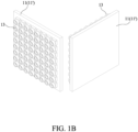
- FIG. 1B is a perspective assembly view of the first embodiment of the AiP verification board of the present disclosure
- the AiP verification board of the present disclosure includes a carrier board, such as an antenna array board 11 provided with an antenna array or an electronic circuit board 11' provided with an electronic circuit, and a plurality of push-on connectors, such as sub-miniature push-on micro (SMPM) connectors 13.
- SMPM sub-miniature push-on micro
- a plurality of SMPM connectors 13 are arranged in an array on one side of the antenna array board 11 or the electronic circuit board 11'.
- the plurality of SMPM connectors 13 are electrically connected with the antenna array board 11 or the electronic circuit board 11' to test the characteristics of the antenna array on the antenna array board 11 or the characteristics of the electronic circuit on the electronic circuit board 11'.
- each of the plurality of SMPM connectors 13 includes a connection pad (not shown in the drawings).
- the antenna array on the antenna array board 11 is a millimeter wave (mmWave) antenna array
- the electronic circuit on the electronic circuit board 11' is a millimeter wave electronic circuit.
- the plurality of SMPM connectors 13 are disposed on a single side of the antenna array board 11 or the electronic circuit board 11', and the plurality of SMPM connectors 13 are arranged in an 8x8 SMPM connector array.
- the plurality of SMPM connectors 13 can be directly and electrically connected with the antenna array board 11 or the electronic circuit board 11'. Therefore, since the plurality of SMPM connectors 13 can be directly connected with the test equipment, this embodiment can test the characteristics of the antenna array of the antenna array board 11 and the characteristics of the electronic components of the electronic circuit board 11' separately through the plurality of SMPM connectors 13, thereby reducing the difficulty of verification of millimeter wave antennas and its circuits.
- the connection pad on each SMPM connector 13 can be designed or optimized into a suitable structure to achieve low-loss conversion.
- the AiP verification board provided with the plurality of SMPM connectors 13 can be fixed on a beamforming test platform, and the present disclosure can divide the AiP into antennas and circuits for separate tests. Therefore, it is not necessary to manufacture various circuit boards and antennas, thereby saving design costs.
- FIG. 2A and FIG. 2B are the perspective exploded view and the perspective assembly view of the second embodiment of the AiP verification board of the present disclosure.
- the AiP verification board of this embodiment includes a carrier board, such as an antenna array board 31 provided with an antenna array or an electronic circuit board 31' provided with an electronic circuit, and a plurality of adaptor structures 33.
- the RDIS Invisipin is taken as an example for the following descriptions for the plurality of adaptor structures 33, but the present disclosure is not limited thereto.
- the plurality of adaptor structures 33 are arranged in an array on one side of the antenna array board 31 or the electronic circuit board 31'.
- An antenna array is disposed on the other side of the antenna array board 31 or an electronic circuit is disposed on the other side of the electronic circuit board 31'.
- the plurality of adaptor structures 33 are electrically connected with the antenna array on the antenna array board 31 or the electronic circuit on the electronic circuit board 31' through ground-signal-ground (GSG) through holes to test the characteristics of the antenna array on the antenna array board 31 or the characteristics of the electronic circuit and components on the electronic circuit board 31'.
- GSG ground-signal-ground
- the antenna array on the antenna array board 31 is a millimeter wave antenna array
- the electronic circuit on the electronic circuit board 31' is a millimeter wave electronic circuit.
- each adaptor structure in the plurality of adaptor structures 33 includes a connection pad 331.
- the plurality of adaptor structures 33 are arranged on one side of the antenna array board 31 or the electronic circuit board 31'.
- the plurality of adaptor structures 33 are arranged into an 8x8 adaptor structure conversion array.
- the plurality of adaptor structures 33 can be directly and electrically connected with the antenna array board 31 or the electronic circuit board 31'. Since the plurality of adaptor structures 33 can also be connected with the test equipment, this embodiment can test the characteristics of the antenna array of the antenna array board 31 and the characteristics of the electronic components of the electronic circuit board 31' separately through the plurality of adaptor structures 33 of the conversion array to reduce the difficulties of verification of millimeter wave antennas and its circuits.
- each adaptor structure 33 can provide a very small cross-section, therefore when connecting to other circuit boards (such as printed circuit boards), the circuit boards only need to have corresponding coaxial pads etched to be directly connected with the AiP verification board of the present disclosure without the need for additional connectors.
- the connection pad on each adaptor structure can be designed or optimized into a suitable structure to achieve low loss conversion.
- the AiP verification board with the plurality of adaptor structures 33 can be fixed on a beamforming test platform, and the present disclosure can divide the AiP into antennas and circuits for separate tests. Therefore, it is not necessary to manufacture various circuit boards and antennas, thereby saving design costs.
- FIG. 3A and FIG. 3B are a perspective exploded view and a perspective assembly view of the third embodiment of the AiP verification board of the present disclosure.
- the AiP verification board of the present disclosure includes a plurality of connectors 51 (for example, SMPM connectors) and a plurality of adaptor structures 53 (for example, Invisipin).
- the plurality of SMPM connectors 51 are arranged in an array on one side of a carrier board (for example, a radio frequency circuit board 55 provided with a radio frequency circuit), and the plurality of adaptor structures 53 are arranged in an array on the other side of the radio frequency circuit board 55.
- the plurality of SMPM connectors 51 can be electrically connected with the plurality of adaptor structures 53 through the ground-signal-ground through holes in the carrier board.
- the plurality of adaptor structures 53 are disposed on one side of the radio frequency circuit board 55, and the plurality of SMPM connectors 51 are disposed on the other side of the radio frequency circuit board 55.
- the plurality of adaptor structures 53 and the plurality of SMPM connectors 51 are arranged into a conversion structure including a 4x4 adaptor structure array and a 4x4 SMPM connector array, wherein each adaptor structure 53 is configured based on the ground-signal-ground (GSG) through holes.
- GSG ground-signal-ground
- the plurality of SMPM connectors 51 of this embodiment can be directly connected with test equipment or instruments, while the plurality of adaptor structures 53 are quickly connected with the device under test (DUT).
- connection pad on each adaptor structure 53 can be designed or optimized into a suitable structure to achieve low loss conversion.
- this embodiment can test the characteristics of the antenna array of the antenna array board and the characteristics of the electronic components of the electronic circuit board separately through the plurality of SMPM connectors 51 and the plurality of adaptor structures 53 to reduce the difficulties of verification of millimeter wave antennas and its circuits.
- the AiP verification board provided with the plurality of SMPM connectors 51 and the plurality of adaptor structures 53 can be fixed on a beamforming test platform, and this embodiment can divide the AiP into antennas and circuits for separate tests. Therefore, it is not necessary to manufacture various circuit boards and antennas, thereby saving design costs.
- a plurality of conversion verification boards provided with SMPM connectors 51 and adaptor structures 53 can be used to test and verify the device under test (for example, antenna array board or electronic circuit board) disposed in the middle, so the application will no longer be limited to the stacking restrictions of the circuit board itself.
- FIG. 4A, FIG. 4B and FIG. 4C are a perspective assembled top view, a perspective assembled bottom view, and a perspective exploded view of the fourth embodiment of the AiP verification board of the present disclosure.
- This embodiment includes a bottom AiP verification board 71, a band-pass filter circuit board 81 and a top AiP verification board 91, wherein the band-pass filter circuit board 81 is disposed between the bottom AiP verification board 71 and the top AiP verification board 91.
- the band-pass filter circuit board 81 can also be replaced with other circuit boards. Alternatively, other circuit boards can be added above and/or below the band-pass filter circuit board 81. In other words, multiple circuit boards can be stacked between the bottom AiP verification board 71 and the top AiP verification board 91 to measure and verify the multiple circuit boards at the same time.
- the bottom AiP verification board 71, the band-pass filter circuit board 81, and the top AiP verification board 91 are stacked in order, and can be fixed on a beamforming test platform 101.
- the beamforming test platform 101 includes a jig body 1011 and a plurality of fixing clamps 1013.
- the aforementioned test platform and clamps are just examples and are not intended to limit the present disclosure.
- the center of the jig body 1011 in the beamforming test platform 101 of this embodiment has an opening 1015 to facilitate testing and verification of the upper sides and the lower sides of the AiP verification boards or the circuit boards disposed on the beamforming test platform 101 through the opening 1015.
- FIG. 5A and FIG. 5B are respectively a perspective view and a partially enlarged perspective view of an upper part of the bottom AiP verification board 71 of this embodiment.
- FIG. 6A and FIG. 6B are respectively a perspective view and a partially enlarged perspective view of a lower part of the bottom AiP verification board 71 of this embodiment.
- the upper part of the bottom AiP verification board 71 has a plurality of adaptor structures 711, and is electrically connected with the lower part of the band-pass filter circuit board 81.
- the plurality of adaptor structures 711 are arranged in an array.
- the lower part of the bottom AiP verification board 71 has a plurality of push-on connectors 713 (for example, SMPM connectors).
- the plurality of the push-on connectors 713 are also arranged in an array.
- the plurality of push-on connectors 713 and the plurality of adaptor structures 711 are electrically connected through ground-signal-ground (GSG) through holes (not shown).
- GSG ground-signal-ground
- FIG. 7A and FIG. 7B are respectively a perspective view and a partially enlarged perspective view of an upper part of the band-pass filter circuit board 81 of this embodiment.
- the upper part of the band-pass filter circuit board 81 has a plurality of adaptor structures 811 and is electrically connected with the lower part of the top AiP verification board 91 above.
- the plurality of adaptor structures 811 are arranged in an array.
- FIG. 8A and FIG. 8B respectively show a perspective view and a partially enlarged perspective view of the lower part of the band-pass filter circuit board 81 of this embodiment. As shown in FIG. 8A and FIG.
- the lower part of the band-pass filter circuit board 81 is a band-pass filter circuit structure 813.
- the lower part of the band-pass filter circuit board 81 is electrically connected with the upper part of the bottom AiP verification board 71 below through ground-signal-ground (GSG) connection pads.
- GSG ground-signal-ground
- FIG. 9A is a perspective view of the upper part of the top AiP verification board 91 of this embodiment, while FIG. 9B and FIG. 9C respectively show a perspective view and a partially enlarged perspective view of the lower part of the top AiP verification board 91 of this embodiment.
- the upper part of the top AiP verification board 91 has a plurality of push-on connectors 911 (such as SMPM connectors).
- the lower part of the top AiP verification board 91 has a plurality of ground-signal-ground (GSG) connection pads 913, and is electrically connected to the upper part of the band-pass filter circuit board 81 below.
- GSG ground-signal-ground
- the aforementioned specific embodiments of the present disclosure can effectively shorten the development time of AiP, that is, the verification board of the present disclosure can be used to quickly swap antennas or circuits for their separate verification and testing, which can greatly shorten the development schedule of AiP.
- the integration of the overall test system can be more flexible in testing.
- the operating frequency bandwidth of a circuit is relatively wide and that of an antenna is relatively narrow, when testing the characteristics of different frequency bands, only the antennas needs to be replaced without the need to redesign and reproduce the circuits. Therefore, the application is broader than traditional test structures.
Landscapes
- Physics & Mathematics (AREA)
- Electromagnetism (AREA)
- Engineering & Computer Science (AREA)
- General Physics & Mathematics (AREA)
- Signal Processing (AREA)
- Computer Networks & Wireless Communication (AREA)
- General Engineering & Computer Science (AREA)
- Variable-Direction Aerials And Aerial Arrays (AREA)
- Aerials With Secondary Devices (AREA)
- Production Of Multi-Layered Print Wiring Board (AREA)
- Structure Of Printed Boards (AREA)
- Microelectronics & Electronic Packaging (AREA)
- Support Of Aerials (AREA)
Description
- The present disclosure relates to verification and test of antennas-in-package (AiP). In particular, the present disclosure relates to an AiP verification board suitable for millimeter wave (mmWave) 5G mobile communication.
- Antennas-in-package (AiP) is a technology for integrating one or more antennas and transceivers into a standard surface-mount device. It has been widely used in 60 GHz gesture sensors, 77 GHz automobile radars, 94 GHz phased arrays, or even image sensors up to 122 GHz and wireless networks up to 300 GHz. In addition, because the fifth-generation mobile communication (5G) millimeter wave spectrum uses millimeter waves as carriers, it has sufficient bandwidth to provide next-generation user experiences and industrial applications, and AiP technology is gradually moving towards the development direction of 5G millimeter wave.
- Nowadays, in the design of AiP, the upper layer of the circuit board is an antenna array, and the lower layer usually includes electronic circuits and electronic components. Therefore, usually the antenna array cannot be verified or tested alone, thus verification and test of electrical characteristics are possible only for the entire AiP system, which results in blind spots in the development and test of AiP.
- Therefore, how to provide a verification board that can individually test antenna arrays, electronic circuits, electronic components and can combine antennas and electronic components at the same time to overcome the difficulties of AiP verification and reduce the time and cost of AiP development is one of the urgent issues in the art.
- Publication
US 2015 369840 A1 andEP 1 542 028 A1 discuss information that may be regarded as useful for understanding the background of the related art. - In order to solve the above problems, an embodiment of the present disclosure provides an AiP verification board according to the independent claims.
- The invention is set out in the appended set of claims.
- The drawings are incorporated in the present disclosure and constitute a part of the present disclosure to show various specific embodiments of the present disclosure and illustrate specific embodiments of the present disclosure.
-
FIG. 1A is a perspective exploded view of the first embodiment of an AiP verification board of the present disclosure. -
FIG. 1B is a perspective assembly view of the first embodiment of an AiP -
FIG. 2A is a perspective exploded view of the second embodiment of an AiP verification board of the present disclosure. -
FIG. 2B is a perspective assembly view of the second embodiment of an AiP verification board of the present disclosure. -
FIG. 2C is a perspective schematic diagram of an adaptor structure of the second embodiment of an AiP verification board of the present disclosure. -
FIG. 3A is a perspective exploded view of the third embodiment of an AiP verification board of the present disclosure. -
FIG. 3B is a perspective assembly view of the third embodiment of an AiP verification board of the present disclosure. -
FIG. 4A is a perspective assembly top view of the fourth embodiment of an AiP verification board of the present disclosure. -
FIG. 4B is a perspective assembly bottom view of the fourth embodiment of an AiP verification board of the present disclosure. -
FIG. 4C is a perspective exploded view of the fourth embodiment of an AiP verification board of the present disclosure. -
FIG. 5A is a perspective view of an upper part of a bottom AiP verification board of the fourth embodiment of an AiP verification board of the present disclosure. -
FIG. 5B is a partially enlarged perspective view of an upper part of a bottom AiP verification board of the fourth embodiment of an AiP verification board of the present disclosure. -
FIG. 6A is a perspective view of a lower part of a bottom AiP verification board of the fourth embodiment of an AiP verification board of the present disclosure. -
FIG. 6B is a partially enlarged perspective view of a lower part of a bottom AiP verification board of the fourth embodiment of an AiP verification board of the present disclosure. -
FIG. 7A is a perspective view of an upper part of a band-pass filter circuit board of the fourth embodiment of an AiP verification board of the present disclosure. -
FIG. 7B is a partially enlarged perspective view of an upper part of a band-pass filter circuit board of the fourth embodiment of an AiP verification board of the present disclosure. -
FIG. 8A is a perspective view of a lower part of a band-pass filter circuit board of the fourth embodiment of an AiP verification board of the present disclosure. -
FIG. 8B is a partially enlarged perspective view of a lower part of a band-pass filter circuit board of the fourth embodiment of an AiP verification board of the present disclosure. -
FIG. 9A is a perspective view of an upper part of a top AiP verification board of the fourth embodiment of an AiP verification board of the present disclosure. -
FIG. 9B is a perspective view of a lower part of a top AiP verification board of the fourth embodiment of an AiP verification board of the present disclosure. -
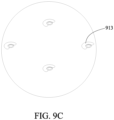
FIG. 9C is a partially enlarged perspective view of a lower part of a top AiP verification board of the fourth embodiment of an AiP verification board of the present disclosure. - The following specific embodiments illustrate the implementation of the present disclosure. Those skilled in the art can easily understand the other advantages and effects of the present disclosure based on the contents disclosed in this specification, and can also implement or apply the present disclosure through the other different specific embodiments.
- In order to solve the aforementioned disadvantages of the conventional technology, the purpose of the present disclosure is to provide an AiP verification board suitable for millimeter wave (mmWave) fifth-generation mobile communications (5G). The specific embodiments of the present disclosure are described as follows.
-
FIG. 1A is a perspective exploded view of the first embodiment of an AiP verification board of the present disclosure, andFIG. 1B is a perspective assembly view of the first embodiment of the AiP verification board of the present disclosure. The AiP verification board of the present disclosure includes a carrier board, such as anantenna array board 11 provided with an antenna array or an electronic circuit board 11' provided with an electronic circuit, and a plurality of push-on connectors, such as sub-miniature push-on micro (SMPM)connectors 13. A plurality ofSMPM connectors 13 are arranged in an array on one side of theantenna array board 11 or the electronic circuit board 11'. The plurality ofSMPM connectors 13 are electrically connected with theantenna array board 11 or the electronic circuit board 11' to test the characteristics of the antenna array on theantenna array board 11 or the characteristics of the electronic circuit on the electronic circuit board 11'. - In an embodiment, each of the plurality of
SMPM connectors 13 includes a connection pad (not shown in the drawings). The antenna array on theantenna array board 11 is a millimeter wave (mmWave) antenna array, and the electronic circuit on the electronic circuit board 11' is a millimeter wave electronic circuit. - As shown in
FIGs. 1A and1B , the plurality ofSMPM connectors 13 are disposed on a single side of theantenna array board 11 or the electronic circuit board 11', and the plurality ofSMPM connectors 13 are arranged in an 8x8 SMPM connector array. The plurality ofSMPM connectors 13 can be directly and electrically connected with theantenna array board 11 or the electronic circuit board 11'. Therefore, since the plurality ofSMPM connectors 13 can be directly connected with the test equipment, this embodiment can test the characteristics of the antenna array of theantenna array board 11 and the characteristics of the electronic components of the electronic circuit board 11' separately through the plurality ofSMPM connectors 13, thereby reducing the difficulty of verification of millimeter wave antennas and its circuits. It is worth mentioning that the connection pad on eachSMPM connector 13 can be designed or optimized into a suitable structure to achieve low-loss conversion. - In an embodiment, the AiP verification board provided with the plurality of
SMPM connectors 13 can be fixed on a beamforming test platform, and the present disclosure can divide the AiP into antennas and circuits for separate tests. Therefore, it is not necessary to manufacture various circuit boards and antennas, thereby saving design costs. - Please refer to
FIG. 2A andFIG. 2B , which are the perspective exploded view and the perspective assembly view of the second embodiment of the AiP verification board of the present disclosure. The AiP verification board of this embodiment includes a carrier board, such as anantenna array board 31 provided with an antenna array or an electronic circuit board 31' provided with an electronic circuit, and a plurality ofadaptor structures 33. The RDIS Invisipin is taken as an example for the following descriptions for the plurality ofadaptor structures 33, but the present disclosure is not limited thereto. The plurality ofadaptor structures 33 are arranged in an array on one side of theantenna array board 31 or the electronic circuit board 31'. An antenna array is disposed on the other side of theantenna array board 31 or an electronic circuit is disposed on the other side of the electronic circuit board 31'. The plurality ofadaptor structures 33 are electrically connected with the antenna array on theantenna array board 31 or the electronic circuit on the electronic circuit board 31' through ground-signal-ground (GSG) through holes to test the characteristics of the antenna array on theantenna array board 31 or the characteristics of the electronic circuit and components on the electronic circuit board 31'. In addition, the antenna array on theantenna array board 31 is a millimeter wave antenna array, and the electronic circuit on the electronic circuit board 31' is a millimeter wave electronic circuit. - In an embodiment, as shown in
FIG. 2C , each adaptor structure in the plurality ofadaptor structures 33 includes aconnection pad 331. - As shown in
FIG. 2A andFIG. 2B , the plurality ofadaptor structures 33 are arranged on one side of theantenna array board 31 or the electronic circuit board 31'. The plurality ofadaptor structures 33 are arranged into an 8x8 adaptor structure conversion array. The plurality ofadaptor structures 33 can be directly and electrically connected with theantenna array board 31 or the electronic circuit board 31'. Since the plurality ofadaptor structures 33 can also be connected with the test equipment, this embodiment can test the characteristics of the antenna array of theantenna array board 31 and the characteristics of the electronic components of the electronic circuit board 31' separately through the plurality ofadaptor structures 33 of the conversion array to reduce the difficulties of verification of millimeter wave antennas and its circuits. It is worth mentioning that since eachadaptor structure 33 can provide a very small cross-section, therefore when connecting to other circuit boards (such as printed circuit boards), the circuit boards only need to have corresponding coaxial pads etched to be directly connected with the AiP verification board of the present disclosure without the need for additional connectors. In addition, the connection pad on each adaptor structure can be designed or optimized into a suitable structure to achieve low loss conversion. - In an embodiment, the AiP verification board with the plurality of
adaptor structures 33 can be fixed on a beamforming test platform, and the present disclosure can divide the AiP into antennas and circuits for separate tests. Therefore, it is not necessary to manufacture various circuit boards and antennas, thereby saving design costs. - Please refer to
FIG. 3A andFIG. 3B , which are a perspective exploded view and a perspective assembly view of the third embodiment of the AiP verification board of the present disclosure. The AiP verification board of the present disclosure includes a plurality of connectors 51 (for example, SMPM connectors) and a plurality of adaptor structures 53 (for example, Invisipin). - The plurality of
SMPM connectors 51 are arranged in an array on one side of a carrier board (for example, a radiofrequency circuit board 55 provided with a radio frequency circuit), and the plurality ofadaptor structures 53 are arranged in an array on the other side of the radiofrequency circuit board 55. The plurality ofSMPM connectors 51 can be electrically connected with the plurality ofadaptor structures 53 through the ground-signal-ground through holes in the carrier board. - In an embodiment, as shown in
FIGs. 3A and3B , the plurality ofadaptor structures 53 are disposed on one side of the radiofrequency circuit board 55, and the plurality ofSMPM connectors 51 are disposed on the other side of the radiofrequency circuit board 55. The plurality ofadaptor structures 53 and the plurality ofSMPM connectors 51 are arranged into a conversion structure including a 4x4 adaptor structure array and a 4x4 SMPM connector array, wherein eachadaptor structure 53 is configured based on the ground-signal-ground (GSG) through holes. In other words, the plurality ofSMPM connectors 51 of this embodiment can be directly connected with test equipment or instruments, while the plurality ofadaptor structures 53 are quickly connected with the device under test (DUT). Therefore, the device under test only needs to have corresponding coaxial pads etched to be directly connected with the plurality of adaptor structures on the AiP verification board of the present disclosure, without the need for additional connectors. It is worth mentioning that the connection pad on eachadaptor structure 53 can be designed or optimized into a suitable structure to achieve low loss conversion. - It is worth mentioning that since the plurality of
SMPM connectors 51 can be directly connected with test equipment or instruments and the device under test does not require additional connectors or adaptor structures, this embodiment can test the characteristics of the antenna array of the antenna array board and the characteristics of the electronic components of the electronic circuit board separately through the plurality ofSMPM connectors 51 and the plurality ofadaptor structures 53 to reduce the difficulties of verification of millimeter wave antennas and its circuits. - In an embodiment, the AiP verification board provided with the plurality of
SMPM connectors 51 and the plurality ofadaptor structures 53 can be fixed on a beamforming test platform, and this embodiment can divide the AiP into antennas and circuits for separate tests. Therefore, it is not necessary to manufacture various circuit boards and antennas, thereby saving design costs. - In an embodiment, it is worth noting that a plurality of conversion verification boards provided with
SMPM connectors 51 andadaptor structures 53 can be used to test and verify the device under test (for example, antenna array board or electronic circuit board) disposed in the middle, so the application will no longer be limited to the stacking restrictions of the circuit board itself. - Please refer to
FIG. 4A, FIG. 4B andFIG. 4C , which are a perspective assembled top view, a perspective assembled bottom view, and a perspective exploded view of the fourth embodiment of the AiP verification board of the present disclosure. This embodiment includes a bottomAiP verification board 71, a band-passfilter circuit board 81 and a topAiP verification board 91, wherein the band-passfilter circuit board 81 is disposed between the bottomAiP verification board 71 and the topAiP verification board 91. The band-passfilter circuit board 81 can also be replaced with other circuit boards. Alternatively, other circuit boards can be added above and/or below the band-passfilter circuit board 81. In other words, multiple circuit boards can be stacked between the bottomAiP verification board 71 and the topAiP verification board 91 to measure and verify the multiple circuit boards at the same time. - In an embodiment, the bottom
AiP verification board 71, the band-passfilter circuit board 81, and the topAiP verification board 91 are stacked in order, and can be fixed on abeamforming test platform 101. Thebeamforming test platform 101 includes ajig body 1011 and a plurality of fixingclamps 1013. The aforementioned test platform and clamps are just examples and are not intended to limit the present disclosure. In addition, the center of thejig body 1011 in thebeamforming test platform 101 of this embodiment has anopening 1015 to facilitate testing and verification of the upper sides and the lower sides of the AiP verification boards or the circuit boards disposed on thebeamforming test platform 101 through theopening 1015. -
FIG. 5A and FIG. 5B are respectively a perspective view and a partially enlarged perspective view of an upper part of the bottomAiP verification board 71 of this embodiment.FIG. 6A and FIG. 6B are respectively a perspective view and a partially enlarged perspective view of a lower part of the bottomAiP verification board 71 of this embodiment. As shown inFIGs. 4C ,5A ,5B ,6A and 6B , the upper part of the bottomAiP verification board 71 has a plurality ofadaptor structures 711, and is electrically connected with the lower part of the band-passfilter circuit board 81. The plurality ofadaptor structures 711 are arranged in an array. The lower part of the bottomAiP verification board 71 has a plurality of push-on connectors 713 (for example, SMPM connectors). The plurality of the push-onconnectors 713 are also arranged in an array. The plurality of push-onconnectors 713 and the plurality ofadaptor structures 711 are electrically connected through ground-signal-ground (GSG) through holes (not shown). -
FIG. 7A and FIG. 7B are respectively a perspective view and a partially enlarged perspective view of an upper part of the band-passfilter circuit board 81 of this embodiment. As shown inFIG. 7A and FIG. 7B , the upper part of the band-passfilter circuit board 81 has a plurality ofadaptor structures 811 and is electrically connected with the lower part of the topAiP verification board 91 above. The plurality ofadaptor structures 811 are arranged in an array.FIG. 8A and FIG. 8B respectively show a perspective view and a partially enlarged perspective view of the lower part of the band-passfilter circuit board 81 of this embodiment. As shown inFIG. 8A and FIG. 8B , the lower part of the band-passfilter circuit board 81 is a band-passfilter circuit structure 813. The lower part of the band-passfilter circuit board 81 is electrically connected with the upper part of the bottomAiP verification board 71 below through ground-signal-ground (GSG) connection pads. -
FIG. 9A is a perspective view of the upper part of the topAiP verification board 91 of this embodiment, whileFIG. 9B andFIG. 9C respectively show a perspective view and a partially enlarged perspective view of the lower part of the topAiP verification board 91 of this embodiment. As shown inFIGs. 9A, 9B and9C , the upper part of the topAiP verification board 91 has a plurality of push-on connectors 911 (such as SMPM connectors). The lower part of the topAiP verification board 91 has a plurality of ground-signal-ground (GSG)connection pads 913, and is electrically connected to the upper part of the band-passfilter circuit board 81 below. - In summary, the aforementioned specific embodiments of the present disclosure can effectively shorten the development time of AiP, that is, the verification board of the present disclosure can be used to quickly swap antennas or circuits for their separate verification and testing, which can greatly shorten the development schedule of AiP. In addition, the integration of the overall test system can be more flexible in testing. Moreover, since the operating frequency bandwidth of a circuit is relatively wide and that of an antenna is relatively narrow, when testing the characteristics of different frequency bands, only the antennas needs to be replaced without the need to redesign and reproduce the circuits. Therefore, the application is broader than traditional test structures.
- The aforementioned embodiments are exemplary to illustrate the technical principles, features and effects of the present disclosure, and are not intended to limit the implementable scope of the present disclosure. The scope of protection of the rights of the present disclosure should be as recited in the following claims.
Claims (12)
- An antennas-in-package, AiP, verification board, comprising:a carrier board (11, 11') configured for disposing an antenna array or an electronic circuit; anda plurality of push-on connectors (13) arranged in an array on the carrier board (11, 11'),wherein the plurality of push-on connectors (13) are configured to be electrically connected with the antenna array or the electronic circuit on the carrier board (11, 11') for testing characteristics of the antenna array on the carrier board or characteristics of the electronic circuit on the carrier board (11, 11'),wherein the plurality of push-on connectors (13) are configured to be connected with a test equipment, characterised in that the plurality of push-on connectors (13) are sub-miniature push-on micro, SMPM, connectors (13).
- The AiP verification board of claim 1, wherein each of the plurality of push-on connectors (13) comprises a connection pad.
- The AiP verification board of claim 1, wherein the antenna array is a millimeter wave, mmWave, antenna array, and the electronic circuit is a millimeter wave electronic circuit.
- A beamforming test platform (101) comprising the AiP verification board according to claim 1.
- An antennas-in-package (AiP) verification board, comprising:a carrier board (31, 31') configured for disposing an antenna array or an electronic circuit;a plurality of through holes with a ground-signal-ground, GSG, configuration formed in an array in the carrier board (31, 31'); anda plurality of adaptor structures (33) arranged in an array on the carrier board (31, 31'),wherein the plurality of adaptor structures (33) are configured to be electrically connected with the antenna array on the carrier board (31, 31') or the electronic circuit on the carrier board (31, 31') through the through hole with the GSG configuration for testing characteristics of the antenna array on the carrier board (31, 31') or characteristics of the electronic circuit on the carrier board (31, 31'),wherein the plurality of adaptor structures (33) are configured to be connected with a test equipment, characterised in thatthe plurality of adaptor structures (33) are Invisipins
- The AiP verification board of claim 5, wherein the antenna array is a millimeter wave, mmWave, antenna array, and the electronic circuit is a millimeter wave electronic circuit.
- A beamforming test platform (101) comprising the AiP verification board according to claim 5.
- An antennas-in-package, AiP, verification board, comprising:a carrier board (55) configured for disposing a radio frequency circuit;a plurality of through holes with a ground-signal-ground (GSG) configuration formed in an array in the carrier board (55);a plurality of connectors (51) arranged in an array on one side of the carrier board (55); anda plurality of adaptor structures (53) arranged in an array on another side of the carrier board (55),wherein the plurality of connectors (51) are electrically connected with the plurality of adaptor structures (53) through the through holes with the GSG configuration, andwherein the plurality of connectors (51) are sub-miniature push-on micro, SMPM, connectors (51).
- The AiP verification board of claim 8, wherein the plurality of connectors (51) are configured to be connected with a test equipment, and the plurality of adaptor structures (53) are configured to be connected with a device under test.
- The AiP verification board of claim 8, wherein the plurality of connectors (51) or the plurality of adaptor structures (53) are configured to be connected with a circuit board.
- The AiP verification board of claim 9, wherein the device under test is a millimeter wave, mmWave, antenna array or a millimeter wave electronic circuit.
- A beamforming test platform (101) comprising the AiP verification board according to claim 8.
Applications Claiming Priority (1)
| Application Number | Priority Date | Filing Date | Title |
|---|---|---|---|
| US201962887815P | 2019-08-16 | 2019-08-16 |
Publications (2)
| Publication Number | Publication Date |
|---|---|
| EP3780275A1 EP3780275A1 (en) | 2021-02-17 |
| EP3780275B1 true EP3780275B1 (en) | 2023-07-19 |
Family
ID=72087893
Family Applications (3)
| Application Number | Title | Priority Date | Filing Date |
|---|---|---|---|
| EP20191023.9A Active EP3780259B1 (en) | 2019-08-16 | 2020-08-14 | Transition structure and multilayer transition structure for millimeter wave |
| EP20191147.6A Active EP3779477B1 (en) | 2019-08-16 | 2020-08-14 | Rapid over-the-air production line test platform |
| EP20191138.5A Active EP3780275B1 (en) | 2019-08-16 | 2020-08-14 | Antennas-in-package verification board |
Family Applications Before (2)
| Application Number | Title | Priority Date | Filing Date |
|---|---|---|---|
| EP20191023.9A Active EP3780259B1 (en) | 2019-08-16 | 2020-08-14 | Transition structure and multilayer transition structure for millimeter wave |
| EP20191147.6A Active EP3779477B1 (en) | 2019-08-16 | 2020-08-14 | Rapid over-the-air production line test platform |
Country Status (5)
| Country | Link |
|---|---|
| US (4) | US11316240B2 (en) |
| EP (3) | EP3780259B1 (en) |
| JP (4) | JP7179803B2 (en) |
| CN (3) | CN112394233B (en) |
| TW (3) | TWI748579B (en) |
Families Citing this family (17)
| Publication number | Priority date | Publication date | Assignee | Title |
|---|---|---|---|---|
| US11536760B2 (en) * | 2017-11-28 | 2022-12-27 | Ase Test, Inc. | Testing device, testing system, and testing method |
| TWI748579B (en) * | 2019-08-16 | 2021-12-01 | 稜研科技股份有限公司 | Transition structure and multilayer transition structure for millimeter wave |
| EP4145149A1 (en) | 2021-09-07 | 2023-03-08 | TMY Technology Inc. | Broadband measurement system and measurement method for broadband property |
| USD1057752S1 (en) * | 2021-10-08 | 2025-01-14 | Life Technologies Corporation | Display panel of an electroporation device with a graphical user interface |
| CN116112593B (en) * | 2021-11-10 | 2026-01-02 | 深圳市计量质量检测研究院(国家高新技术计量站丶国家数字电子产品质量监督检验中心) | Clamping device for OTA testing |
| TWI800098B (en) | 2021-11-15 | 2023-04-21 | 貿聯國際股份有限公司 | Testing board |
| EP4180833A1 (en) * | 2021-11-16 | 2023-05-17 | TMY Technology Inc. | Method for measuring angle of arrival with phased array |
| CN116137393A (en) * | 2021-11-17 | 2023-05-19 | 贸联电子(昆山)有限公司 | test board |
| US11969351B2 (en) | 2022-02-03 | 2024-04-30 | James M. Jackson | Systems and methods for magnetic joints |
| USD1044834S1 (en) * | 2022-03-29 | 2024-10-01 | Tmy Technology Inc. | Display screen or portion thereof with graphical user interface |
| USD1044833S1 (en) * | 2022-03-29 | 2024-10-01 | Tmy Technology Inc. | Display screen or portion thereof with graphical user interface |
| USD1046883S1 (en) * | 2022-03-29 | 2024-10-15 | Tmy Technology Inc. | Display screen or portion thereof with graphical user interface |
| USD1046884S1 (en) * | 2022-04-25 | 2024-10-15 | Tmy Technology Inc. | Display screen or portion thereof with graphical user interface |
| USD1048052S1 (en) * | 2022-05-23 | 2024-10-22 | Tmy Technology Inc. | Display screen or portion thereof with graphical user interface |
| US12451611B2 (en) * | 2022-06-01 | 2025-10-21 | United States Of America As Represented By The Secretary Of The Air Force | 3D printed metallic dual-polarized vivaldi arrays on square and triangular lattices |
| TWI816468B (en) * | 2022-07-14 | 2023-09-21 | 國立臺灣大學 | Array RF system |
| US12542351B2 (en) * | 2023-09-26 | 2026-02-03 | Silicon Laboratories Inc. | Automated AoX test system |
Citations (1)
| Publication number | Priority date | Publication date | Assignee | Title |
|---|---|---|---|---|
| EP2469660A2 (en) * | 2010-12-22 | 2012-06-27 | Tyco Electronics Corporation | RF module |
Family Cites Families (66)
| Publication number | Priority date | Publication date | Assignee | Title |
|---|---|---|---|---|
| JPS61239701A (en) * | 1985-04-16 | 1986-10-25 | Mitsubishi Electric Corp | Triplet line type t branch |
| JP2621703B2 (en) * | 1991-09-06 | 1997-06-18 | 日本電気株式会社 | Composite feed radar antenna |
| RU2125275C1 (en) * | 1997-05-06 | 1999-01-20 | Акционерное общество открытого типа Нижегородский авиастроительный завод "Сокол" | Target simulator |
| JP2000216630A (en) | 1999-01-20 | 2000-08-04 | Alps Electric Co Ltd | Transmitter-receiver with antenna |
| JP2001308547A (en) * | 2000-04-27 | 2001-11-02 | Sharp Corp | High frequency multilayer circuit board |
| JP4734723B2 (en) | 2001-01-31 | 2011-07-27 | 凸版印刷株式会社 | Manufacturing method of multilayer wiring board using coaxial via hole |
| US7024165B2 (en) * | 2001-06-14 | 2006-04-04 | Honeywell Federal Manufacturing & Technologies, Llc | ISM band to U-NII band frequency transverter and method of frequency transversion |
| DE10137838A1 (en) * | 2001-08-02 | 2003-02-13 | Philips Corp Intellectual Pty | GPS receiver module |
| JP2003204209A (en) * | 2002-01-07 | 2003-07-18 | Kyocera Corp | High frequency wiring board |
| JP2004108898A (en) * | 2002-09-17 | 2004-04-08 | Advantest Corp | Performance board and test system |
| JP4545606B2 (en) * | 2005-02-04 | 2010-09-15 | 三菱電機株式会社 | Radar cross section measuring device |
| US20060226928A1 (en) * | 2005-04-08 | 2006-10-12 | Henning Larry C | Ball coax interconnect |
| US7965986B2 (en) * | 2006-06-07 | 2011-06-21 | Ets-Lindgren, L.P. | Systems and methods for over-the-air testing of wireless systems |
| KR100926561B1 (en) * | 2007-09-19 | 2009-11-12 | 한국전자통신연구원 | Finite Distance Antenna Radiation Pattern Measurement Apparatus and Method |
| CN101217322A (en) * | 2008-01-16 | 2008-07-09 | 中兴通讯股份有限公司 | Test system and test method for over-the-air performance of wireless USB modem |
| US8842054B2 (en) * | 2008-12-12 | 2014-09-23 | Nanyang Technological University | Grid array antennas and an integration structure |
| JP5474949B2 (en) | 2009-05-12 | 2014-04-16 | パナソニック株式会社 | Antenna evaluation apparatus and antenna evaluation method |
| EP2438699A4 (en) * | 2009-06-03 | 2015-01-21 | Elektrobit System Test Oy | TEST IN RADIO LINK |
| DE102009037336B4 (en) * | 2009-08-14 | 2024-10-31 | Rosenberger Hochfrequenztechnik Gmbh & Co. Kg | Antenna characterization in a waveguide |
| CN102104200B (en) * | 2010-10-28 | 2013-09-25 | 华南理工大学 | Curve array feed source bifocal parabolic reflector space power synthesis antenna |
| US9671445B2 (en) * | 2013-03-15 | 2017-06-06 | Litepoint Corporation | System and method for testing radio frequency wireless signal transceivers using wireless test signals |
| DE102013102714A1 (en) * | 2013-03-18 | 2014-09-18 | Schott Ag | Radio frequency feedthrough |
| CN103297161B (en) * | 2013-05-28 | 2016-03-02 | 惠州Tcl移动通信有限公司 | A kind of terminal antenna receiving sensitivity method of testing and system |
| US9154972B2 (en) * | 2013-06-12 | 2015-10-06 | Apple Inc. | Methods and apparatus for testing electronic devices with antenna arrays |
| JP6402962B2 (en) | 2013-07-17 | 2018-10-10 | パナソニックIpマネジメント株式会社 | High frequency module |
| JP6417329B2 (en) * | 2013-10-01 | 2018-11-07 | ソニーセミコンダクタソリューションズ株式会社 | Connector device and communication system |
| EP3095159A4 (en) | 2014-01-17 | 2017-09-27 | Nuvotronics, Inc. | Wafer scale test interface unit: low loss and high isolation devices and methods for high speed and high density mixed signal interconnects and contactors |
| US10037933B2 (en) * | 2014-06-20 | 2018-07-31 | Xcerra Corporation | Test socket assembly and related methods |
| CN204243214U (en) * | 2014-10-28 | 2015-04-01 | 中兴通讯股份有限公司 | A kind of intelligent antenna equipment |
| CN105634627B (en) * | 2014-10-28 | 2021-04-02 | 中兴通讯股份有限公司 | An antenna array coupling calibration network device and calibration method |
| TWI540792B (en) * | 2014-11-14 | 2016-07-01 | 亞東技術學院 | A far-field calibration system of an antenna arrary system |
| US10297923B2 (en) | 2014-12-12 | 2019-05-21 | The Boeing Company | Switchable transmit and receive phased array antenna |
| CA2913777A1 (en) * | 2014-12-15 | 2016-06-15 | University Of Windsor | Shielded rf transmission lines in low temperature co-fired ceramic constructs and method of making same |
| EP3182144B1 (en) * | 2015-04-10 | 2019-11-06 | General Test Systems Inc. | Wireless terminal testing system and method for controlling same |
| CN106291145B (en) * | 2015-05-12 | 2019-03-01 | 深圳市通用测试系统有限公司 | Wireless Terminal Test System |
| ES2843513T3 (en) * | 2015-12-16 | 2021-07-19 | Ranlos Ab | Method and apparatus for testing wireless communication with vehicles |
| CN106936524B (en) * | 2015-12-31 | 2023-03-31 | 深圳市通用测试系统有限公司 | Test system of wireless terminal |
| TWI594502B (en) * | 2016-03-10 | 2017-08-01 | Nat Chung-Shan Inst Of Science And Tech | Millimeter wave antenna device and its millimeter wave antenna array device |
| CN109075839B (en) * | 2016-04-26 | 2021-10-12 | 梁平 | Over-the-air transmission channel state information acquisition for large MIMO channel emulators with over-the-air transmission connections |
| DE102016111884B4 (en) * | 2016-06-29 | 2024-08-22 | Infineon Technologies Ag | Apparatus, system and method for automatically testing integrated antennas |
| US11750303B2 (en) * | 2016-06-30 | 2023-09-05 | Keysight Technologies, Inc. | Compact system for characterizing a device under test (DUT) having integrated antenna array |
| US10085162B2 (en) * | 2016-07-22 | 2018-09-25 | Ets-Lindgren, Inc. | System and method for over-the-air testing of milli-meter wave and other beamforming technologies |
| CN106159404B (en) * | 2016-09-29 | 2019-10-11 | 上海航天测控通信研究所 | A kind of non-uniform microstrip line is to strip line transition structure |
| SE540655C2 (en) * | 2017-03-06 | 2018-10-09 | Bluetest Ab | Arrangement and method for measuring the performance of devices with wireless capability |
| CN108966264B (en) * | 2017-05-22 | 2023-05-02 | 是德科技股份有限公司 | System and method for performing over-the-air testing for large-scale multiple-input multiple-output wireless systems |
| US20190013830A1 (en) * | 2017-07-10 | 2019-01-10 | Smart Medical Devices, Inc. | Sterilizable wireless communication devices |
| TWI635290B (en) * | 2017-07-11 | 2018-09-11 | 川升股份有限公司 | Antenna radiation pattern measurement system for multipath scenario application |
| IT201700086529A1 (en) * | 2017-07-27 | 2019-01-27 | Thales Alenia Space Italia Spa Con Unico Socio | MICROWAVE ANTENNA MODULE FOR SPACE APPLICATIONS INCLUDING A MODULE TRANSMIT / RECEIVE TYPICAL HYBRID PACKAGE ON PACKAGE |
| CN107834233B (en) * | 2017-09-27 | 2019-04-02 | 中国电子科技集团公司第二十九研究所 | A kind of vertical transition structure |
| CN111226348B (en) * | 2017-10-17 | 2022-03-11 | 康普技术有限责任公司 | Vertical transition for microwave and millimeter-wave communication systems with multilayer substrates |
| US10462686B2 (en) * | 2017-10-23 | 2019-10-29 | Keysight Technologies, Inc. | Over the air (OTA) beamforming testing with a reduced number of receivers |
| KR102387939B1 (en) * | 2017-11-28 | 2022-04-19 | 삼성전자주식회사 | An antenna and an electronic device comprising the antenna |
| US10809296B2 (en) * | 2017-11-28 | 2020-10-20 | Rohde & Schwarz Gmbh & Co. Kg | Over-the-air test system and method for testing a device under test |
| US10756828B2 (en) * | 2017-12-11 | 2020-08-25 | RF DSP Inc. | Millimeter wave RF channel emulator |
| WO2019133097A1 (en) * | 2017-12-29 | 2019-07-04 | Xcerra Corporation | Test socket assembly with antenna and related methods |
| US10916854B2 (en) * | 2018-03-29 | 2021-02-09 | Mediatek Inc. | Antenna structure with integrated coupling element and semiconductor package using the same |
| CN108598690B (en) * | 2018-03-29 | 2024-02-20 | 广东通宇通讯股份有限公司 | Millimeter wave Massive MIMO antenna unit and array antenna |
| CN109100639A (en) * | 2018-09-13 | 2018-12-28 | 苏州永安丰新能源科技有限公司 | A kind of OTA test device and method for communication device context adaptive testing |
| US10725080B2 (en) * | 2018-09-25 | 2020-07-28 | National Instruments Corporation | Correlation of device-under-test orientations and radio frequency measurements |
| TWM581775U (en) * | 2018-11-23 | 2019-08-01 | 耀登科技股份有限公司 | High-frequency antenna device |
| CN109889239B (en) * | 2019-03-27 | 2020-12-08 | 北京邮电大学 | A dual-anechoic chamber structure and testing method for MIMO OTA testing |
| TWI720535B (en) * | 2019-07-08 | 2021-03-01 | 中華精測科技股份有限公司 | Integrated circuit with antenna in package testing apparatus |
| TWI748579B (en) * | 2019-08-16 | 2021-12-01 | 稜研科技股份有限公司 | Transition structure and multilayer transition structure for millimeter wave |
| CN111416200B (en) * | 2020-04-16 | 2025-01-28 | 中国电子科技集团公司第五十四研究所 | Circularly polarized package antenna |
| US11695206B2 (en) * | 2020-06-01 | 2023-07-04 | United States Of America As Represented By The Secretary Of The Air Force | Monolithic decade-bandwidth ultra-wideband antenna array module |
| US12188970B2 (en) * | 2020-09-25 | 2025-01-07 | Tron Future Tech Inc. | Near-field testing apparatus for testing antenna array and related method |
-
2020
- 2020-07-24 TW TW109125128A patent/TWI748579B/en active
- 2020-07-24 CN CN202010723854.8A patent/CN112394233B/en active Active
- 2020-07-24 TW TW109125126A patent/TWI741695B/en active
- 2020-07-24 CN CN202010725266.8A patent/CN112397863B/en active Active
- 2020-08-12 TW TW109127363A patent/TWI751645B/en active
- 2020-08-12 CN CN202010806834.7A patent/CN112394234B/en active Active
- 2020-08-13 JP JP2020136687A patent/JP7179803B2/en active Active
- 2020-08-13 JP JP2020136688A patent/JP7062219B2/en active Active
- 2020-08-13 US US16/992,170 patent/US11316240B2/en active Active
- 2020-08-14 EP EP20191023.9A patent/EP3780259B1/en active Active
- 2020-08-14 EP EP20191147.6A patent/EP3779477B1/en active Active
- 2020-08-14 EP EP20191138.5A patent/EP3780275B1/en active Active
- 2020-08-14 JP JP2020136970A patent/JP7074811B2/en active Active
- 2020-08-14 US US16/993,351 patent/US11682818B2/en active Active
- 2020-08-14 US US16/993,348 patent/US11205827B2/en active Active
-
2021
- 2021-10-13 US US17/500,928 patent/US11600894B2/en active Active
-
2022
- 2022-01-06 JP JP2022001172A patent/JP7329085B2/en active Active
Patent Citations (1)
| Publication number | Priority date | Publication date | Assignee | Title |
|---|---|---|---|---|
| EP2469660A2 (en) * | 2010-12-22 | 2012-06-27 | Tyco Electronics Corporation | RF module |
Non-Patent Citations (1)
| Title |
|---|
| A A A: "Invisipin Board to Board", 31 December 2019 (2019-12-31), XP055982885, Retrieved from the Internet <URL:https://www.rdis.com/assets/downloads/Invisipin-Board-to-Board-Spec-Sheet-.pdf> [retrieved on 20221118] * |
Also Published As
Similar Documents
| Publication | Publication Date | Title |
|---|---|---|
| US11682818B2 (en) | Antennas-in-package verification board | |
| US6417747B1 (en) | Low cost, large scale RF hybrid package for simple assembly onto mixed signal printed wiring boards | |
| US7042412B2 (en) | Printed dual dipole antenna | |
| US20210242569A1 (en) | Wiring substrate, antenna module, and communication device | |
| CN112840506A (en) | Non-Contact Microstrip Waveguide Transitioner | |
| JP2013504260A (en) | High isolation antenna system | |
| US11916298B2 (en) | Patch antenna | |
| CN109494489B (en) | Filtering integrated base station antenna | |
| US20150234003A1 (en) | High frequency module | |
| JP6580263B2 (en) | Egg crate high frequency interposer | |
| EP3240101B1 (en) | Radiofrequency interconnection between a printed circuit board and a waveguide | |
| US20220416397A1 (en) | Coupling device and antenna | |
| EP4609467A1 (en) | On-package signal launch and antenna structure | |
| EP1744400A2 (en) | Broadband antenna system | |
| CN104115328B (en) | The test board of the printed circuit board (PCB) in wireless system field | |
| JP2016054465A (en) | Wireless module, electronic module, and measuring method | |
| US7126439B2 (en) | Bow tie coupler | |
| US10777899B2 (en) | Transmission line coupling system | |
| US20240154296A1 (en) | Base station antennas with parallel feed boards | |
| US9059498B2 (en) | Laminated waveguide diplexer | |
| KR102821048B1 (en) | Antenna with filter unit and antenna device the same | |
| CN212434809U (en) | Terminated waveguide coaxial converter | |
| US11095320B2 (en) | Communication system and communication method | |
| Nakajima et al. | A wideband 60GHz chip antenna | |
| KR102907502B1 (en) | Multilayer low-loss transition structure for wideband applications |
Legal Events
| Date | Code | Title | Description |
|---|---|---|---|
| PUAI | Public reference made under article 153(3) epc to a published international application that has entered the european phase |
Free format text: ORIGINAL CODE: 0009012 |
|
| STAA | Information on the status of an ep patent application or granted ep patent |
Free format text: STATUS: REQUEST FOR EXAMINATION WAS MADE |
|
| 17P | Request for examination filed |
Effective date: 20200814 |
|
| AK | Designated contracting states |
Kind code of ref document: A1 Designated state(s): AL AT BE BG CH CY CZ DE DK EE ES FI FR GB GR HR HU IE IS IT LI LT LU LV MC MK MT NL NO PL PT RO RS SE SI SK SM TR |
|
| AX | Request for extension of the european patent |
Extension state: BA ME |
|
| STAA | Information on the status of an ep patent application or granted ep patent |
Free format text: STATUS: EXAMINATION IS IN PROGRESS |
|
| 17Q | First examination report despatched |
Effective date: 20220128 |
|
| REG | Reference to a national code |
Ref country code: DE Ref legal event code: R079 Free format text: PREVIOUS MAIN CLASS: H01Q0003260000 Ipc: G01R0029100000 Ref country code: DE Ref legal event code: R079 Ref document number: 602020013965 Country of ref document: DE Free format text: PREVIOUS MAIN CLASS: H01Q0003260000 Ipc: G01R0029100000 |
|
| GRAP | Despatch of communication of intention to grant a patent |
Free format text: ORIGINAL CODE: EPIDOSNIGR1 |
|
| STAA | Information on the status of an ep patent application or granted ep patent |
Free format text: STATUS: GRANT OF PATENT IS INTENDED |
|
| RIC1 | Information provided on ipc code assigned before grant |
Ipc: H01Q 3/26 20060101ALN20230202BHEP Ipc: G01R 31/311 20060101ALN20230202BHEP Ipc: H01Q 19/10 20060101ALI20230202BHEP Ipc: H01Q 19/06 20060101ALI20230202BHEP Ipc: H01Q 15/14 20060101ALI20230202BHEP Ipc: H01Q 15/06 20060101ALI20230202BHEP Ipc: G01R 31/302 20060101ALI20230202BHEP Ipc: G01R 29/08 20060101ALI20230202BHEP Ipc: G01R 29/10 20060101AFI20230202BHEP |
|
| RIC1 | Information provided on ipc code assigned before grant |
Ipc: H01Q 3/26 20060101ALN20230215BHEP Ipc: G01R 31/311 20060101ALN20230215BHEP Ipc: H01Q 19/10 20060101ALI20230215BHEP Ipc: H01Q 19/06 20060101ALI20230215BHEP Ipc: H01Q 15/14 20060101ALI20230215BHEP Ipc: H01Q 15/06 20060101ALI20230215BHEP Ipc: G01R 31/302 20060101ALI20230215BHEP Ipc: G01R 29/08 20060101ALI20230215BHEP Ipc: G01R 29/10 20060101AFI20230215BHEP |
|
| INTG | Intention to grant announced |
Effective date: 20230302 |
|
| GRAS | Grant fee paid |
Free format text: ORIGINAL CODE: EPIDOSNIGR3 |
|
| P01 | Opt-out of the competence of the unified patent court (upc) registered |
Effective date: 20230427 |
|
| GRAA | (expected) grant |
Free format text: ORIGINAL CODE: 0009210 |
|
| STAA | Information on the status of an ep patent application or granted ep patent |
Free format text: STATUS: THE PATENT HAS BEEN GRANTED |
|
| AK | Designated contracting states |
Kind code of ref document: B1 Designated state(s): AL AT BE BG CH CY CZ DE DK EE ES FI FR GB GR HR HU IE IS IT LI LT LU LV MC MK MT NL NO PL PT RO RS SE SI SK SM TR |
|
| REG | Reference to a national code |
Ref country code: GB Ref legal event code: FG4D |
|
| REG | Reference to a national code |
Ref country code: CH Ref legal event code: EP |
|
| REG | Reference to a national code |
Ref country code: DE Ref legal event code: R096 Ref document number: 602020013965 Country of ref document: DE |
|
| REG | Reference to a national code |
Ref country code: IE Ref legal event code: FG4D |
|
| REG | Reference to a national code |
Ref country code: NL Ref legal event code: FP |
|
| REG | Reference to a national code |
Ref country code: LT Ref legal event code: MG9D |
|
| PG25 | Lapsed in a contracting state [announced via postgrant information from national office to epo] |
Ref country code: GR Free format text: LAPSE BECAUSE OF FAILURE TO SUBMIT A TRANSLATION OF THE DESCRIPTION OR TO PAY THE FEE WITHIN THE PRESCRIBED TIME-LIMIT Effective date: 20231020 |
|
| PG25 | Lapsed in a contracting state [announced via postgrant information from national office to epo] |
Ref country code: IS Free format text: LAPSE BECAUSE OF FAILURE TO SUBMIT A TRANSLATION OF THE DESCRIPTION OR TO PAY THE FEE WITHIN THE PRESCRIBED TIME-LIMIT Effective date: 20231119 |
|
| PG25 | Lapsed in a contracting state [announced via postgrant information from national office to epo] |
Ref country code: SE Free format text: LAPSE BECAUSE OF FAILURE TO SUBMIT A TRANSLATION OF THE DESCRIPTION OR TO PAY THE FEE WITHIN THE PRESCRIBED TIME-LIMIT Effective date: 20230719 Ref country code: RS Free format text: LAPSE BECAUSE OF FAILURE TO SUBMIT A TRANSLATION OF THE DESCRIPTION OR TO PAY THE FEE WITHIN THE PRESCRIBED TIME-LIMIT Effective date: 20230719 Ref country code: PT Free format text: LAPSE BECAUSE OF FAILURE TO SUBMIT A TRANSLATION OF THE DESCRIPTION OR TO PAY THE FEE WITHIN THE PRESCRIBED TIME-LIMIT Effective date: 20231120 Ref country code: NO Free format text: LAPSE BECAUSE OF FAILURE TO SUBMIT A TRANSLATION OF THE DESCRIPTION OR TO PAY THE FEE WITHIN THE PRESCRIBED TIME-LIMIT Effective date: 20231019 Ref country code: LV Free format text: LAPSE BECAUSE OF FAILURE TO SUBMIT A TRANSLATION OF THE DESCRIPTION OR TO PAY THE FEE WITHIN THE PRESCRIBED TIME-LIMIT Effective date: 20230719 Ref country code: LT Free format text: LAPSE BECAUSE OF FAILURE TO SUBMIT A TRANSLATION OF THE DESCRIPTION OR TO PAY THE FEE WITHIN THE PRESCRIBED TIME-LIMIT Effective date: 20230719 Ref country code: IS Free format text: LAPSE BECAUSE OF FAILURE TO SUBMIT A TRANSLATION OF THE DESCRIPTION OR TO PAY THE FEE WITHIN THE PRESCRIBED TIME-LIMIT Effective date: 20231119 Ref country code: HR Free format text: LAPSE BECAUSE OF FAILURE TO SUBMIT A TRANSLATION OF THE DESCRIPTION OR TO PAY THE FEE WITHIN THE PRESCRIBED TIME-LIMIT Effective date: 20230719 Ref country code: GR Free format text: LAPSE BECAUSE OF FAILURE TO SUBMIT A TRANSLATION OF THE DESCRIPTION OR TO PAY THE FEE WITHIN THE PRESCRIBED TIME-LIMIT Effective date: 20231020 Ref country code: FI Free format text: LAPSE BECAUSE OF FAILURE TO SUBMIT A TRANSLATION OF THE DESCRIPTION OR TO PAY THE FEE WITHIN THE PRESCRIBED TIME-LIMIT Effective date: 20230719 |
|
| PG25 | Lapsed in a contracting state [announced via postgrant information from national office to epo] |
Ref country code: PL Free format text: LAPSE BECAUSE OF FAILURE TO SUBMIT A TRANSLATION OF THE DESCRIPTION OR TO PAY THE FEE WITHIN THE PRESCRIBED TIME-LIMIT Effective date: 20230719 |
|
| PG25 | Lapsed in a contracting state [announced via postgrant information from national office to epo] |
Ref country code: LU Free format text: LAPSE BECAUSE OF NON-PAYMENT OF DUE FEES Effective date: 20230814 |
|
| REG | Reference to a national code |
Ref country code: DE Ref legal event code: R097 Ref document number: 602020013965 Country of ref document: DE |
|
| PG25 | Lapsed in a contracting state [announced via postgrant information from national office to epo] |
Ref country code: ES Free format text: LAPSE BECAUSE OF FAILURE TO SUBMIT A TRANSLATION OF THE DESCRIPTION OR TO PAY THE FEE WITHIN THE PRESCRIBED TIME-LIMIT Effective date: 20230719 |
|
| PG25 | Lapsed in a contracting state [announced via postgrant information from national office to epo] |
Ref country code: SM Free format text: LAPSE BECAUSE OF FAILURE TO SUBMIT A TRANSLATION OF THE DESCRIPTION OR TO PAY THE FEE WITHIN THE PRESCRIBED TIME-LIMIT Effective date: 20230719 Ref country code: RO Free format text: LAPSE BECAUSE OF FAILURE TO SUBMIT A TRANSLATION OF THE DESCRIPTION OR TO PAY THE FEE WITHIN THE PRESCRIBED TIME-LIMIT Effective date: 20230719 Ref country code: ES Free format text: LAPSE BECAUSE OF FAILURE TO SUBMIT A TRANSLATION OF THE DESCRIPTION OR TO PAY THE FEE WITHIN THE PRESCRIBED TIME-LIMIT Effective date: 20230719 Ref country code: EE Free format text: LAPSE BECAUSE OF FAILURE TO SUBMIT A TRANSLATION OF THE DESCRIPTION OR TO PAY THE FEE WITHIN THE PRESCRIBED TIME-LIMIT Effective date: 20230719 Ref country code: DK Free format text: LAPSE BECAUSE OF FAILURE TO SUBMIT A TRANSLATION OF THE DESCRIPTION OR TO PAY THE FEE WITHIN THE PRESCRIBED TIME-LIMIT Effective date: 20230719 Ref country code: CZ Free format text: LAPSE BECAUSE OF FAILURE TO SUBMIT A TRANSLATION OF THE DESCRIPTION OR TO PAY THE FEE WITHIN THE PRESCRIBED TIME-LIMIT Effective date: 20230719 Ref country code: LU Free format text: LAPSE BECAUSE OF NON-PAYMENT OF DUE FEES Effective date: 20230814 Ref country code: SK Free format text: LAPSE BECAUSE OF FAILURE TO SUBMIT A TRANSLATION OF THE DESCRIPTION OR TO PAY THE FEE WITHIN THE PRESCRIBED TIME-LIMIT Effective date: 20230719 Ref country code: MC Free format text: LAPSE BECAUSE OF FAILURE TO SUBMIT A TRANSLATION OF THE DESCRIPTION OR TO PAY THE FEE WITHIN THE PRESCRIBED TIME-LIMIT Effective date: 20230719 |
|
| REG | Reference to a national code |
Ref country code: BE Ref legal event code: MM Effective date: 20230831 |
|
| PLBE | No opposition filed within time limit |
Free format text: ORIGINAL CODE: 0009261 |
|
| STAA | Information on the status of an ep patent application or granted ep patent |
Free format text: STATUS: NO OPPOSITION FILED WITHIN TIME LIMIT |
|
| PG25 | Lapsed in a contracting state [announced via postgrant information from national office to epo] |
Ref country code: IT Free format text: LAPSE BECAUSE OF FAILURE TO SUBMIT A TRANSLATION OF THE DESCRIPTION OR TO PAY THE FEE WITHIN THE PRESCRIBED TIME-LIMIT Effective date: 20230719 |
|
| 26N | No opposition filed |
Effective date: 20240422 |
|
| PG25 | Lapsed in a contracting state [announced via postgrant information from national office to epo] |
Ref country code: FR Free format text: LAPSE BECAUSE OF NON-PAYMENT OF DUE FEES Effective date: 20230919 Ref country code: SI Free format text: LAPSE BECAUSE OF FAILURE TO SUBMIT A TRANSLATION OF THE DESCRIPTION OR TO PAY THE FEE WITHIN THE PRESCRIBED TIME-LIMIT Effective date: 20230719 |
|
| PG25 | Lapsed in a contracting state [announced via postgrant information from national office to epo] |
Ref country code: BE Free format text: LAPSE BECAUSE OF NON-PAYMENT OF DUE FEES Effective date: 20230831 |
|
| PG25 | Lapsed in a contracting state [announced via postgrant information from national office to epo] |
Ref country code: BG Free format text: LAPSE BECAUSE OF FAILURE TO SUBMIT A TRANSLATION OF THE DESCRIPTION OR TO PAY THE FEE WITHIN THE PRESCRIBED TIME-LIMIT Effective date: 20230719 |
|
| PG25 | Lapsed in a contracting state [announced via postgrant information from national office to epo] |
Ref country code: BG Free format text: LAPSE BECAUSE OF FAILURE TO SUBMIT A TRANSLATION OF THE DESCRIPTION OR TO PAY THE FEE WITHIN THE PRESCRIBED TIME-LIMIT Effective date: 20230719 |
|
| REG | Reference to a national code |
Ref country code: AT Ref legal event code: UEP Ref document number: 1589983 Country of ref document: AT Kind code of ref document: T Effective date: 20230719 |
|
| PG25 | Lapsed in a contracting state [announced via postgrant information from national office to epo] |
Ref country code: CY Free format text: LAPSE BECAUSE OF FAILURE TO SUBMIT A TRANSLATION OF THE DESCRIPTION OR TO PAY THE FEE WITHIN THE PRESCRIBED TIME-LIMIT; INVALID AB INITIO Effective date: 20200814 |
|
| PG25 | Lapsed in a contracting state [announced via postgrant information from national office to epo] |
Ref country code: HU Free format text: LAPSE BECAUSE OF FAILURE TO SUBMIT A TRANSLATION OF THE DESCRIPTION OR TO PAY THE FEE WITHIN THE PRESCRIBED TIME-LIMIT; INVALID AB INITIO Effective date: 20200814 |
|
| PGFP | Annual fee paid to national office [announced via postgrant information from national office to epo] |
Ref country code: NL Payment date: 20250811 Year of fee payment: 6 |
|
| PGFP | Annual fee paid to national office [announced via postgrant information from national office to epo] |
Ref country code: DE Payment date: 20250826 Year of fee payment: 6 |
|
| PGFP | Annual fee paid to national office [announced via postgrant information from national office to epo] |
Ref country code: GB Payment date: 20250819 Year of fee payment: 6 |
|
| PGFP | Annual fee paid to national office [announced via postgrant information from national office to epo] |
Ref country code: AT Payment date: 20250813 Year of fee payment: 6 |
|
| PGFP | Annual fee paid to national office [announced via postgrant information from national office to epo] |
Ref country code: CH Payment date: 20250901 Year of fee payment: 6 |
|
| PGFP | Annual fee paid to national office [announced via postgrant information from national office to epo] |
Ref country code: IE Payment date: 20250724 Year of fee payment: 6 |
|
| PG25 | Lapsed in a contracting state [announced via postgrant information from national office to epo] |
Ref country code: TR Free format text: LAPSE BECAUSE OF FAILURE TO SUBMIT A TRANSLATION OF THE DESCRIPTION OR TO PAY THE FEE WITHIN THE PRESCRIBED TIME-LIMIT Effective date: 20230719 |