EP3776004B1 - Auf quantenpunkte basierter strahlungsdetektor mit selbst-betriebener energiequelle - Google Patents
Auf quantenpunkte basierter strahlungsdetektor mit selbst-betriebener energiequelle Download PDFInfo
- Publication number
- EP3776004B1 EP3776004B1 EP19715423.0A EP19715423A EP3776004B1 EP 3776004 B1 EP3776004 B1 EP 3776004B1 EP 19715423 A EP19715423 A EP 19715423A EP 3776004 B1 EP3776004 B1 EP 3776004B1
- Authority
- EP
- European Patent Office
- Prior art keywords
- layer
- radiation
- radiation detector
- acquisition
- quantum dot
- Prior art date
- Legal status (The legal status is an assumption and is not a legal conclusion. Google has not performed a legal analysis and makes no representation as to the accuracy of the status listed.)
- Active
Links
Images

Classifications
-
- G—PHYSICS
- G01—MEASURING; TESTING
- G01T—MEASUREMENT OF NUCLEAR OR X-RADIATION
- G01T1/00—Measuring X-radiation, gamma radiation, corpuscular radiation, or cosmic radiation
- G01T1/16—Measuring radiation intensity
- G01T1/24—Measuring radiation intensity with semiconductor detectors
- G01T1/247—Detector read-out circuitry
-
- G—PHYSICS
- G01—MEASURING; TESTING
- G01T—MEASUREMENT OF NUCLEAR OR X-RADIATION
- G01T1/00—Measuring X-radiation, gamma radiation, corpuscular radiation, or cosmic radiation
- G01T1/16—Measuring radiation intensity
-
- G—PHYSICS
- G01—MEASURING; TESTING
- G01T—MEASUREMENT OF NUCLEAR OR X-RADIATION
- G01T1/00—Measuring X-radiation, gamma radiation, corpuscular radiation, or cosmic radiation
- G01T1/16—Measuring radiation intensity
- G01T1/24—Measuring radiation intensity with semiconductor detectors
- G01T1/244—Auxiliary details, e.g. casings, cooling, damping or insulation against damage by, e.g. heat, pressure or the like
-
- H—ELECTRICITY
- H10—SEMICONDUCTOR DEVICES; ELECTRIC SOLID-STATE DEVICES NOT OTHERWISE PROVIDED FOR
- H10H—INORGANIC LIGHT-EMITTING SEMICONDUCTOR DEVICES HAVING POTENTIAL BARRIERS
- H10H20/00—Individual inorganic light-emitting semiconductor devices having potential barriers, e.g. light-emitting diodes [LED]
- H10H20/80—Constructional details
- H10H20/81—Bodies
- H10H20/811—Bodies having quantum effect structures or superlattices, e.g. tunnel junctions
- H10H20/812—Bodies having quantum effect structures or superlattices, e.g. tunnel junctions within the light-emitting regions, e.g. having quantum confinement structures
Definitions
- the following generally relates to a multi-layer radiation detector module, and more particularly to a porous silicon (pSi) quantum dot (QD) radiation detector (pSi QD radiation detector) with self-sustaining electrical power, configured for remote unmanned ground and celestial applications.
- pSi porous silicon
- QD quantum dot
- Radiodetectors are largely composed of crystal or garnet scintillators directly mounted to solid-state photodetectors such as photodiodes.
- the scintillator material produces light photons in response to bombardment with X-ray photons, which are then converted to electrical currents or pulses in the photodetector.
- Direct energy conversion materials with spectral discrimination made of cadmium zinc telluride (CZT) or cadmium telluride (CdTe) are also utilized for radiation detectors.
- CZT cadmium zinc telluride
- CdTe cadmium telluride
- nanoparticle research has led to a promising new technology in radiation detectors, namely quantum dots (QDs) inserted into porous silicon (pSi) to simultaneously improve performance and lower cost.
- Lower power remote unmanned ground and outer space radiation detectors can be configured with a battery or the like for power.
- a battery has a battery life (i.e. a length of time before the original charge drops to a level insufficient to provide operating charge to the radiation detectors) and will require recharging (in the case of rechargeable battery still capable of being charged to a sufficient level) and/or replacement (in the case of a non-rechargeable battery or a rechargeable battery no longer capable of being charged to a sufficient level).
- these assemblies comprise large mass/volumes. Unfortunately, recharging and/or replacing such batteries in remote unmanned ground and outer space applications and/or large mass/volumes are not feasible.
- Porous silicon-based quantum dot broad spectrum radiation detector by Urdaneta M et al, in Journal of Instrumentation, Institute of Physics Publishing, Bristol, GB, vol. 6, no. 1, 11 January 2011 , a X-ray silicon detector is disclosed with increased stopping power by producing layers of porous or micro-machined silicon, and infusing this layer with semiconductor quantum dots made of electron-dense materials.
- US patent application US2015/338525 discloses a portable dosimeter using motion data to determine its usage.
- WO2008/097272 discloses a photosensitive layer comprising a plurality of composite organic layers, wherein each of the plurality of composite organic layers comprises a polymeric phase and a nanoparticle phase, the nanoparticle phase comprising at least one exaggerated nanocrystalline grain.
- a radiation detector in one aspect, includes a photovoltaic layer with first and second opposing sides.
- the photovoltaic layer is configured to absorb first radiation at the first side and produce electrical charge.
- the detector further includes a porous silicon quantum dot layer disposed at the second side of the photovoltaic layer and configured to receive second radiation, and then convert the received second radiation into an electrical signal indicative of an energy level of the received second radiation.
- the detector further includes an acquisition and communication layer disposed adjacent to the porous silicon quantum dot layer and configured to receive the electrical signal and transmit the electrical signal to a device remote from the radiation detector.
- the detector further includes an energy storage layer disposed adjacent to the acquisition and communication layer and configured to store the electrical charge and supply the stored electrical charge as operating power to the acquisition and communication layer.
- a radiation detection and processing system in another aspect, includes an unmanned ground or celestial radiation detection module and a processing device.
- the unmanned ground or celestial radiation detection module includes a quantum dot photovoltaic layer configured to absorb first radiation and produce electrical charge.
- the unmanned ground or celestial radiation detection module further includes an energy storage layer configured to store the electrical charge.
- the unmanned ground or celestial radiation detection module further includes a porous silicon quantum dot layer configured to receive second radiation and produce an electrical signal indicative thereof.
- the unmanned ground or celestial radiation detection module further includes an acquisition and communication layer powered with the stored charge and configured to measure the electrical signal and convey the measurement off the detection module.
- the processing device is configured to receive and process the measurement, wherein the processing device is remote from the unmanned ground or celestial radiation detection module.
- a method in another aspect, includes receiving, with a photovoltaic layer of a radiation detector, first radiation. The method further includes converting, with the photovoltaic layer, the received first radiation to electrical charge. The method further includes storing the electrical charge in an energy storage layer of the radiation detector. The method further includes powering an acquisition and communication layer of the radiation detector with the stored electrical charge. The method further includes measuring, with the powered acquisition and communication layer of the radiation detector, an electrical signal produced by porous silicon quantum dot layer in response to the porous silicon quantum dot layer absorbing second radiation and producing the electrical signal, which is indicative of the absorbed second radiation. The method further includes transmitting, with the acquisition and communication layer, data indicative of the measured signal off the radiation detector.
- the data (which can be a raw and/or processed measurement) is processed by a device remote from the detector. It is to be appreciated that a photovoltaic layer can also be added to multiple sides of a cube or three-dimensional (3-D) module to increase energy absorption.
- the invention may take form in various components and arrangements of components, and in various steps and arrangements of steps.
- the drawings are only for purposes of illustrating the preferred embodiments and are not to be construed as limiting the invention.
- the following generally describes a radiation detector configured with a QD radiation conversion layer, a data acquisition and communication layer, a QD photovoltaic layer that generates charge, a power storage layer that stores the charge and supplies the stored charge to the data acquisition and communication layer to measure charge produced by the QD conversion layer and read out signals indicative thereof.
- this pSi QD radiation detector is configured as a self-powering, low-power and compact unit for remote sensing and reporting in unmanned ground and/or outer space applications.
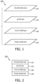
- FIGURES 1 and 2 schematically illustrate an example radiation detector 100 such as a pSi QD radiation detector.
- FIGURE 1 schematically illustrates an exploded perspective view of individual layers shown as planes
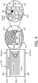
- FIGURE 2 schematically illustrates a front view with the individual layers shown as blocks.
- the relative shape, size, geometry, etc. of one or more of the layers therein is not limiting and may have other shape, size, geometry, etc. In general, in some instances the shape, size, geometry, etc. is based on the particular application.
- the detector includes more or less layers.
- one or more of the layers can be a Si and/or other layer.
- the illustrated pSi QD radiation detector 100 includes at least a QD photovoltaic layer 102, a pSi QD layer 104, an acquisition and communication (Acq & Comm) layer 106, and an energy storage layer 108.
- a non-limiting example of QD's and QD radiation detectors are described in patent application serial number EP 14186022.1, entitled “Encapsulated materials in porous particles,” and filed on September 23, 2014 , and patent application publication number WO 2017/025888 A1, entitled “Quantum Dot Based Imaging Detector,” and filed on August 8, 2016 .
- the QD photovoltaic layer 102 is configured to absorb certain radiation and generate photovoltaic charge in response thereto.
- the pSi QD layer 104 is configured to absorb certain radiation and generate an electrical signal indicative of the electrical energy of the absorbed radiation.
- QD's in holes in the porous Si interact with the Si to convert the radiation into the charge via electron-hole pair generation and separation.
- the acquisition and communication layer 106 is configured to measure the electrical signal and route data indicative thereof off the radiation detector.
- the energy storage layer 108 stores the photovoltaic charge and supplies the acquisition and communication layer 106 with operating power. The stored charge can also be used to supply power to other devices requiring power.
- the example radiation detector 100 can be encapsulated, e.g., with a light transparent coating, film, cover, etc.
- the pSi QD radiation detector 100 can be used individually (as shown) or with one or more other pSi QD radiation detectors 100 and/or other radiation detectors, e.g., in a module or otherwise.
- the pSi QD radiation detector is well-suited for applications such as unmanned ground or outer space applications and/or other applications where recharging the energy storage layer 108 is not feasible and the QS photovoltaic layer 102 produces enough charge for operating power. Other applications are also contemplated herein.
- the QD photovoltaic layer 102 is a top layer, with respect to the direction of incident radiation.
- the QD photovoltaic layer 102 is a bottom layer, i.e. below the energy storage layer 108.
- the QD photovoltaic layer 102 extends vertical relative to the pSi QD layer 104, the acquisition and communication layer 106 and energy storage layer 108, along a side (e.g., left, back, right, front) of one more of the pSi QD layer 104, the acquisition and communication layer 106 and energy storage layer 108.
- the radiation detector 100 includes multiple QD photovoltaic layers 102 on one or more sides (e.g., top, bottom, left, back, right, front) of the radiation detector 100, including a same side and/or different sides.
- the additional QD photovoltaic layers increase energy absorption.
- FIGURE 3 schematically illustrates a non-limiting example of the pSi QD radiation detector 100 of FIGURES 1 and 2 . It is to be understood that the size, shape, etc. is for explanatory purposes and is not limiting.
- the QD photovoltaic layer 102 includes a radiation translucent substrate 302, a QD absorbing photovoltaic material 304, an electrically conductive contact 306.
- the QD photovoltaic layer 102 is a thinner layer relative to the pSi QD layer 104.
- the QD photovoltaic layer 102 is configured to absorb radiation and, in response thereto, generate photovoltaic power.
- the illustrated QD photovoltaic layer 102 includes a matrix of QD's tuned to a specific band gap / segment of the light spectrum, e.g., the visible light segment, the infrared (IR) segment, and/or other segment. In one instance, the crystals are tuned through the dimension (e.g., size) of the QD's.
- Radiation 300 e.g., photons
- Radiation 300 is received by the radiation translucent substrate 302.
- QD photovoltaic layer An example of a QD photovoltaic layer is described in Bhandari, et al., "Thin film solar cells based on the heterojunction of colloidal PbS quantum dots with CdS," Solar Energy Materials & Solar Cells, Volume 117, October 2013, pages 476-482 .
- Another example is described in Nozik, et al., “Semiconductor Quantum Dots and Quantum Dot Arrays and Applications of Multiple Exciton Generation to Third-Generation Photovoltaic Solar Cells," Chemical Reviews, Volume 110, Revision 2010, pages 6873-6890 .
- Semonin, et al. “Quantum Dots for Next Generation Photovoltaics," Materials Today, Volume 15, November 2012, Issue 11 .
- Other configurations are also contemplated herein.
- the pSi QD layer 104 includes a pSi membrane 308 with bulk Si material 310 and columnar holes 312 filled with QD's 314 (lead sulfide (PbS) in this example).
- the pSi QD layer 104 is a thicker layer relative to the QD photovoltaic layer 102.
- the QD's 314 in the columnar holes 312 and the Si in the bulk Si material 310 interact to convert received radiation 300 into an electrical charge (signal, pulse, etc.) via electron-hole pair generation.
- An example of the pSi QD layer 104 is described in patent application serial number 62/649,615, entitled “Pixel Definition in a Porous Silicon Quantum Dot Radiation Detector,” filed March 29, 2018.
- the pSi QD layer 104 further includes electrical conductors (Aluminum (Al) contacts in this example) 402 and 404 on opposing sides 406 and 408 of the pSi membrane 308.
- electrical conductors Al
- Al aluminum
- the QD's 314 in the columnar holes 312 and the Si in the bulk Si material 310 interact to convert the received radiation 300 into an electrical charge via electron-hole pair generation
- the acquisition and communication layer 106 includes a metal layer 316, a substrate 318 and circuit 320.
- the metal layer 316 is electrically coupled to the bulk Si material 310 of the pSi QD layer 104 through an electrically conductive adhesive or the like.
- An example with pixelation is described in patent application serial number 62/649,615.
- the circuit 320 e.g., an application specific integrated circuit (ASIC) or the like
- ASIC application specific integrated circuit
- the signals generated in the pSi QD layer 104 are routed to the circuit 320 by way of through-hole vias (THVs) 319 (e.g., through Si vias) in the substrate 318.
- TSVs through-hole vias
- these signals are routed by way of wires, a flex circuit, or the like.
- the circuit 320 includes readout electronics (not visible) and reads out the measured signals.
- the circuit 320 first processes (e.g., amplify, filter, combine, etc.) the measured signals and then reads out the processed signals.
- the circuit 320 can be configured to control both data acquisition and data read out.
- the energy storage layer 108 includes a charge storage device 322 such as a rechargeable battery, a super capacitor, and/or the like.
- the charge generated in the QD photovoltaic layer 102 is routed to the energy storage layer 108 through an electrical conduit 324 such as wires, a flex circuit, or the like disposed at a side 326 of the pSi QD radiation detector 100.
- the charge stored in the energy storage layer 108 is routed to the acquisition and communication layer 106 by way of electrical contacts 328 and 330 on the charge storage device 322 and the ASIC 320.
- the charge is by way of wires, a flexible printed circuit board, and the like.
- the circuit 320 controls energy storage layer 108.
- the energy storage layer 108 includes its own circuit for control.
- a width 332 and a depth 333 of the pSi QD radiation detector 100 are in a range of twenty to fifty millimeters (20-50 mm), a thickness 334 of the radiation translucent substrate is approximately ten microns (10 ⁇ m), a thickness 336 of the combination of the QD absorbing photovoltaic material 304 and the electrically conductive contact 306 is approximately one hundred microns (100 ⁇ m), a thickness 338 of the pSi membrane is in a range of three hundred to one thousand microns (300-1000 ⁇ m), a thickness 340 of the acquisition and communication layer 106 is in a range of seven hundred to one thousand microns (700-1000 ⁇ m), and a thickness 342 of the energy storage layer 108 is in a range of a millimeter or larger (1+mm).
- the pSi QD radiation detector 100 with a different arrangement of layers and/or with layers with different thicknesses is also contemplated herein.
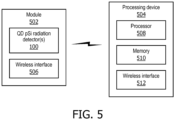
- FIGURE 5 illustrates an example radiation detection and processing system.
- the radiation detection and processing system includes a module 502 with one or more QD-pSi radiation detectors 100 and a processing device 504, which is remote from and part of the one or more QD-pSi radiation detectors.
- the one or more QD-pSi radiation detectors 100 are located at an unmanned ground location or in outer space. Generally, at these locations, manually recharging the energy storage device of the energy storage layer 104 is not feasible. However, for lower power application, the charge produced by the QD photovoltaic layer 102 and stored in the energy storage layer 104 provides operating power for the one or more QD-pSi radiation detectors to measure detected radiation and transmit that radiation to another device such as the processing device 504.
- the module 502 and/or the one or more QD-pSi radiation detectors 100 includes at least a wireless interface 506.
- the wireless interface 506 is configured with a wireless transmitter configured to transmit the data indicative of the measured signal to the processing device 504.
- the wireless interface 506 is configured with a wireless transceiver and not only transmits the data, but also receives data (e.g., a command, a request for data, etc.) from the processing device 504.
- the wireless interface 506 is also powered by the energy storage layer 108.
- the processing device 504 includes a processor 508 (e.g., a central processing unit (CPU), a microprocessor, etc.), a memory device (memory) 510, and a wireless interface 512.
- the memory device 510 includes one or more algorithms, such as one or more spectral and/or non-spectral algorithms, for processing the data received from the module 502. Such processing, in one example, includes generating an image.
- the processor 508 remains in a standby lower power mode to only send data when triggered by detected radiation, which can save power.
- the wireless interface 512 is configured with a complementary wireless receiver or wireless transceiver for receiving or receiving and transmitting data (e.g., a command, a request for data, etc.).
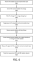
- FIGURE 6 illustrates an example method in accordance with an embodiment(s) herein.
- first radiation is received by the QD photovoltaic layer 102 of the pSi QD radiation detector 100.
- the QD photovoltaic layer 102 converts the received radiation into charge.
- the energy storage layer 108 of the pSi QD radiation detector 100 stores the charge.
- the acquisition and communication layer 106 of the pSi QD radiation detector 100 receives operating power from the energy storage layer 108.
- the pSi QD layer 104 of the pSi QD radiation detector 100 receives second radiation.
- the pSi QD layer 104 converts it into a signal indicative of an energy level of the second radiation.
- the acquisition and communication layer 106 measures the signal indicative of an energy level of the second radiation.
- the acquisition and communication layer 106 routes the (raw and/or processed) measurement off the pSi QD radiation detector 100.
- the routed (raw and/or processed) measurement is processed by a device remote from the pSi QD radiation detector 100.
- a computer program may be stored/distributed on a suitable medium, such as an optical storage medium or a solid-state medium supplied together with or as part of other hardware, but may also be distributed in other forms, such as via the Internet or other wired or wireless telecommunication systems. Any reference signs in the claims should not be construed as limiting the scope.
Landscapes
- Physics & Mathematics (AREA)
- Health & Medical Sciences (AREA)
- Life Sciences & Earth Sciences (AREA)
- General Physics & Mathematics (AREA)
- High Energy & Nuclear Physics (AREA)
- Molecular Biology (AREA)
- Spectroscopy & Molecular Physics (AREA)
- Measurement Of Radiation (AREA)
- Light Receiving Elements (AREA)
- Photovoltaic Devices (AREA)
- Photometry And Measurement Of Optical Pulse Characteristics (AREA)
Claims (15)
- Strahlungsdetektor (100) umfassend:
eine photovoltaische Schicht (102) mit einer ersten Seite und einer zweiten gegenüberliegenden Seite, wobei die photovoltaische Schicht konfiguriert ist, um auf der ersten Seite erste Strahlung zu absorbieren und elektrische Ladung zu erzeugen; eine poröse Silizium-Quantenpunktschicht (104), die aufn der zweiten Seite der photovoltaischen Schicht angeordnet und konfiguriert ist, um zweite Strahlung zu empfangen und die empfangene zweite Strahlung in ein elektrisches Signal umzuwandeln, das indikativ für ein Energieniveau der empfangenen zweiten Strahlung ist; eine Erfassungs- und Kommunikationsschicht (106), die angrenzend an die poröse Silizium-Quantenpunktschicht angeordnet ist und konfiguriert ist, um das elektrische Signal zu empfangen und das elektrische Signal an eine von dem Strahlungsdetektor entfernte Vorrichtung zu übertragen; und eine Energiespeicherschicht (108), die angrenzend an die Erfassungs- und Kommunikationsschicht angeordnet und konfiguriert ist, um die elektrische Ladung zu speichern und die gespeicherte elektrische Ladung als Betriebsenergie an die Erfassungs- und Kommunikationsschicht zuzuführen. - Strahlungsdetektor nach Anspruch 1, wobei die photovoltaische Schicht eine Quantenpunktschicht beinhaltet.
- Strahlungsdetektor nach einem der Ansprüche 1 bis 2, wobei die photovoltaische Schicht konfiguriert ist, um Strahlung in einem Band aus der Gruppe bestehend aus sichtbarem Licht und Infrarotlicht zu absorbieren.
- Strahlungsdetektor nach einem der Ansprüche 1 bis 3, wobei die photovoltaische Schicht eine Quantenpunkt-Solarzelle beinhaltet.
- Der Strahlungsdetektor nach einem der Ansprüche 1 bis 4, wobei die Energiespeicherschicht eine oder mehrere Zellen einer wiederaufladbaren Batterie beinhaltet.
- Strahlungsdetektor nach einem der Ansprüche 1 bis 5, wobei die Energiespeicherschicht einen Superkondensator beinhaltet.
- Strahlungserfassungs- und -verarbeitungssystem, umfassend:
ein unbemanntes Boden- oder Himmelsstrahlungserfassungsmodul (502), das einen Strahlungsdetektor nach Anspruch 1 beinhaltet, wobei die Erfassungs- und Kommunikationsschicht ferner konfiguriert ist, um das elektrische Signal zu messen und die Messung an das Detektionsmodul weiterzuleiten; und eine Verarbeitungsvorrichtung (504), die konfiguriert ist, um die Messung zu empfangen und zu verarbeiten, wobei die Verarbeitungsvorrichtung von dem unbemannten Boden- oder Himmelsstrahlungserfassungsmodul entfernt ist. - System nach Anspruch 7, wobei das Modul eine drahtlose Schnittstelle (506) beinhaltet, die konfiguriert ist, um die Messung zumindest drahtlos an die Verarbeitungsvorrichtung zu übertragen.
- System nach einem der Ansprüche 7 bis 8, wobei die Verarbeitungsvorrichtung eine drahtlose Schnittstelle (512) beinhaltet, die konfiguriert ist, um zumindest die Messung drahtlos von dem Modul zu empfangen.
- System nach einem der Ansprüche 7 bis 9, wobei die Verarbeitungsvorrichtung ferner Folgendes beinhaltet: einen Speicher (510), der konfiguriert ist, um Anweisungen zum Verarbeiten der Daten von dem Modul zu speichern; und einen Prozessor (508), der konfiguriert ist, um die Daten des Moduls mit den Anweisungen zu verarbeiten.
- System nach einem der Ansprüche 7 bis 10, wobei die photovoltaische Schicht eine Quantenpunktschicht-Solarzelle umfasst, wobei die photovoltaische Schicht eine erste Stärke und die poröse Silizium-Quantenpunktschicht eine zweite Stärke aufweist und die erste Stärke kleiner ist als die zweite Stärke.
- Verfahren zum Verwenden eines Strahlungsdetektors nach Anspruch 1, umfassend:
Empfangen, mit einer photovoltaischen Schicht des Strahlungsdetektors, einer ersten Strahlung; Umwandeln, mit der photovoltaischen Schicht, der empfangenen ersten Strahlung in elektrische Ladung; Speichern der elektrischen Ladung in einer Energiespeicherschicht des Strahlungsdetektors; Versorgen einer Erfassungs- und Kommunikationsschicht des Strahlungsdetektors mit der gespeicherten elektrischen Ladung; Absorbieren, mit einer porösen Silizium-Quantenpunktschicht, einer zweiten Strahlung und Erzeugen einer elektrischen Ladung, die indikativ für die absorbierte zweite Strahlung ist; Messen des von der porösen Silizium-Quantenpunktschicht erzeugten elektrischen Signals mit der Stromerfassungs- und Kommunikationsschicht des Strahlungsdetektors; und Übertragen, mit der Erfassungs- und Kommunikationsschicht, von Daten, die indikativ für das gemessene Signal des Strahlungsdetektors sind. - Verfahren nach Anspruch 12, ferner umfassend: Betreiben der Erfassungs- und Kommunikationsschicht in einem energiesparenden Standby-Modus; Empfangen von Strahlung mit dem Strahlungsdetektor; und Auslösen, als Reaktion auf ein Empfangen der Strahlung, der Erfassungs- und Kommunikationsschicht, um das gemessene Signal zu verarbeiten, wobei die Daten indikativ für das verarbeitete gemessene Signal sind.
- Verfahren nach einem der Ansprüche 12 bis 13, ferner umfassend:
Empfangen der übertragenen Daten durch eine von dem Strahlungsdetektor entfernte Verarbeitungsvorrichtung; und Verarbeiten der empfangenen Daten mit der entfernten Verarbeitungsvorrichtung. - Verfahren nach einem der Ansprüche 12 bis 14, wobei die Erfassungs- und Kommunikationsschicht Betriebsenergie nur von der Energiespeicherschicht erhält.
Applications Claiming Priority (2)
| Application Number | Priority Date | Filing Date | Title |
|---|---|---|---|
| US201862650315P | 2018-03-30 | 2018-03-30 | |
| PCT/EP2019/057660 WO2019185675A1 (en) | 2018-03-30 | 2019-03-27 | Quantum dot radiation detector module with self-sustaining power |
Publications (2)
| Publication Number | Publication Date |
|---|---|
| EP3776004A1 EP3776004A1 (de) | 2021-02-17 |
| EP3776004B1 true EP3776004B1 (de) | 2023-10-18 |
Family
ID=66041444
Family Applications (1)
| Application Number | Title | Priority Date | Filing Date |
|---|---|---|---|
| EP19715423.0A Active EP3776004B1 (de) | 2018-03-30 | 2019-03-27 | Auf quantenpunkte basierter strahlungsdetektor mit selbst-betriebener energiequelle |
Country Status (4)
| Country | Link |
|---|---|
| US (1) | US11656372B2 (de) |
| EP (1) | EP3776004B1 (de) |
| JP (1) | JP7330203B2 (de) |
| WO (1) | WO2019185675A1 (de) |
Families Citing this family (1)
| Publication number | Priority date | Publication date | Assignee | Title |
|---|---|---|---|---|
| CN117293208B (zh) * | 2023-09-07 | 2024-05-10 | 中国科学院重庆绿色智能技术研究院 | 基于硫化铅/硅复合结构的光电探测器及其制备方法 |
Family Cites Families (13)
| Publication number | Priority date | Publication date | Assignee | Title |
|---|---|---|---|---|
| ATE528803T1 (de) * | 2006-08-07 | 2011-10-15 | Univ Wake Forest | Herstellung von organischen verbundmaterialien |
| JP2008288346A (ja) | 2007-05-16 | 2008-11-27 | Hiroshima Univ | 半導体素子 |
| KR101650841B1 (ko) | 2010-04-27 | 2016-08-25 | 삼성전자주식회사 | 수직 구조의 비휘발성 메모리 소자 |
| KR101822500B1 (ko) | 2011-09-06 | 2018-01-29 | 삼성전자주식회사 | 양자점층 제조 방법 및 양자점층을 포함한 양자점 광전자소자 |
| US10088580B2 (en) | 2012-05-31 | 2018-10-02 | Minnesota Imaging And Engineering Llc | Detector systems for radiation imaging |
| US9417331B2 (en) | 2012-06-01 | 2016-08-16 | Landauer, Inc. | System for wireless, motion and position-sensing, integrating radiation sensor and energy harvester for occupational and environmental dosimetry |
| KR20150003393A (ko) | 2012-06-01 | 2015-01-08 | 랜다우어, 인크. | 직업적 및 환경적 선량계측을 위한 무선, 움직임 및 위치-감지, 집적형 방사선 센서 |
| RU134360U1 (ru) | 2012-11-07 | 2013-11-10 | Федеральное государственное бюджетное учреждение науки Институт общей физики им. А.М. Прохорова Российской академии наук (ИОФ РАН) | Фотовольтаический приемник ик излучения на квантовых точках |
| JP2014146701A (ja) | 2013-01-29 | 2014-08-14 | Kyocera Corp | 量子ドットおよび太陽電池 |
| EP3172622B1 (de) | 2014-07-21 | 2019-02-27 | Varex Imaging Corporation | Verfahren und system für differenzreferenzsignalverteilung |
| JP2016053534A (ja) | 2014-09-04 | 2016-04-14 | 国立大学法人大阪大学 | 放射性プルーム監視システムおよび放射性物質検出装置 |
| EP3197981A1 (de) | 2014-09-23 | 2017-08-02 | Philips Lighting Holding B.V. | Verkapselten materialien in porösen partikeln |
| US10527739B2 (en) | 2015-08-07 | 2020-01-07 | Koninklijke Philips N.V. | Quantum dot based imaging detector |
-
2019
- 2019-03-27 EP EP19715423.0A patent/EP3776004B1/de active Active
- 2019-03-27 US US17/042,258 patent/US11656372B2/en active Active
- 2019-03-27 WO PCT/EP2019/057660 patent/WO2019185675A1/en not_active Ceased
- 2019-03-27 JP JP2020552862A patent/JP7330203B2/ja active Active
Also Published As
| Publication number | Publication date |
|---|---|
| US20210141104A1 (en) | 2021-05-13 |
| JP2021523345A (ja) | 2021-09-02 |
| EP3776004A1 (de) | 2021-02-17 |
| RU2020135490A (ru) | 2022-05-04 |
| JP7330203B2 (ja) | 2023-08-21 |
| US11656372B2 (en) | 2023-05-23 |
| WO2019185675A1 (en) | 2019-10-03 |
Similar Documents
| Publication | Publication Date | Title |
|---|---|---|
| US11744090B2 (en) | Self-powered perovskite X-ray detector | |
| US7902976B2 (en) | Ionising radiation detector | |
| EP2494376B1 (de) | Detektor, verfahren zur herstellung eines detektors und bildgebungsgerät | |
| US10483316B2 (en) | Fabrication and operation of multi-function flexible radiation detection systems | |
| US8829460B2 (en) | Three-dimensional boron particle loaded thermal neutron detector | |
| US10083772B2 (en) | Aligned carbon nanotubes for improved X-ray detector performance | |
| US20130015363A1 (en) | Detector, method for manufacturing a detector and imaging apparatus | |
| CN101836129A (zh) | 盒式放射线图像固体检测器 | |
| CN101752391B (zh) | 具有mos全耗尽漂移通道的雪崩漂移探测器及其探测方法 | |
| CN112212855B (zh) | 一种应用于x射线脉冲星导航终端的轻小型探测器 | |
| US12404691B2 (en) | Solar energy conversion spherical dome | |
| US11656372B2 (en) | Quantum dot radiation detector module with self-sustaining power | |
| Carvalho et al. | CMOS indoor light energy harvesting system for wireless sensing applications | |
| WO2018195383A1 (en) | Two-dimensional material with electroactivity and photosensitivity | |
| RU2786152C2 (ru) | Модуль детектора излучения на квантовых точках с автономным питанием | |
| CN111522052B (zh) | 一种x光探测器结构及其工作方法 | |
| EP3655975A1 (de) | Nukleare mikrobatterie | |
| CN119936960B (zh) | 基于纳米镀层像素传感器的中子测量系统及方法 | |
| CN119916430B (zh) | 双cmos传感器与转换材料组合的中子测量系统 | |
| JP2021523345A5 (de) | ||
| Pinsky et al. | Development of a new active personal dosimeter for use in space radiation environments | |
| Caroli et al. | A three-dimensional CZT detector as a focal plane prototype for a Laue Lens telescope | |
| EP4300579A1 (de) | Integrierter plasmonischer energiesammler auf einem chip, mikrosuperkondensator und sensor sowie verfahren zur herstellung davon | |
| EP3776006B1 (de) | Pixeldefinierung in einem porösen silizium quantenpunkt strahlungsdetektor | |
| Labanti et al. | Array of X and gamma ray scintillator detector for space gamma ray telescope application |
Legal Events
| Date | Code | Title | Description |
|---|---|---|---|
| STAA | Information on the status of an ep patent application or granted ep patent |
Free format text: STATUS: UNKNOWN |
|
| STAA | Information on the status of an ep patent application or granted ep patent |
Free format text: STATUS: THE INTERNATIONAL PUBLICATION HAS BEEN MADE |
|
| PUAI | Public reference made under article 153(3) epc to a published international application that has entered the european phase |
Free format text: ORIGINAL CODE: 0009012 |
|
| STAA | Information on the status of an ep patent application or granted ep patent |
Free format text: STATUS: REQUEST FOR EXAMINATION WAS MADE |
|
| 17P | Request for examination filed |
Effective date: 20201030 |
|
| AK | Designated contracting states |
Kind code of ref document: A1 Designated state(s): AL AT BE BG CH CY CZ DE DK EE ES FI FR GB GR HR HU IE IS IT LI LT LU LV MC MK MT NL NO PL PT RO RS SE SI SK SM TR |
|
| AX | Request for extension of the european patent |
Extension state: BA ME |
|
| DAV | Request for validation of the european patent (deleted) | ||
| DAX | Request for extension of the european patent (deleted) | ||
| GRAP | Despatch of communication of intention to grant a patent |
Free format text: ORIGINAL CODE: EPIDOSNIGR1 |
|
| STAA | Information on the status of an ep patent application or granted ep patent |
Free format text: STATUS: GRANT OF PATENT IS INTENDED |
|
| INTG | Intention to grant announced |
Effective date: 20230510 |
|
| GRAS | Grant fee paid |
Free format text: ORIGINAL CODE: EPIDOSNIGR3 |
|
| GRAA | (expected) grant |
Free format text: ORIGINAL CODE: 0009210 |
|
| STAA | Information on the status of an ep patent application or granted ep patent |
Free format text: STATUS: THE PATENT HAS BEEN GRANTED |
|
| AK | Designated contracting states |
Kind code of ref document: B1 Designated state(s): AL AT BE BG CH CY CZ DE DK EE ES FI FR GB GR HR HU IE IS IT LI LT LU LV MC MK MT NL NO PL PT RO RS SE SI SK SM TR |
|
| REG | Reference to a national code |
Ref country code: GB Ref legal event code: FG4D |
|
| REG | Reference to a national code |
Ref country code: CH Ref legal event code: EP |
|
| REG | Reference to a national code |
Ref country code: IE Ref legal event code: FG4D |
|
| REG | Reference to a national code |
Ref country code: DE Ref legal event code: R096 Ref document number: 602019039555 Country of ref document: DE |
|
| REG | Reference to a national code |
Ref country code: DE Ref legal event code: R084 Ref document number: 602019039555 Country of ref document: DE |
|
| REG | Reference to a national code |
Ref country code: LT Ref legal event code: MG9D |
|
| REG | Reference to a national code |
Ref country code: NL Ref legal event code: MP Effective date: 20231018 |
|
| REG | Reference to a national code |
Ref country code: AT Ref legal event code: MK05 Ref document number: 1622924 Country of ref document: AT Kind code of ref document: T Effective date: 20231018 |
|
| PG25 | Lapsed in a contracting state [announced via postgrant information from national office to epo] |
Ref country code: NL Free format text: LAPSE BECAUSE OF FAILURE TO SUBMIT A TRANSLATION OF THE DESCRIPTION OR TO PAY THE FEE WITHIN THE PRESCRIBED TIME-LIMIT Effective date: 20231018 |
|
| PG25 | Lapsed in a contracting state [announced via postgrant information from national office to epo] |
Ref country code: GR Free format text: LAPSE BECAUSE OF FAILURE TO SUBMIT A TRANSLATION OF THE DESCRIPTION OR TO PAY THE FEE WITHIN THE PRESCRIBED TIME-LIMIT Effective date: 20240119 |
|
| PG25 | Lapsed in a contracting state [announced via postgrant information from national office to epo] |
Ref country code: IS Free format text: LAPSE BECAUSE OF FAILURE TO SUBMIT A TRANSLATION OF THE DESCRIPTION OR TO PAY THE FEE WITHIN THE PRESCRIBED TIME-LIMIT Effective date: 20240218 |
|
| REG | Reference to a national code |
Ref country code: GB Ref legal event code: 746 Effective date: 20240314 |
|
| PG25 | Lapsed in a contracting state [announced via postgrant information from national office to epo] |
Ref country code: LT Free format text: LAPSE BECAUSE OF FAILURE TO SUBMIT A TRANSLATION OF THE DESCRIPTION OR TO PAY THE FEE WITHIN THE PRESCRIBED TIME-LIMIT Effective date: 20231018 |
|
| PG25 | Lapsed in a contracting state [announced via postgrant information from national office to epo] |
Ref country code: AT Free format text: LAPSE BECAUSE OF FAILURE TO SUBMIT A TRANSLATION OF THE DESCRIPTION OR TO PAY THE FEE WITHIN THE PRESCRIBED TIME-LIMIT Effective date: 20231018 |
|
| PG25 | Lapsed in a contracting state [announced via postgrant information from national office to epo] |
Ref country code: ES Free format text: LAPSE BECAUSE OF FAILURE TO SUBMIT A TRANSLATION OF THE DESCRIPTION OR TO PAY THE FEE WITHIN THE PRESCRIBED TIME-LIMIT Effective date: 20231018 |
|
| PG25 | Lapsed in a contracting state [announced via postgrant information from national office to epo] |
Ref country code: LT Free format text: LAPSE BECAUSE OF FAILURE TO SUBMIT A TRANSLATION OF THE DESCRIPTION OR TO PAY THE FEE WITHIN THE PRESCRIBED TIME-LIMIT Effective date: 20231018 Ref country code: IS Free format text: LAPSE BECAUSE OF FAILURE TO SUBMIT A TRANSLATION OF THE DESCRIPTION OR TO PAY THE FEE WITHIN THE PRESCRIBED TIME-LIMIT Effective date: 20240218 Ref country code: GR Free format text: LAPSE BECAUSE OF FAILURE TO SUBMIT A TRANSLATION OF THE DESCRIPTION OR TO PAY THE FEE WITHIN THE PRESCRIBED TIME-LIMIT Effective date: 20240119 Ref country code: ES Free format text: LAPSE BECAUSE OF FAILURE TO SUBMIT A TRANSLATION OF THE DESCRIPTION OR TO PAY THE FEE WITHIN THE PRESCRIBED TIME-LIMIT Effective date: 20231018 Ref country code: BG Free format text: LAPSE BECAUSE OF FAILURE TO SUBMIT A TRANSLATION OF THE DESCRIPTION OR TO PAY THE FEE WITHIN THE PRESCRIBED TIME-LIMIT Effective date: 20240118 Ref country code: AT Free format text: LAPSE BECAUSE OF FAILURE TO SUBMIT A TRANSLATION OF THE DESCRIPTION OR TO PAY THE FEE WITHIN THE PRESCRIBED TIME-LIMIT Effective date: 20231018 Ref country code: PT Free format text: LAPSE BECAUSE OF FAILURE TO SUBMIT A TRANSLATION OF THE DESCRIPTION OR TO PAY THE FEE WITHIN THE PRESCRIBED TIME-LIMIT Effective date: 20240219 |
|
| PG25 | Lapsed in a contracting state [announced via postgrant information from national office to epo] |
Ref country code: SE Free format text: LAPSE BECAUSE OF FAILURE TO SUBMIT A TRANSLATION OF THE DESCRIPTION OR TO PAY THE FEE WITHIN THE PRESCRIBED TIME-LIMIT Effective date: 20231018 Ref country code: RS Free format text: LAPSE BECAUSE OF FAILURE TO SUBMIT A TRANSLATION OF THE DESCRIPTION OR TO PAY THE FEE WITHIN THE PRESCRIBED TIME-LIMIT Effective date: 20231018 Ref country code: PL Free format text: LAPSE BECAUSE OF FAILURE TO SUBMIT A TRANSLATION OF THE DESCRIPTION OR TO PAY THE FEE WITHIN THE PRESCRIBED TIME-LIMIT Effective date: 20231018 Ref country code: NO Free format text: LAPSE BECAUSE OF FAILURE TO SUBMIT A TRANSLATION OF THE DESCRIPTION OR TO PAY THE FEE WITHIN THE PRESCRIBED TIME-LIMIT Effective date: 20240118 Ref country code: LV Free format text: LAPSE BECAUSE OF FAILURE TO SUBMIT A TRANSLATION OF THE DESCRIPTION OR TO PAY THE FEE WITHIN THE PRESCRIBED TIME-LIMIT Effective date: 20231018 Ref country code: HR Free format text: LAPSE BECAUSE OF FAILURE TO SUBMIT A TRANSLATION OF THE DESCRIPTION OR TO PAY THE FEE WITHIN THE PRESCRIBED TIME-LIMIT Effective date: 20231018 |
|
| PG25 | Lapsed in a contracting state [announced via postgrant information from national office to epo] |
Ref country code: DK Free format text: LAPSE BECAUSE OF FAILURE TO SUBMIT A TRANSLATION OF THE DESCRIPTION OR TO PAY THE FEE WITHIN THE PRESCRIBED TIME-LIMIT Effective date: 20231018 |
|
| REG | Reference to a national code |
Ref country code: DE Ref legal event code: R097 Ref document number: 602019039555 Country of ref document: DE |
|
| PG25 | Lapsed in a contracting state [announced via postgrant information from national office to epo] |
Ref country code: CZ Free format text: LAPSE BECAUSE OF FAILURE TO SUBMIT A TRANSLATION OF THE DESCRIPTION OR TO PAY THE FEE WITHIN THE PRESCRIBED TIME-LIMIT Effective date: 20231018 |
|
| PG25 | Lapsed in a contracting state [announced via postgrant information from national office to epo] |
Ref country code: SK Free format text: LAPSE BECAUSE OF FAILURE TO SUBMIT A TRANSLATION OF THE DESCRIPTION OR TO PAY THE FEE WITHIN THE PRESCRIBED TIME-LIMIT Effective date: 20231018 |
|
| PG25 | Lapsed in a contracting state [announced via postgrant information from national office to epo] |
Ref country code: SM Free format text: LAPSE BECAUSE OF FAILURE TO SUBMIT A TRANSLATION OF THE DESCRIPTION OR TO PAY THE FEE WITHIN THE PRESCRIBED TIME-LIMIT Effective date: 20231018 Ref country code: SK Free format text: LAPSE BECAUSE OF FAILURE TO SUBMIT A TRANSLATION OF THE DESCRIPTION OR TO PAY THE FEE WITHIN THE PRESCRIBED TIME-LIMIT Effective date: 20231018 Ref country code: RO Free format text: LAPSE BECAUSE OF FAILURE TO SUBMIT A TRANSLATION OF THE DESCRIPTION OR TO PAY THE FEE WITHIN THE PRESCRIBED TIME-LIMIT Effective date: 20231018 Ref country code: IT Free format text: LAPSE BECAUSE OF FAILURE TO SUBMIT A TRANSLATION OF THE DESCRIPTION OR TO PAY THE FEE WITHIN THE PRESCRIBED TIME-LIMIT Effective date: 20231018 Ref country code: EE Free format text: LAPSE BECAUSE OF FAILURE TO SUBMIT A TRANSLATION OF THE DESCRIPTION OR TO PAY THE FEE WITHIN THE PRESCRIBED TIME-LIMIT Effective date: 20231018 Ref country code: DK Free format text: LAPSE BECAUSE OF FAILURE TO SUBMIT A TRANSLATION OF THE DESCRIPTION OR TO PAY THE FEE WITHIN THE PRESCRIBED TIME-LIMIT Effective date: 20231018 Ref country code: CZ Free format text: LAPSE BECAUSE OF FAILURE TO SUBMIT A TRANSLATION OF THE DESCRIPTION OR TO PAY THE FEE WITHIN THE PRESCRIBED TIME-LIMIT Effective date: 20231018 |
|
| PLBE | No opposition filed within time limit |
Free format text: ORIGINAL CODE: 0009261 |
|
| STAA | Information on the status of an ep patent application or granted ep patent |
Free format text: STATUS: NO OPPOSITION FILED WITHIN TIME LIMIT |
|
| 26N | No opposition filed |
Effective date: 20240719 |
|
| PG25 | Lapsed in a contracting state [announced via postgrant information from national office to epo] |
Ref country code: SI Free format text: LAPSE BECAUSE OF FAILURE TO SUBMIT A TRANSLATION OF THE DESCRIPTION OR TO PAY THE FEE WITHIN THE PRESCRIBED TIME-LIMIT Effective date: 20231018 |
|
| PG25 | Lapsed in a contracting state [announced via postgrant information from national office to epo] |
Ref country code: SI Free format text: LAPSE BECAUSE OF FAILURE TO SUBMIT A TRANSLATION OF THE DESCRIPTION OR TO PAY THE FEE WITHIN THE PRESCRIBED TIME-LIMIT Effective date: 20231018 |
|
| REG | Reference to a national code |
Ref country code: CH Ref legal event code: PL |
|
| PG25 | Lapsed in a contracting state [announced via postgrant information from national office to epo] |
Ref country code: LU Free format text: LAPSE BECAUSE OF NON-PAYMENT OF DUE FEES Effective date: 20240327 |
|
| PG25 | Lapsed in a contracting state [announced via postgrant information from national office to epo] |
Ref country code: MC Free format text: LAPSE BECAUSE OF FAILURE TO SUBMIT A TRANSLATION OF THE DESCRIPTION OR TO PAY THE FEE WITHIN THE PRESCRIBED TIME-LIMIT Effective date: 20231018 |
|
| PG25 | Lapsed in a contracting state [announced via postgrant information from national office to epo] |
Ref country code: MC Free format text: LAPSE BECAUSE OF FAILURE TO SUBMIT A TRANSLATION OF THE DESCRIPTION OR TO PAY THE FEE WITHIN THE PRESCRIBED TIME-LIMIT Effective date: 20231018 Ref country code: LU Free format text: LAPSE BECAUSE OF NON-PAYMENT OF DUE FEES Effective date: 20240327 |
|
| REG | Reference to a national code |
Ref country code: BE Ref legal event code: MM Effective date: 20240331 |
|
| PG25 | Lapsed in a contracting state [announced via postgrant information from national office to epo] |
Ref country code: BE Free format text: LAPSE BECAUSE OF NON-PAYMENT OF DUE FEES Effective date: 20240331 |
|
| PG25 | Lapsed in a contracting state [announced via postgrant information from national office to epo] |
Ref country code: FR Free format text: LAPSE BECAUSE OF NON-PAYMENT OF DUE FEES Effective date: 20240331 |
|
| PG25 | Lapsed in a contracting state [announced via postgrant information from national office to epo] |
Ref country code: IE Free format text: LAPSE BECAUSE OF NON-PAYMENT OF DUE FEES Effective date: 20240327 |
|
| PG25 | Lapsed in a contracting state [announced via postgrant information from national office to epo] |
Ref country code: IE Free format text: LAPSE BECAUSE OF NON-PAYMENT OF DUE FEES Effective date: 20240327 Ref country code: FR Free format text: LAPSE BECAUSE OF NON-PAYMENT OF DUE FEES Effective date: 20240331 Ref country code: BE Free format text: LAPSE BECAUSE OF NON-PAYMENT OF DUE FEES Effective date: 20240331 Ref country code: CH Free format text: LAPSE BECAUSE OF NON-PAYMENT OF DUE FEES Effective date: 20240331 |
|
| PG25 | Lapsed in a contracting state [announced via postgrant information from national office to epo] |
Ref country code: CY Free format text: LAPSE BECAUSE OF FAILURE TO SUBMIT A TRANSLATION OF THE DESCRIPTION OR TO PAY THE FEE WITHIN THE PRESCRIBED TIME-LIMIT; INVALID AB INITIO Effective date: 20190327 |
|
| PG25 | Lapsed in a contracting state [announced via postgrant information from national office to epo] |
Ref country code: HU Free format text: LAPSE BECAUSE OF FAILURE TO SUBMIT A TRANSLATION OF THE DESCRIPTION OR TO PAY THE FEE WITHIN THE PRESCRIBED TIME-LIMIT; INVALID AB INITIO Effective date: 20190327 |
|
| PG25 | Lapsed in a contracting state [announced via postgrant information from national office to epo] |
Ref country code: FI Free format text: LAPSE BECAUSE OF FAILURE TO SUBMIT A TRANSLATION OF THE DESCRIPTION OR TO PAY THE FEE WITHIN THE PRESCRIBED TIME-LIMIT Effective date: 20231019 |
|
| PG25 | Lapsed in a contracting state [announced via postgrant information from national office to epo] |
Ref country code: TR Free format text: LAPSE BECAUSE OF FAILURE TO SUBMIT A TRANSLATION OF THE DESCRIPTION OR TO PAY THE FEE WITHIN THE PRESCRIBED TIME-LIMIT Effective date: 20231018 |
|
| PGFP | Annual fee paid to national office [announced via postgrant information from national office to epo] |
Ref country code: GB Payment date: 20260319 Year of fee payment: 8 |
|
| PGFP | Annual fee paid to national office [announced via postgrant information from national office to epo] |
Ref country code: DE Payment date: 20260320 Year of fee payment: 8 |