EP3769873A1 - Insert et outil de coupe le comprenant - Google Patents
Insert et outil de coupe le comprenant Download PDFInfo
- Publication number
- EP3769873A1 EP3769873A1 EP19770367.1A EP19770367A EP3769873A1 EP 3769873 A1 EP3769873 A1 EP 3769873A1 EP 19770367 A EP19770367 A EP 19770367A EP 3769873 A1 EP3769873 A1 EP 3769873A1
- Authority
- EP
- European Patent Office
- Prior art keywords
- layer
- base
- insert
- thickness
- insert according
- Prior art date
- Legal status (The legal status is an assumption and is not a legal conclusion. Google has not performed a legal analysis and makes no representation as to the accuracy of the status listed.)
- Pending
Links
Images

Classifications
-
- C—CHEMISTRY; METALLURGY
- C23—COATING METALLIC MATERIAL; COATING MATERIAL WITH METALLIC MATERIAL; CHEMICAL SURFACE TREATMENT; DIFFUSION TREATMENT OF METALLIC MATERIAL; COATING BY VACUUM EVAPORATION, BY SPUTTERING, BY ION IMPLANTATION OR BY CHEMICAL VAPOUR DEPOSITION, IN GENERAL; INHIBITING CORROSION OF METALLIC MATERIAL OR INCRUSTATION IN GENERAL
- C23C—COATING METALLIC MATERIAL; COATING MATERIAL WITH METALLIC MATERIAL; SURFACE TREATMENT OF METALLIC MATERIAL BY DIFFUSION INTO THE SURFACE, BY CHEMICAL CONVERSION OR SUBSTITUTION; COATING BY VACUUM EVAPORATION, BY SPUTTERING, BY ION IMPLANTATION OR BY CHEMICAL VAPOUR DEPOSITION, IN GENERAL
- C23C16/00—Chemical coating by decomposition of gaseous compounds, without leaving reaction products of surface material in the coating, i.e. chemical vapour deposition [CVD] processes
- C23C16/02—Pretreatment of the material to be coated
- C23C16/0272—Deposition of sub-layers, e.g. to promote the adhesion of the main coating
- C23C16/029—Graded interfaces
-
- C—CHEMISTRY; METALLURGY
- C22—METALLURGY; FERROUS OR NON-FERROUS ALLOYS; TREATMENT OF ALLOYS OR NON-FERROUS METALS
- C22C—ALLOYS
- C22C29/00—Alloys based on carbides, oxides, nitrides, borides, or silicides, e.g. cermets, or other metal compounds, e.g. oxynitrides, sulfides
- C22C29/005—Alloys based on carbides, oxides, nitrides, borides, or silicides, e.g. cermets, or other metal compounds, e.g. oxynitrides, sulfides comprising a particular metallic binder
-
- C—CHEMISTRY; METALLURGY
- C22—METALLURGY; FERROUS OR NON-FERROUS ALLOYS; TREATMENT OF ALLOYS OR NON-FERROUS METALS
- C22C—ALLOYS
- C22C29/00—Alloys based on carbides, oxides, nitrides, borides, or silicides, e.g. cermets, or other metal compounds, e.g. oxynitrides, sulfides
- C22C29/02—Alloys based on carbides, oxides, nitrides, borides, or silicides, e.g. cermets, or other metal compounds, e.g. oxynitrides, sulfides based on carbides or carbonitrides
- C22C29/04—Alloys based on carbides, oxides, nitrides, borides, or silicides, e.g. cermets, or other metal compounds, e.g. oxynitrides, sulfides based on carbides or carbonitrides based on carbonitrides
-
- C—CHEMISTRY; METALLURGY
- C23—COATING METALLIC MATERIAL; COATING MATERIAL WITH METALLIC MATERIAL; CHEMICAL SURFACE TREATMENT; DIFFUSION TREATMENT OF METALLIC MATERIAL; COATING BY VACUUM EVAPORATION, BY SPUTTERING, BY ION IMPLANTATION OR BY CHEMICAL VAPOUR DEPOSITION, IN GENERAL; INHIBITING CORROSION OF METALLIC MATERIAL OR INCRUSTATION IN GENERAL
- C23C—COATING METALLIC MATERIAL; COATING MATERIAL WITH METALLIC MATERIAL; SURFACE TREATMENT OF METALLIC MATERIAL BY DIFFUSION INTO THE SURFACE, BY CHEMICAL CONVERSION OR SUBSTITUTION; COATING BY VACUUM EVAPORATION, BY SPUTTERING, BY ION IMPLANTATION OR BY CHEMICAL VAPOUR DEPOSITION, IN GENERAL
- C23C16/00—Chemical coating by decomposition of gaseous compounds, without leaving reaction products of surface material in the coating, i.e. chemical vapour deposition [CVD] processes
- C23C16/22—Chemical coating by decomposition of gaseous compounds, without leaving reaction products of surface material in the coating, i.e. chemical vapour deposition [CVD] processes characterised by the deposition of inorganic material, other than metallic material
- C23C16/30—Deposition of compounds, mixtures or solid solutions, e.g. borides, carbides, nitrides
- C23C16/34—Nitrides
-
- C—CHEMISTRY; METALLURGY
- C23—COATING METALLIC MATERIAL; COATING MATERIAL WITH METALLIC MATERIAL; CHEMICAL SURFACE TREATMENT; DIFFUSION TREATMENT OF METALLIC MATERIAL; COATING BY VACUUM EVAPORATION, BY SPUTTERING, BY ION IMPLANTATION OR BY CHEMICAL VAPOUR DEPOSITION, IN GENERAL; INHIBITING CORROSION OF METALLIC MATERIAL OR INCRUSTATION IN GENERAL
- C23C—COATING METALLIC MATERIAL; COATING MATERIAL WITH METALLIC MATERIAL; SURFACE TREATMENT OF METALLIC MATERIAL BY DIFFUSION INTO THE SURFACE, BY CHEMICAL CONVERSION OR SUBSTITUTION; COATING BY VACUUM EVAPORATION, BY SPUTTERING, BY ION IMPLANTATION OR BY CHEMICAL VAPOUR DEPOSITION, IN GENERAL
- C23C16/00—Chemical coating by decomposition of gaseous compounds, without leaving reaction products of surface material in the coating, i.e. chemical vapour deposition [CVD] processes
- C23C16/22—Chemical coating by decomposition of gaseous compounds, without leaving reaction products of surface material in the coating, i.e. chemical vapour deposition [CVD] processes characterised by the deposition of inorganic material, other than metallic material
- C23C16/30—Deposition of compounds, mixtures or solid solutions, e.g. borides, carbides, nitrides
- C23C16/36—Carbonitrides
-
- C—CHEMISTRY; METALLURGY
- C23—COATING METALLIC MATERIAL; COATING MATERIAL WITH METALLIC MATERIAL; CHEMICAL SURFACE TREATMENT; DIFFUSION TREATMENT OF METALLIC MATERIAL; COATING BY VACUUM EVAPORATION, BY SPUTTERING, BY ION IMPLANTATION OR BY CHEMICAL VAPOUR DEPOSITION, IN GENERAL; INHIBITING CORROSION OF METALLIC MATERIAL OR INCRUSTATION IN GENERAL
- C23C—COATING METALLIC MATERIAL; COATING MATERIAL WITH METALLIC MATERIAL; SURFACE TREATMENT OF METALLIC MATERIAL BY DIFFUSION INTO THE SURFACE, BY CHEMICAL CONVERSION OR SUBSTITUTION; COATING BY VACUUM EVAPORATION, BY SPUTTERING, BY ION IMPLANTATION OR BY CHEMICAL VAPOUR DEPOSITION, IN GENERAL
- C23C28/00—Coating for obtaining at least two superposed coatings either by methods not provided for in a single one of groups C23C2/00 - C23C26/00 or by combinations of methods provided for in subclasses C23C and C25C or C25D
- C23C28/04—Coating for obtaining at least two superposed coatings either by methods not provided for in a single one of groups C23C2/00 - C23C26/00 or by combinations of methods provided for in subclasses C23C and C25C or C25D only coatings of inorganic non-metallic material
- C23C28/042—Coating for obtaining at least two superposed coatings either by methods not provided for in a single one of groups C23C2/00 - C23C26/00 or by combinations of methods provided for in subclasses C23C and C25C or C25D only coatings of inorganic non-metallic material including a refractory ceramic layer, e.g. refractory metal oxides, ZrO2, rare earth oxides
-
- C—CHEMISTRY; METALLURGY
- C23—COATING METALLIC MATERIAL; COATING MATERIAL WITH METALLIC MATERIAL; CHEMICAL SURFACE TREATMENT; DIFFUSION TREATMENT OF METALLIC MATERIAL; COATING BY VACUUM EVAPORATION, BY SPUTTERING, BY ION IMPLANTATION OR BY CHEMICAL VAPOUR DEPOSITION, IN GENERAL; INHIBITING CORROSION OF METALLIC MATERIAL OR INCRUSTATION IN GENERAL
- C23C—COATING METALLIC MATERIAL; COATING MATERIAL WITH METALLIC MATERIAL; SURFACE TREATMENT OF METALLIC MATERIAL BY DIFFUSION INTO THE SURFACE, BY CHEMICAL CONVERSION OR SUBSTITUTION; COATING BY VACUUM EVAPORATION, BY SPUTTERING, BY ION IMPLANTATION OR BY CHEMICAL VAPOUR DEPOSITION, IN GENERAL
- C23C28/00—Coating for obtaining at least two superposed coatings either by methods not provided for in a single one of groups C23C2/00 - C23C26/00 or by combinations of methods provided for in subclasses C23C and C25C or C25D
- C23C28/04—Coating for obtaining at least two superposed coatings either by methods not provided for in a single one of groups C23C2/00 - C23C26/00 or by combinations of methods provided for in subclasses C23C and C25C or C25D only coatings of inorganic non-metallic material
- C23C28/044—Coating for obtaining at least two superposed coatings either by methods not provided for in a single one of groups C23C2/00 - C23C26/00 or by combinations of methods provided for in subclasses C23C and C25C or C25D only coatings of inorganic non-metallic material coatings specially adapted for cutting tools or wear applications
-
- C—CHEMISTRY; METALLURGY
- C23—COATING METALLIC MATERIAL; COATING MATERIAL WITH METALLIC MATERIAL; CHEMICAL SURFACE TREATMENT; DIFFUSION TREATMENT OF METALLIC MATERIAL; COATING BY VACUUM EVAPORATION, BY SPUTTERING, BY ION IMPLANTATION OR BY CHEMICAL VAPOUR DEPOSITION, IN GENERAL; INHIBITING CORROSION OF METALLIC MATERIAL OR INCRUSTATION IN GENERAL
- C23C—COATING METALLIC MATERIAL; COATING MATERIAL WITH METALLIC MATERIAL; SURFACE TREATMENT OF METALLIC MATERIAL BY DIFFUSION INTO THE SURFACE, BY CHEMICAL CONVERSION OR SUBSTITUTION; COATING BY VACUUM EVAPORATION, BY SPUTTERING, BY ION IMPLANTATION OR BY CHEMICAL VAPOUR DEPOSITION, IN GENERAL
- C23C30/00—Coating with metallic material characterised only by the composition of the metallic material, i.e. not characterised by the coating process
- C23C30/005—Coating with metallic material characterised only by the composition of the metallic material, i.e. not characterised by the coating process on hard metal substrates
Definitions
- the present disclosure relates to an insert for use in a cutting process and a cutting tool including the same.
- Cermets including titanium (Ti) as a main component are now widely used as bases of members requiring wear resistance, sliding property, and chipping resistance, such as cutting tools, wear-resistant members, and sliding members.
- Patent Literature 1 discloses a surface-coated titanium carbonitride-based cermet cutting tool, in which a binder phase component based on cobalt (Co) and nickel (Ni) is contained, an erosion alloy phase composed of a metal binder phase component is formed on a surface portion, and a TiN layer having a diffusion-preventing effect is additionally provided thereon to suppress fracture or chipping.
- Patent Literature 1 Japanese Patent No. 5989930 Summary
- An insert of the present disclosure includes a base and a coating layer covering a surface of the base.
- the base includes a hard phase containing a carbonitride including Ti, and a binder phase containing Co.
- a CTiW compound that contains C, Ti, and W and satisfies a relation of C > Ti > W is positioned between the base and the coating layer.
- a cutting tool of the present disclosure includes a holder extending from a first end to a second end and having a pocket on the first end side, and the insert positioned in the pocket.
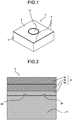
- an insert 1 of the present disclosure includes a base 3.
- the insert 1 of the present disclosure includes a coating layer 5 covering at least a part of the base 3.
- the insert 1 of the present disclosure has, for example, a quadrangular plate shape, and its upper surface in FIG. 1 is a rake face.
- the insert 1 has a lower surface on the side opposite to the upper surface and a side surface between the upper surface and the lower surface to connect to each of the upper and lower surfaces. At least a part of the side surface is a flank face.
- the insert 1 of the present disclosure has a cutting edge 7 positioned at at least a part of a ridge line where the upper surface and the side surface meet.
- the insert 1 has the cutting edge 7 positioned at at least a part of a ridge line where the rake face and the flank face meet.
- the insert 1 In the insert 1, the entire outer perimeter of the rake face may serve as the cutting edge 7.
- the insert 1 is not limited to such a configuration and, for example, may have the cutting edge 7 at only one side, or partially, of the quadrangular rake face.
- the size of the insert 1 is not limited and, for example, the length of one side of the rake face is set to about 3 to 20 mm.
- the thickness of the insert 1 is set, for example, to about 1 to 20 mm.
- the base 3 of the insert 1 of the present disclosure is composed of a cermet containing a hard phase containing a carbonitride including Ti and a binder phase containing Co.
- the cermet is a TiCN-based cermet.
- examples of the cermet include, but are not limited to, those containing TiC or TiN, etc. in addition to TiCN.
- the insert 1 of the present disclosure includes the coating layer 5 on the base 3. Since the insert 1 includes the coating layer 5 in this way, the wear resistance of the insert 1 is high.
- the coating layer 5 may be formed by a CVD process or a PVD process.
- a first layer 5a including a plurality of TiN particles, a second layer 5b including a plurality of TiCN particles, and a third layer 5c including a plurality of Al 2 O 3 particles may be disposed in this order from the side close to the base 3.
- a CTiW compound 25 containing C, Ti, and W and whose content in atm% satisfies the relation of C > Ti > W is positioned between the base 3 and the coating layer 5.
- the CTiW compound 25 may contain a total of 80 atm% or more of C, Ti, and W and contain 58 to 80 atm% of C, 7 to 25 atm% of Ti, and 1 to 15 atm% of W.
- the insert 1 of the present disclosure having the CTiW compound 25 described above is excellent in wear resistance and chipping resistance.
- the base may contain Co 0.93 W 0.07 .
- Co 0.93 W 0.07 is a crystal represented in PDF:01-071-7509 of the JCPDS card.
- the proportion of the Co 0.93 W 0.07 in all the crystals may be 5 to 10 in a crystalline phase analysis by X-ray diffraction.
- the proportion of Co 0.93 W 0.07 may be 8 to 10.
- the proportion of the Co 0.93 W 0.07 above is obtained by calculating the proportion of Co 0.93 W 0.07 in the proportions of all the crystals detected by Rietveld refinement using an X ray system manufactured by PANalytical, X'Pert Pro 2 ⁇ : 10 to 100, and analysis software RIETAN-FP.
- the Co content in the total amount of the binder phase may be 99.0 mass% or more.
- the Co content may be 99.5 mass% or more.
- Fe, Ni, and the like may be included as the binder phase, in addition to Co.
- the Co content (mass%) is a value obtained by measuring the masses of Co, Fe, and Ni included in the insert, dividing the mass of Co by the total mass, and multiplying by 100. In other words, the total amount of Fe and Ni in the binder phase included in the insert 1 of the present disclosure may be less than 1 mass%.
- the binder phase is Co alone, for example, the mean particle size as a raw material powder of the hard phase may be 1 ⁇ m or less, further 0.6 ⁇ m or less.
- the Co content in the base 3 may be 16 mass% or more.
- the width of TiN particles in a direction parallel to the surface of the base 3 (hereinafter also referred to as the width of TiN particles) of the first layer 5a may be 25 nm.
- the adhesion between the first layer 5a and the base 3 is excellent.
- the adhesion between the first layer 5a and the CTiW compound 25 is excellent.
- the coating film 5 is excellent in wear resistance.
- the width of TiN particles may be measured at a position 0.05 ⁇ m from the surface of the base 3.
- the width of TiN particles may be measured at a position 0.05 ⁇ m from the surface of the first compound 21.
- the width of TiN particles may be measured at a position half the thickness of the first layer 5a.
- the width of TiN particles is the mean value of the widths of 20 TiN particles measured at the position described above.
- the ratio (which hereinafter may be referred to as aspect ratio) of the height of TiN particles in a direction vertical to the surface of the base to the width of TiN particles in a direction parallel to the surface of the base 3 may be in a range of 1.0 to 1.7. With such a configuration, the adhesion force between the first layer 5a and the base 3 is excellent.
- the aspect ratio of TiN particles may be measured from TiN particles present at a position up to 0.05 ⁇ m from the surface of the base 3.
- the aspect ratio is the mean value of 20 TiN particles.
- the thickness of the first layer 5a may be 0.1 to 1.0 ⁇ m.
- the thickness of the first layer 5a is 0.1 ⁇ m or more, diffusion of the binder phase component included in the base 3 to the coating is suppressed, and the chipping resistance is excellent.
- the thickness of the first layer 5a is 1.0 ⁇ m or less, the TiCN particles included in the upper layer, that is, the second layer 5b are finer, and the wear resistance is excellent.
- the thickness of the first layer 5a may be 0.3 to 0.7 ⁇ m.
- the insert 1 includes the first layer 5a on the base 3.
- the insert 1 includes the second layer 5b on the first layer 5a.
- the TiCN layer 5b includes TiCN particles that are TiCN crystals.
- the base 3 may have a thermal expansion coefficient at 25 to 1000°C of 9.0 ⁇ 10 -6 /°C or more.
- the thermal expansion coefficient of the TiCN crystals is about 8 ⁇ 10 -6 /°C, and when the thermal expansion coefficient of the base 3 is 9.0 ⁇ 10 -6 /°C or more, the thermal expansion coefficient of the second layer 5b is smaller than the thermal expansion coefficient of the base 3.
- the second layer 5b is interposed between the base 3 and the first layer 5c to suppress peeling of the first layer 5c and suppress abrasive wear.
- the third layer 5c includes Al 2 O 3 particles that are Al 2 O 3 crystals.
- the thermal expansion coefficient of the Al 2 O 3 crystals is about 7.2 ⁇ 10 -6 /°C and is smaller than the thermal expansion coefficients of the base 3 and the second layer 5b.
- the base 3 and the second layer 5b may be in direct contact or, for example, the first layer 5a may be positioned between them as in the example in FIG. 2 .
- the first layer 5a is not necessarily composed of pure TiN particles and may contain, for example, O and/ or C.
- the second layer 5b and the third layer 5c may be in direct contact or, for example, a TiN layer (not illustrated) may be positioned between them.
- an adequate compressive stress can be exerted on the second layer 5b and the third layer 5c by adjusting the thermal expansion coefficient of the base 3 and the thickness of the third layer 5c.
- the thickness of the third layer 5c is 2 ⁇ m or more.
- the compressive stress exerted on the second layer 5b may be 250 to 500 MPa
- the compressive stress exerted on the third layer 5c may be 450 MPa or more
- the value of the compressive stress exerted on the third layer 5c may be larger than the compressive stress exerted on the second layer 5b.
- the insert 1 having such a configuration is excellent in wear resistance and durability.
- the compressive stresses exerted on the second layer 5b and the third layer 5c may be determined based on measurement using a 2D process. Specifically, a section of the flank face, 1 mm or more away from the cutting edge 7, is set as a measurement location, and X-ray diffraction peaks are measured. For the crystal structure specified from the measurement result, the compressive stress can be obtained by determining how the value of 2 ⁇ in the measurement result deviates from the value of 2 ⁇ serving as a standard described in the JCPDS card.
- the residual stress When a residual stress has a negative value, the residual stress is compressive stress. When the value of compressive stress is expressed, it is represented by an absolute value with no minus sign.
- the third layer 5c is at a position more distant from the base 3.
- the third layer 5c comes into contact with the workpiece before the second layer 5b.
- the third layer 5c includes Al 2 O 3 particles and has a thickness of 2 ⁇ m or more, the wear resistance and the oxidation resistance are high.
- the thickness of the third layer 5c may be 2.5 ⁇ m or more and 8.0 ⁇ m or less.
- the insert 1 having such a configuration is more excellent in wear resistance and oxidation resistance.
- the sum of the thickness of the second layer 5b and the thickness of the third layer 5c may be 7 ⁇ m or more and 18 ⁇ m or less.
- the sum of the thicknesses may be 8 ⁇ m or more and 16 ⁇ m or less.
- the second layer 5b may have a thickness of 5 ⁇ m or more and 10 ⁇ m or less. With such a range, the wear resistance and the chipping resistance of the insert 1 are excellent.
- the thickness of the third layer 5c may be 0.2 to 0.4 times the sum of the thickness of the second layer 5b and the thickness of the third layer 5c.
- the insert 1 having such a configuration is excellent in wear resistance and chipping resistance.
- the C axis of the Al 2 O 3 crystals of the third layer 5c may be oriented along a direction vertical to a main surface of the base 3.
- the third layer 5c may contain ⁇ -Al 2 O 3 crystals, and the ⁇ -Al 2 O 3 crystals may be shaped like a column extending in the vertical direction relative to the main surface of the base 3.
- a binder phase-enriched layer may be present on the surface, which has a higher proportion of the binder phase compared with the inside of the base 3.
- the thickness of the binder phase-enriched layer may be 1 ⁇ m or more and 10 ⁇ m or less.
- Table 1 illustrates the proportions of raw material powders to form the base of the insert used in Examples described later.
- the mean particle size of each raw material is 1 ⁇ m or less. These raw material powders are those typically used in production of cermets.
- the insert of the present disclosure can be obtained by controlling the composition of the base and the production condition of the coating layer.
- the coating film may be formed by a CVD process.
- the amount of C contained is adjusted to obtain the base containing CO 0.93 W 0.07 .
- the amount of C in the raw materials includes, for example, C included in the raw material powders, in addition to C added as carbon.
- the hard phase refers to the one that may be present as a hard phase in the insert and does not include, for example, metals, oxides, or carbonates of Fe, Ni, Co, Mn, and/or Mo.
- the powder After a binder is added to the raw material power having such a composition range, for example, the powder is formed into a desired shape by press molding and subjected to a debindering step for removing the binder component, and thereafter fired in a nitrogen or vacuum atmosphere in a temperature range of 1500 to 1550°C to produce a highly dense base.
- the product is held in a vacuum at 200°C and 300°C each for 1 hour, and then the temperature is increased to 450°C and held for 1 hour.
- CO 2 gas is introduced into a debindering furnace at a pressure of 1 to 5 kPa. In this way, the amount of C can be precisely controlled.
- the base may have a thermal expansion coefficient at 25 to 1000°C of 9.0 ⁇ 10 -6 /°C or more.
- a coating layer is provided.
- a first layer is formed on a surface of the base.
- a second layer is further formed on the first layer.
- a third layer is further formed thereon.
- the first layer, the second layer, and the third layer may be formed by a chemical vapor deposition (CVD) process.
- CVD chemical vapor deposition
- the higher the deposition temperature is in depositing a film the greater the compressive stress is exerted on the deposited film.
- the deposition temperature is then adjusted, if necessary.
- the ratio of Co in the binder phase components included in the base may be set to 99.0 mass% or more.
- the TiCl 4 concentration in the deposition condition for forming the first layer on the base may be set to 1.0 mol%.
- the proportion of Co in the binder phase included in the base may be set to 97.0 mass% or more, and the amount of Co included in the base may be set to 10 mass% or more.
- the first layer may be deposited, for example, at a temperature of 800 to 900°C, a pressure of 8 to 20 kPa, a TiCl 4 concentration of 1.0 to 2.5 mol%, a N 2 concentration of 25.0 to 49.9 mol%, and a H 2 concentration of 40.0 to 74.8 mol%.
- the CTiW compound prepared in advance may be attached to the surface of the base as desired, and thereafter a coating film may be formed to obtain the insert of the present disclosure.
- a cutting tool 101 of the present disclosure is, for example, a rod-shaped body extending from a first end (the upper end in FIG. 3 ) to a second end (the lower end in FIG. 3 ).
- the cutting tool 101 includes a holder 105 having a pocket 103 on the first end side (tip end side) and the aforementioned insert 1 positioned in the pocket 103. Because of the provision of the insert 1, the cutting tool 101 can perform a stable cutting process over a long time period.
- the pocket 103 is a portion to which the insert 1 is attached and has a seat surface parallel to a lower surface of the holder 105 and a constraint side surface inclined relative to the seat surface.
- the pocket 103 is open on the first end side of the holder 105.
- the insert 1 is positioned in the pocket 103.
- the lower surface of the insert 1 may be in direct contact with the pocket 103, or a sheet (not illustrated) may be sandwiched between the insert 1 and the pocket 103.
- the insert 1 is attached to the holder 105 such that at least a part of a section used as the cutting edge 7 at the ridge line on which the flank face and the rake face meet protrudes outward from the holder 105.
- the insert 1 is attached to the holder 105 by a fixing screw 107. That is, the insert 1 is attached to the holder 105 by inserting the fixing screw 107 into a through hole 17 of the insert 1, inserting the tip end of the fixing screw 107 into a screw hole (not illustrated) formed in the pocket 103, and screwing the screw portions together.
- steel and cast iron can be used as the material of the holder 105.
- steel with a high toughness may be used.
- the cutting tool 101 for use in a turning process is illustrated by way of example.
- the turning process include, but are not limited to, a boring process, an external process, a grooving process, and a facing process.
- the cutting tool 101 is not limited to the one for use in the turning process.
- the insert 1 in the embodiments may be used for the cutting tool 101 for use in a milling process.
- the base was produced as follows. A molded product in the shape of a tool was produced using raw material powders in proportions indicated in Table 1, and a binder component was removed, followed by firing to produce a base. Among these samples, the bases of Sample Nos. 1 to 14 are a cermet. The base of Sample No. 15 is a superalloy. At the debindering step, the product was held in a vacuum at 200°C and 300°C each for 1 hour, and then the temperature was increased to 450°C and held for 1 hour. At the step at 450°C, CO 2 gas was introduced at a pressure of 3 kPa into a debindering furnace.
- the first layer was formed under the deposition condition illustrated in Table 2 by a CVD process.
- the second layer was further formed on the first layer.
- the third layer was further formed on the second layer.
- Sample Nos. 4, 5, and 8 in which the TiCl 4 concentration is 1.0 mol% or more in the deposition condition for the first layer have the CTiW compound between the base and the coating film.
- the CTiW compound contains a total of 80 atm% or more of C, Ti, and W and contains 58 to 80 atm% of C, 7 to 25 atm% of Ti, and 1 to 15 atm% of W.
- the resulting insert underwent a cutting test under the following conditions.
- the samples having the CTiW compound exhibit excellent wear resistance and chipping resistance.
Landscapes
- Chemical & Material Sciences (AREA)
- Engineering & Computer Science (AREA)
- Materials Engineering (AREA)
- Mechanical Engineering (AREA)
- Metallurgy (AREA)
- Organic Chemistry (AREA)
- Chemical Kinetics & Catalysis (AREA)
- Inorganic Chemistry (AREA)
- General Chemical & Material Sciences (AREA)
- Ceramic Engineering (AREA)
- Chemical Vapour Deposition (AREA)
- Cutting Tools, Boring Holders, And Turrets (AREA)
Applications Claiming Priority (3)
| Application Number | Priority Date | Filing Date | Title |
|---|---|---|---|
| JP2018052842 | 2018-03-20 | ||
| JP2018223530 | 2018-11-29 | ||
| PCT/JP2019/010877 WO2019181792A1 (fr) | 2018-03-20 | 2019-03-15 | Insert et outil de coupe le comprenant |
Publications (2)
| Publication Number | Publication Date |
|---|---|
| EP3769873A1 true EP3769873A1 (fr) | 2021-01-27 |
| EP3769873A4 EP3769873A4 (fr) | 2021-12-01 |
Family
ID=67987310
Family Applications (1)
| Application Number | Title | Priority Date | Filing Date |
|---|---|---|---|
| EP19770367.1A Pending EP3769873A4 (fr) | 2018-03-20 | 2019-03-15 | Insert et outil de coupe le comprenant |
Country Status (4)
| Country | Link |
|---|---|
| EP (1) | EP3769873A4 (fr) |
| JP (1) | JP7057418B2 (fr) |
| CN (1) | CN111886098B (fr) |
| WO (1) | WO2019181792A1 (fr) |
Family Cites Families (17)
| Publication number | Priority date | Publication date | Assignee | Title |
|---|---|---|---|---|
| JPH07224346A (ja) * | 1994-02-10 | 1995-08-22 | Mitsubishi Materials Corp | 靭性のすぐれた炭窒化チタン系サーメット |
| US6413628B1 (en) * | 1994-05-12 | 2002-07-02 | Valenite Inc. | Titanium carbonitride coated cemented carbide and cutting inserts made from the same |
| US5920760A (en) * | 1994-05-31 | 1999-07-06 | Mitsubishi Materials Corporation | Coated hard alloy blade member |
| SE9502687D0 (sv) * | 1995-07-24 | 1995-07-24 | Sandvik Ab | CVD coated titanium based carbonitride cutting tool insert |
| JP4069749B2 (ja) * | 2003-01-24 | 2008-04-02 | 京セラ株式会社 | 荒加工用切削工具 |
| KR101168464B1 (ko) * | 2004-12-14 | 2012-07-26 | 스미또모 덴꼬오 하드메탈 가부시끼가이샤 | 표면 피복 절삭 공구 |
| JP4711714B2 (ja) * | 2005-03-30 | 2011-06-29 | 京セラ株式会社 | 表面被覆切削工具 |
| US8252435B2 (en) * | 2006-08-31 | 2012-08-28 | Kyocera Corporation | Cutting tool, process for producing the same, and method of cutting |
| JP5188133B2 (ja) * | 2006-09-27 | 2013-04-24 | 京セラ株式会社 | 切削工具 |
| JP2009107059A (ja) * | 2007-10-30 | 2009-05-21 | Kyocera Corp | 切削工具および切削インサート並びに切削インサートの製造方法 |
| JP5075652B2 (ja) * | 2008-01-21 | 2012-11-21 | 日本特殊陶業株式会社 | ダイヤモンド被覆切削インサート及び切削工具 |
| CN102105248A (zh) * | 2008-07-22 | 2011-06-22 | 日本特殊陶业株式会社 | 切削刀片和切削刀具 |
| JP2010105099A (ja) * | 2008-10-29 | 2010-05-13 | Kyocera Corp | 切削工具 |
| JP6198137B2 (ja) * | 2013-12-24 | 2017-09-20 | 三菱マテリアル株式会社 | 表面被覆切削工具 |
| CN107002186B (zh) | 2014-11-27 | 2019-02-15 | 京瓷株式会社 | 金属陶瓷和切削工具 |
| DE112016002393B4 (de) * | 2015-05-28 | 2023-11-02 | Kyocera Corporation | Schneidwerkzeug |
| JP5871355B1 (ja) * | 2015-07-13 | 2016-03-01 | 住友電工ハードメタル株式会社 | 表面被覆切削工具 |
-
2019
- 2019-03-15 CN CN201980020721.XA patent/CN111886098B/zh active Active
- 2019-03-15 JP JP2020507759A patent/JP7057418B2/ja active Active
- 2019-03-15 EP EP19770367.1A patent/EP3769873A4/fr active Pending
- 2019-03-15 WO PCT/JP2019/010877 patent/WO2019181792A1/fr unknown
Also Published As
| Publication number | Publication date |
|---|---|
| CN111886098B (zh) | 2023-05-09 |
| JPWO2019181792A1 (ja) | 2021-04-08 |
| JP7057418B2 (ja) | 2022-04-19 |
| WO2019181792A1 (fr) | 2019-09-26 |
| CN111886098A (zh) | 2020-11-03 |
| EP3769873A4 (fr) | 2021-12-01 |
Similar Documents
| Publication | Publication Date | Title |
|---|---|---|
| EP1614769B1 (fr) | Procédé de préparation d'un outil de coupe revêtu. | |
| EP3747575A1 (fr) | Outil revêtu, et outil de coupe équipé de celui-ci | |
| EP1536041A2 (fr) | Outil de coupe en cermet revêtu d'une couche de revêtement dure résistante à l'écaillement | |
| US8142848B2 (en) | Coated cutting insert for milling | |
| US11311946B2 (en) | Coated tool and cutting tool including the same | |
| EP3769881A1 (fr) | Insert et outil de coupe le comprenant | |
| EP3769873A1 (fr) | Insert et outil de coupe le comprenant | |
| EP3769878A1 (fr) | Insert et outil de coupe comprenant ledit insert | |
| EP3769874A1 (fr) | Insert et outil de coupe le comprenant | |
| EP3769876A1 (fr) | Outil et outil de coupe le comprenant | |
| US11839923B2 (en) | Coated tool, cutting tool, and method for manufacturing machined product | |
| EP3747577B1 (fr) | Outil revêtu et outil de coupe équipé de celui-ci | |
| EP3747576A1 (fr) | Outil revêtu, et outil de coupe équipé de celui-ci | |
| CN113507995A (zh) | 刀片及具备该刀片的切削工具 | |
| CN115397588A (zh) | 涂层刀具 |
Legal Events
| Date | Code | Title | Description |
|---|---|---|---|
| STAA | Information on the status of an ep patent application or granted ep patent |
Free format text: STATUS: THE INTERNATIONAL PUBLICATION HAS BEEN MADE |
|
| PUAI | Public reference made under article 153(3) epc to a published international application that has entered the european phase |
Free format text: ORIGINAL CODE: 0009012 |
|
| STAA | Information on the status of an ep patent application or granted ep patent |
Free format text: STATUS: REQUEST FOR EXAMINATION WAS MADE |
|
| 17P | Request for examination filed |
Effective date: 20201015 |
|
| AK | Designated contracting states |
Kind code of ref document: A1 Designated state(s): AL AT BE BG CH CY CZ DE DK EE ES FI FR GB GR HR HU IE IS IT LI LT LU LV MC MK MT NL NO PL PT RO RS SE SI SK SM TR |
|
| AX | Request for extension of the european patent |
Extension state: BA ME |
|
| DAV | Request for validation of the european patent (deleted) | ||
| DAX | Request for extension of the european patent (deleted) | ||
| A4 | Supplementary search report drawn up and despatched |
Effective date: 20211028 |
|
| RIC1 | Information provided on ipc code assigned before grant |
Ipc: C23C 16/02 20060101ALI20211022BHEP Ipc: C23C 16/34 20060101ALI20211022BHEP Ipc: C22C 29/04 20060101ALI20211022BHEP Ipc: B22F 5/00 20060101ALI20211022BHEP Ipc: B22F 3/24 20060101ALI20211022BHEP Ipc: C22C 29/00 20060101ALI20211022BHEP Ipc: C23C 28/04 20060101ALI20211022BHEP Ipc: C23C 30/00 20060101ALI20211022BHEP Ipc: C23C 16/40 20060101ALI20211022BHEP Ipc: C23C 16/36 20060101ALI20211022BHEP Ipc: B23B 27/14 20060101AFI20211022BHEP |
|
| P01 | Opt-out of the competence of the unified patent court (upc) registered |
Effective date: 20230508 |