EP3769162B1 - Method for manufacturing silicon clock components - Google Patents
Method for manufacturing silicon clock components Download PDFInfo
- Publication number
- EP3769162B1 EP3769162B1 EP19717200.0A EP19717200A EP3769162B1 EP 3769162 B1 EP3769162 B1 EP 3769162B1 EP 19717200 A EP19717200 A EP 19717200A EP 3769162 B1 EP3769162 B1 EP 3769162B1
- Authority
- EP
- European Patent Office
- Prior art keywords
- wafer
- components
- silicon
- timepiece components
- timepiece
- Prior art date
- Legal status (The legal status is an assumption and is not a legal conclusion. Google has not performed a legal analysis and makes no representation as to the accuracy of the status listed.)
- Active
Links
- XUIMIQQOPSSXEZ-UHFFFAOYSA-N Silicon Chemical compound [Si] XUIMIQQOPSSXEZ-UHFFFAOYSA-N 0.000 title claims description 45
- 229910052710 silicon Inorganic materials 0.000 title claims description 42
- 239000010703 silicon Substances 0.000 title claims description 42
- 238000000034 method Methods 0.000 title claims description 32
- 238000004519 manufacturing process Methods 0.000 title claims description 7
- VYPSYNLAJGMNEJ-UHFFFAOYSA-N Silicium dioxide Chemical compound O=[Si]=O VYPSYNLAJGMNEJ-UHFFFAOYSA-N 0.000 claims description 28
- 229910052814 silicon oxide Inorganic materials 0.000 claims description 23
- 239000000758 substrate Substances 0.000 claims description 22
- 238000007254 oxidation reaction Methods 0.000 claims description 18
- 230000003647 oxidation Effects 0.000 claims description 17
- 238000005530 etching Methods 0.000 claims description 14
- 125000006850 spacer group Chemical group 0.000 claims description 9
- 239000010453 quartz Substances 0.000 claims description 6
- 238000000708 deep reactive-ion etching Methods 0.000 claims description 5
- 230000001590 oxidative effect Effects 0.000 claims description 4
- HBMJWWWQQXIZIP-UHFFFAOYSA-N silicon carbide Chemical compound [Si+]#[C-] HBMJWWWQQXIZIP-UHFFFAOYSA-N 0.000 claims description 4
- 229910010271 silicon carbide Inorganic materials 0.000 claims description 4
- 230000008021 deposition Effects 0.000 claims description 3
- 239000012808 vapor phase Substances 0.000 claims description 2
- 239000003795 chemical substances by application Substances 0.000 claims 1
- 230000002093 peripheral effect Effects 0.000 claims 1
- KRHYYFGTRYWZRS-UHFFFAOYSA-N Fluorane Chemical compound F KRHYYFGTRYWZRS-UHFFFAOYSA-N 0.000 description 9
- 239000004922 lacquer Substances 0.000 description 8
- 239000000463 material Substances 0.000 description 7
- 230000008569 process Effects 0.000 description 6
- 239000002131 composite material Substances 0.000 description 5
- 238000010438 heat treatment Methods 0.000 description 5
- 230000007547 defect Effects 0.000 description 3
- 238000005240 physical vapour deposition Methods 0.000 description 3
- 229910004298 SiO 2 Inorganic materials 0.000 description 2
- 238000003486 chemical etching Methods 0.000 description 2
- 238000009833 condensation Methods 0.000 description 2
- 230000005494 condensation Effects 0.000 description 2
- 239000012212 insulator Substances 0.000 description 2
- 238000005259 measurement Methods 0.000 description 2
- 238000001020 plasma etching Methods 0.000 description 2
- 230000001105 regulatory effect Effects 0.000 description 2
- VYZAMTAEIAYCRO-UHFFFAOYSA-N Chromium Chemical compound [Cr] VYZAMTAEIAYCRO-UHFFFAOYSA-N 0.000 description 1
- 238000006243 chemical reaction Methods 0.000 description 1
- 238000005229 chemical vapour deposition Methods 0.000 description 1
- 229910052804 chromium Inorganic materials 0.000 description 1
- 239000011651 chromium Substances 0.000 description 1
- 230000008878 coupling Effects 0.000 description 1
- 238000010168 coupling process Methods 0.000 description 1
- 238000005859 coupling reaction Methods 0.000 description 1
- 230000001419 dependent effect Effects 0.000 description 1
- 238000000151 deposition Methods 0.000 description 1
- 238000001312 dry etching Methods 0.000 description 1
- 230000000694 effects Effects 0.000 description 1
- 230000005684 electric field Effects 0.000 description 1
- 239000011521 glass Substances 0.000 description 1
- 230000005484 gravity Effects 0.000 description 1
- 230000012447 hatching Effects 0.000 description 1
- 230000007246 mechanism Effects 0.000 description 1
- 229910052751 metal Inorganic materials 0.000 description 1
- 239000002184 metal Substances 0.000 description 1
- 238000012986 modification Methods 0.000 description 1
- 230000004048 modification Effects 0.000 description 1
- QPJSUIGXIBEQAC-UHFFFAOYSA-N n-(2,4-dichloro-5-propan-2-yloxyphenyl)acetamide Chemical compound CC(C)OC1=CC(NC(C)=O)=C(Cl)C=C1Cl QPJSUIGXIBEQAC-UHFFFAOYSA-N 0.000 description 1
- 238000000206 photolithography Methods 0.000 description 1
- 229920000052 poly(p-xylylene) Polymers 0.000 description 1
- LIVNPJMFVYWSIS-UHFFFAOYSA-N silicon monoxide Chemical class [Si-]#[O+] LIVNPJMFVYWSIS-UHFFFAOYSA-N 0.000 description 1
- 239000000126 substance Substances 0.000 description 1
- XLYOFNOQVPJJNP-UHFFFAOYSA-N water Substances O XLYOFNOQVPJJNP-UHFFFAOYSA-N 0.000 description 1
- 238000001039 wet etching Methods 0.000 description 1
Images

Classifications
-
- G—PHYSICS
- G04—HOROLOGY
- G04B—MECHANICALLY-DRIVEN CLOCKS OR WATCHES; MECHANICAL PARTS OF CLOCKS OR WATCHES IN GENERAL; TIME PIECES USING THE POSITION OF THE SUN, MOON OR STARS
- G04B17/00—Mechanisms for stabilising frequency
- G04B17/20—Compensation of mechanisms for stabilising frequency
- G04B17/22—Compensation of mechanisms for stabilising frequency for the effect of variations of temperature
- G04B17/227—Compensation of mechanisms for stabilising frequency for the effect of variations of temperature composition and manufacture of the material used
-
- C—CHEMISTRY; METALLURGY
- C01—INORGANIC CHEMISTRY
- C01B—NON-METALLIC ELEMENTS; COMPOUNDS THEREOF; METALLOIDS OR COMPOUNDS THEREOF NOT COVERED BY SUBCLASS C01C
- C01B33/00—Silicon; Compounds thereof
- C01B33/02—Silicon
-
- C—CHEMISTRY; METALLURGY
- C23—COATING METALLIC MATERIAL; COATING MATERIAL WITH METALLIC MATERIAL; CHEMICAL SURFACE TREATMENT; DIFFUSION TREATMENT OF METALLIC MATERIAL; COATING BY VACUUM EVAPORATION, BY SPUTTERING, BY ION IMPLANTATION OR BY CHEMICAL VAPOUR DEPOSITION, IN GENERAL; INHIBITING CORROSION OF METALLIC MATERIAL OR INCRUSTATION IN GENERAL
- C23C—COATING METALLIC MATERIAL; COATING MATERIAL WITH METALLIC MATERIAL; SURFACE TREATMENT OF METALLIC MATERIAL BY DIFFUSION INTO THE SURFACE, BY CHEMICAL CONVERSION OR SUBSTITUTION; COATING BY VACUUM EVAPORATION, BY SPUTTERING, BY ION IMPLANTATION OR BY CHEMICAL VAPOUR DEPOSITION, IN GENERAL
- C23C14/00—Coating by vacuum evaporation, by sputtering or by ion implantation of the coating forming material
- C23C14/06—Coating by vacuum evaporation, by sputtering or by ion implantation of the coating forming material characterised by the coating material
- C23C14/08—Oxides
-
- C—CHEMISTRY; METALLURGY
- C23—COATING METALLIC MATERIAL; COATING MATERIAL WITH METALLIC MATERIAL; CHEMICAL SURFACE TREATMENT; DIFFUSION TREATMENT OF METALLIC MATERIAL; COATING BY VACUUM EVAPORATION, BY SPUTTERING, BY ION IMPLANTATION OR BY CHEMICAL VAPOUR DEPOSITION, IN GENERAL; INHIBITING CORROSION OF METALLIC MATERIAL OR INCRUSTATION IN GENERAL
- C23C—COATING METALLIC MATERIAL; COATING MATERIAL WITH METALLIC MATERIAL; SURFACE TREATMENT OF METALLIC MATERIAL BY DIFFUSION INTO THE SURFACE, BY CHEMICAL CONVERSION OR SUBSTITUTION; COATING BY VACUUM EVAPORATION, BY SPUTTERING, BY ION IMPLANTATION OR BY CHEMICAL VAPOUR DEPOSITION, IN GENERAL
- C23C14/00—Coating by vacuum evaporation, by sputtering or by ion implantation of the coating forming material
- C23C14/06—Coating by vacuum evaporation, by sputtering or by ion implantation of the coating forming material characterised by the coating material
- C23C14/10—Glass or silica
-
- C—CHEMISTRY; METALLURGY
- C23—COATING METALLIC MATERIAL; COATING MATERIAL WITH METALLIC MATERIAL; CHEMICAL SURFACE TREATMENT; DIFFUSION TREATMENT OF METALLIC MATERIAL; COATING BY VACUUM EVAPORATION, BY SPUTTERING, BY ION IMPLANTATION OR BY CHEMICAL VAPOUR DEPOSITION, IN GENERAL; INHIBITING CORROSION OF METALLIC MATERIAL OR INCRUSTATION IN GENERAL
- C23C—COATING METALLIC MATERIAL; COATING MATERIAL WITH METALLIC MATERIAL; SURFACE TREATMENT OF METALLIC MATERIAL BY DIFFUSION INTO THE SURFACE, BY CHEMICAL CONVERSION OR SUBSTITUTION; COATING BY VACUUM EVAPORATION, BY SPUTTERING, BY ION IMPLANTATION OR BY CHEMICAL VAPOUR DEPOSITION, IN GENERAL
- C23C16/00—Chemical coating by decomposition of gaseous compounds, without leaving reaction products of surface material in the coating, i.e. chemical vapour deposition [CVD] processes
- C23C16/22—Chemical coating by decomposition of gaseous compounds, without leaving reaction products of surface material in the coating, i.e. chemical vapour deposition [CVD] processes characterised by the deposition of inorganic material, other than metallic material
- C23C16/30—Deposition of compounds, mixtures or solid solutions, e.g. borides, carbides, nitrides
- C23C16/40—Oxides
- C23C16/401—Oxides containing silicon
- C23C16/402—Silicon dioxide
-
- C—CHEMISTRY; METALLURGY
- C30—CRYSTAL GROWTH
- C30B—SINGLE-CRYSTAL GROWTH; UNIDIRECTIONAL SOLIDIFICATION OF EUTECTIC MATERIAL OR UNIDIRECTIONAL DEMIXING OF EUTECTOID MATERIAL; REFINING BY ZONE-MELTING OF MATERIAL; PRODUCTION OF A HOMOGENEOUS POLYCRYSTALLINE MATERIAL WITH DEFINED STRUCTURE; SINGLE CRYSTALS OR HOMOGENEOUS POLYCRYSTALLINE MATERIAL WITH DEFINED STRUCTURE; AFTER-TREATMENT OF SINGLE CRYSTALS OR A HOMOGENEOUS POLYCRYSTALLINE MATERIAL WITH DEFINED STRUCTURE; APPARATUS THEREFOR
- C30B29/00—Single crystals or homogeneous polycrystalline material with defined structure characterised by the material or by their shape
- C30B29/02—Elements
- C30B29/06—Silicon
-
- C—CHEMISTRY; METALLURGY
- C30—CRYSTAL GROWTH
- C30B—SINGLE-CRYSTAL GROWTH; UNIDIRECTIONAL SOLIDIFICATION OF EUTECTIC MATERIAL OR UNIDIRECTIONAL DEMIXING OF EUTECTOID MATERIAL; REFINING BY ZONE-MELTING OF MATERIAL; PRODUCTION OF A HOMOGENEOUS POLYCRYSTALLINE MATERIAL WITH DEFINED STRUCTURE; SINGLE CRYSTALS OR HOMOGENEOUS POLYCRYSTALLINE MATERIAL WITH DEFINED STRUCTURE; AFTER-TREATMENT OF SINGLE CRYSTALS OR A HOMOGENEOUS POLYCRYSTALLINE MATERIAL WITH DEFINED STRUCTURE; APPARATUS THEREFOR
- C30B33/00—After-treatment of single crystals or homogeneous polycrystalline material with defined structure
- C30B33/005—Oxydation
-
- C—CHEMISTRY; METALLURGY
- C30—CRYSTAL GROWTH
- C30B—SINGLE-CRYSTAL GROWTH; UNIDIRECTIONAL SOLIDIFICATION OF EUTECTIC MATERIAL OR UNIDIRECTIONAL DEMIXING OF EUTECTOID MATERIAL; REFINING BY ZONE-MELTING OF MATERIAL; PRODUCTION OF A HOMOGENEOUS POLYCRYSTALLINE MATERIAL WITH DEFINED STRUCTURE; SINGLE CRYSTALS OR HOMOGENEOUS POLYCRYSTALLINE MATERIAL WITH DEFINED STRUCTURE; AFTER-TREATMENT OF SINGLE CRYSTALS OR A HOMOGENEOUS POLYCRYSTALLINE MATERIAL WITH DEFINED STRUCTURE; APPARATUS THEREFOR
- C30B33/00—After-treatment of single crystals or homogeneous polycrystalline material with defined structure
- C30B33/02—Heat treatment
-
- C—CHEMISTRY; METALLURGY
- C30—CRYSTAL GROWTH
- C30B—SINGLE-CRYSTAL GROWTH; UNIDIRECTIONAL SOLIDIFICATION OF EUTECTIC MATERIAL OR UNIDIRECTIONAL DEMIXING OF EUTECTOID MATERIAL; REFINING BY ZONE-MELTING OF MATERIAL; PRODUCTION OF A HOMOGENEOUS POLYCRYSTALLINE MATERIAL WITH DEFINED STRUCTURE; SINGLE CRYSTALS OR HOMOGENEOUS POLYCRYSTALLINE MATERIAL WITH DEFINED STRUCTURE; AFTER-TREATMENT OF SINGLE CRYSTALS OR A HOMOGENEOUS POLYCRYSTALLINE MATERIAL WITH DEFINED STRUCTURE; APPARATUS THEREFOR
- C30B33/00—After-treatment of single crystals or homogeneous polycrystalline material with defined structure
- C30B33/08—Etching
- C30B33/10—Etching in solutions or melts
-
- G—PHYSICS
- G04—HOROLOGY
- G04B—MECHANICALLY-DRIVEN CLOCKS OR WATCHES; MECHANICAL PARTS OF CLOCKS OR WATCHES IN GENERAL; TIME PIECES USING THE POSITION OF THE SUN, MOON OR STARS
- G04B17/00—Mechanisms for stabilising frequency
- G04B17/04—Oscillators acting by spring tension
- G04B17/06—Oscillators with hairsprings, e.g. balance
- G04B17/066—Manufacture of the spiral spring
-
- G—PHYSICS
- G04—HOROLOGY
- G04B—MECHANICALLY-DRIVEN CLOCKS OR WATCHES; MECHANICAL PARTS OF CLOCKS OR WATCHES IN GENERAL; TIME PIECES USING THE POSITION OF THE SUN, MOON OR STARS
- G04B17/00—Mechanisms for stabilising frequency
- G04B17/20—Compensation of mechanisms for stabilising frequency
- G04B17/22—Compensation of mechanisms for stabilising frequency for the effect of variations of temperature
-
- G—PHYSICS
- G04—HOROLOGY
- G04D—APPARATUS OR TOOLS SPECIALLY DESIGNED FOR MAKING OR MAINTAINING CLOCKS OR WATCHES
- G04D3/00—Watchmakers' or watch-repairers' machines or tools for working materials
Definitions
- the present invention relates to a process for manufacturing watch components, such as hairsprings, levers, wheels, hands, levers, levers, springs or balances, in silicon.
- the present invention aims to provide a method for manufacturing high quality silicon watch components.
- a process for manufacturing watch components in silicon, in particular for wristwatches comprises, according to a particular embodiment of the invention, the successive steps illustrated in figures 1 to 11 .
- a substrate 1 of silicon-on-insulator type known by the acronym SOI Silicon-On-Insulator
- Substrate 1 comprises an upper layer of silicon 2, a lower layer of silicon 3 and, between the two, an intermediate layer of silicon oxide 4.
- Silicon is monocrystalline, polycrystalline or amorphous. It can be doped or not.
- the thickness of the upper layer of silicon 2 is chosen according to the thickness of the components that it is desired to produce.
- the lower layer of silicon 3 serves to give the substrate 1 sufficient rigidity to facilitate its handling and the implementation of the operations which will be described below.
- a photosensitive lacquer layer 5 is deposited on the upper silicon layer 2 and this layer 5 is structured by photolithography. More specifically, the layer of photosensitive lacquer 5 is exposed to ultraviolet rays through a mask 6, typically made of glass or quartz, carrying a structure 7, typically made of chromium, to be transferred. Then the layer of photosensitive lacquer 5 is developed and baked ( figure 3 ). At the end of these operations, the layer of photosensitive lacquer 5 has the same shape as the structure 7 and in turn constitutes a mask, said shape corresponding to that of a batch of watch components to be manufactured.
- the upper silicon layer 2 is etched through the photosensitive lacquer mask 5 by deep reactive ion etching called DRIE (Deep Reactive Ion Etching) in order to form the watch components in this layer 2.
- DRIE Deep Reactive Ion Etching
- the etching is stopped by the intermediate layer of silicon oxide 4, thus making it possible to define a precise thickness for the watch components.
- Engraving parameters can be adjusted according to the components, to obtain particular characteristics in terms for example of roughness or angle of the flanks.
- the timepiece components formed in the upper layer of silicon 2 are preferably identical but they could alternatively be divided into several groups, each group corresponding to a type of component.
- the horological components comprise for example at least one of the following types of components: hairsprings, levers, wheels, in particular escapement wheels, hands, rockers, levers, springs, balances, or parts of such components.
- the method according to the invention is particularly suitable for regulating member components and more generally for watch movement components requiring low mass and/or low inertia.
- the photosensitive lacquer mask 5 is then removed by chemical etching or plasma etching ( figure 5 ).
- a wafer 8 formed by at least all or part of the etched upper layer of silicon 2 is released from the substrate 1, in a manner which will be described later.
- This wafer 8 contains a base structure and the timepiece components attached to the base structure by bridges of material left during the engraving.
- the wafer 8 is placed in an oxidation oven to be subjected to a heat treatment, typically between 600° C. and 1300° C., oxidizing the entire outer surface of the watch components ( figure 7 ).
- the layer of silicon oxide (SiO 2 ) 9 which then covers the wafer 8 and in particular the watch components is formed by consuming silicon from the wafer 8, which causes the interface between the silicon and the silicon oxide to recede. silicon and attenuates silicon surface defects.
- By then removing the silicon oxide ( figure 8 ) by wet etching, vapor phase etching or dry etching, watch components with a good surface condition are obtained. In particular, the roughness of the flanks due to the DRIE etching and the surface crystalline defects are greatly reduced.
- the stiffness can be determined. For a given hairspring, the stiffness can be determined by coupling the hairspring, while it is still attached to the wafer 8 or detached from the wafer 8, to a balance wheel of predetermined inertia, by measuring the frequency of the balance wheel assembly -hairspring and deducing from this measurement, by calculation, the stiffness of the hairspring.
- a layer of silicon oxide (SiO 2 ) 10 is formed on the wafer 8 and its timepiece components, for example by thermal oxidation or by chemical or physical vapor deposition (CVD, PVD). This layer of silicon oxide 10 which coats the timepiece components reinforces their mechanical strength.
- the layer of silicon oxide 10 has a thickness which enables it to compensate for the variations as a function of temperature of the modulus of elasticity of the silicon core as well as the variations as a function of the temperature of the moment of inertia of the balance that the hairspring is intended to equip, so that the frequency of the balance-spring oscillator is insensitive to temperature, as described in the patents EP 1422436 and EP 2215531 .
- the watch components are detached from the basic structure of the wafer 8.
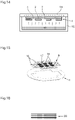
- the wafer 8 is preferably supported horizontally by a support plate 11 as illustrated in figures 12 and 13 , which can be handled manually or by a robot.
- This support plate 11 is in a material compatible with the oxidation treatment, for example quartz, silicon or silicon carbide.
- spacers 12 which support the wafer 8 in zones which do not contain components (in particular between the components).
- Plate 8 is prevented from moving horizontally by retaining elements 13 cooperating with the periphery of plate 8.
- Spacers 12 and retaining elements 13 are generally cylindrical in shape.
- the support plate 11 are integral with the support plate 11, for example fixed to the support plate 11 by bayonet type connections. They are made, for example, of quartz or of silicon carbide, and may be of the same material or of different materials. In a preferred embodiment, the support plate 11 is made of silicon and the spacers and retaining elements 12, 13 are made of quartz. Such a support plate 11 with its spacers 12 and retaining elements 13 can also be used during the step of figure 11 when this consists of a CVD or PVD deposit operation.
- the wafer 8 is placed on the support plate 11 in an upturned position with respect to the oxidation treatment of the figure 7 .
- the wafer 8 is placed on the support plate 11 in an upturned position with respect to the oxidation treatment of the figure 9 .
- the step of releasing the wafer 8 from the substrate 1 can be implemented by eliminating all of the lower layer of silicon 3 and all of the intermediate layer of silicon oxide 4 by chemical etching or plasma etching. It is also possible to remove the lower layer of silicon 3 and the intermediate layer of silicon oxide 4 only on the back of the components or groups of components, the wafer 8 then keeping part of these layers 3, 4. However, these operations are long and costly.
- the wafer 8 is preferably formed by a part of the upper layer of silicon 2 and its release from the substrate 1 is implemented in the manner explained below and illustrated in figures 14 and 15 .
- the etched substrate 1 is fixed as shown in figure 5 against a heating element 14 in a closed chamber 15 ( figure 14 ), the upper layer of silicon 2 being oriented downwards, the lower layer of silicon 3, therefore oriented upwards, being against the heating element 14.
- the method of fixing the substrate 1 against the heating element 14 can be electrostatic (by application of an electric field) or mechanical.
- a hydrofluoric acid (HF) solution is added to chamber 15, out of contact with substrate 1.
- the hydrofluoric acid vapors which then saturate the interior of chamber 15 etch the intermediate layer of silicon oxide 4, without attacking the silicon.
- the heating element 14, regulated in temperature prevents the condensation of the water produced by the reaction between the hydrofluoric acid and the silicon oxide, condensation which would cause sticking between the part to be released and the rest of the substrate 1.
- the part to be released namely the wafer 8 is defined beforehand by a groove made during the etching of the upper layer of silicon 2 and which forms the perimeter of the wafer 8.
- openings 16 for example in the form of hatching as depicted in figure 15 , are engraved in the wafer 8 around a central zone 17 comprising the components. These openings 16 allow the passage of hydrofluoric acid vapor.
- the figure 15 shows an example of plate 8 having a shape consisting of rectangular or square parts. Other shapes can of course be envisaged, for example the circular shape. To the figure 15 one can see the horological components 18 carried by the wafer 8, here made up of hairsprings. These timepiece components have been represented in reduced numbers compared to their real number, in order to facilitate reading of the drawing.
- the horological components manufactured by the process according to the invention can have very precise dimensions and good surface conditions which will improve the operating precision and the efficiency of the mechanisms which will use them.
- the watch components would then have a composite structure comprising one or more intermediate layers of silicon oxide.
- the photosensitive lacquer mask 5 which is used to structure the upper layer of silicon 2 ( figure 3 ) could be replaced by a silicon oxide mask. It would also be possible to combine a mask of photosensitive lacquer and a mask of silicon oxide to produce, by etching in the upper layer of silicon or in a group of upper layers, multilevel timepiece components.
- the substrate could be etched from its two faces.
- the layer or layers of silicon oxides used to stop the etching could be reinforced by one or layers of the parylene type.
- the present invention does not exclude either the use of one or more metal layers to stop the etching.
Landscapes
- Chemical & Material Sciences (AREA)
- Engineering & Computer Science (AREA)
- Metallurgy (AREA)
- Physics & Mathematics (AREA)
- General Physics & Mathematics (AREA)
- Organic Chemistry (AREA)
- Materials Engineering (AREA)
- Manufacturing & Machinery (AREA)
- Chemical Kinetics & Catalysis (AREA)
- Mechanical Engineering (AREA)
- Crystallography & Structural Chemistry (AREA)
- Inorganic Chemistry (AREA)
- General Chemical & Material Sciences (AREA)
- Thermal Sciences (AREA)
- Micromachines (AREA)
- Crystals, And After-Treatments Of Crystals (AREA)
- Weting (AREA)
Description
La présente invention porte sur un procédé de fabrication de composants horlogers, tels que des spiraux, des ancres, des roues, des aiguilles, des bascules, des leviers, des ressorts ou des balanciers, en silicium.The present invention relates to a process for manufacturing watch components, such as hairsprings, levers, wheels, hands, levers, levers, springs or balances, in silicon.
Des procédés de fabrication de composants horlogers en silicium ont été décrits notamment dans les documents
La présente invention vise à proposer un procédé permettant de fabriquer des composants horlogers en silicium de grande qualité.The present invention aims to provide a method for manufacturing high quality silicon watch components.
A cette fin il est prévu un procédé selon la revendication 1 ou la revendication 2 et les revendications qui en dépendent.To this end there is provided a method according to claim 1 or
D'autres caractéristiques et avantages de la présente invention apparaîtront à la lecture de la description détaillée suivante faite en référence aux dessins annexés dans lesquels :
- les
figures 1 à 11 montrent schématiquement des étapes successives d'un procédé selon un mode de réalisation particulier de l'invention ; - les
figures 12 et 13 sont respectivement une vue en perspective et une vue de profil d'un organe de support utilisé dans le procédé selon le mode de réalisation particulier de l'invention pour supporter une plaquette de silicium pendant un traitement d'oxydation thermique de cette dernière ; - les
figures 14 et 15 montrent schématiquement une étape du procédé selon le mode de réalisation particulier de l'invention, dans laquelle une plaquette de silicium gravée est libérée d'un substrat composite ; - la
figure 16 montre un substrat composite à partir duquel peut être mis en œuvre un procédé selon un autre mode de réalisation de l'invention.
- them
figures 1 to 11 schematically show successive steps of a method according to a particular embodiment of the invention; - them
figures 12 and 13 are respectively a perspective view and a side view of a support member used in the method according to the particular embodiment of the invention to support a silicon wafer during a thermal oxidation treatment of the latter; - them
figures 14 and 15 schematically show a step of the method according to the particular embodiment of the invention, in which an etched silicon wafer is released from a composite substrate; - the
figure 16 shows a composite substrate from which a method according to another embodiment of the invention can be implemented.
Un procédé de fabrication de composants horlogers en silicium, notamment pour montres-bracelets, comprend selon un mode de réalisation particulier de l'invention les étapes successives illustrées aux
A une première étape (
A une deuxième étape (
A une étape suivante (
Le masque de laque photosensible 5 est ensuite éliminé par gravure chimique ou gravure plasma (
A une étape suivante (
Puis la plaquette 8 est placée dans un four d'oxydation pour être soumise à un traitement thermique, typiquement entre 600°C et 1300°C, oxydant toute la surface extérieure des composants horlogers (
A ce stade du procédé, on peut mesurer des caractéristiques physiques des composants horlogers ou de certains d'entre eux, notamment leurs dimensions. Grâce à l'étape précédente d'oxydation - désoxydation, ces caractéristiques physiques sont bien définies et leur mesure peut donc être précise, n'étant pas perturbée par les défauts de surface. Dans le cas de spiraux, on peut déterminer leur raideur. Pour un spiral donné, la raideur peut être déterminée en couplant le spiral, alors qu'il est encore attaché à la plaquette 8 ou détaché de la plaquette 8, à un balancier d'inertie prédéterminée, en mesurant la fréquence de l'ensemble balancier-spiral et en déduisant de cette mesure, par calcul, la raideur du spiral. On peut plus particulièrement mettre en oeuvre le procédé décrit dans la demande de
A encore une autre étape du procédé (
A une étape finale, les composants horlogers sont détachés de la structure de base de la plaquette 8.In a final step, the watch components are detached from the basic structure of the
Durant les étapes d'oxydation (
De préférence, durant le traitement d'oxydation de la
L'étape de libération de la plaquette 8 du substrat 1 (
On fixe le substrat 1 gravé tel que montré à la
La partie à libérer, à savoir la plaquette 8, est définie préalablement par une saignée réalisée lors de la gravure de la couche supérieure de silicium 2 et qui forme le pourtour de la plaquette 8. Pendant cette même gravure de la couche supérieure de silicium 2, des ouvertures 16, par exemple en forme de hachures comme représenté à la
La
Les composants horlogers fabriqués par le procédé selon l'invention peuvent avoir des dimensions très précises et de bons états de surface qui amélioreront la précision de fonctionnement et le rendement des mécanismes qui les utiliseront.The horological components manufactured by the process according to the invention can have very precise dimensions and good surface conditions which will improve the operating precision and the efficiency of the mechanisms which will use them.
Des modifications du procédé selon l'invention tel que décrit ci-dessus sont bien entendu possibles.Modifications of the process according to the invention as described above are of course possible.
Par exemple, bien que les deux étapes d'oxydation - désoxydation (
On pourrait aussi partir d'un substrat double ou triple SOI, voire plus, c'est-à-dire d'un substrat comprenant plus de deux couches de silicium séparées par des couches intermédiaires d'oxyde de silicium, comme le substrat 20 montré à la
Le masque de laque photosensible 5 qui sert à structurer la couche supérieure de silicium 2 (
Dans d'autres variantes, on pourrait graver le substrat depuis ses deux faces.In other variants, the substrate could be etched from its two faces.
La ou les couches d'oxydes de silicium servant à arrêter la gravure pourraient être renforcées par une ou des couches de type parylène.The layer or layers of silicon oxides used to stop the etching could be reinforced by one or layers of the parylene type.
Enfin, la présente invention n'exclut pas non plus l'utilisation d'une ou plusieurs couches métalliques pour arrêter la gravure.Finally, the present invention does not exclude either the use of one or more metal layers to stop the etching.
Claims (17)
- A method of manufacturing timepiece components comprising the following steps:a) providing a substrate (1) comprising a first silicon layer (2), a second silicon layer (3) and, in between, an intermediate silicon oxide layer (4),b) etching the first silicon layer (2) to form therein the timepiece components,c) releasing from the substrate (1) a wafer (8) formed by at least all or part of the etched, first silicon layer (2) and comprising the timepiece components,d) thermally oxidizing and then deoxidizing the timepiece components,e) forming by thermal oxidation or deposition a silicon oxide layer (10) on the timepiece components, andf) detaching the timepiece components from the wafer (8).
- A method of manufacturing timepiece components comprising the following steps :a) providing a substrate (20) comprising silicon layers interleaved with silicon oxide layers,b) etching a group of layers of the substrate to form therein the timepiece components,c) releasing from the substrate a wafer formed by at least all or part of the group of layers and comprising the timepiece components,d) thermally oxidizing and then deoxidizing the timepiece components,e) forming by thermal oxidation or deposition a silicon oxide layer on the timepiece components, andf) detaching the timepiece components from the wafer.
- A method according to claim 1 or 2, wherein the etching in step b) comprises a deep reactive ion etching.
- A method according to any of claims 1 to 3, comprising between steps d) and e) an additional step consisting of thermally oxidizing and then deoxidizing the timepiece components.
- A method according to claim 4, wherein step d) serves to improve the surface finish of the timepiece components and said additional step serves to adjust the stiffness of hairsprings constituting the timepiece components.
- A method according to claim 4 or 5, wherein during the thermal oxidation operation of said additional step the wafer (8) is in an inverted position with respect to the thermal oxidation operation of step d).
- A method according to any of claims 4 to 6, wherein during step e) the wafer (8) is in an inverted position with respect to the thermal oxidation operation of said additional step.
- A method according to any of claims 1 to 7, wherein during the thermal oxidation operation(s) the wafer (8) is supported by a support member (11, 12, 13) comprising a support plate (11) and spacers (12) and retaining elements (13) carried by the support plate (11), the spacers (12) maintaining a gap between the wafer (8) and the support plate (11), the retaining elements (13) preventing the wafer (8) from moving horizontally.
- A method according to claim 8, wherein the spacers (12) support the wafer (8) in areas of the wafer (8) not comprising any timepiece component.
- A method according to claim 8 or 9, wherein the support plate (11) is made of silicon, quartz or silicon carbide.
- A method according to any of claims 8 to 10, wherein the spacers (12) and the retaining elements (13) are made of quartz or silicon carbide.
- A method according to any of claims 8 to 11, wherein the spacers (12) and the retaining elements (13) are fixed to the support plate (11) by bayonet-type connections.
- A method according to any of claims 1 and 3 to 12, wherein step c) comprises an operation of vapor-phase etching the intermediate silicon oxide layer (4).
- A method according to any of claims 1 and 3 to 13, wherein the wafer (8) released in step c) is formed by a part of the etched, first silicon layer (2).
- A method according to any of claims 1 and 3 to 14, wherein in step b) a groove is etched in the first silicon layer (2) in order to define the peripheral edge of the wafer (8) to be released in step c).
- A method according to any of claims 1 and 3 to 15, wherein in step b) openings (16) are etched in the first silicon layer (2) around a central area (17) where the timepiece components (18) are etched, these openings (16) allowing the passage of an etching agent for etching the intermediate silicon oxide layer (4) during step c).
- A method according to any of claims 1 to 16, wherein the timepiece components comprise at least one of the following types of components: hairsprings (18), anchors, wheels, hands, rockers, levers, springs, balances, or parts of such components.
Priority Applications (2)
| Application Number | Priority Date | Filing Date | Title |
|---|---|---|---|
| EP24216887.0A EP4492160A2 (en) | 2018-03-20 | 2019-03-19 | Support member for the thermal treatment of a wafer |
| EP21182494.1A EP3907567B1 (en) | 2018-03-20 | 2019-03-19 | Support member for thermal treatment of a plate |
Applications Claiming Priority (2)
| Application Number | Priority Date | Filing Date | Title |
|---|---|---|---|
| EP18162729.0A EP3543795A1 (en) | 2018-03-20 | 2018-03-20 | Method for manufacturing silicon clock components |
| PCT/IB2019/052198 WO2019180596A1 (en) | 2018-03-20 | 2019-03-19 | Method for producing silicon watchmaking components |
Related Child Applications (3)
| Application Number | Title | Priority Date | Filing Date |
|---|---|---|---|
| EP21182494.1A Division EP3907567B1 (en) | 2018-03-20 | 2019-03-19 | Support member for thermal treatment of a plate |
| EP21182494.1A Division-Into EP3907567B1 (en) | 2018-03-20 | 2019-03-19 | Support member for thermal treatment of a plate |
| EP24216887.0A Division EP4492160A2 (en) | 2018-03-20 | 2019-03-19 | Support member for the thermal treatment of a wafer |
Publications (2)
| Publication Number | Publication Date |
|---|---|
| EP3769162A1 EP3769162A1 (en) | 2021-01-27 |
| EP3769162B1 true EP3769162B1 (en) | 2022-08-10 |
Family
ID=61691846
Family Applications (4)
| Application Number | Title | Priority Date | Filing Date |
|---|---|---|---|
| EP18162729.0A Withdrawn EP3543795A1 (en) | 2018-03-20 | 2018-03-20 | Method for manufacturing silicon clock components |
| EP21182494.1A Active EP3907567B1 (en) | 2018-03-20 | 2019-03-19 | Support member for thermal treatment of a plate |
| EP19717200.0A Active EP3769162B1 (en) | 2018-03-20 | 2019-03-19 | Method for manufacturing silicon clock components |
| EP24216887.0A Pending EP4492160A2 (en) | 2018-03-20 | 2019-03-19 | Support member for the thermal treatment of a wafer |
Family Applications Before (2)
| Application Number | Title | Priority Date | Filing Date |
|---|---|---|---|
| EP18162729.0A Withdrawn EP3543795A1 (en) | 2018-03-20 | 2018-03-20 | Method for manufacturing silicon clock components |
| EP21182494.1A Active EP3907567B1 (en) | 2018-03-20 | 2019-03-19 | Support member for thermal treatment of a plate |
Family Applications After (1)
| Application Number | Title | Priority Date | Filing Date |
|---|---|---|---|
| EP24216887.0A Pending EP4492160A2 (en) | 2018-03-20 | 2019-03-19 | Support member for the thermal treatment of a wafer |
Country Status (5)
| Country | Link |
|---|---|
| US (2) | US11880165B2 (en) |
| EP (4) | EP3543795A1 (en) |
| JP (2) | JP2021518548A (en) |
| CN (2) | CN111868637B (en) |
| WO (1) | WO2019180596A1 (en) |
Families Citing this family (11)
| Publication number | Priority date | Publication date | Assignee | Title |
|---|---|---|---|---|
| EP3543796A1 (en) * | 2018-03-21 | 2019-09-25 | Nivarox-FAR S.A. | Method for manufacturing a silicon hairspring |
| EP3839642A1 (en) | 2019-12-20 | 2021-06-23 | Patek Philippe SA Genève | Method for manufacturing timepiece springs and etching mask for such a method |
| EP3865954A1 (en) * | 2020-02-12 | 2021-08-18 | Nivarox-FAR S.A. | Method for manufacturing a device with flexible single-piece silicon sheets, for timepieces |
| EP3882714A1 (en) * | 2020-03-19 | 2021-09-22 | Patek Philippe SA Genève | Method for manufacturing a silicon clock component |
| EP3882710A1 (en) * | 2020-03-19 | 2021-09-22 | Patek Philippe SA Genève | Method for manufacturing a silicon-based clock component |
| EP3907565A1 (en) | 2020-05-07 | 2021-11-10 | Patek Philippe SA Genève | Method for manufacturing a silicon timepiece component |
| NL2028796B1 (en) | 2021-07-20 | 2023-01-23 | Flexous Mech Ip B V | Method of manufacturing a plurality of mechanical resonators in a manufacturing wafer |
| EP4212965A1 (en) | 2022-01-14 | 2023-07-19 | Richemont International S.A. | Method for limiting the deformation of a silicon timepiece |
| CH719414A2 (en) | 2022-02-11 | 2023-08-31 | Sigatec Sa | Process for manufacturing a silicon part. |
| EP4312084A1 (en) | 2022-07-26 | 2024-01-31 | Nivarox-FAR S.A. | Method for manufacturing a silicon hairspring |
| CH720935A1 (en) | 2023-07-11 | 2025-01-15 | Richemont Int Sa | Manufacturing process of silicon watch components on an SOI wafer |
Citations (20)
| Publication number | Priority date | Publication date | Assignee | Title |
|---|---|---|---|---|
| US4400861A (en) | 1981-11-27 | 1983-08-30 | Oyo Instruments, Inc. | Fabrication of seismic springs from sheets |
| EP0732635A1 (en) | 1995-03-17 | 1996-09-18 | C.S.E.M. Centre Suisse D'electronique Et De Microtechnique Sa | Micromechanical element and process for its manufacture |
| US6192603B1 (en) | 1998-08-26 | 2001-02-27 | Sony Corporation | Vacuum processing apparatus and magnetic seal rotary bearing unit |
| EP1422436A1 (en) | 2002-11-25 | 2004-05-26 | CSEM Centre Suisse d'Electronique et de Microtechnique SA | Spiral watch spring and its method of production |
| SG112005A1 (en) | 2003-12-29 | 2005-06-29 | Sony Corp | A surface treatment for use in the fabrication of mems devices |
| WO2007000271A1 (en) | 2005-06-28 | 2007-01-04 | Eta Sa Manufacture Horlogere Suisse | Reinforced micromechanical part |
| US20070026614A1 (en) | 2005-07-27 | 2007-02-01 | The Regents Of The University Of California | CMOS-compatible high-performance microscanners, including structures, high-yield simplified fabrication methods and applications |
| WO2009068091A1 (en) | 2007-11-28 | 2009-06-04 | Manufacture Et Fabrique De Montres Et Chronomètres Ulysse Nardin Le Locle S.A. | Mechanical oscillator having an optimized thermoelastic coefficient |
| WO2010057777A1 (en) | 2008-11-21 | 2010-05-27 | Nivarox-Far S.A. | Method for making a micromechanical part |
| CH703051A2 (en) | 2010-04-21 | 2011-10-31 | Team Smartfish Gmbh | Coil spring for a movement and method of manufacture. |
| JP2014168819A (en) | 2013-03-01 | 2014-09-18 | Nippon Telegr & Teleph Corp <Ntt> | Production method of micromechanical structure |
| EP2799939A1 (en) | 2013-04-30 | 2014-11-05 | Universo S.A. | Support for the treatment of micromechanical parts |
| WO2015113973A1 (en) | 2014-01-29 | 2015-08-06 | Cartier Création Studio Sa | Thermally compensated hairspring made from ceramic comprising silicon in the composition of same and method for adjusting same |
| JP2015179067A (en) | 2014-02-26 | 2015-10-08 | シチズンホールディングス株式会社 | Manufacturing method of balance spring |
| EP2937311A1 (en) | 2014-04-25 | 2015-10-28 | Rolex Sa | Method for manufacturing a reinforced timepiece component, corresponding timepiece component and timepiece |
| WO2016128694A1 (en) | 2015-02-13 | 2016-08-18 | Tronic's Microsystems | Mechanical oscillator and associated production method |
| JP2016161394A (en) | 2015-03-02 | 2016-09-05 | シチズンホールディングス株式会社 | Timepiece component |
| JP2016173356A (en) | 2015-03-16 | 2016-09-29 | シチズンホールディングス株式会社 | Manufacturing method of silicon machine component |
| US20170115063A1 (en) | 2015-10-26 | 2017-04-27 | Sunedison Semiconductor Limited (Uen201334164H) | Semiconductor wafer support ring for heat treatment |
| EP3181938A1 (en) | 2015-12-18 | 2017-06-21 | CSEM Centre Suisse d'Electronique et de Microtechnique SA - Recherche et Développement | Method for manufacturing a hairspring with a predetermined stiffness by removing material |
Family Cites Families (21)
| Publication number | Priority date | Publication date | Assignee | Title |
|---|---|---|---|---|
| US6706202B1 (en) * | 2000-09-28 | 2004-03-16 | Xerox Corporation | Method for shaped optical MEMS components with stressed thin films |
| JP2002341054A (en) * | 2001-05-11 | 2002-11-27 | Seiko Instruments Inc | Hair spring, its structural body, and speed governing mechanism and timepiece using it |
| TWI258208B (en) * | 2004-01-14 | 2006-07-11 | Mosel Vitelic Inc | Loading device for wafer and the supporting structure thereof |
| US8614110B1 (en) * | 2006-07-25 | 2013-12-24 | The United States Of America As Represented By The Secretary Of The Navy | Method for fabricating a dual-crystalline silicon suspension system using pre-fabricated cavities |
| CH714952B1 (en) * | 2007-05-08 | 2019-10-31 | Patek Philippe Sa Geneve | Watchmaking component, its method of manufacture and application of this method. |
| US8030133B2 (en) * | 2008-03-28 | 2011-10-04 | Icemos Technology Ltd. | Method of fabricating a bonded wafer substrate for use in MEMS structures |
| CH701499B1 (en) | 2009-07-23 | 2016-09-15 | Montres Breguet Sa | A method of manufacturing a micromechanical part reinforced silicon. |
| EP2423764B1 (en) | 2010-08-31 | 2013-03-27 | Rolex S.A. | Device for measuring the torque of a hairspring |
| EP2472340B1 (en) | 2011-01-03 | 2021-03-03 | Patek Philippe SA Genève | Timepiece component and method for manufacturing same |
| CN103930837B (en) * | 2011-09-29 | 2017-05-03 | 劳力士有限公司 | Integral assembly of a hairspring and a collet |
| US9034754B2 (en) * | 2012-05-25 | 2015-05-19 | LuxVue Technology Corporation | Method of forming a micro device transfer head with silicon electrode |
| CH707797A1 (en) * | 2013-03-28 | 2014-09-30 | Silicior Sa | A method of manufacturing a micro-mechanical part substantially flat, and micro-mechanical part comprising at least a portion formed of silicon oxide. |
| EP2799940B1 (en) * | 2013-04-30 | 2019-07-17 | The Swatch Group Management Services AG | Packaging for hands of watches |
| EP3069377A4 (en) * | 2013-11-13 | 2017-05-31 | Michigan Technological University | Silicon nanowire-based sensor arrays |
| JP2015179013A (en) | 2014-03-19 | 2015-10-08 | シチズンホールディングス株式会社 | Manufacturing method of balance spring |
| JP2016133495A (en) | 2015-01-22 | 2016-07-25 | シチズンホールディングス株式会社 | Method of manufacturing timepiece component and timepiece component |
| JP6554328B2 (en) | 2015-05-29 | 2019-07-31 | 株式会社Screenホールディングス | Heat treatment equipment |
| EP3109199B1 (en) * | 2015-06-25 | 2022-05-11 | Nivarox-FAR S.A. | Silicon-based part with at least one chamfer and method for manufacturing same |
| EP3109200B1 (en) * | 2015-06-25 | 2023-06-28 | Nivarox-FAR S.A. | Micromechanical part with reduced contact surface and method for manufacturing same |
| EP3088969B1 (en) * | 2016-03-17 | 2018-12-26 | Sigatec SA | Thermocompensated hairspring and method of production thereof |
| TWI796444B (en) | 2018-03-20 | 2023-03-21 | 瑞士商百達翡麗日內瓦股份有限公司 | Method for manufacturing timepiece thermocompensated hairsprings of precise stiffness |
-
2018
- 2018-03-20 EP EP18162729.0A patent/EP3543795A1/en not_active Withdrawn
-
2019
- 2019-03-19 WO PCT/IB2019/052198 patent/WO2019180596A1/en unknown
- 2019-03-19 US US16/980,126 patent/US11880165B2/en active Active
- 2019-03-19 JP JP2020550771A patent/JP2021518548A/en active Pending
- 2019-03-19 CN CN201980020156.7A patent/CN111868637B/en active Active
- 2019-03-19 EP EP21182494.1A patent/EP3907567B1/en active Active
- 2019-03-19 EP EP19717200.0A patent/EP3769162B1/en active Active
- 2019-03-19 EP EP24216887.0A patent/EP4492160A2/en active Pending
- 2019-03-19 CN CN202210052591.1A patent/CN114460826B/en active Active
-
2023
- 2023-09-11 JP JP2023146855A patent/JP2023164549A/en active Pending
- 2023-12-08 US US18/533,303 patent/US20240103442A1/en active Pending
Patent Citations (21)
| Publication number | Priority date | Publication date | Assignee | Title |
|---|---|---|---|---|
| US4400861A (en) | 1981-11-27 | 1983-08-30 | Oyo Instruments, Inc. | Fabrication of seismic springs from sheets |
| EP0732635A1 (en) | 1995-03-17 | 1996-09-18 | C.S.E.M. Centre Suisse D'electronique Et De Microtechnique Sa | Micromechanical element and process for its manufacture |
| US6192603B1 (en) | 1998-08-26 | 2001-02-27 | Sony Corporation | Vacuum processing apparatus and magnetic seal rotary bearing unit |
| EP1422436A1 (en) | 2002-11-25 | 2004-05-26 | CSEM Centre Suisse d'Electronique et de Microtechnique SA | Spiral watch spring and its method of production |
| SG112005A1 (en) | 2003-12-29 | 2005-06-29 | Sony Corp | A surface treatment for use in the fabrication of mems devices |
| WO2007000271A1 (en) | 2005-06-28 | 2007-01-04 | Eta Sa Manufacture Horlogere Suisse | Reinforced micromechanical part |
| US20070026614A1 (en) | 2005-07-27 | 2007-02-01 | The Regents Of The University Of California | CMOS-compatible high-performance microscanners, including structures, high-yield simplified fabrication methods and applications |
| WO2009068091A1 (en) | 2007-11-28 | 2009-06-04 | Manufacture Et Fabrique De Montres Et Chronomètres Ulysse Nardin Le Locle S.A. | Mechanical oscillator having an optimized thermoelastic coefficient |
| WO2010057777A1 (en) | 2008-11-21 | 2010-05-27 | Nivarox-Far S.A. | Method for making a micromechanical part |
| CH703051A2 (en) | 2010-04-21 | 2011-10-31 | Team Smartfish Gmbh | Coil spring for a movement and method of manufacture. |
| JP2014168819A (en) | 2013-03-01 | 2014-09-18 | Nippon Telegr & Teleph Corp <Ntt> | Production method of micromechanical structure |
| EP2799939A1 (en) | 2013-04-30 | 2014-11-05 | Universo S.A. | Support for the treatment of micromechanical parts |
| WO2015113973A1 (en) | 2014-01-29 | 2015-08-06 | Cartier Création Studio Sa | Thermally compensated hairspring made from ceramic comprising silicon in the composition of same and method for adjusting same |
| JP2015179067A (en) | 2014-02-26 | 2015-10-08 | シチズンホールディングス株式会社 | Manufacturing method of balance spring |
| EP2937311A1 (en) | 2014-04-25 | 2015-10-28 | Rolex Sa | Method for manufacturing a reinforced timepiece component, corresponding timepiece component and timepiece |
| WO2016128694A1 (en) | 2015-02-13 | 2016-08-18 | Tronic's Microsystems | Mechanical oscillator and associated production method |
| JP2016161394A (en) | 2015-03-02 | 2016-09-05 | シチズンホールディングス株式会社 | Timepiece component |
| JP2016173356A (en) | 2015-03-16 | 2016-09-29 | シチズンホールディングス株式会社 | Manufacturing method of silicon machine component |
| JP2016173355A (en) | 2015-03-16 | 2016-09-29 | シチズンホールディングス株式会社 | Manufacturing method of machine component |
| US20170115063A1 (en) | 2015-10-26 | 2017-04-27 | Sunedison Semiconductor Limited (Uen201334164H) | Semiconductor wafer support ring for heat treatment |
| EP3181938A1 (en) | 2015-12-18 | 2017-06-21 | CSEM Centre Suisse d'Electronique et de Microtechnique SA - Recherche et Développement | Method for manufacturing a hairspring with a predetermined stiffness by removing material |
Non-Patent Citations (17)
| Title |
|---|
| "Académie francaises", 31 December 2022, ACADÉMIE FRANCAISES, article ANONYMOUS: "Horloger, Horlogère", XP093108244 |
| "ACADÉMIE FRANCAISES:", 31 December 2022, ACADÉMIE FRANCAISES, article ANONYMOUS: "Horlogerie", XP093108240 |
| ANONYMOUS: " HF VAPOR ETCHER - HFVE STANDARD", A.M.M.T., 12 February 2016 (2016-02-12), XP093157640, Retrieved from the Internet <URL:https://www.ammt.com/support/files/AMMT_PI_HFVEStandard.pdf> |
| ANONYMOUS: "Microsystème électromécanique", WIKIPÉDIA, L'ENCYCLOPÉDIE LIBRE, 27 April 2023 (2023-04-27), XP093108246, Retrieved from the Internet <URL:https://fr.wikipedia.org/wiki/Microsyst%C3%A8me_%C3%A9lectrom%C3%A9canique> [retrieved on 20231204] |
| ANONYMOUS: "Qualcomm Toq smart watch to go for sale on Dec.2, but with an entry price of US$349.99, is still expensive luxury", 19 November 2013 (2013-11-19), XP093157650, Retrieved from the Internet <URL:https://english.etnews.com/20131119200007> |
| ANONYMOUS: "Silicon on insulator", WIKIPEDIA, 16 November 2018 (2018-11-16), pages 1 - 6, XP093217528, Retrieved from the Internet <URL:https://en.wikipedia.org/w/index.php?title=Silicon_on_insulator&oldid=869160080> |
| G.V. HERRERA ; T. BAUER ; M.G. BLAIN ; P.E. DODD ; R. DONDERO ; E.J. GARCIA ; P.C. GALAMBOS ; D.L. HETHERINGTON ; J.J. HUDGENS ; F: "SOI-enabled MEMS processes lead to novel mechanical, optical, and atomic physics devices", 2008 IEEE INTERNATIONAL SOI CONFERENCE PROCEEDINGS, 6 October 2008 (2008-10-06), Piscataway, NJ, USA , pages 5 - 8, XP031351829, ISBN: 978-1-4244-1954-8 |
| HERRERA, G.V. ET AL.: "SOI-Enabled MEMS Processes Lead to Novel Mechanical, Optical and Atomic Physics Devices", 2008 IEEE INTERNATIONAL SOI CONFÉRENCE PROCEEDINGS, 2008, pages 5 - 8, XP031351829 |
| LAURA MCCREDDIE-DOAK: "This is where Patek Philippe develops the watches of the future | WIRED UK", 31 December 2017 (2017-12-31), XP055699852, Retrieved from the Internet <URL:https://www.wired.co.uk/article/patek-philippes-aquanaut-travel-time-is-packed-with-innovation> [retrieved on 20200529] |
| NOELL W., CLERC P.-A., JEANNERET S., HOOGERWERF A., NIEDERMANN P., PERRET A., DE ROOIJ N.F.: "MEMS for a watches", MICRO ELECTRO MECHANICAL SYSTEMS, 2004. 17TH IEEE INTERNATIONAL CONFER ENCE ON. (MEMS) MAASTRICHT, NETHERLANDS 25-29 JAN. 2004, PISCATAWAY, NJ, USA,IEEE, US, 25 January 2004 (2004-01-25) - 29 January 2004 (2004-01-29), US , pages 1 - 4, XP010767811, ISBN: 978-0-7803-8265-7, DOI: 10.1109/MEMS.2004.1290507 |
| P. CLARKE: "MEMS scanner projects Bosch Sensortec into displays, user interfaces", EENEWS ANALOG, 27 February 2017 (2017-02-27), XP093157648 |
| SARI, I. ET AL.: "A Full Wafer Dicing Free Dry Release Process For MEMS Devices", PROC. EUROSENSORS XXIV, PROCEDIA ENGINEERING, vol. 5, 2010, pages 850 - 853, XP027483798, DOI: 10.1016/j.proeng.2010.09.242 |
| SIDEWALL SMOOTHING OF BOSCH SCALLOPS VIA THERMAL OXIDATION, 7 June 2012 (2012-06-07), XP055699858, Retrieved from the Internet <URL:https://www.nanofab.ualberta.ca/wp- content/uploads/downloads/2012/06/Sidewall-smoothing-using- thermal-oxidation-steps 2.pd> |
| SYLVAIN AUBRY: "Théorie des échappements", July 2016, FEDERATION DES ECOLES TECHNIQUES, article AUBRY, S.: "5.2 Gravure profonde du silicium (DRIE)", pages: 287-292, 368 |
| T M FAHIM AMIN: "Design and Fabrication of Micro-electro-mechanical Systems Actuators for Application in External Cavity Tunable Lasers", DOCTORAL THESIS, UNIVERSITY OF ALBERTA, 1 January 2014 (2014-01-01), XP093157631 |
| ZISHAN ALI SYED MOHAMMED, M.A.S. OLIMPOA , D.P. POENARA , S. ADITYA: "Smoothening of scalloped DRIE trench walls", MATERIALS SCIENCE IN SEMICONDUCTOR PROCESSING., ELSEVIER SCIENCE PUBLISHERS B.V., BARKING., UK, vol. 63, 1 June 2017 (2017-06-01), UK , pages 83 - 89, XP093157619, ISSN: 1369-8001, DOI: 10.1016/j.mssp.2017.02.006 |
| ZUJUN SHI, SHIQIAN SHAO, YI WANG: "Improved the Surface Roughness of Silicon Nanophotonic Devices by Thermal Oxidation Method", JOURNAL OF PHYSICS: CONFERENCE SERIES, INSTITUTE OF PHYSICS PUBLISHING, BRISTOL, GB, vol. 276, 1 February 2011 (2011-02-01), GB , pages 012087, XP093157636, ISSN: 1742-6596, DOI: 10.1088/1742-6596/276/1/012087 |
Also Published As
| Publication number | Publication date |
|---|---|
| WO2019180596A1 (en) | 2019-09-26 |
| EP3543795A1 (en) | 2019-09-25 |
| CN114460826A (en) | 2022-05-10 |
| US11880165B2 (en) | 2024-01-23 |
| CN111868637B (en) | 2022-04-12 |
| EP4492160A2 (en) | 2025-01-15 |
| EP3907567A1 (en) | 2021-11-10 |
| EP3907567B1 (en) | 2025-01-08 |
| US20210026299A1 (en) | 2021-01-28 |
| CN114460826B (en) | 2024-07-09 |
| EP3769162A1 (en) | 2021-01-27 |
| CN111868637A (en) | 2020-10-30 |
| JP2023164549A (en) | 2023-11-10 |
| US20240103442A1 (en) | 2024-03-28 |
| JP2021518548A (en) | 2021-08-02 |
Similar Documents
| Publication | Publication Date | Title |
|---|---|---|
| EP3769162B1 (en) | Method for manufacturing silicon clock components | |
| EP3181938B1 (en) | Method for manufacturing a hairspring with a predetermined stiffness by removing material | |
| EP3181939B1 (en) | Method for manufacturing a hairspring with predetermined stiffness by adding material | |
| EP3769160A1 (en) | Method for manufacturing a silicon hairspring | |
| EP3181940B1 (en) | Method for manufacturing a hairspring with a predetermined stiffness by localised removal of material | |
| EP3769161B1 (en) | Method for manufacturing thermocompensated hairsprings with precise stiffness | |
| EP3915788B1 (en) | Method for manufacturing a batch of timepiece hairsprings | |
| EP3789825B1 (en) | Method for manufacturing a plurality of microparts | |
| EP3495894B1 (en) | Method for manufacturing a clock component | |
| CH714806B1 (en) | Process for manufacturing silicon watch components. | |
| EP3865954A1 (en) | Method for manufacturing a device with flexible single-piece silicon sheets, for timepieces | |
| EP1121622A1 (en) | Structure for reflection lithography mask and method for making same | |
| CH714815A2 (en) | Process for manufacturing a silicon spiral for watchmaking | |
| CH717124A2 (en) | A method of manufacturing a device with one-piece flexible silicon blades, in particular for watchmaking. | |
| EP3882714A1 (en) | Method for manufacturing a silicon clock component | |
| EP4111264A1 (en) | Silicon timepiece component for a timepiece | |
| CH718082A2 (en) | Method of manufacturing an elastic element for a micromechanical system. | |
| TW202035890A (en) | Process for fabricating a silicon hairspring | |
| EP3907565A1 (en) | Method for manufacturing a silicon timepiece component | |
| CH711960B1 (en) | A method of manufacturing a hairspring of predetermined stiffness with removal of material | |
| CH711961B1 (en) | A method of manufacturing a hairspring of predetermined stiffness, in particular with the addition of material. |
Legal Events
| Date | Code | Title | Description |
|---|---|---|---|
| STAA | Information on the status of an ep patent application or granted ep patent |
Free format text: STATUS: UNKNOWN |
|
| STAA | Information on the status of an ep patent application or granted ep patent |
Free format text: STATUS: THE INTERNATIONAL PUBLICATION HAS BEEN MADE |
|
| TPAC | Observations filed by third parties |
Free format text: ORIGINAL CODE: EPIDOSNTIPA |
|
| PUAI | Public reference made under article 153(3) epc to a published international application that has entered the european phase |
Free format text: ORIGINAL CODE: 0009012 |
|
| STAA | Information on the status of an ep patent application or granted ep patent |
Free format text: STATUS: REQUEST FOR EXAMINATION WAS MADE |
|
| 17P | Request for examination filed |
Effective date: 20200907 |
|
| AK | Designated contracting states |
Kind code of ref document: A1 Designated state(s): AL AT BE BG CH CY CZ DE DK EE ES FI FR GB GR HR HU IE IS IT LI LT LU LV MC MK MT NL NO PL PT RO RS SE SI SK SM TR |
|
| AX | Request for extension of the european patent |
Extension state: BA ME |
|
| DAV | Request for validation of the european patent (deleted) | ||
| DAX | Request for extension of the european patent (deleted) | ||
| TPAA | Information related to observations by third parties modified |
Free format text: ORIGINAL CODE: EPIDOSCTIPA |
|
| GRAP | Despatch of communication of intention to grant a patent |
Free format text: ORIGINAL CODE: EPIDOSNIGR1 |
|
| STAA | Information on the status of an ep patent application or granted ep patent |
Free format text: STATUS: GRANT OF PATENT IS INTENDED |
|
| INTG | Intention to grant announced |
Effective date: 20220422 |
|
| GRAS | Grant fee paid |
Free format text: ORIGINAL CODE: EPIDOSNIGR3 |
|
| GRAA | (expected) grant |
Free format text: ORIGINAL CODE: 0009210 |
|
| STAA | Information on the status of an ep patent application or granted ep patent |
Free format text: STATUS: THE PATENT HAS BEEN GRANTED |
|
| AK | Designated contracting states |
Kind code of ref document: B1 Designated state(s): AL AT BE BG CH CY CZ DE DK EE ES FI FR GB GR HR HU IE IS IT LI LT LU LV MC MK MT NL NO PL PT RO RS SE SI SK SM TR |
|
| REG | Reference to a national code |
Ref country code: AT Ref legal event code: REF Ref document number: 1511003 Country of ref document: AT Kind code of ref document: T Effective date: 20220815 Ref country code: CH Ref legal event code: EP |
|
| REG | Reference to a national code |
Ref country code: IE Ref legal event code: FG4D Free format text: LANGUAGE OF EP DOCUMENT: FRENCH |
|
| REG | Reference to a national code |
Ref country code: DE Ref legal event code: R096 Ref document number: 602019018114 Country of ref document: DE |
|
| REG | Reference to a national code |
Ref country code: NL Ref legal event code: MP Effective date: 20220810 |
|
| REG | Reference to a national code |
Ref country code: LT Ref legal event code: MG9D |
|
| PG25 | Lapsed in a contracting state [announced via postgrant information from national office to epo] |
Ref country code: SE Free format text: LAPSE BECAUSE OF FAILURE TO SUBMIT A TRANSLATION OF THE DESCRIPTION OR TO PAY THE FEE WITHIN THE PRESCRIBED TIME-LIMIT Effective date: 20220810 Ref country code: RS Free format text: LAPSE BECAUSE OF FAILURE TO SUBMIT A TRANSLATION OF THE DESCRIPTION OR TO PAY THE FEE WITHIN THE PRESCRIBED TIME-LIMIT Effective date: 20220810 Ref country code: PT Free format text: LAPSE BECAUSE OF FAILURE TO SUBMIT A TRANSLATION OF THE DESCRIPTION OR TO PAY THE FEE WITHIN THE PRESCRIBED TIME-LIMIT Effective date: 20221212 Ref country code: NO Free format text: LAPSE BECAUSE OF FAILURE TO SUBMIT A TRANSLATION OF THE DESCRIPTION OR TO PAY THE FEE WITHIN THE PRESCRIBED TIME-LIMIT Effective date: 20221110 Ref country code: NL Free format text: LAPSE BECAUSE OF FAILURE TO SUBMIT A TRANSLATION OF THE DESCRIPTION OR TO PAY THE FEE WITHIN THE PRESCRIBED TIME-LIMIT Effective date: 20220810 Ref country code: LV Free format text: LAPSE BECAUSE OF FAILURE TO SUBMIT A TRANSLATION OF THE DESCRIPTION OR TO PAY THE FEE WITHIN THE PRESCRIBED TIME-LIMIT Effective date: 20220810 Ref country code: LT Free format text: LAPSE BECAUSE OF FAILURE TO SUBMIT A TRANSLATION OF THE DESCRIPTION OR TO PAY THE FEE WITHIN THE PRESCRIBED TIME-LIMIT Effective date: 20220810 Ref country code: FI Free format text: LAPSE BECAUSE OF FAILURE TO SUBMIT A TRANSLATION OF THE DESCRIPTION OR TO PAY THE FEE WITHIN THE PRESCRIBED TIME-LIMIT Effective date: 20220810 |
|
| REG | Reference to a national code |
Ref country code: AT Ref legal event code: MK05 Ref document number: 1511003 Country of ref document: AT Kind code of ref document: T Effective date: 20220810 |
|
| PG25 | Lapsed in a contracting state [announced via postgrant information from national office to epo] |
Ref country code: PL Free format text: LAPSE BECAUSE OF FAILURE TO SUBMIT A TRANSLATION OF THE DESCRIPTION OR TO PAY THE FEE WITHIN THE PRESCRIBED TIME-LIMIT Effective date: 20220810 Ref country code: IS Free format text: LAPSE BECAUSE OF FAILURE TO SUBMIT A TRANSLATION OF THE DESCRIPTION OR TO PAY THE FEE WITHIN THE PRESCRIBED TIME-LIMIT Effective date: 20221210 Ref country code: HR Free format text: LAPSE BECAUSE OF FAILURE TO SUBMIT A TRANSLATION OF THE DESCRIPTION OR TO PAY THE FEE WITHIN THE PRESCRIBED TIME-LIMIT Effective date: 20220810 Ref country code: GR Free format text: LAPSE BECAUSE OF FAILURE TO SUBMIT A TRANSLATION OF THE DESCRIPTION OR TO PAY THE FEE WITHIN THE PRESCRIBED TIME-LIMIT Effective date: 20221111 |
|
| PG25 | Lapsed in a contracting state [announced via postgrant information from national office to epo] |
Ref country code: SM Free format text: LAPSE BECAUSE OF FAILURE TO SUBMIT A TRANSLATION OF THE DESCRIPTION OR TO PAY THE FEE WITHIN THE PRESCRIBED TIME-LIMIT Effective date: 20220810 Ref country code: RO Free format text: LAPSE BECAUSE OF FAILURE TO SUBMIT A TRANSLATION OF THE DESCRIPTION OR TO PAY THE FEE WITHIN THE PRESCRIBED TIME-LIMIT Effective date: 20220810 Ref country code: ES Free format text: LAPSE BECAUSE OF FAILURE TO SUBMIT A TRANSLATION OF THE DESCRIPTION OR TO PAY THE FEE WITHIN THE PRESCRIBED TIME-LIMIT Effective date: 20220810 Ref country code: DK Free format text: LAPSE BECAUSE OF FAILURE TO SUBMIT A TRANSLATION OF THE DESCRIPTION OR TO PAY THE FEE WITHIN THE PRESCRIBED TIME-LIMIT Effective date: 20220810 Ref country code: CZ Free format text: LAPSE BECAUSE OF FAILURE TO SUBMIT A TRANSLATION OF THE DESCRIPTION OR TO PAY THE FEE WITHIN THE PRESCRIBED TIME-LIMIT Effective date: 20220810 Ref country code: AT Free format text: LAPSE BECAUSE OF FAILURE TO SUBMIT A TRANSLATION OF THE DESCRIPTION OR TO PAY THE FEE WITHIN THE PRESCRIBED TIME-LIMIT Effective date: 20220810 |
|
| REG | Reference to a national code |
Ref country code: DE Ref legal event code: R026 Ref document number: 602019018114 Country of ref document: DE |
|
| PLBI | Opposition filed |
Free format text: ORIGINAL CODE: 0009260 |
|
| PLAB | Opposition data, opponent's data or that of the opponent's representative modified |
Free format text: ORIGINAL CODE: 0009299OPPO |
|
| PLAX | Notice of opposition and request to file observation + time limit sent |
Free format text: ORIGINAL CODE: EPIDOSNOBS2 |
|
| PG25 | Lapsed in a contracting state [announced via postgrant information from national office to epo] |
Ref country code: SK Free format text: LAPSE BECAUSE OF FAILURE TO SUBMIT A TRANSLATION OF THE DESCRIPTION OR TO PAY THE FEE WITHIN THE PRESCRIBED TIME-LIMIT Effective date: 20220810 Ref country code: EE Free format text: LAPSE BECAUSE OF FAILURE TO SUBMIT A TRANSLATION OF THE DESCRIPTION OR TO PAY THE FEE WITHIN THE PRESCRIBED TIME-LIMIT Effective date: 20220810 |
|
| PLAB | Opposition data, opponent's data or that of the opponent's representative modified |
Free format text: ORIGINAL CODE: 0009299OPPO |
|
| 26 | Opposition filed |
Opponent name: SIGATEC SA Effective date: 20230510 Opponent name: RICHEMONT INTERNATIONAL SA Effective date: 20230509 |
|
| R26 | Opposition filed (corrected) |
Opponent name: RICHEMONT INTERNATIONAL SA Effective date: 20230509 |
|
| P01 | Opt-out of the competence of the unified patent court (upc) registered |
Effective date: 20230521 |
|
| PG25 | Lapsed in a contracting state [announced via postgrant information from national office to epo] |
Ref country code: AL Free format text: LAPSE BECAUSE OF FAILURE TO SUBMIT A TRANSLATION OF THE DESCRIPTION OR TO PAY THE FEE WITHIN THE PRESCRIBED TIME-LIMIT Effective date: 20220810 |
|
| R26 | Opposition filed (corrected) |
Opponent name: SIGATEC SA Effective date: 20230510 |
|
| PG25 | Lapsed in a contracting state [announced via postgrant information from national office to epo] |
Ref country code: SI Free format text: LAPSE BECAUSE OF FAILURE TO SUBMIT A TRANSLATION OF THE DESCRIPTION OR TO PAY THE FEE WITHIN THE PRESCRIBED TIME-LIMIT Effective date: 20220810 |
|
| PLBB | Reply of patent proprietor to notice(s) of opposition received |
Free format text: ORIGINAL CODE: EPIDOSNOBS3 |
|
| PG25 | Lapsed in a contracting state [announced via postgrant information from national office to epo] |
Ref country code: MC Free format text: LAPSE BECAUSE OF FAILURE TO SUBMIT A TRANSLATION OF THE DESCRIPTION OR TO PAY THE FEE WITHIN THE PRESCRIBED TIME-LIMIT Effective date: 20220810 |
|
| REG | Reference to a national code |
Ref country code: BE Ref legal event code: MM Effective date: 20230331 |
|
| PG25 | Lapsed in a contracting state [announced via postgrant information from national office to epo] |
Ref country code: LU Free format text: LAPSE BECAUSE OF NON-PAYMENT OF DUE FEES Effective date: 20230319 |
|
| REG | Reference to a national code |
Ref country code: IE Ref legal event code: MM4A |
|
| PG25 | Lapsed in a contracting state [announced via postgrant information from national office to epo] |
Ref country code: IE Free format text: LAPSE BECAUSE OF NON-PAYMENT OF DUE FEES Effective date: 20230319 Ref country code: FR Free format text: LAPSE BECAUSE OF NON-PAYMENT OF DUE FEES Effective date: 20230331 |
|
| PG25 | Lapsed in a contracting state [announced via postgrant information from national office to epo] |
Ref country code: BE Free format text: LAPSE BECAUSE OF NON-PAYMENT OF DUE FEES Effective date: 20230331 |
|
| PGFP | Annual fee paid to national office [announced via postgrant information from national office to epo] |
Ref country code: DE Payment date: 20231229 Year of fee payment: 6 Ref country code: GB Payment date: 20240108 Year of fee payment: 6 |
|
| PG25 | Lapsed in a contracting state [announced via postgrant information from national office to epo] |
Ref country code: IT Free format text: LAPSE BECAUSE OF FAILURE TO SUBMIT A TRANSLATION OF THE DESCRIPTION OR TO PAY THE FEE WITHIN THE PRESCRIBED TIME-LIMIT Effective date: 20220810 |
|
| PGFP | Annual fee paid to national office [announced via postgrant information from national office to epo] |
Ref country code: CH Payment date: 20240401 Year of fee payment: 6 |
|
| PG25 | Lapsed in a contracting state [announced via postgrant information from national office to epo] |
Ref country code: BG Free format text: LAPSE BECAUSE OF FAILURE TO SUBMIT A TRANSLATION OF THE DESCRIPTION OR TO PAY THE FEE WITHIN THE PRESCRIBED TIME-LIMIT Effective date: 20220810 |
|
| PG25 | Lapsed in a contracting state [announced via postgrant information from national office to epo] |
Ref country code: BG Free format text: LAPSE BECAUSE OF FAILURE TO SUBMIT A TRANSLATION OF THE DESCRIPTION OR TO PAY THE FEE WITHIN THE PRESCRIBED TIME-LIMIT Effective date: 20220810 |
|
| APAH | Appeal reference modified |
Free format text: ORIGINAL CODE: EPIDOSCREFNO |
|
| APBP | Date of receipt of notice of appeal recorded |
Free format text: ORIGINAL CODE: EPIDOSNNOA2O |