EP3543795A1 - Method for manufacturing silicon clock components - Google Patents
Method for manufacturing silicon clock components Download PDFInfo
- Publication number
- EP3543795A1 EP3543795A1 EP18162729.0A EP18162729A EP3543795A1 EP 3543795 A1 EP3543795 A1 EP 3543795A1 EP 18162729 A EP18162729 A EP 18162729A EP 3543795 A1 EP3543795 A1 EP 3543795A1
- Authority
- EP
- European Patent Office
- Prior art keywords
- silicon
- wafer
- watch components
- components
- layer
- Prior art date
- Legal status (The legal status is an assumption and is not a legal conclusion. Google has not performed a legal analysis and makes no representation as to the accuracy of the status listed.)
- Withdrawn
Links
Images

Classifications
-
- G—PHYSICS
- G04—HOROLOGY
- G04B—MECHANICALLY-DRIVEN CLOCKS OR WATCHES; MECHANICAL PARTS OF CLOCKS OR WATCHES IN GENERAL; TIME PIECES USING THE POSITION OF THE SUN, MOON OR STARS
- G04B17/00—Mechanisms for stabilising frequency
- G04B17/04—Oscillators acting by spring tension
- G04B17/06—Oscillators with hairsprings, e.g. balance
- G04B17/066—Manufacture of the spiral spring
-
- C—CHEMISTRY; METALLURGY
- C01—INORGANIC CHEMISTRY
- C01B—NON-METALLIC ELEMENTS; COMPOUNDS THEREOF; METALLOIDS OR COMPOUNDS THEREOF NOT COVERED BY SUBCLASS C01C
- C01B33/00—Silicon; Compounds thereof
- C01B33/02—Silicon
-
- C—CHEMISTRY; METALLURGY
- C23—COATING METALLIC MATERIAL; COATING MATERIAL WITH METALLIC MATERIAL; CHEMICAL SURFACE TREATMENT; DIFFUSION TREATMENT OF METALLIC MATERIAL; COATING BY VACUUM EVAPORATION, BY SPUTTERING, BY ION IMPLANTATION OR BY CHEMICAL VAPOUR DEPOSITION, IN GENERAL; INHIBITING CORROSION OF METALLIC MATERIAL OR INCRUSTATION IN GENERAL
- C23C—COATING METALLIC MATERIAL; COATING MATERIAL WITH METALLIC MATERIAL; SURFACE TREATMENT OF METALLIC MATERIAL BY DIFFUSION INTO THE SURFACE, BY CHEMICAL CONVERSION OR SUBSTITUTION; COATING BY VACUUM EVAPORATION, BY SPUTTERING, BY ION IMPLANTATION OR BY CHEMICAL VAPOUR DEPOSITION, IN GENERAL
- C23C14/00—Coating by vacuum evaporation, by sputtering or by ion implantation of the coating forming material
- C23C14/06—Coating by vacuum evaporation, by sputtering or by ion implantation of the coating forming material characterised by the coating material
- C23C14/08—Oxides
-
- C—CHEMISTRY; METALLURGY
- C23—COATING METALLIC MATERIAL; COATING MATERIAL WITH METALLIC MATERIAL; CHEMICAL SURFACE TREATMENT; DIFFUSION TREATMENT OF METALLIC MATERIAL; COATING BY VACUUM EVAPORATION, BY SPUTTERING, BY ION IMPLANTATION OR BY CHEMICAL VAPOUR DEPOSITION, IN GENERAL; INHIBITING CORROSION OF METALLIC MATERIAL OR INCRUSTATION IN GENERAL
- C23C—COATING METALLIC MATERIAL; COATING MATERIAL WITH METALLIC MATERIAL; SURFACE TREATMENT OF METALLIC MATERIAL BY DIFFUSION INTO THE SURFACE, BY CHEMICAL CONVERSION OR SUBSTITUTION; COATING BY VACUUM EVAPORATION, BY SPUTTERING, BY ION IMPLANTATION OR BY CHEMICAL VAPOUR DEPOSITION, IN GENERAL
- C23C14/00—Coating by vacuum evaporation, by sputtering or by ion implantation of the coating forming material
- C23C14/06—Coating by vacuum evaporation, by sputtering or by ion implantation of the coating forming material characterised by the coating material
- C23C14/10—Glass or silica
-
- C—CHEMISTRY; METALLURGY
- C23—COATING METALLIC MATERIAL; COATING MATERIAL WITH METALLIC MATERIAL; CHEMICAL SURFACE TREATMENT; DIFFUSION TREATMENT OF METALLIC MATERIAL; COATING BY VACUUM EVAPORATION, BY SPUTTERING, BY ION IMPLANTATION OR BY CHEMICAL VAPOUR DEPOSITION, IN GENERAL; INHIBITING CORROSION OF METALLIC MATERIAL OR INCRUSTATION IN GENERAL
- C23C—COATING METALLIC MATERIAL; COATING MATERIAL WITH METALLIC MATERIAL; SURFACE TREATMENT OF METALLIC MATERIAL BY DIFFUSION INTO THE SURFACE, BY CHEMICAL CONVERSION OR SUBSTITUTION; COATING BY VACUUM EVAPORATION, BY SPUTTERING, BY ION IMPLANTATION OR BY CHEMICAL VAPOUR DEPOSITION, IN GENERAL
- C23C16/00—Chemical coating by decomposition of gaseous compounds, without leaving reaction products of surface material in the coating, i.e. chemical vapour deposition [CVD] processes
- C23C16/22—Chemical coating by decomposition of gaseous compounds, without leaving reaction products of surface material in the coating, i.e. chemical vapour deposition [CVD] processes characterised by the deposition of inorganic material, other than metallic material
- C23C16/30—Deposition of compounds, mixtures or solid solutions, e.g. borides, carbides, nitrides
- C23C16/40—Oxides
- C23C16/401—Oxides containing silicon
- C23C16/402—Silicon dioxide
-
- C—CHEMISTRY; METALLURGY
- C30—CRYSTAL GROWTH
- C30B—SINGLE-CRYSTAL GROWTH; UNIDIRECTIONAL SOLIDIFICATION OF EUTECTIC MATERIAL OR UNIDIRECTIONAL DEMIXING OF EUTECTOID MATERIAL; REFINING BY ZONE-MELTING OF MATERIAL; PRODUCTION OF A HOMOGENEOUS POLYCRYSTALLINE MATERIAL WITH DEFINED STRUCTURE; SINGLE CRYSTALS OR HOMOGENEOUS POLYCRYSTALLINE MATERIAL WITH DEFINED STRUCTURE; AFTER-TREATMENT OF SINGLE CRYSTALS OR A HOMOGENEOUS POLYCRYSTALLINE MATERIAL WITH DEFINED STRUCTURE; APPARATUS THEREFOR
- C30B29/00—Single crystals or homogeneous polycrystalline material with defined structure characterised by the material or by their shape
- C30B29/02—Elements
- C30B29/06—Silicon
-
- C—CHEMISTRY; METALLURGY
- C30—CRYSTAL GROWTH
- C30B—SINGLE-CRYSTAL GROWTH; UNIDIRECTIONAL SOLIDIFICATION OF EUTECTIC MATERIAL OR UNIDIRECTIONAL DEMIXING OF EUTECTOID MATERIAL; REFINING BY ZONE-MELTING OF MATERIAL; PRODUCTION OF A HOMOGENEOUS POLYCRYSTALLINE MATERIAL WITH DEFINED STRUCTURE; SINGLE CRYSTALS OR HOMOGENEOUS POLYCRYSTALLINE MATERIAL WITH DEFINED STRUCTURE; AFTER-TREATMENT OF SINGLE CRYSTALS OR A HOMOGENEOUS POLYCRYSTALLINE MATERIAL WITH DEFINED STRUCTURE; APPARATUS THEREFOR
- C30B33/00—After-treatment of single crystals or homogeneous polycrystalline material with defined structure
- C30B33/005—Oxydation
-
- C—CHEMISTRY; METALLURGY
- C30—CRYSTAL GROWTH
- C30B—SINGLE-CRYSTAL GROWTH; UNIDIRECTIONAL SOLIDIFICATION OF EUTECTIC MATERIAL OR UNIDIRECTIONAL DEMIXING OF EUTECTOID MATERIAL; REFINING BY ZONE-MELTING OF MATERIAL; PRODUCTION OF A HOMOGENEOUS POLYCRYSTALLINE MATERIAL WITH DEFINED STRUCTURE; SINGLE CRYSTALS OR HOMOGENEOUS POLYCRYSTALLINE MATERIAL WITH DEFINED STRUCTURE; AFTER-TREATMENT OF SINGLE CRYSTALS OR A HOMOGENEOUS POLYCRYSTALLINE MATERIAL WITH DEFINED STRUCTURE; APPARATUS THEREFOR
- C30B33/00—After-treatment of single crystals or homogeneous polycrystalline material with defined structure
- C30B33/02—Heat treatment
-
- C—CHEMISTRY; METALLURGY
- C30—CRYSTAL GROWTH
- C30B—SINGLE-CRYSTAL GROWTH; UNIDIRECTIONAL SOLIDIFICATION OF EUTECTIC MATERIAL OR UNIDIRECTIONAL DEMIXING OF EUTECTOID MATERIAL; REFINING BY ZONE-MELTING OF MATERIAL; PRODUCTION OF A HOMOGENEOUS POLYCRYSTALLINE MATERIAL WITH DEFINED STRUCTURE; SINGLE CRYSTALS OR HOMOGENEOUS POLYCRYSTALLINE MATERIAL WITH DEFINED STRUCTURE; AFTER-TREATMENT OF SINGLE CRYSTALS OR A HOMOGENEOUS POLYCRYSTALLINE MATERIAL WITH DEFINED STRUCTURE; APPARATUS THEREFOR
- C30B33/00—After-treatment of single crystals or homogeneous polycrystalline material with defined structure
- C30B33/08—Etching
- C30B33/10—Etching in solutions or melts
-
- G—PHYSICS
- G04—HOROLOGY
- G04B—MECHANICALLY-DRIVEN CLOCKS OR WATCHES; MECHANICAL PARTS OF CLOCKS OR WATCHES IN GENERAL; TIME PIECES USING THE POSITION OF THE SUN, MOON OR STARS
- G04B17/00—Mechanisms for stabilising frequency
- G04B17/20—Compensation of mechanisms for stabilising frequency
- G04B17/22—Compensation of mechanisms for stabilising frequency for the effect of variations of temperature
- G04B17/227—Compensation of mechanisms for stabilising frequency for the effect of variations of temperature composition and manufacture of the material used
-
- G—PHYSICS
- G04—HOROLOGY
- G04D—APPARATUS OR TOOLS SPECIALLY DESIGNED FOR MAKING OR MAINTAINING CLOCKS OR WATCHES
- G04D3/00—Watchmakers' or watch-repairers' machines or tools for working materials
Definitions
- the present invention relates to a method for manufacturing watch components, such as spirals, anchors, wheels, needles, rockers, levers, springs or pendulums, made of silicon.
- the present invention aims to provide a method for manufacturing high quality silicon watch components.
- the present invention further provides a support member which facilitates the implementation of this method and more generally the implementation of a thermal treatment of a wafer.
- This support member is defined in claim 18 and the dependent claims.
- a method of manufacturing watch components made of silicon, in particular for wristwatches comprises according to a particular embodiment of the invention the successive steps illustrated in FIGS. Figures 1 to 11 .
- a silicon-on-insulator substrate 1 known by the acronym SOI (Silicon-On-Insulator).
- the substrate 1 comprises an upper layer of silicon 2, a lower layer of silicon 3 and, in between, an intermediate layer of silicon oxide 4.
- the silicon is monocrystalline, polycrystalline or amorphous. It can be doped or not.
- the thickness of the upper silicon layer 2 is chosen as a function of the thickness of the components that it is desired to produce.
- the lower layer of silicon 3 serves to give the substrate 1 a sufficient rigidity facilitating its handling and the implementation of the operations which will be described below.
- a layer of photosensitive lacquer 5 is deposited on the upper layer of silicon 2 and this layer 5 is structured by photolithography. More specifically, the photosensitive lacquer layer 5 is exposed to ultraviolet rays through a mask 6, typically made of glass or quartz, carrying a structure 7, typically made of chromium, to be transferred. Then the layer of photosensitive lacquer 5 is developed and cooked ( figure 3 ). At the end of these operations, the photosensitive lacquer layer 5 has the same shape as the structure 7 and is in turn a mask, said shape corresponding to that of a batch of watch components to be manufactured.
- the upper layer of silicon 2 is etched through the photosensitive lacquer mask 5 by deep reactive ion etching (DRIE) (Deep Reactive Ion Etching) in order to form in this layer 2 the watch components.
- DRIE deep reactive ion etching
- the etching is stopped by the intermediate layer of silicon oxide 4, thereby defining a precise thickness for the watch components.
- the burning parameters can be adjusted according to the components, to obtain particular characteristics in terms of, for example, roughness or edge angle.
- the watch components formed in the upper layer of silicon 2 are preferably identical but they could alternatively be divided into several groups, each group corresponding to one type of component.
- the watch components include for example at least one of the following types of components: spirals, anchors, wheels, including escape wheels, needles, flip-flops, levers, springs, pendulums, or parts of such components.
- the method according to the invention is particularly suitable for regulating member components and more generally for watch movement components requiring a low mass and / or low inertia.
- the photoresist mask 5 is then removed by chemical etching or plasma etching ( figure 5 ).
- a plate 8 formed by at least all or part of the etched upper silicon layer 2 is released from the substrate 1 in a manner to be described later.
- This plate 8 contains a basic structure and watch components attached to the base structure by bridges of material left during the etching.
- the wafer 8 is placed in an oxidation oven to be subjected to a heat treatment, typically between 600 ° C and 1300 ° C, oxidizing the entire outer surface of the watch components ( figure 7 ).
- the layer of silicon oxide (SiO 2 ) 9 which then covers the wafer 8 and in particular the watch components is formed by consuming silicon from the wafer 8, which makes the interface between the silicon and the oxide of silicon and attenuates surface defects of silicon.
- removing the silicon oxide ( figure 8 ) by wet etching, vapor phase etching or dry etching, one obtains watch components having a good surface state. In particular, the roughness of the flanks due to the DRIE etching and the surface crystalline defects are greatly reduced.
- the stiffness can be determined by coupling the hairspring, while it is still attached to the plate 8 or detached from the plate 8, to a predetermined inertia beam, by measuring the frequency of the pendulum assembly. -spiral and deducing from this measurement, by calculation, the stiffness of the spiral. It is more particularly possible to implement the method described in the patent application.
- EP 3181938 that is, determining the stiffness of the spirals, calculating a material thickness to remove spirals to obtain a desired stiffness, and then removing that thickness of material to obtain spirals of the desired stiffness.
- the wafer 8 and its watch components can be thermally oxidized ( figure 9 ) then deoxidize it ( figure 10 ), in the same way as described above with reference to Figures 7 and 8 .
- the stiffness determination, the calculation of the thickness to be withdrawn and the removal of this thickness by oxidation-deoxidation can be repeated if necessary to refine the dimensional accuracy of the spirals.
- a layer of silicon oxide (SiO 2 ) 10 is formed on the wafer 8 and its watch components, for example by thermal oxidation or by chemical or physical vapor deposition (CVD, PVD).
- This silicon oxide layer 10 which coats the watch components reinforces their mechanical strength.
- the silicon oxide layer 10 has a thickness which enables it to compensate for the variations as a function of the temperature of the elastic modulus of the silicon core as well as the variations as a function of the temperature of the moment of inertia of the pendulum that the hairspring is intended to equip, so that the frequency of the balance-balance oscillator is insensitive to temperature, as described in the patents EP 1422436 and EP 2215531 .
- the watch components are detached from the base structure of the wafer 8.
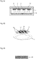
- the plate 8 is preferably supported horizontally by a support plate 11 as illustrated in FIGS. Figures 12 and 13 , which can be manipulated manually or by a robot.
- This support plate 11 is made of a material compatible with the oxidation treatment, for example quartz, silicon or silicon carbide.
- the wafer 8 is raised relative to the support wafer 11 by spacers 12 which support the wafer 8 in areas that do not contain components (especially between the components).
- the plate 8 is prevented from moving horizontally by retaining elements 13 cooperating with the periphery of the plate 8.
- the spacers 12 and the retaining elements 13 are of generally cylindrical shape.
- the support plate 11 are integral with the support plate 11, for example fixed to the support plate 11 by bayonet type links. They are made for example of quartz or silicon carbide, and may be in the same material or in different materials. In a preferred embodiment, the support plate 11 is made of silicon and the spacers and retaining elements 12, 13 are made of quartz. Such a support plate 11 with its spacers 12 and retaining elements 13 can also be used during the step of the figure 11 when this consists of a CVD or PVD deposition operation.
- the plate 8 is placed on the support plate 11 in a reversed position relative to the oxidation treatment of the figure 7 .
- the plate 8 is placed on the support plate 11 in a reversed position relative to the oxidation treatment of the figure 9 .
- the step of releasing the wafer 8 from the substrate 1 can be implemented by removing all the lower layer of silicon 3 and the entire intermediate layer of silicon oxide 4 by chemical etching or plasma etching. It is also possible to remove the lower layer of silicon 3 and the intermediate layer of silicon oxide 4 only on the back of the components or groups of components, the wafer 8 then keeping part of these layers 3, 4. However, these operations are long and expensive.
- the wafer 8 is formed by a portion of the upper layer of silicon 2 and its release from the substrate 1 is implemented as described below and illustrated in FIGS. Figures 14 and 15 .
- the etched substrate 1 is fixed as shown in FIG. figure 5 against a heating element 14 in a closed chamber 15 ( figure 14 ), the upper layer of silicon 2 being oriented downwards, the lower silicon layer 3, so oriented upwards, being against the heating element 14.
- the method of fixing the substrate 1 against the heating element 14 can be electrostatic (by application of an electric field) or mechanical.
- a solution of hydrofluoric acid (HF) is added to the chamber 15, out of contact with the substrate 1.
- the hydrofluoric acid vapors which then saturate the interior of the chamber 15 etch the intermediate layer of silicon oxide 4, without attacking the silicon.
- the heating element 14, regulated in temperature prevents the condensation of the water produced by the reaction between the hydrofluoric acid and the silicon oxide, which condensation would cause a bonding between the part to be released and the rest of the substrate 1.
- the part to be released namely the wafer 8 is defined beforehand by a kerf made during the etching of the upper layer of silicon 2 and which forms the periphery of the wafer 8.
- openings 16 for example hatch-shaped as represented at figure 15 , are etched in the wafer 8 around a central zone 17 comprising the components. These openings 16 allow the passage of hydrofluoric acid vapor.
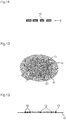
- the figure 15 shows an example of plate 8 having a shape consisting of rectangular or square parts. Other forms can of course be envisaged, for example the circular form.
- the watch components manufactured by the method according to the invention can have very precise dimensions and good surface conditions which will improve the operating accuracy and the efficiency of the mechanisms that will use them.
- the watch components would then have a composite structure comprising one or more intermediate layers of silicon oxide.
- the photoresist mask 5 which serves to structure the upper layer of silicon 2 ( figure 3 ) could be replaced by a silicon oxide mask.
- the substrate could be etched from both sides.
- the layer or layers of silicon oxides used to stop etching could be reinforced by one or more parylene layers.
- the present invention does not exclude the use of one or more metal layers to stop the etching.
Abstract
Le procédé selon l'invention comprend les étapes suivantes : a) se munir d'un substrat (1) comprenant une première couche de silicium (2), une deuxième couche de silicium (3) et, entre les deux, une couche intermédiaire d'oxyde de silicium (4) ; b) graver la première couche de silicium (2) afin d'y former les composants horlogers ; c) libérer du substrat (1) une plaquette (8) formée par au moins tout ou partie de la première couche de silicium (2) gravée et comprenant les composants horlogers ; d) oxyder thermiquement puis désoxyder les composants horlogers ; e) former par oxydation thermique ou dépôt une couche d'oxyde de silicium sur les composants horlogers ; f) détacher les composants horlogers de la plaquette (8).The method according to the invention comprises the following steps: a) providing a substrate (1) comprising a first silicon layer (2), a second silicon layer (3) and, in between, an intermediate layer of silicon silicon oxide (4); b) etching the first silicon layer (2) to form the watch components therein; c) releasing from the substrate (1) a wafer (8) formed by at least all or part of the first etched silicon layer (2) and comprising the watch components; d) thermally oxidizing and deoxidizing the watch components; e) forming by thermal oxidation or depositing a layer of silicon oxide on the watch components; f) detach the watch components from the plate (8).
Description
La présente invention porte sur un procédé de fabrication de composants horlogers, tels que des spiraux, des ancres, des roues, des aiguilles, des bascules, des leviers, des ressorts ou des balanciers, en silicium.The present invention relates to a method for manufacturing watch components, such as spirals, anchors, wheels, needles, rockers, levers, springs or pendulums, made of silicon.
Des procédés de fabrication de composants horlogers en silicium ont été décrits notamment dans les documents
La présente invention vise à proposer un procédé permettant de fabriquer des composants horlogers en silicium de grande qualité.The present invention aims to provide a method for manufacturing high quality silicon watch components.
A cette fin il est prévu un procédé selon la revendication 1 ou la revendication 2 et les revendications qui en dépendent.For this purpose there is provided a method according to
La présente invention propose en outre un organe de support qui facilite la mise en oeuvre de ce procédé et plus généralement la mise en oeuvre d'un traitement thermique d'une plaquette. Cet organe de support est défini dans la revendication 18 et les revendications qui en dépendent.The present invention further provides a support member which facilitates the implementation of this method and more generally the implementation of a thermal treatment of a wafer. This support member is defined in
D'autres caractéristiques et avantages de la présente invention apparaîtront à la lecture de la description détaillée suivante faite en référence aux dessins annexés dans lesquels :
- les
figures 1 à 11 montrent schématiquement des étapes successives d'un procédé selon un mode de réalisation particulier de l'invention ; - les
figures 12 et 13 sont respectivement une vue en perspective et une vue de profil d'un organe de support utilisé dans le procédé selon le mode de réalisation particulier de l'invention pour supporter une plaquette de silicium pendant un traitement d'oxydation thermique de cette dernière ; - les
figures 14 et 15 montrent schématiquement une étape du procédé selon le mode de réalisation particulier de l'invention, dans laquelle une plaquette de silicium gravée est libérée d'un substrat composite ; - la
figure 16 montre un substrat composite à partir duquel peut être mis en oeuvre un procédé selon un autre mode de réalisation de l'invention.
- the
Figures 1 to 11 show schematically successive steps of a method according to a particular embodiment of the invention; - the
Figures 12 and 13 are respectively a perspective view and a side view of a support member used in the method according to the particular embodiment of the invention for supporting a silicon wafer during a thermal oxidation treatment of the latter; - the
Figures 14 and 15 schematically show a step of the method according to the particular embodiment of the invention, in which an etched silicon wafer is released from a composite substrate; - the
figure 16 shows a composite substrate from which can be implemented a method according to another embodiment of the invention.
Un procédé de fabrication de composants horlogers en silicium, notamment pour montres-bracelets, comprend selon un mode de réalisation particulier de l'invention les étapes successives illustrées aux
A une première étape (
A une deuxième étape (
A une étape suivante (
Le masque de laque photosensible 5 est ensuite éliminé par gravure chimique ou gravure plasma (
A une étape suivante (
Puis la plaquette 8 est placée dans un four d'oxydation pour être soumise à un traitement thermique, typiquement entre 600°C et 1300°C, oxydant toute la surface extérieure des composants horlogers (
A ce stade du procédé, on peut mesurer des caractéristiques physiques des composants horlogers ou de certains d'entre eux, notamment leurs dimensions. Grâce à l'étape précédente d'oxydation - désoxydation, ces caractéristiques physiques sont bien définies et leur mesure peut donc être précise, n'étant pas perturbée par les défauts de surface. Dans le cas de spiraux, on peut déterminer leur raideur. Pour un spiral donné, la raideur peut être déterminée en couplant le spiral, alors qu'il est encore attaché à la plaquette 8 ou détaché de la plaquette 8, à un balancier d'inertie prédéterminée, en mesurant la fréquence de l'ensemble balancier-spiral et en déduisant de cette mesure, par calcul, la raideur du spiral. On peut plus particulièrement mettre en oeuvre le procédé décrit dans la demande de brevet
A encore une autre étape du procédé (
A une étape finale, les composants horlogers sont détachés de la structure de base de la plaquette 8.In a final step, the watch components are detached from the base structure of the
Durant les étapes d'oxydation (
De préférence, durant le traitement d'oxydation de la
L'étape de libération de la plaquette 8 du substrat 1 (
On fixe le substrat 1 gravé tel que montré à la
La partie à libérer, à savoir la plaquette 8, est définie préalablement par une saignée réalisée lors de la gravure de la couche supérieure de silicium 2 et qui forme le pourtour de la plaquette 8. Pendant cette même gravure de la couche supérieure de silicium 2, des ouvertures 16, par exemple en forme de hachures comme représenté à la
La
Les composants horlogers fabriqués par le procédé selon l'invention peuvent avoir des dimensions très précises et de bons états de surface qui amélioreront la précision de fonctionnement et le rendement des mécanismes qui les utiliseront.The watch components manufactured by the method according to the invention can have very precise dimensions and good surface conditions which will improve the operating accuracy and the efficiency of the mechanisms that will use them.
Des modifications du procédé selon l'invention tel que décrit ci-dessus sont bien entendu possibles.Modifications of the method according to the invention as described above are of course possible.
Par exemple, bien que les deux étapes d'oxydation - désoxydation (
On pourrait aussi partir d'un substrat double ou triple SOI, voire plus, c'est-à-dire d'un substrat comprenant plus de deux couches de silicium séparées par des couches intermédiaires d'oxyde de silicium, comme le substrat 20 montré à la
Le masque de laque photosensible 5 qui sert à structurer la couche supérieure de silicium 2 (
Dans d'autres variantes, on pourrait graver le substrat depuis ses deux faces.In other variants, the substrate could be etched from both sides.
La ou les couches d'oxydes de silicium servant à arrêter la gravure pourraient être renforcées par une ou des couches de type parylène.The layer or layers of silicon oxides used to stop etching could be reinforced by one or more parylene layers.
Enfin, la présente invention n'exclut pas non plus l'utilisation d'une ou plusieurs couches métalliques pour arrêter la gravure.Finally, the present invention does not exclude the use of one or more metal layers to stop the etching.
Claims (21)
Priority Applications (10)
| Application Number | Priority Date | Filing Date | Title |
|---|---|---|---|
| EP18162729.0A EP3543795A1 (en) | 2018-03-20 | 2018-03-20 | Method for manufacturing silicon clock components |
| US16/980,126 US11880165B2 (en) | 2018-03-20 | 2019-03-19 | Method for manufacturing silicon timepiece components |
| PCT/IB2019/052198 WO2019180596A1 (en) | 2018-03-20 | 2019-03-19 | Method for producing silicon watchmaking components |
| JP2020550771A JP2021518548A (en) | 2018-03-20 | 2019-03-19 | Manufacturing method of components for manufacturing silicon watches |
| EP21182494.1A EP3907567A1 (en) | 2018-03-20 | 2019-03-19 | Support member for thermal treatment of a plate |
| CN202210052591.1A CN114460826A (en) | 2018-03-20 | 2019-03-19 | Method for manufacturing silicon timepiece component |
| CN201980020156.7A CN111868637B (en) | 2018-03-20 | 2019-03-19 | Method for manufacturing silicon timepiece component |
| EP19717200.0A EP3769162B1 (en) | 2018-03-20 | 2019-03-19 | Method for manufacturing silicon clock components |
| JP2023146855A JP2023164549A (en) | 2018-03-20 | 2023-09-11 | Method for manufacturing component for manufacturing of silicon watch |
| US18/533,303 US20240103442A1 (en) | 2018-03-20 | 2023-12-08 | Support member for supporting a wafer during a heat treatment |
Applications Claiming Priority (1)
| Application Number | Priority Date | Filing Date | Title |
|---|---|---|---|
| EP18162729.0A EP3543795A1 (en) | 2018-03-20 | 2018-03-20 | Method for manufacturing silicon clock components |
Publications (1)
| Publication Number | Publication Date |
|---|---|
| EP3543795A1 true EP3543795A1 (en) | 2019-09-25 |
Family
ID=61691846
Family Applications (3)
| Application Number | Title | Priority Date | Filing Date |
|---|---|---|---|
| EP18162729.0A Withdrawn EP3543795A1 (en) | 2018-03-20 | 2018-03-20 | Method for manufacturing silicon clock components |
| EP19717200.0A Active EP3769162B1 (en) | 2018-03-20 | 2019-03-19 | Method for manufacturing silicon clock components |
| EP21182494.1A Pending EP3907567A1 (en) | 2018-03-20 | 2019-03-19 | Support member for thermal treatment of a plate |
Family Applications After (2)
| Application Number | Title | Priority Date | Filing Date |
|---|---|---|---|
| EP19717200.0A Active EP3769162B1 (en) | 2018-03-20 | 2019-03-19 | Method for manufacturing silicon clock components |
| EP21182494.1A Pending EP3907567A1 (en) | 2018-03-20 | 2019-03-19 | Support member for thermal treatment of a plate |
Country Status (5)
| Country | Link |
|---|---|
| US (2) | US11880165B2 (en) |
| EP (3) | EP3543795A1 (en) |
| JP (2) | JP2021518548A (en) |
| CN (2) | CN111868637B (en) |
| WO (1) | WO2019180596A1 (en) |
Cited By (3)
| Publication number | Priority date | Publication date | Assignee | Title |
|---|---|---|---|---|
| EP3882714A1 (en) * | 2020-03-19 | 2021-09-22 | Patek Philippe SA Genève | Method for manufacturing a silicon clock component |
| EP3882710A1 (en) * | 2020-03-19 | 2021-09-22 | Patek Philippe SA Genève | Method for manufacturing a silicon-based clock component |
| EP4227742A1 (en) | 2022-02-11 | 2023-08-16 | Sigatec SA | Method for manufacturing a silicon part |
Families Citing this family (7)
| Publication number | Priority date | Publication date | Assignee | Title |
|---|---|---|---|---|
| EP3543796A1 (en) * | 2018-03-21 | 2019-09-25 | Nivarox-FAR S.A. | Method for manufacturing a silicon hairspring |
| EP3839642A1 (en) | 2019-12-20 | 2021-06-23 | Patek Philippe SA Genève | Method for manufacturing timepiece springs and etching mask for such a method |
| EP3865954A1 (en) * | 2020-02-12 | 2021-08-18 | Nivarox-FAR S.A. | Method for manufacturing a device with flexible single-piece silicon sheets, for timepieces |
| EP3907565A1 (en) | 2020-05-07 | 2021-11-10 | Patek Philippe SA Genève | Method for manufacturing a silicon timepiece component |
| NL2028796B1 (en) | 2021-07-20 | 2023-01-23 | Flexous Mech Ip B V | Method of manufacturing a plurality of mechanical resonators in a manufacturing wafer |
| EP4212965A1 (en) | 2022-01-14 | 2023-07-19 | Richemont International S.A. | Method for limiting the deformation of a silicon timepiece |
| EP4312084A1 (en) | 2022-07-26 | 2024-01-31 | Nivarox-FAR S.A. | Method for manufacturing a silicon hairspring |
Citations (9)
| Publication number | Priority date | Publication date | Assignee | Title |
|---|---|---|---|---|
| US4400861A (en) * | 1981-11-27 | 1983-08-30 | Oyo Instruments, Inc. | Fabrication of seismic springs from sheets |
| EP0732635A1 (en) | 1995-03-17 | 1996-09-18 | C.S.E.M. Centre Suisse D'electronique Et De Microtechnique Sa | Micromechanical element and process for its manufacture |
| EP1422436A1 (en) | 2002-11-25 | 2004-05-26 | CSEM Centre Suisse d'Electronique et de Microtechnique SA | Spiral watch spring and its method of production |
| WO2010057777A1 (en) * | 2008-11-21 | 2010-05-27 | Nivarox-Far S.A. | Method for making a micromechanical part |
| EP2215531A1 (en) | 2007-11-28 | 2010-08-11 | Manufacture et fabrique de montres et chronomètres Ulysse Nardin Le Locle SA | Mechanical oscillator having an optimized thermoelastic coefficient |
| EP2799940A1 (en) * | 2013-04-30 | 2014-11-05 | The Swatch Group Management Services AG | Packaging for hands of watches |
| EP2799939A1 (en) * | 2013-04-30 | 2014-11-05 | Universo S.A. | Support for the treatment of micromechanical parts |
| WO2016128694A1 (en) * | 2015-02-13 | 2016-08-18 | Tronic's Microsystems | Mechanical oscillator and associated production method |
| EP3181938A1 (en) | 2015-12-18 | 2017-06-21 | CSEM Centre Suisse d'Electronique et de Microtechnique SA - Recherche et Développement | Method for manufacturing a hairspring with a predetermined stiffness by removing material |
Family Cites Families (30)
| Publication number | Priority date | Publication date | Assignee | Title |
|---|---|---|---|---|
| JP2000074227A (en) | 1998-08-26 | 2000-03-14 | Sony Corp | Vacuum processing device and magnetic seal rotary bearing unit |
| US6706202B1 (en) * | 2000-09-28 | 2004-03-16 | Xerox Corporation | Method for shaped optical MEMS components with stressed thin films |
| JP2002341054A (en) * | 2001-05-11 | 2002-11-27 | Seiko Instruments Inc | Hair spring, its structural body, and speed governing mechanism and timepiece using it |
| SG112005A1 (en) | 2003-12-29 | 2005-06-29 | Sony Corp | A surface treatment for use in the fabrication of mems devices |
| TWI258208B (en) * | 2004-01-14 | 2006-07-11 | Mosel Vitelic Inc | Loading device for wafer and the supporting structure thereof |
| CH696881A5 (en) * | 2005-06-28 | 2008-01-15 | Eta Sa Mft Horlogere Suisse | micro-mechanical part reinforced silicon and its manufacturing process. |
| US7573022B2 (en) | 2005-07-27 | 2009-08-11 | The Regents Of The University Of California | Method for fabricating vertically-offset interdigitated comb actuator device |
| US8614110B1 (en) * | 2006-07-25 | 2013-12-24 | The United States Of America As Represented By The Secretary Of The Navy | Method for fabricating a dual-crystalline silicon suspension system using pre-fabricated cavities |
| CH714952B1 (en) * | 2007-05-08 | 2019-10-31 | Patek Philippe Sa Geneve | Watchmaking component, its method of manufacture and application of this method. |
| US8030133B2 (en) * | 2008-03-28 | 2011-10-04 | Icemos Technology Ltd. | Method of fabricating a bonded wafer substrate for use in MEMS structures |
| CH701499B1 (en) | 2009-07-23 | 2016-09-15 | Montres Breguet Sa | A method of manufacturing a micromechanical part reinforced silicon. |
| EP2561409B1 (en) | 2010-04-21 | 2019-08-28 | Team Smartfish GmbH | Element of regulation for a timepiece and a corresponding process |
| EP2423764B1 (en) | 2010-08-31 | 2013-03-27 | Rolex S.A. | Device for measuring the torque of a hairspring |
| EP2472340B1 (en) | 2011-01-03 | 2021-03-03 | Patek Philippe SA Genève | Timepiece component and method for manufacturing same |
| WO2013045706A2 (en) * | 2011-09-29 | 2013-04-04 | Rolex S.A. | Integral assembly of a hairspring and a collet |
| US9034754B2 (en) * | 2012-05-25 | 2015-05-19 | LuxVue Technology Corporation | Method of forming a micro device transfer head with silicon electrode |
| JP2014168819A (en) | 2013-03-01 | 2014-09-18 | Nippon Telegr & Teleph Corp <Ntt> | Production method of micromechanical structure |
| CA2930570A1 (en) * | 2013-11-13 | 2015-05-21 | Michigan Technological University | Silicon nanowire-based sensor arrays |
| WO2015113973A1 (en) | 2014-01-29 | 2015-08-06 | Cartier Création Studio Sa | Thermally compensated hairspring made from ceramic comprising silicon in the composition of same and method for adjusting same |
| JP6486697B2 (en) | 2014-02-26 | 2019-03-20 | シチズン時計株式会社 | Hairspring manufacturing method and hairspring |
| JP2015179013A (en) | 2014-03-19 | 2015-10-08 | シチズンホールディングス株式会社 | Manufacturing method of balance spring |
| EP2937311B1 (en) | 2014-04-25 | 2019-08-21 | Rolex Sa | Method for manufacturing a reinforced timepiece component, corresponding timepiece component and timepiece |
| JP2016133495A (en) | 2015-01-22 | 2016-07-25 | シチズンホールディングス株式会社 | Method of manufacturing timepiece component and timepiece component |
| JP2016161394A (en) | 2015-03-02 | 2016-09-05 | シチズンホールディングス株式会社 | Timepiece component |
| JP2016173355A (en) | 2015-03-16 | 2016-09-29 | シチズンホールディングス株式会社 | Manufacturing method of machine component |
| JP6554328B2 (en) | 2015-05-29 | 2019-07-31 | 株式会社Screenホールディングス | Heat treatment equipment |
| EP3109199B1 (en) * | 2015-06-25 | 2022-05-11 | Nivarox-FAR S.A. | Silicon-based part with at least one chamfer and method for manufacturing same |
| EP3109200B1 (en) * | 2015-06-25 | 2023-06-28 | Nivarox-FAR S.A. | Micromechanical part with reduced contact surface and method for manufacturing same |
| US10072892B2 (en) | 2015-10-26 | 2018-09-11 | Globalwafers Co., Ltd. | Semiconductor wafer support ring for heat treatment |
| TWI796444B (en) | 2018-03-20 | 2023-03-21 | 瑞士商百達翡麗日內瓦股份有限公司 | Method for manufacturing timepiece thermocompensated hairsprings of precise stiffness |
-
2018
- 2018-03-20 EP EP18162729.0A patent/EP3543795A1/en not_active Withdrawn
-
2019
- 2019-03-19 EP EP19717200.0A patent/EP3769162B1/en active Active
- 2019-03-19 US US16/980,126 patent/US11880165B2/en active Active
- 2019-03-19 CN CN201980020156.7A patent/CN111868637B/en active Active
- 2019-03-19 WO PCT/IB2019/052198 patent/WO2019180596A1/en unknown
- 2019-03-19 EP EP21182494.1A patent/EP3907567A1/en active Pending
- 2019-03-19 JP JP2020550771A patent/JP2021518548A/en active Pending
- 2019-03-19 CN CN202210052591.1A patent/CN114460826A/en active Pending
-
2023
- 2023-09-11 JP JP2023146855A patent/JP2023164549A/en active Pending
- 2023-12-08 US US18/533,303 patent/US20240103442A1/en active Pending
Patent Citations (10)
| Publication number | Priority date | Publication date | Assignee | Title |
|---|---|---|---|---|
| US4400861A (en) * | 1981-11-27 | 1983-08-30 | Oyo Instruments, Inc. | Fabrication of seismic springs from sheets |
| EP0732635A1 (en) | 1995-03-17 | 1996-09-18 | C.S.E.M. Centre Suisse D'electronique Et De Microtechnique Sa | Micromechanical element and process for its manufacture |
| EP1422436A1 (en) | 2002-11-25 | 2004-05-26 | CSEM Centre Suisse d'Electronique et de Microtechnique SA | Spiral watch spring and its method of production |
| EP2215531A1 (en) | 2007-11-28 | 2010-08-11 | Manufacture et fabrique de montres et chronomètres Ulysse Nardin Le Locle SA | Mechanical oscillator having an optimized thermoelastic coefficient |
| WO2010057777A1 (en) * | 2008-11-21 | 2010-05-27 | Nivarox-Far S.A. | Method for making a micromechanical part |
| EP2799940A1 (en) * | 2013-04-30 | 2014-11-05 | The Swatch Group Management Services AG | Packaging for hands of watches |
| EP2799939A1 (en) * | 2013-04-30 | 2014-11-05 | Universo S.A. | Support for the treatment of micromechanical parts |
| WO2016128694A1 (en) * | 2015-02-13 | 2016-08-18 | Tronic's Microsystems | Mechanical oscillator and associated production method |
| EP3181938A1 (en) | 2015-12-18 | 2017-06-21 | CSEM Centre Suisse d'Electronique et de Microtechnique SA - Recherche et Développement | Method for manufacturing a hairspring with a predetermined stiffness by removing material |
| EP3181938B1 (en) | 2015-12-18 | 2019-02-20 | CSEM Centre Suisse d'Electronique et de Microtechnique SA - Recherche et Développement | Method for manufacturing a hairspring with a predetermined stiffness by removing material |
Non-Patent Citations (4)
| Title |
|---|
| "MEMS For Watches", 2004, pages 1 - 4, XP010767811 |
| "Sidewall Smoothing of Bosch Scallops via Thermal Oxidation", 7 June 2012 (2012-06-07), XP055699858 |
| LAURA MCCREDDIE-DOAK: "This is where Patek Philippe develops the watches of the future", 31 December 2017 (2017-12-31), XP055699852, Retrieved from the Internet <URL:https://www.wired.co.uk/article/patek-philippes-aquanaut-travel-time-is-packed-with-innovation> |
| SYLVIAN AUBRY: "THÉORIE DES ÉCHAPPEMENTS", July 2016, article "5.2 Gravure profonde du silicium (DRIE)", pages: 287 - 292, XP055699856 |
Cited By (5)
| Publication number | Priority date | Publication date | Assignee | Title |
|---|---|---|---|---|
| EP3882714A1 (en) * | 2020-03-19 | 2021-09-22 | Patek Philippe SA Genève | Method for manufacturing a silicon clock component |
| EP3882710A1 (en) * | 2020-03-19 | 2021-09-22 | Patek Philippe SA Genève | Method for manufacturing a silicon-based clock component |
| WO2021186332A1 (en) * | 2020-03-19 | 2021-09-23 | Patek Philippe Sa Geneve | Method for manufacturing a silicon-based timepiece component |
| WO2021186333A1 (en) * | 2020-03-19 | 2021-09-23 | Patek Philippe Sa Geneve | Method for manufacturing a timepiece component made of silicon |
| EP4227742A1 (en) | 2022-02-11 | 2023-08-16 | Sigatec SA | Method for manufacturing a silicon part |
Also Published As
| Publication number | Publication date |
|---|---|
| JP2021518548A (en) | 2021-08-02 |
| WO2019180596A1 (en) | 2019-09-26 |
| EP3907567A1 (en) | 2021-11-10 |
| US20240103442A1 (en) | 2024-03-28 |
| CN111868637A (en) | 2020-10-30 |
| EP3769162B1 (en) | 2022-08-10 |
| US11880165B2 (en) | 2024-01-23 |
| US20210026299A1 (en) | 2021-01-28 |
| JP2023164549A (en) | 2023-11-10 |
| CN114460826A (en) | 2022-05-10 |
| CN111868637B (en) | 2022-04-12 |
| EP3769162A1 (en) | 2021-01-27 |
Similar Documents
| Publication | Publication Date | Title |
|---|---|---|
| EP3769162B1 (en) | Method for manufacturing silicon clock components | |
| EP3769161B1 (en) | Method for manufacturing thermocompensated hairsprings with precise stiffness | |
| WO2015113973A1 (en) | Thermally compensated hairspring made from ceramic comprising silicon in the composition of same and method for adjusting same | |
| EP3543796A1 (en) | Method for manufacturing a silicon hairspring | |
| CH713151A2 (en) | Flexible blade for watchmaking, and method of manufacture. | |
| EP3845770B1 (en) | Method for manufacturing timepiece hairsprings | |
| EP3495894B1 (en) | Method for manufacturing a clock component | |
| EP3789825B1 (en) | Method for manufacturing a plurality of microparts | |
| CH714806B1 (en) | Process for manufacturing silicon watch components. | |
| EP1121622A1 (en) | Structure for reflection lithography mask and method for making same | |
| CH714815A2 (en) | Process for manufacturing a silicon spiral for watchmaking | |
| EP3865954A1 (en) | Method for manufacturing a device with flexible single-piece silicon sheets, for timepieces | |
| FR3073082B1 (en) | METHOD FOR MANUFACTURING A FILM ON A CARRIER HAVING A NON-PLANAR SURFACE | |
| CH717124A2 (en) | A method of manufacturing a device with one-piece flexible silicon blades, in particular for watchmaking. | |
| FR3073083A1 (en) | METHOD FOR MANUFACTURING A FILM ON A FLEXIBLE SHEET | |
| EP4111264A1 (en) | Silicon timepiece component for a timepiece | |
| EP3882714A1 (en) | Method for manufacturing a silicon clock component | |
| EP3907565A1 (en) | Method for manufacturing a silicon timepiece component | |
| EP4303668A1 (en) | Device for determining the stiffness of a spiral | |
| EP4283408A1 (en) | Method for manufacturing a clock component | |
| CH719712A2 (en) | Process for manufacturing a watch component. | |
| WO2021186332A1 (en) | Method for manufacturing a silicon-based timepiece component | |
| EP2579105A2 (en) | Method for manufacturing a timepiece | |
| CH711960B1 (en) | A method of manufacturing a hairspring of predetermined stiffness with removal of material |
Legal Events
| Date | Code | Title | Description |
|---|---|---|---|
| PUAI | Public reference made under article 153(3) epc to a published international application that has entered the european phase |
Free format text: ORIGINAL CODE: 0009012 |
|
| AK | Designated contracting states |
Kind code of ref document: A1 Designated state(s): AL AT BE BG CH CY CZ DE DK EE ES FI FR GB GR HR HU IE IS IT LI LT LU LV MC MK MT NL NO PL PT RO RS SE SI SK SM TR |
|
| AX | Request for extension of the european patent |
Extension state: BA ME |
|
| TPAC | Observations filed by third parties |
Free format text: ORIGINAL CODE: EPIDOSNTIPA |
|
| STAA | Information on the status of an ep patent application or granted ep patent |
Free format text: STATUS: THE APPLICATION IS DEEMED TO BE WITHDRAWN |
|
| 18D | Application deemed to be withdrawn |
Effective date: 20200603 |