EP3767329B1 - Vorrichtung mit analogen verzögerungsschaltungen für die ultraschallbildgebung - Google Patents
Vorrichtung mit analogen verzögerungsschaltungen für die ultraschallbildgebung Download PDFInfo
- Publication number
- EP3767329B1 EP3767329B1 EP20185004.7A EP20185004A EP3767329B1 EP 3767329 B1 EP3767329 B1 EP 3767329B1 EP 20185004 A EP20185004 A EP 20185004A EP 3767329 B1 EP3767329 B1 EP 3767329B1
- Authority
- EP
- European Patent Office
- Prior art keywords
- delay circuit
- analog delay
- signal
- reflected
- capacitors
- Prior art date
- Legal status (The legal status is an assumption and is not a legal conclusion. Google has not performed a legal analysis and makes no representation as to the accuracy of the status listed.)
- Active
Links
- 238000012285 ultrasound imaging Methods 0.000 title 1
- 239000003990 capacitor Substances 0.000 claims description 307
- 238000002604 ultrasonography Methods 0.000 claims description 250
- 239000000523 sample Substances 0.000 claims description 89
- 230000003111 delayed effect Effects 0.000 claims description 53
- 230000000737 periodic effect Effects 0.000 claims description 45
- 230000001934 delay Effects 0.000 claims description 34
- 230000005540 biological transmission Effects 0.000 description 57
- 238000012545 processing Methods 0.000 description 50
- 238000012986 modification Methods 0.000 description 48
- 230000004048 modification Effects 0.000 description 48
- 238000010586 diagram Methods 0.000 description 34
- 238000000034 method Methods 0.000 description 26
- 239000000872 buffer Substances 0.000 description 20
- 238000005070 sampling Methods 0.000 description 15
- 230000002401 inhibitory effect Effects 0.000 description 6
- 238000004458 analytical method Methods 0.000 description 3
- 238000003384 imaging method Methods 0.000 description 3
- 230000003213 activating effect Effects 0.000 description 2
- 230000001174 ascending effect Effects 0.000 description 2
- 230000017531 blood circulation Effects 0.000 description 2
- 239000006185 dispersion Substances 0.000 description 2
- 230000000694 effects Effects 0.000 description 2
- 230000003321 amplification Effects 0.000 description 1
- 239000002872 contrast media Substances 0.000 description 1
- 238000013461 design Methods 0.000 description 1
- 238000001514 detection method Methods 0.000 description 1
- 238000002592 echocardiography Methods 0.000 description 1
- 230000002526 effect on cardiovascular system Effects 0.000 description 1
- 239000000284 extract Substances 0.000 description 1
- 230000006870 function Effects 0.000 description 1
- 238000003199 nucleic acid amplification method Methods 0.000 description 1
- 230000003287 optical effect Effects 0.000 description 1
- 230000003071 parasitic effect Effects 0.000 description 1
- 239000004065 semiconductor Substances 0.000 description 1
Images


Classifications
-
- G—PHYSICS
- G01—MEASURING; TESTING
- G01S—RADIO DIRECTION-FINDING; RADIO NAVIGATION; DETERMINING DISTANCE OR VELOCITY BY USE OF RADIO WAVES; LOCATING OR PRESENCE-DETECTING BY USE OF THE REFLECTION OR RERADIATION OF RADIO WAVES; ANALOGOUS ARRANGEMENTS USING OTHER WAVES
- G01S7/00—Details of systems according to groups G01S13/00, G01S15/00, G01S17/00
- G01S7/52—Details of systems according to groups G01S13/00, G01S15/00, G01S17/00 of systems according to group G01S15/00
- G01S7/52017—Details of systems according to groups G01S13/00, G01S15/00, G01S17/00 of systems according to group G01S15/00 particularly adapted to short-range imaging
- G01S7/52023—Details of receivers
- G01S7/52025—Details of receivers for pulse systems
- G01S7/52026—Extracting wanted echo signals
-
- A—HUMAN NECESSITIES
- A61—MEDICAL OR VETERINARY SCIENCE; HYGIENE
- A61B—DIAGNOSIS; SURGERY; IDENTIFICATION
- A61B8/00—Diagnosis using ultrasonic, sonic or infrasonic waves
- A61B8/52—Devices using data or image processing specially adapted for diagnosis using ultrasonic, sonic or infrasonic waves
- A61B8/5215—Devices using data or image processing specially adapted for diagnosis using ultrasonic, sonic or infrasonic waves involving processing of medical diagnostic data
- A61B8/5238—Devices using data or image processing specially adapted for diagnosis using ultrasonic, sonic or infrasonic waves involving processing of medical diagnostic data for combining image data of patient, e.g. merging several images from different acquisition modes into one image
- A61B8/5246—Devices using data or image processing specially adapted for diagnosis using ultrasonic, sonic or infrasonic waves involving processing of medical diagnostic data for combining image data of patient, e.g. merging several images from different acquisition modes into one image combining images from the same or different imaging techniques, e.g. color Doppler and B-mode
-
- A—HUMAN NECESSITIES
- A61—MEDICAL OR VETERINARY SCIENCE; HYGIENE
- A61B—DIAGNOSIS; SURGERY; IDENTIFICATION
- A61B8/00—Diagnosis using ultrasonic, sonic or infrasonic waves
- A61B8/52—Devices using data or image processing specially adapted for diagnosis using ultrasonic, sonic or infrasonic waves
- A61B8/5269—Devices using data or image processing specially adapted for diagnosis using ultrasonic, sonic or infrasonic waves involving detection or reduction of artifacts
-
- A—HUMAN NECESSITIES
- A61—MEDICAL OR VETERINARY SCIENCE; HYGIENE
- A61B—DIAGNOSIS; SURGERY; IDENTIFICATION
- A61B8/00—Diagnosis using ultrasonic, sonic or infrasonic waves
- A61B8/54—Control of the diagnostic device
-
- G—PHYSICS
- G01—MEASURING; TESTING
- G01S—RADIO DIRECTION-FINDING; RADIO NAVIGATION; DETERMINING DISTANCE OR VELOCITY BY USE OF RADIO WAVES; LOCATING OR PRESENCE-DETECTING BY USE OF THE REFLECTION OR RERADIATION OF RADIO WAVES; ANALOGOUS ARRANGEMENTS USING OTHER WAVES
- G01S15/00—Systems using the reflection or reradiation of acoustic waves, e.g. sonar systems
- G01S15/88—Sonar systems specially adapted for specific applications
- G01S15/89—Sonar systems specially adapted for specific applications for mapping or imaging
- G01S15/8906—Short-range imaging systems; Acoustic microscope systems using pulse-echo techniques
- G01S15/8909—Short-range imaging systems; Acoustic microscope systems using pulse-echo techniques using a static transducer configuration
- G01S15/8915—Short-range imaging systems; Acoustic microscope systems using pulse-echo techniques using a static transducer configuration using a transducer array
-
- G—PHYSICS
- G01—MEASURING; TESTING
- G01S—RADIO DIRECTION-FINDING; RADIO NAVIGATION; DETERMINING DISTANCE OR VELOCITY BY USE OF RADIO WAVES; LOCATING OR PRESENCE-DETECTING BY USE OF THE REFLECTION OR RERADIATION OF RADIO WAVES; ANALOGOUS ARRANGEMENTS USING OTHER WAVES
- G01S7/00—Details of systems according to groups G01S13/00, G01S15/00, G01S17/00
- G01S7/52—Details of systems according to groups G01S13/00, G01S15/00, G01S17/00 of systems according to group G01S15/00
- G01S7/52017—Details of systems according to groups G01S13/00, G01S15/00, G01S17/00 of systems according to group G01S15/00 particularly adapted to short-range imaging
- G01S7/52019—Details of transmitters
- G01S7/5202—Details of transmitters for pulse systems
-
- G—PHYSICS
- G01—MEASURING; TESTING
- G01S—RADIO DIRECTION-FINDING; RADIO NAVIGATION; DETERMINING DISTANCE OR VELOCITY BY USE OF RADIO WAVES; LOCATING OR PRESENCE-DETECTING BY USE OF THE REFLECTION OR RERADIATION OF RADIO WAVES; ANALOGOUS ARRANGEMENTS USING OTHER WAVES
- G01S7/00—Details of systems according to groups G01S13/00, G01S15/00, G01S17/00
- G01S7/52—Details of systems according to groups G01S13/00, G01S15/00, G01S17/00 of systems according to group G01S15/00
- G01S7/52017—Details of systems according to groups G01S13/00, G01S15/00, G01S17/00 of systems according to group G01S15/00 particularly adapted to short-range imaging
- G01S7/52046—Techniques for image enhancement involving transmitter or receiver
- G01S7/52047—Techniques for image enhancement involving transmitter or receiver for elimination of side lobes or of grating lobes; for increasing resolving power
-
- G—PHYSICS
- G10—MUSICAL INSTRUMENTS; ACOUSTICS
- G10K—SOUND-PRODUCING DEVICES; METHODS OR DEVICES FOR PROTECTING AGAINST, OR FOR DAMPING, NOISE OR OTHER ACOUSTIC WAVES IN GENERAL; ACOUSTICS NOT OTHERWISE PROVIDED FOR
- G10K11/00—Methods or devices for transmitting, conducting or directing sound in general; Methods or devices for protecting against, or for damping, noise or other acoustic waves in general
- G10K11/18—Methods or devices for transmitting, conducting or directing sound
- G10K11/26—Sound-focusing or directing, e.g. scanning
- G10K11/34—Sound-focusing or directing, e.g. scanning using electrical steering of transducer arrays, e.g. beam steering
- G10K11/341—Circuits therefor
- G10K11/346—Circuits therefor using phase variation
Definitions
- An embodiment relates to an apparatus.
- an ultrasound diagnostic apparatus that generates ultrasound image data representing an ultrasound image obtained by imaging an internal condition of a subject with an ultrasound probe including a delay circuit (analog delay circuit) that performs delay processing on a reflected-wave signal using an analog system.
- a delay circuit analog delay circuit
- Patent Application US2019/008477A1 discloses cancelling periodic noise superimposed on echo signals by subtracting a cancelling signal output without transmitting a wave.
- An apparatus provided according to an aspect of the present invention comprises a first delay circuit that delays an ultrasound signal in a first channel using a plurality of capacitors, a second delay circuit that delays an ultrasound signal in a second channel using a plurality of capacitors, and a control unit that makes a first write start position in which writing the ultrasound signal in the plurality of capacitors in the first delay circuit is started and a second write start position in which writing the ultrasound signal in the plurality of second capacitors in the second delay circuit is started different from each other.
- the control unit makes the first write start position and the second write start position different from each other such that a phase difference between a waveform which represents periodic noise that is superimposed on the ultrasound signal that is delayed by the first delay circuit and a waveform which represents periodic noise that is superimposed on the ultrasound signal that is delayed by the second delay circuit is 180 degrees.
- the control unit may make the first write start position and the second write start position different from each other based on the number of capacitors contained in the first delay circuit or the second delay circuit.
- the apparatus may further comprise a third delay circuit that delays an ultrasound signal in a third channel using a plurality of capacitors, and a fourth delay circuit that delays an ultrasound signal in a fourth channel using a plurality of capacitors.
- the control unit may make the first write start position, the second write start position, a third write start position in which writing the ultrasound signal in the capacitor in the third delay circuit is started, and a fourth write start position in which writing the ultrasound signal in the capacitor in the fourth delay circuit is started different from one another such that a phase difference between a waveform which represents periodic noise that is superimposed on the ultrasound signal that is delayed by the third delay circuit and a waveform which represents periodic noise that is superimposed on the ultrasound signal that is delayed by the fourth delay circuit is 180 degrees and a phase difference between the waveform which represents periodic noise that is superimposed on the ultrasound signal that is delayed by the first delay circuit and the waveform which represents periodic noise that is superimposed on the ultrasound signal that is delayed by the third delay circuit and a phase difference between the waveform which represents periodic noise that is superimposed on the
- the control unit may perform control such that write start positions in each channel are different from each other based on types of noise components that are contained in a frequency band of the ultrasound probe.
- the apparatus may further comprise a summing unit that generates a summing signal by summing the ultrasound signal that is delayed by the first delay circuit and the ultrasound signal that is delayed by the second delay circuit.
- the apparatus may further comprise a summing unit that generates a summing signal by summing (A)signal generated by summing the ultrasound signal that is delayed by the first delay circuit and the ultrasound signal that is delayed by the second delay circuit and (B)signal generated by summing the ultrasound signal that is delayed by the third delay circuit and the ultrasound signal that is delayed by the fourth delay circuit.
- A summing signal generated by summing the ultrasound signal that is delayed by the first delay circuit and the ultrasound signal that is delayed by the second delay circuit
- B signal generated by summing the ultrasound signal that is delayed by the third delay circuit and the ultrasound signal that is delayed by the fourth delay circuit.
- the first delay circuit may periodically write the ultrasound signal in the capacitor of the first delay circuit
- the second delay circuit may periodically write the ultrasound signal in the capacitor of the second delay circuit
- the first delay circuit may periodically read the ultrasound signal from the capacitor of the first delay circuit
- the second delay circuit may periodically read the ultrasound signal from the capacitor of the second delay circuit
- the first delay circuit may periodically write the ultrasound signal in the capacitor of the first delay circuit
- the second delay circuit may periodically write the ultrasound signal in the capacitor of the second delay circuit
- the third delay circuit may periodically write the ultrasound signal in the capacitor of the third delay circuit
- the fourth delay circuit may periodically write the ultrasound signal in the capacitor of the fourth delay circuit.
- the first delay circuit may periodically read the ultrasound signal from the capacitor of the first delay circuit
- the second delay circuit may periodically read the ultrasound signal from the capacitor of the second delay circuit
- the third delay circuit may periodically read the ultrasound signal from the capacitor of the third delay circuit
- the fourth delay circuit may periodically read the ultrasound signal from the capacitor of the fourth delay circuit.
- the number of the capacitors that are used by the first delay circuit and the number of the capacitors that are used by the second delay circuit may be equal to each other.
- the apparatus may be an ultrasound probe.
- the apparatus may be an ultrasound diagnostic apparatus.
- the apparatus may further comprise a display control unit that causes a display unit to display an ultrasound image based on the ultrasound signal that is delayed by the first delay circuit and the ultrasound signal that is delayed by the second delay circuit.
- the apparatus may further comprise a display control unit that causes a display unit to display an ultrasound image based on the ultrasound signal that is delayed by the first delay circuit, the ultrasound signal that is delayed by the second delay circuit, the ultrasound signal that is delayed by the third delay circuit, and the ultrasound signal that is delayed by the fourth delay circuit.
- a display control unit that causes a display unit to display an ultrasound image based on the ultrasound signal that is delayed by the first delay circuit, the ultrasound signal that is delayed by the second delay circuit, the ultrasound signal that is delayed by the third delay circuit, and the ultrasound signal that is delayed by the fourth delay circuit.
- the control unit may make a first read position in which the ultrasound signal is read from the capacitor of the first delay circuit and a second read position in which the ultrasound signal is read from the capacitor of the second delay circuit at identical times different from each other by making the first write start position and the second write start position different from each other.
- the control unit may make the first write start position and the second write start position different from each other based on a delay of the first delay circuit and a delay of the second delay circuit.
- the control unit may make the first write start position, the second write start position, the third write start position, and the fourth write start position different from one another based on a delay of the first delay circuit, a delay of the second delay circuit, a delay of the third delay circuit, and a delay of the fourth delay circuit.
- the apparatus may further comprise 2 N ("N" is a natural number) delay circuits that include the first delay circuit and the second delay circuit and each of which delays an ultrasound signal using a plurality of capacitors.
- Each of the first channel and the second channel may correspond to a single transducer.
- Writing the ultrasound signal in the capacitor may be performed by turning on switch connected between a input terminal and the capacitor.
- Reading the ultrasound signal from the capacitor may be performed by turning on switch connected between the capacitor and a output terminal.
- the first delay circuit may delay a signal in the first channel from an ultrasound transducer.
- the first delay circuit may comprise a plurality of switched capacitors connected in parallel.
- Each of the switched capacitors may comprise a capacitor and a write switch.
- the write switch may connect the capacitor of a switched capacitor to the first channel.
- the first delay circuit may be adapted to sample the signal from the first channel at different positions along its waveform by activating the write switches of the switched capacitors at different times.
- the second delay circuit may delay a signal in the second channel from an ultrasound transducer.
- the second delay circuit may comprise a plurality of switched capacitors connected in parallel.
- Each of the switched capacitors may comprise a capacitor and a write switch.
- the write switch may connect the capacitor of a switched capacitor to the second channel.
- the second delay circuit may be adapted to sample the signal from the second channel at different positions along its waveform by activating the write switches of the switched capacitors at different times.
- the control unit may start sampling the signal from the first channel in the first delay circuit and start sampling the signal from the second channel in the second delay circuit at different positions in the respective delay circuits.
- the first and second delay circuits may have equal number of switched capacitors.
- An apparatus includes a first delay circuit, a second delay circuit, and processing circuitry.
- the first delay circuit delays an ultrasound signal in a first channel using a plurality of capacitors.
- the second delay circuit delays an ultrasound signal in a second channel using a plurality of capacitors.
- the processing circuitry make a first write start position in which writing the ultrasound signal in the capacitor in the first delay circuit is started and a second write start position in which writing the ultrasound signal in the capacitor in the second delay circuit is started different from each other.
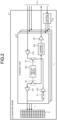
- FIG. 1 is a diagram for describing an example of a configuration of an ultrasound diagnostic apparatus 100 according to the embodiment.
- the ultrasound diagnostic apparatus 100 according to the embodiment includes an ultrasound probe 1, a display 2, an input device 3, and an apparatus main unit 10.
- the ultrasound diagnostic apparatus 100 is an example of an apparatus.
- the ultrasound probe 1 is detachably connected to the apparatus main unit 10.
- the transmitted ultrasound is reflected sequentially on a surface with acoustic impedance discontinuity.
- the reflected ultrasound is received by the ultrasound probe 1 as reflected waves (echoes).
- the reflected waves are converted into reflected-wave signals in the ultrasound probe 1.
- the amplitude of the reflected-wave signals depends on the difference in acoustic impedance on the discontinuity surface on which ultrasound is reflected. Reflected-wave signals in the case where transmitted ultrasound pulses are reflected on a moving blood flow, a heart wall, or the like, undergo a frequency shift because of the Doppler effect depending on velocity components of a mobile object with respect to the direction in which ultrasound is transmitted.
- the reflected-wave signals are then converted into a summing signal to be described below in the ultrasound probe 1 and the summing signal is then output.
- the ultrasound probe 1 may be of a convex type or a sector type, and various types of ultrasound probes are usable as the ultrasound probe 1.
- the ultrasound probe 1 includes a plurality of transducers 21 (refer to FIG. 2 ) to be described below.
- the transducers 21 are arranged two-dimensionally in a lateral direction and an elevation direction and are divided into multiple subarrays.
- the subarrays for example, refer to respective groups into each of which a given number of transducers 21 are grouped.
- One subarray includes the given number of transducers 21.
- the ultrasound probe 1 is an example of the apparatus. A configuration of the ultrasound probe 1 will be described below.
- the display 2 displays a graphical user interface (GUI) for a user of the ultrasound diagnostic apparatus 100 to input various types of setting requests using the input device 3 and displays an ultrasound image that is represented by ultrasound image data that is generated in the apparatus main unit 10, etc.
- GUI graphical user interface
- the display 2 is an example of a display unit.
- the input device 3 is implemented using a track ball, a switch, a dial, a touch command screen, a footswitch, a joystick, or the like.
- the input device 3 receives the various setting requests from the user of the ultrasound diagnostic apparatus 100 and transfers the received various setting requests to the apparatus main unit 10.
- the input device 3 receives various setting requests for controlling the ultrasound probe 1 and transfers the various setting requests to the apparatus main unit 10.
- the apparatus main unit 10 controls transmission of ultrasound performed by the ultrasound probe 1 and reception of reflected waves performed by the ultrasound probe 1.
- the apparatus main unit 10 generates an ultrasound image based on the summing signal that is transmitted from the ultrasound probe 1 and to be described below.
- the apparatus main unit 10 includes transmitter-receiver circuitry 11, B-mode processing circuitry 12, Doppler processing circuitry 13, image generation circuitry 14, storage circuitry 15, and control circuitry 16.
- the transmitter-receiver circuitry 11 transmits and receives various types of data, etc., to and from the ultrasound probe 1 and the apparatus main unit 10. For example, the transmitter-receiver circuitry 11 repeatedly generates a transmission pulse (rate pulse) for forming transmission ultrasound at a given rate frequency (pulse repetition frequency (PRF)) and transmits the generated transmission pulses to the ultrasound probe 1.
- a transmission pulse rate pulse
- PRF pulse repetition frequency
- the transmitter-receiver circuitry 11 transmits, to the ultrasound probe 1, a delay (transmission delay) to ultrasound that is transmitted from the ultrasound probe 1. Specifically, the transmitter-receiver circuitry 11 transmits a transmission delay to ultrasound that is output (transmitted) by each transducer 21.
- the transmitter-receiver circuitry 11 transmits, to the ultrasound probe 1, a delay (a reception delay) to a reflected-wave signal. Specifically, the transmitter-receiver circuitry 11 transmits, to the ultrasound probe 1, a reception delay to a reflected-wave signal that is transmitted by each transducer 21.
- the transmitter-receiver circuitry 11 includes an A/D (Analog to Digital) converter and a receiving beamformer.
- A/D Analog to Digital
- the receiving beamformer performs a phasing and summing processing on the digital summing signal of each subarray, thereby generates reflected-wave data.
- the receiving beamformer transmits the generated reflected-wave data to the B-mode processing circuitry 12 and the Doppler processing circuitry 13.
- the B-mode processing circuitry 12 receives the reflected-wave data that is output from the transmitter-receiver circuitry 11.
- the B-mode processing circuitry 12 performs logarithmic amplification, envelope detection, etc., on the received reflected-wave data, thereby generating data (B-mode data) in which the signal intensity is expressed by the intensity of illuminance.
- the B-mode processing circuitry 12 is, for example, implemented using a processor.
- the Doppler processing circuitry 13 receives the reflected-wave data that is output from the transmitter-receiver circuitry 11. The Doppler processing circuitry 13 then performs frequency analysis on rate information from the received reflected-wave data, extracts blood flows, tissue and contrast agent echo components resulting from the Doppler effect, and generates data (Doppler data) obtained by extracting mobile object information, such as an average rate, dispersion, power, etc., with respect to a large number of points.
- the Doppler processing circuitry 13, for example, is implemented using the processor.
- the image generation circuitry 14 generates ultrasound image data from the sets of data that are generated by the B-mode processing circuitry 12 ad the Doppler processing circuitry 13. In other words, the image generation circuitry 14 generates B-mode image data in which the echo intensity is represented by the luminance from the B-mode data that is generated by the B-mode processing circuitry 12. From the Doppler data that is generated by the Doppler processing circuitry 13, the image generation circuitry 14 generates color Doppler image data serving as an average rate image, a dispersion image or a power image representing the mobile object information or an image of a combination of the images.
- the image generation circuitry 14 is implemented using, for example, the processor.
- the storage circuitry 15 is implemented using, for example, a random access memory (RAM), a semiconductor memory device, such as a flash memory, a hard disk, or an optical disk.
- the storage circuitry 15 stores ultrasound image data that is generated by the image generation circuitry 14.
- the storage circuitry 15 may store the data that is generated by the B-mode processing circuitry 12 and the Doppler processing circuitry 13.
- the storage circuitry 15 stores various types of data, such as control programs for performing ultrasound transmission and reception, image processing and display processing, diagnostic information (for example, patient IDs and observations of a doctor), a diagnostic protocol and various types of body marks.
- the storage circuitry 15 stores elements for calculating the above-described various delays (transmission delays and reception delays). For example, sets of coordinates each representing the position of each of the transducers 21 a and sets of coordinates each representing the position of focal point are taken as such elements.
- the control circuitry 16 controls the whole process performed by the ultrasound diagnostic apparatus 100. For example, according to the various setting requests that are input by an operator via the input device 3 and various control programs and various types of data that are read from the storage circuitry 15, the control circuitry 16 controls the processing performed by the transmitter-receiver circuitry 11, the B-mode processing circuitry 12, the Doppler processing circuitry 13 and the image generation circuitry 14.
- the control circuitry 16 controls the display 2 such that the display 2 displays the ultrasound image data that is stored in the storage circuitry 15 and the various types of image data that are stored in the storage circuitry 15, a GUI for performing the processing by the image generation circuitry 14 and the result of processing performed by the image generation circuitry 14, or the like.
- control circuitry 16 controls the display 2 such that the display 2 displays the ultrasound image that is represented by the ultrasound image data obtained from the summing signal to be described below. In other words, the control circuitry 16 controls the display 2 such that the display 2 displays the ultrasound image based on the summing signal.
- the control circuitry 16 is an example of a display controller or a display control unit.
- the control circuitry 16 controls the transmitter-receiver circuitry 11 such that the transmitter-receiver circuitry 11 transmits the transmission delay for each channel and the reception delay of each channel to the ultrasound probe 1.
- one channel is assigned to one transducer 21.
- the control circuitry 16 reads, from the storage circuitry 15, the elements for calculating the various delays that are stored in the storage circuitry 15 and, based on the read elements, calculates the above-described various delays of the respective transducers 21, that is, the respective channels.
- the control circuitry 16 controls the transmitter-receiver circuitry 11 such that the transmitter-receiver circuitry 11 transmits the various delays of the respective channels to the ultrasound probe 1.
- the control circuitry 16 is implemented using, for example, the processor.
- FIG. 2 is a diagram for describing the example of the configuration of the ultrasound probe 1 according to the embodiment.
- the ultrasound probe 1 includes the transducers 21, a plurality of subarray units 22, and control circuitry 23.
- the apparatus main unit 10 may include the subarray units 22 and the control circuitry 23.
- the apparatus main unit 10 may include only the control circuitry 23 among the subarray units 22 and the control circuitry 23.
- the transducers 21 are arranged two-dimensionally in the lateral direction and the elevation direction and are divided into the multiple subarrays.
- the control circuitry 23 sets transmission delays of the respective transducers 21 and each of the transducers 21 transmits ultrasound based on a drive signal at the timing corresponding to the corresponding transmission delay to the subject P.
- One subarray unit 22 is arranged for one subarray.
- Each of the subarray units 22 includes a buffer 22a, an analog delay circuit 22b, a pulser 22c, a preamplifier 22d, summing circuitry 22e, a buffer 22f, and switches S1, S2 and S3.
- the buffers 22a, the analog delay circuits 22b, the pulsers 22c, the preamplifiers 22d, and the switches S1, S2 and S3 corresponding in number to the channels forming the subarray are present in each of the subarray units 22.
- the buffer 22a, the analog delay circuit 22b, the pulser 22c, the preamplifier 22d, and the switches S1, S2 and S3 are arranged for each channel.
- the buffer 22a, the analog delay circuit 22b, the pulser 22c, the preamplifier 22d, and the switches S1, S2 and S3 are arranged for each of the transducers 21.
- one summing circuitry 22e and one buffer 22f are arranged in each subarray unit 22.
- one summing circuitry 22e and one buffer 22f are arranged in one subarray.
- One control circuitry 23 is arranged in the ultrasound probe 1.
- the buffer 22a, the analog delay circuit 22b, the pulser 22c, the preamplifier 22d, the summing circuitry 22e, the buffer 22f, and the switches S1, S2 and S3 are arranged on at least one application specific integrated circuit (ASIC) that the ultrasound probe 1 includes and that is not illustrated in the drawings.
- ASIC application specific integrated circuit
- the buffer 22a is connected to the transmitter-receiver circuitry 11 and the switch S3.
- the transmitter-receiver circuitry 11 transmits transmission pulses to the analog delay circuits 22b via the buffer 22a.
- the analog delay circuit 22b is implemented using an analog circuit.
- the analog delay circuit 22b is connected to the switch S2 and the switch S3.
- the analog delay circuit 22b includes a plurality of switched capacitors.
- the switched capacitor for example, has a function of a memory device and temporarily stores an ultrasound signal.
- the ultrasound signal that is input to the switched capacitors is, for example, a transmission pulse that is transmitted from the transmitter-receiver circuitry 11 of the apparatus main unit 10 or a reflected-wave signal that is transmitted from the preamplifier 22d.
- the analog delay circuit 22b executes the delay processing to delay the ultrasound signal using the switched capacitors. In other words, the analog delay circuit 22b assigns delays to the ultrasound signal using the switched capacitors.
- the analog delay circuit 22b executes delay processing of assigning a delay for each transducer 21 (channel) necessary to focus the ultrasound that is generated from the transducer 21 into a beam and determine transmission directivity to a transmission pulse that is supplied from the apparatus main unit 10. For example, under the control of the control circuitry 23, the analog delay circuit 22b assigns a delay that is set for each channel to a transmission pulse for each channel that is output from the apparatus main unit 10. The analog delay circuit 22b transmits the transmission pulse assigned with the delay to the pulser 22c via the switch S2.
- the analog delay circuit 22b executes delay processing of assigning a delay necessary to determine reception directivity to a reflected-wave signal that is transmitted from the preamplifier 22d.
- the analog delay circuit 22b transmits the reflected-wave signal assigned with the delay to the summing circuitry 22e via the switch S2.
- the analog delay circuit is an example of a delay circuit.
- the pulser 22c is connected to the switch S2 and is connected to the transducer 21. Under the control of the control circuitry 23, the pulser 22c generates a drive signal of a given amplitude. For example, the pulser 22c generates a drive signal based on a transmission pulse that is transmitted from the analog delay circuit 22b and transmits the generated drive signal to the transducer 21.
- the preamplifier 22d is connected to the switch S1 and the switch S3. On receiving a reflected-wave signal that is transmitted from the transducer 21 via the switch S1, the preamplifier 22d amplifies the received reflected-wave signal by a gain that is set previously. The preamplifier 22d transmits the amplified reflected-wave signal to the analog delay circuit 22b via the switch S3.
- the summing circuitry 22e is connected to the switch S2 and the buffer 22f.
- the summing circuitry 22e executes a summing process of summing a plurality of reflected-wave signals on which the delay processing has been performed and that are transmitted from the analog delay circuits 22b corresponding respectively to a plurality of channels forming one subarray.
- the summing circuitry 22e transmits one signal (summing signal) obtained by summing the reflected-wave signals by performing the summing processing to the transmitter-receiver circuitry 11.
- the summing circuitry 22e is an example of a summing unit.
- the summing signal is an example of an ultrasound signal.
- the buffer 22f outputs the summing signal that is transmitted from the summing circuitry 22e to the transmitter-receiver circuitry 11.
- the summing circuitry 22e transmits the summing signal to the transmitter-receiver circuitry 11 via the buffer 22f.
- the switch S1 is turned off to prevent a signal with a wide amplitude that is generated by the pulser 22c from being input to the preamplifier 22d.
- the switch S1 When a reflected-wave signal that is transmitted from the transducer 21 is supplied to the preamplifier 22d, the switch S1 is turned on. In other words, when reflected waves are received, the switch S1 connects the transducer 21 and the preamplifier 22d.
- the switch S2 selectively switches the destination to which an ultrasound signal that is transmitted from the analog delay circuit 22b is transmitted to any one of the pulser 22c and the summing circuitry 22e. For example, when ultrasound is transmitted, the switch S2 switches a destination to which a transmission pulse assigned with a delay is transmitted to the pulser 22c. In other words, when ultrasound is transmitted, the switch S2 connects the analog delay circuit 22b and the pulser 22c. When reflected waves are received, the switch S2 switches a destination to which a reflected-wave signal assigned with a delay is transmitted to the summing circuitry 22e. In other words, when reflected waves are received, the switch S2 connects the analog delay circuit 22b and the summing circuitry 22e.
- the switch S3 selectively switches a source from which an ultrasound signal to be input to the analog delay circuit 22b is transmitted to any one of the buffer 22a and the preamplifier 22d. For example, when ultrasound is transmitted, the switch S3 connects the analog delay circuit 22b and the buffer 22a such that a transmission pulse that is transmitted from the transmitter-receiver circuitry 11 is input to the analog delay circuit 22b. When reflected waves are received, the switch S3 connects the analog delay circuit 22b and the preamplifier 22d such that a reflected-wave signal that is transmitted from the preamplifier 22d is input to the analog delay circuit 22b.
- the switch S2 and the switch S3 are arranged to share the analog delay circuit 22b between transmission and reception.
- the analog delay circuit 22b may be divided into an analog delay circuit for transmission and an analog delay circuit for reception.
- the switch S2 and the switch S3 need not be arranged in the ultrasound probe 1.
- the control circuitry 23 controls the buffers 22a, the analog delay circuits 22b, the pulsers 22c, the preamplifiers 22d, the summing circuitry 22e, the buffer 22f, and the switches S1, S2 and S3.
- the buffer 22a, the analog delay circuit 22b, the pulser 22c, the preamplifier 22d, the summing circuitry 22e, the buffer 22f, and the switches S1, S2 and S3 are sometimes referred to as control subjects below.
- the control circuitry 23 controls each control subject such that each control subject performs the above-described operations.
- the control circuitry 23 controls the respective control subjects by transmitting various control signals respectively to the control subjects.
- control circuitry 23 generates, for the respective channels, various control signals corresponding to the channels and to be supplied to the analog delay circuits 22b.
- An example of a method of generating various control signals performed by the control circuitry 23 will be described.
- the control circuitry 23 receives transmission delays corresponding to the respective channels from the transmitter-receiver circuitry 11 of the apparatus main unit 10. Based on the transmission delays, the control circuitry 23 generates control signals for causing transmission pulses that are input to the analog delay circuits 22b to be output from the analog delay circuit 22b after the transmission delays.
- the control circuitry 23 transmits the generated control signals to the analog delay circuits 22b.
- the control circuitry 23 receives reception delays corresponding respectively to channels from the transmitter-receiver circuitry 11 of the apparatus main unit 10. Based on the reception delays, the control circuitry 23 generates control signals for causing reflected-wave signals that are input to the analog delay circuits 22b to be output from the analog delay circuits 22b after the reception delays. The control circuitry 23 transmits the generated control signals to the analog delay circuits 22b.
- the control circuitry 23 is implemented using, for example, the processor.
- the control circuitry 23 is an example of a controller or a control unit.
- FIG. 3 is a diagram for describing the example of the configuration of the analog delay circuit 22b according to the embodiment.
- the analog delay circuit 22b illustrated in FIG. 3 samples parts of a transmission pulse, which is input, in a given sampling period and stores each of the parts of the transmission pulse at multiple sampling time points.
- the analog delay circuit 22b sequentially reads the respective parts of the transmission pulse that are sampled and stored at sets of timing corresponding to the respective transmission delays and transmits the parts of the transmission pulse as a continuous transmission pulse again to the pulser 22c.
- the analog delay circuit 22b samples parts of a reflected-wave signal, which is input, in a given sampling period and stores each of the parts of the transmission pulse at multiple sampling time points.
- the analog delay circuit 22b sequentially reads the respective parts of the reflected-wave signal that are sampled and stored at sets of timing corresponding to the respective reception delays and transmits the parts of the reflected-wave signal as the continuous reflected-wave signal again to the summing circuitry 22e.
- the analog delay circuit 22b includes a plurality of switched capacitors SC_1 to SC_n (n is a natural number that is 2 or larger), an input terminal 43, and an output terminal 44.
- One end of the write switch 40_k is connected to the input terminal 43.
- the input terminal 43 is connected to the switch S3. As schematically represented by an arrow 50, a transmission pulse that is transmitted from the transmitter-receiver circuitry 11 and a reflected-wave signal that is transmitted from the preamplifier 22d are input to the input terminal 43.
- the other end of the write switch 40_k is connected to one end of the capacitor 41_k.
- the other end of the capacitor 41_k is grounded.
- One end of the read switch 42_k is connected to the one end of the capacitor 41_k.
- the other end of the read switch 42_k is connected to the output terminal 44.
- the output terminal 44 is connected to the switch S2. As schematically represented by an arrow 51, the delayed transmission pulse and the delayed reflected-wave signal are output from the output terminal 44 to the switch S2.
- the write switch 40_k includes a control signal input terminal 45_k.
- the control signal input terminal 45_k is connected to the control circuitry 23.
- a control signal for writing (write control signal) is input from the control circuitry 23 to the control signal input terminal 45_k.
- the write control signal will be described below.
- the write switches 40_1 to 40_n respectively sample parts of transmission pulse that are input according to write control signals.
- the write switches 40_1 to 40_n write the respective sampled parts of the transmission pulse in the capacitors 41_1 to 41_n, respectively. Accordingly, the capacitors 41_1 to 41_n store the sampled parts of the transmission pulse, respectively.
- the switches 40_1 to 40_n respectively sample parts of reflected-wave signal, which is input, according to write control signals.
- the write switches 40_1 to 40_n write the sampled parts of the reflected-wave signal in the capacitors 41_1 to 41_n, respectively. Accordingly, the capacitors 41_1 to 41_n respectively store the sampled parts of the reflected-wave signal, respectively.
- the read switch 42_k includes a control signal input terminal 46_k.
- the control signal input terminal 46_k is connected to the control circuitry 23.
- a control signal for reading (read control signal) is input from the control circuitry 23 to the control signal input terminal 46_k.
- the read control signal will be described below.
- the respective read switches 42_1 to 42_n respectively read the parts of the transmission pulse that are written (stored) in the respective capacitors 41_1 to 41_n according to the read control signals.
- the read switches 42_1 to 42_n sequentially output the respective read parts of the transmission pulse, thereby outputting the continuous transmission pulse.
- the respective read switches 42_1 to 42_n respectively read the parts of the reflected-wave signal that are written in the respective capacitors 41_1 to 41_n according to the read control signals.
- the read switches 42_1 to 42_n sequentially output the respective read parts of the reflected-wave signal, thereby outputting the continuous reflected-wave signal.
- FIG. 4 is a diagram illustrating an example of a plurality of write control signals 47_1 to 47_n and a plurality of read control signals 48_1 to 48_n.
- a write control signal 47_k is input to a control signal input terminal 45_k.
- a write switch 40_k enables conduction between the input terminal 43 and the capacitor 41_k during a period in which the write control signal 47_k represents on (high level). In other words, the write switch 40_k electrically connects the input terminal 43 and the capacitor 41_k. For example, the period in which the write control signal 47_k represents on coincides with the period of one clock of a system clock of the ultrasound diagnostic apparatus 100.
- the write switch 40_k electrically disconnects the input terminal 43 and the capacitor 41_k during the period in which the write control signal 47_k represents off (low level).
- the capacitor 41_k accumulates charges during the period in which the write control signal 47_k represents on.
- the capacitor 41_k samples part of a transmission pulse that is input to the input terminal 43 corresponding to the period in which the write control signal 47_k represents on and stores the sampled part of the transmission pulse.
- the capacitor 41_k samples part of a reflected-wave signal that is input to the input terminal 43 corresponding to the period in which the write control signal 47_k represents on and stores the sampled part of the reflected-wave signal.
- the state in which on is represented sequentially switches over the write control signals 47_1 to 47_n approximately successively.
- parts of the transmission pulse are sampled in the given sampling period and are stored in the capacitors 41_1 to 41_n, respectively.
- parts of the reflected-wave signal are sampled in the given sampling period and are stored in the capacitors 41_n to 41_n, respectively.
- the write control signals 47_1 to 47_n enter the state in which on is represented in a given period T1. After the write control signal 47_n enters the state in which on is represented, the write control signal 47_1 again enters the state in which on is represented. The state in which on is represented sequentially switches over the write control signals 47_1 to 47_n approximately successively.
- parts of the transmission pulse that are sampled at a plurality of sampling time points after the time point at which the part of the transmission pulse that is stored in the capacitor 41_n is sampled are overwritten again in the capacitors 41_1 to 41_n sequentially from the capacitor 41_1 to the capacitor 41_n and are stored.
- parts of the reflected-wave signal that are sampled at a plurality of sampling time points after the time point at which the part of the reflected-wave signal that is stored in the capacitor 41_n is sampled are overwritten again in the capacitors 41_1 to 41_n sequentially from the capacitor 41_1 to the capacitor 41_n and are stored.
- the analog delay circuit 22b periodically writes an ultrasound signal in the capacitors of the analog delay circuit 22b.
- a read control signal 48_k is input to a control signal input terminal 46_k.
- the read switch 42_k enables conduction between the output terminal 44 and a capacitor 41_k during a period in which a read control signal 48_k represents on.
- the read switch 42_k electrically connects the output terminal 44 and the capacitor 41_k.
- the period in which the read control signal 48_k represents on coincides with the period of one clock of the above-described system clock.
- the read switch 42_k electrically disconnects the output terminal 44 and the capacitor 41_k during the period in which a read control signal 48_k represents off.
- the capacitor 41_k emits charges during the period in which the read control signal 48_k represents on.
- the read switch 42_k reads the part of the transmission pulse that is stored in the capacitor 41_k and outputs the read part of the transmission pulse from the output terminal 44.
- the read switch 42_k reads the part of the reflected-wave signal that is stored in the capacitor 41_k and outputs the read part of the reflected-wave signal from the output terminal 44.
- the capacitor 41_k keeps storing the part of the stored transmission pulse or the stored part of the reflected-wave signal during the period in which the read control signal 48_k represents off.
- the state in which on is represented appears a delay T2 behind the state of the write control signal 47_k in which on is represented.
- the delay T2 is the above-described transmission delay when the transmission pulse is delayed.
- the delay T2 is the above-described reception delay when a reflected-wave signal is delayed. Accordingly, the part of the transmission pulse, or the part of the reflected-wave signal, that is stored in the capacitor 41_k is read after the delay T2 after being stored in the capacitor 41_k.
- the delay T2 is a value unique to each channel and thus is a value unique to each analog delay circuit 22b.
- the state in which on is represented sequentially switches over the read control signals 48_1 to 48_n approximately successively.
- the sampled parts of the transmission pulse are read from the capacitors 41_n to 41_n, respectively.
- the sampled parts of the reflected-wave signal are read from the capacitors 41_n to 41_n, respectively.
- the read control signals 48_1 to 48_n enter the state in which on is represented in the given period T1. After the read control signal 48_n enters the state in which on is represented, the read control signals 48_1 again enters the state in which on is represented. The state in which on is represented sequentially switches over the read control signals 48_1 to 48_n approximately successively.
- the parts of the transmission pulse that are sampled at the sampling time points after the sampling time point at which the part of the transmission pulse that is stored in the capacitor 41_n is sampled are read from the capacitor 41_1 to 41_n sequentially from the capacitors 41_1 to 41_n again.
- the parts of the reflected-wave signal that are sampled at the sampling time points after the sampling time point at which the part of the reflected-wave signal that is read from the capacitor 41_n is sampled are read from the capacitors 41_1 to 41_n sequentially from the capacitor 41_1 to 41_n again. In the analog delay circuit 22b, such read operations are repeated.
- the analog delay circuit 22b periodically reads an ultrasound signal from the capacitors of the analog delay circuit 22b.
- the above-described period T1 is a value corresponding to the number of the capacitors 41_1 to 41_n.
- the number of the capacitors 41_1 to 41_n is a value corresponding to the maximum delay in the delay processing that is performed by the analog delay circuit 22b.
- a write control signal 47_k and a read control signal 48_k have periodicity in which the state in which on is represented recurs every period T1. Because of such periodicity of the write control signal 47_k and the read control signal 48_k, a frequency component (spurious emission) that is not intended in design is superimposed onto the reflected-wave signal as a noise component. Such noise is also referred to as periodic noise.
- the period of the periodic noise (noise period) is the period T1.
- the periodic noise is superimposed onto the reflected-wave signals and thus the periodic noise is also superimposed onto the summing signal.
- noise components are superimposed onto the reflected-wave signals that are output from the analog delay circuits 22b and the summing signal that is output from the summing circuitry 22e.
- noise components result in a virtual image on an ultrasound image.
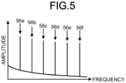
- FIG. 5 is a diagram for describing an example of the noise components that are superimposed onto a reflected-wave signal.
- FIG. 5 represents the result of frequency analysis on the reflected-wave signal.
- the horizontal axis represents the frequency and the vertical axis represents the amplitude.
- the component of a fundamental frequency (1/T1) represented by an arrow 56a contains a noise component.
- the components of multiples of the fundamental frequency ((2/T1), (3/T1), (3/T1), (4/T1), (5/T1) and (6/T1)) contain noise components.
- the component of the fundamental frequency (1/T1) is also referred to as a fundamental wave component.
- the component of twice the fundamental frequency (2/T1), the component of three times the fundamental frequency (3/T1), the component of four times the fundamental frequency (4/T1), the component of five times the fundamental frequency (5/T1), and the component of six times the fundamental frequency (6/T1) are also respectively referred to as a second harmonic component, a third harmonic component, a fourth harmonic component, a fifth harmonic component, and a sixth harmonic component.
- the component of seven times the fundamental frequency (7/T1) contains a noise component.
- the component of seven times the fundamental frequency is also referred to as a seventh harmonic component.
- the fundamental wave component, the third harmonic component, the fifth harmonic component, and the seventh harmonic component are also referred to as odd harmonic components.
- the second harmonic component, the fourth harmonic component, and the sixth harmonic component are also referred to as even harmonic components.
- FIG. 6 is a diagram schematically illustrating the analog delay circuit 22b in the case where the number of the switch capacitors SC_1 to SC_n is 5.
- FIG. 7 is diagram illustrating an example of a pattern of the periodic noise that is superimposed onto the output signals that are output respectively from the switched capacitors SC_1 to SC_5.
- the length of an interconnect connecting the input terminal 43 and a switched capacitor SC_m is a length corresponding to the position of the switched capacitor SC_m.
- L1_m the length of the interconnect connecting the input terminal 43 and the switched capacitor SC_m
- L1_m the length of the interconnect connecting the input terminal 43 and the switched capacitor SC_m
- the length of an interconnect connecting the output terminal 44 and the switched capacitor SC_m is a length corresponding to the position of the switched capacitor SC_m.
- L2_m the length of the interconnect connecting the output terminal 44 and the switched capacitor SC_m
- L2_1 the length of the interconnect connecting the output terminal 44 and the switched capacitor SC_m
- L2_3 the circuit layout of the analog delay circuit 22b
- the parasitic impedance differs in each switched capacitor SC_m.
- the length of an interconnect connecting the control circuitry 23 and the switched capacitor SC_m is a length corresponding to the position of the switched capacitor SC_m.
- the length of the interconnect connecting the control circuitry 23 and the switched capacitor SC_m is denoted by "L3_m”, “L3_1”, “L3_2”, “L3_3”, “L3_4" and “L3_5" are different from one another.
- the rate of rise and the rate of decrease in the waveform of the control signal that is input differ in each switched capacitor SC_m.
- the degree of feedthrough differs in each switched capacitor SC_m.
- part of the control sigla is superimposed as noise on the output signal that is output from the switched capacitor SC_m and the degree of noise differs in each switched capacitor SC_m.
- the pattern of periodic noise that is superimposed onto the output signal that is output from the switched capacitor SC_m is denoted by "P_m", as illustrated in FIG. 7 , a pattern P_1, a pattern P_2, a pattern P_3, a pattern P_4, and a pattern P_5 are different from one another.
- the set of the patterns P_1 to P_5 appears repeatedly.
- the noise period is equal to the sampling period.
- the frequency of noise is not problematic because the noise frequency is out of the frequency band of the ultrasound probe 1; however, when the waveform of the noise that is superimposed in each switched capacitor SC_m differs, as illustrated in FIG. 7 , the periodic noise that is noise with the periodicity of the period T1 is superimposed onto the reflected-wave signal 60 that is output from the analog delay circuit 22b.
- the noise frequency is within the ultrasound frequency band and thus is problematic.
- FIG. 8 is a diagram for describing an example of processing to reduce the periodic noise.
- FIG. 8 illustrates a reflected-wave signal 200, a cancellation signal 201 and an image signal 202.
- Periodic noise 200a is superimposed onto the reflected-wave signal 200.
- the cancellation signal 201 is a reflected-wave signal that a transducer of the ultrasound probe outputs without transmitting ultrasound.
- the cancellation signal 201 is a reflected-wave signal not containing any reflected-wave of ultrasound from the subject.
- Periodic noise 201a is superimposed onto the cancellation signal 201.
- the receiver of the transmitter-receiver circuitry subtracts the cancellation signal 201 from the reflected-wave signal 200, thereby calculating the image signal 202 that is used for imaging.
- the periodic noise 200a that is superimposed onto the reflected-wave signal 200 is reduced in the image signal 202. As described above, the periodic noise is reduced in the image signal 202.
- the reflected-wave signal 200 and the cancellation signal 201 When one image signal 202 is generated, subtraction processing using two signals (the reflected-wave signal 200 and the cancellation signal 201) is performed. For example, when the number of signals to be added or subtracted is "s", the volume of random noise other than the periodic noise resulting from periodicity is proportional to "s 1/2 ". In the case where the periodic noise is reduced according to the above-described method, when using one reflected-wave signal 200 as the image signal 202 to be used for imaging is taken as a reference, the volume of random noise is multiplied by "2 1/2 " and increases.
- the ultrasound probe 1 executes processing to be described below to reduce the noise that is contained in the summing signal while inhibiting the frame rate from lowering.
- FIG. 9 is a diagram for describing an example of processing that the control circuitry 23 executes according to the embodiment.
- the control circuitry 23 determines two channels in a pair from the channels of the same subarray. In the following description, two channels in a pair are sometimes referred to as a pair channel.
- the control circuitry 23 determines a set of any two channels of the channels in the same subarray as a pair channel.
- the control circuitry 23 may determine one pair channel from multiple channels in the same subarray or may determine as many as pair channels. In other words, the control circuitry 23 determines at least one pair channel in each subarray.
- the control circuitry 23 performs processing to be described below on each pair channel.
- the control circuitry 23 controls read positions such that the read position in the analog delay circuit 22b corresponding to one of the channels of a pair channel and the read position of the analog delay circuit 22b corresponding to the other channel at an identical time are shifted from each other by a half period (T1/2) of a noise period T1.
- T1/2 half period of a noise period
- each of the analog delay circuits 22b_1 and 22b_2 illustrated in FIG. 9 includes 12 switched capacitors SC_1 to SC_12.
- the twelve switched capacitors SC_1 to SC_12 are sometimes simply referred to as "switched capacitors SC" when the switched capacitors SC_1 to SC_12 are not distinguished from one another.
- the above-described "read position" refers to a stitched capacitor SC in which the reflected-wave signal is read.
- the number of the switched capacitors SC is not limited to 12 and it may be any number. All the switched capacitors SC contained in the analog delay circuit 22b need not necessarily be used and, for example, only part of the switched capacitors SC_1 to SC_12, such as the switched capacitors SC_1 to SC_6, may be used.
- the 12 switched capacitors SC correspond to the noise period T1 and the six switched capacitors SC correspond to the half period (T1/2) of the noise period T1.
- the switched capacitors SC that are half as many as all the switched capacitors that are used in one analog delay circuit 22b correspond to the half period (T1/2) of the noise period T1.
- the control circuitry 23 makes the read position in which the reflected-wave signal is read from one of the capacitors 41_1 to 41_12 of the analog delay circuit 22b_1 and the read position in which the reflected-wave signal is read from one of the capacitors 41_1 to 41_12 of the analog delay circuit 22b_2 at identical times different from each other.
- the read position in which the reflected-wave signal is read from one of the capacitors 41_1 to 41_12 of the analog delay circuit 22b_1 is an example of the first read position.
- the read position in which the reflected-wave signal is read from one of the capacitors 41_1 to 41_12 of the analog delay circuit 22b_2 is an example of the second read position.
- control circuitry 23 controls the read positions such that, as schematically represented by an arrow 61, the read position in the analog delay circuit 22b_1 is the switched capacitor SC_1 of the analog delay circuit 22b_1 at a time T0.
- the control circuitry 23 controls the read positions such that the read position in the analog delay circuit 22b_2 is the switched capacitor SC_7 of the analog delay circuit 22b_2 at the time T0.
- the switched capacitor SC_7 of the analog delay circuit 22b_2 corresponds to the switched capacitor SC that is shifted by six switched capacitors SC from the switched capacitor SC_1.
- a read control signal 48_k that is input to a switched capacitor SC_k of the analog delay circuit 22b_1 is denoted by "48_k_1”.
- a read control signal 48_k that is input to a switched capacitor SC_k of the analog delay circuit 22b_2 is denoted by "48_k_2”.
- a read control signal 48_1_1 turns from the state in which off is represented into the state in which on is represented.
- the state in which on is represented sequentially switches over a plurality of read control signals 48_1_1 to 48_12_1 approximately successively.
- the parts of the reflected-wave signal that are sequentially read by the switched capacitors SC_1 to SC_12 of the analog delay circuit 22b_1 are output and accordingly the continuous reflected-wave signal is output from the analog delay circuit 22b_1.
- the analog delay circuit 22b_1 delays the reflected-wave signal in the channel corresponding to the analog delay circuit 22b_1 using the capacitors 41_1 to 41_n.
- the analog delay circuit 22b_1 is an example of the first delay circuit.
- the channel corresponding to the analog delay circuit 22b_1 is an example of the first channel.
- the reflected-wave signal is an example of the ultrasound signal.
- a read control signal 48_7_2 turns from the state in which off is represented into the state in which on is represented.
- the state in which on is represented switches sequentially over a plurality of read control signals 48_7_2 to 48_12_2 and 48_1_2 to 48_6_2 approximately successively.
- the parts of the reflected-wave signal that are sequentially read by the switched capacitors SC_7 to SC_12 and SC_1 to SC_6 of the analog delay circuit 22b_2 are output and accordingly the continuous reflected-wave signal is output from the analog delay circuit 22b_2.
- the analog delay circuit 22b_2 delays the reflected-wave signal in the channel corresponding to the analog delay circuit 22b_2 using the capacitors 41_1 to 41_n.
- the analog delay circuit 22b_2 is an example of the second delay circuit.
- the channel corresponding to the analog delay circuit 22b_2 is an example of the second channel.
- the number of the capacitors 41_n to 41_n that are used by the analog delay circuit 22b_1 and the number of the capacitors 41_1 to 41_n that are used by the analog delay circuit 22b_2 are equal to each other.
- FIG. 9 illustrates a waveform 63 representing a phase of the periodic noise of the period T1 that is superimposed on the reflected-wave signal that is output from the analog delay circuit 22b_1.
- FIG. 9 further illustrates a waveform 64 representing a phase of the periodic noise of the period T1 that is superimposed on the reflected-wave signal that is output from the analog delay circuit 22b_2.
- the waveform 63 is also a waveform representing the phase of the reflected-wave signal that is output from the analog delay circuit 22b_1.
- the waveform 64 is also a waveform representing the phase of the reflected-wave signal that is output from the analog delay circuit 22b_2.
- the waveform 63 and the waveform 64 are, for example, sine waves.
- phase difference the shift between the phase of the waveform 63 and the phase of the waveform 64 (phase difference) is 180 degrees at an identical time.
- the reason why the phase difference is 180 degrees is that the read position in the analog delay circuit 22b_1 at a given time T and the read position in the analog delay circuit 22b_2 at the time T are shifted from each other by the half period (T1/2) of the noise period T1.
- the phase difference is 180 degrees as described above and accordingly the reflected-wave signal that is output from the analog delay circuit 22b_1 and the reflected-wave signal that is output from the analog delay circuit 22b_2 are summed by the summing circuitry 22e, so that an adding signal in which the periodic noise is cancelled is obtained.
- the ultrasound probe 1 it is possible to obtain a summing signal in which periodic noise is reduced.
- the ultrasound probe 1 according to the embodiment uses the reflected-wave signals without using the above-described cancellation signal 201. For this reason, according to the ultrasound probe 1 according to the embodiment, when the case illustrated in FIG. 8 is taken as a reference, ultrasound image data is obtained without extra subtraction and thus random noise is not increased.
- the summing circuitry 22e simultaneously performs beamforming and noise cancellation. Accordingly, in the ultrasound probe 1 according to the embodiment, when ultrasound image data is generated, the subtraction processing using the cancellation signal 201 described above with reference to FIG. 8 need not be performed. For this reason, according to the ultrasound probe 1 according to the embodiment, compared to the case illustrated in FIG. 8 , the transmitting-receiving operation is performed only once to obtain ultrasound image data of one rate and it is thus possible to inhibit the frame rate from lowering.
- the ultrasound probe 1 it is possible to reduce noise contained in an adding signal while inhibiting the frame rate from lowering.
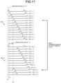
- a write start position refers to a switched capacitor SC in which writing a reflected-wave signal is started at a write start time (for example, the time T3 to be described below in FIG. 11 ).
- control circuitry 23 controls the write start positions in consideration of a difference between the reception delay corresponding to the analog delay circuit 22b_1 and the reception delay corresponding to the analog delay circuit 22b_2 (delay difference). An example of the control on the write start positions performed by the control circuitry 23 will be described.
- the reception delay is represented by the number of system clocks.
- the actual reception delay corresponds to the time of "r” clocks of the system clock.
- reading part of the reflected-wave signal from a capacitor 41_k is started at timing when the time of "r+1" clocks of the system clock elapses from the timing when writing the part of the reflected-wave signal in the capacitor 41_k is started.
- reading part of the reflected-wave signal from the capacitor 41_k is started at the timing when the time of "r” clocks of the system clock elapses from the timing when writing the part of the reflected-wave signal in the capacitor 41_k ends.
- the period in which a write control signal 47_k represents on coincides with the period of one clock of the system clock.
- reception delay corresponding to the analog delay circuit 22b_1 is "0" and the reception delay corresponding to the analog delay circuit 22b_2 is "3" will be exemplified and described. Note that the reception delay corresponding to the analog delay circuit 22b_1 and the reception delay corresponding to the analog delay circuit 22b_2 are not limited to them.
- FIG. 10 is a diagram for describing an example of processing that the control circuitry 23 executes according to the embodiment.
- the control circuitry 23 controls the write start positions such that, as schematically represented by an arrow 65, the write start position in the analog delay circuit 22b_1 is the switched capacitor SC_1 of the analog delay circuit 22b_1 at a write start time T3 (refer to FIG. 11 ).
- the control circuitry 23 may determine, as a write start position, any one switched capacitor SC of the switched capacitors SC_1 to SC_12 of the analog delay circuit 22b_1.
- the control circuitry 23 controls the write start positions such that the write start position in the analog delay circuit 22b_2 is the switched capacitor SC_10 of the analog delay circuit 22b_2 at the write start time T3. Specifically, the control circuitry 23 calculates a delay difference "3" by subtracting the reception delay "0" corresponding to the analog delay circuit 22b_1 from the reception delay "3" corresponding to the analog delay circuit 22b_2.
- the control circuitry 23 adds the delay difference "3" to the number "6" of the switched capacitors SC corresponding to the half period (T1/2) of the noise period T1, thereby calculating a value "9” of the shift (shift value) from the write start position (the switched capacitor SC_1) in the analog delay circuit 22b_1.
- the control circuitry 23 determines, as the write start position in the analog delay circuit 22b_2, the switched capacitor SC_10 of the analog delay circuit 22b_2 that is shifted by the shift value of "9" from the write start position (the switched capacitor SC_1) in the analog delay circuit 22b_1.
- the control circuitry 23 controls the write start positions such that the write start position in the analog delay circuit 22b_2 is the switched capacitor SC_10 of the analog delay circuit 22b_2.
- control circuitry 23 makes the write start position in which writing the reflected-wave signal in one of the capacitors 41_1 to 41_n of the analog delay circuit 22b_1 is started and the write start position in which writing the reflected-wave signal in one of the capacitors 41_1 to 41_n of the analog delay circuit 22b_2 is started different from each other.
- the write start position in which writing the reflected-wave signal in one of the capacitors 41_1 to 41_n of the analog delay circuit 22b_1 is started is an example of a first write start position.
- the write start position in which writing the reflected-wave signal in one of the capacitors 41_1 to 41_n of the analog delay circuit 22b_2 is started is an example of a second write start position.
- the control circuitry 23 calculates a shift value based on a number that is half of the number of the capacitors (capacitors used) contained in the analog delay circuit 22b_1 or the analog delay circuit 22b_2. Based on the shift value, the control circuitry 23 makes the read position in which the reflected-wave signal is read from one of the capacitors 41_1 to 41_12 of the analog delay circuit 22b_1 and the read position in which the reflected-wave signal is read from one of the capacitors 41_1 to 41_12 of the analog delay circuit 22b_2 at identical times different from each other.
- the control circuitry 23 makes the read position in which the reflected-wave signal is read from one of the capacitors 41_1 to 41_12 of the analog delay circuit 22b_1 and the read position in which the reflected-wave signal is read from one of the capacitors 41_1 to 41_12 of the analog delay circuit 22b_2 at identical times different from each other.
- FIG. 11 is a diagram illustrating an example of the write control signals and the read control signals that are input to the two analog delay circuits 22b_1 and 22b_2.
- a read control signal 48_k that is input to a switched capacitor SC_k of the analog delay circuit 22b_1 is represented by "48_k_1".
- a read control signal 48_k that is input to a switched capacitor SC_k of the analog delay circuits 22b_2 is denoted by "48_k_2”.
- a write control signal 47_k that is input to the switched capacitor SC_k of the analog delay circuits 22b_1 is denoted by "47_k_1".
- a write control signal 47_k that is input to the switched capacitor SC_k of the analog delay circuits 22b_2 is denoted by "47_k_2".
- a write control signal 47_1_1 turns from the state in which off is represented into the state in which on is represented.
- the state in which on is represented sequentially switches over the read control signals 48_1_1 to 48_12_1 approximately successively.
- the write control signal 47_10_2 turns from the state in which off is represented into the state in which on is represented.
- the state in which on is represented sequentially switches over the read control signals 48_10_2 to 48_12_2 and 48_1_2 to 48_9_2 approximately successively.
- the read control signal 48_10_2 indicates, at the time T4, reading part of the reflected-wave signal is started in the switched capacitor SC_10 of the analog delay circuit 22b_2.
- the read control signal 48_4_1 indicates, at the time T4, reading part of the reflected-wave signal is started in the switched capacitor SC_4 of the analog delay circuit 22b_1.
- the read position in the analog delay circuit 22b_1 and the read position in the analog delay circuit 22b_2 are shifted from each other by the half period (T1/2) of the noise period T1.
- the read position in the analog delay circuit 22b_1 and the read position in the analog delay circuit 22b_2 are shifted from each other by the half period (T1/2) of the noise period T1.
- the control circuitry 23 controls the write start positions according to the above-described method, thereby shifting the read position in the analog delay circuit 22b_1 and the read position in the analog delay circuit 22b_2 from each other by the half period (T1/2) of the noise period T1. Specifically, the control circuitry 23 makes the write start position in the analog delay circuit 22b_1 and the write start position in the analog delay circuit 22b_2 different from each other such that the phase difference between the reflected-wave signal that is delayed by the analog delay circuit 22b_1 and the reflected-wave signal that is delayed by the analog delay circuit 22b_2 at identical times is 180 degrees, thereby shifting the two read positions by the half period (T1/2) of the noise period T1.
- control circuitry 23 makes the read position in the analog delay circuit 22b_1 and the read position in the analog delay circuit 22b_2 different from each other such that the phase difference between the reflected-wave signal that is delayed by the analog delay circuit 22b_1 and the reflected-wave signal that is delayed by the analog delay circuit 22b_2 at the identical time is 180 degrees.
- the ultrasound probe 1 According to the ultrasound probe 1 according to the embodiment, it is possible to reduce the above-described odd harmonic components (such as the fundamental wave component, the third harmonic component, the fifth harmonic component, and the seventh harmonic component).
- odd harmonic components such as the fundamental wave component, the third harmonic component, the fifth harmonic component, and the seventh harmonic component.
- FIG. 12 is a diagram for describing an example of noise components that are superimposed onto a summing signal that is output from the summing circuitry 22e according to the embodiment.
- FIG. 12 illustrates the result of frequency analysis on the summing signal.
- the horizontal axis represents the frequency and the vertical axis represents the amplitude.
- the case illustrated in FIG. 12 does not contain the fundamental wave component denoted by the arrow 56a, the third harmonic component denoted by an arrow 56c, and the fifth harmonic component denoted by an arrow 56e. For this reason, according to the ultrasound probe 1 according to the embodiment, it is possible to reduce the odd harmonic components.
- the control circuitry 16 controls the display 2 such that display 2 displays an ultrasound image based on the summing signal in which the odd harmonic components are reduced.
- the control circuitry 16 controls the display 2 such that the display 2 displays an ultrasound image based on the reflected-wave signal that is written in the capacitors 41_1 to 41_n of the analog delay circuit 22b_1 and the reflected-wave signal that is written in the capacitors 41_1 to 41_n of the analog delay circuit 22b_2.
- FIG. 13 is a flowchart illustrating an example of a flow of a process that is executed by the control circuitry 23 according to the embodiment.
- the control circuitry 23 determines at least one pair channel from the channels in the same subarray (step S101).
- the control circuitry 23 calculates a delay difference between a reception delay corresponding to an analog delay circuit 22b_1 that is one of the two analog delay circuits 22b contained in the pair channel and a reception delay corresponding to an analog delay circuit 22b_2 that is the other analog delay circuit 22b (step S102).
- the analog delay circuit 22b_1 that is one of the analog delay circuits is the analog delay circuit 22b corresponding to one of the channels of the pair channel.
- the analog delay circuit 22b_2 that is the other analog delay circuit is the analog delay circuit 22b corresponding to the other channel of the pair channel.
- the control circuitry 23 adds the delay difference to the number of the capacitors SC corresponding to the half period (T1/2) of the noise period T1, thereby calculating a shift value (step S103).
- the control circuitry 23 determines a write start position in the analog delay circuit 22b_1 (step S104).
- the control circuitry 23 determines, as a write start position in the analog delay circuit 22b_2, the switched capacitor SC of the analog delay circuit 22b_2 that is shifted from the write start position in the analog delay circuit 22b_1 by the shift value that is calculated at step S103 (step S105).
- the control circuitry 23 controls the write positions such that the write start position in the analog delay circuit 22b_1 is the write start position that is determined at step S104.
- the control circuitry 23 controls the write start positions such that the write start position in the analog delay circuit 22b_2 is the write start position that is determined at step S105.
- the control circuitry 23 then ends the process illustrated in FIG. 13 .
- the ultrasound probe 1 and the ultrasound diagnostic apparatus 100 according to the embodiment have been described. According to the ultrasound probe 1 and the ultrasound diagnostic apparatus 100 according to the embodiment, as described above, it is possible to reduce noise contained in a summing signal while inhibiting the frame rate from lowering.
- the odd harmonic components are reduced; however, as illustrated in FIG. 12 , the even harmonic components (the second harmonic component, the fourth harmonic component, and the sixth harmonic component) are not reduced and remain.
- the control circuitry 23 is able to reduce the second harmonic component and the sixth harmonic component by shifting the read position in the analog delay circuit 22b corresponding to one of the channels of the pair channel and the read position in the analog delay circuit 22b corresponding to the other channel from each other by a 1/4 period (T1/4) of the noise period T1.
- T1/4 the noise period
- FIG. 14 is a diagram illustrating an example of noise contained in a summing signal in the case where the read position in the analog delay circuit 22b corresponding to one of the channels and the read position in the analog delay circuit 22b corresponding to the other channel are shifted from each other by the 1/4 period of the noise period T1.
- the control circuitry 23 is capable of reducing the fourth harmonic component by shifting the read position in the analog delay circuit 22b corresponding to one of the channels and the read position in the analog delay circuit 22b corresponding to the other channel from each other by a 1/8 period (T1/8) of the noise period T1. In this case, however, harmonic components other than the fourth harmonic components remain.
- Modification 1 A modification in which the ultrasound probe 1 reduces odd harmonic components and even harmonic components will be described as Modification 1.
- the same reference numbers as those of the embodiment are assigned to the same configuration as that of the embodiment and description thereof is sometimes omitted.
- aspects different from those of the embodiment will be mainly described and description of the same configuration is sometimes omitted.
- FIG. 15 is a diagram for describing an example of operations of the ultrasound probe 1 according to Modification 1.
- the control circuitry 23 does not determine a pair channel but determines a combination of any eight channels of the channels in the same subarray as a group channel.
- control circuitry 23 determines, as a group channel, a combination of eight channels corresponding to eight analog delay circuits 22b illustrated in FIG. 15 .
- the analog delay circuits 22b illustrated in FIG. 15 includes, for example, 16 switched capacitors SC_1 to SC_16. When the eight analog delay circuits 22b are described distinguishably from one another, the eight analog delay circuits 22b are denoted by analog delay circuits 22b_1 to 22b_8, respectively.
- the control circuitry 23 controls the write start positions in the eight analog delay circuits 22b corresponding respectively to the eight channels that belong to the group channel such that the following three conditions from (Condition 1) to (Condition 3) are satisfied.
- the control circuitry 23 controls the write start positions such that Condition 1 described above is satisfied.
- the control circuitry 23 controls the write start position in the analog delay circuit 22b_1 and the write start position in the analog delay circuit 22b_2 such that the difference between the read position in the analog delay circuit 22b_1 and the read position in the analog delay circuit 22b_2 is a difference corresponding to the half period of the noise period T1.
- the difference between the read position (the switched capacitor SC_1) in the analog delay circuit 22b_1 and the read position (the switched capacitor SC_9) in the analog delay circuit 22b_2 is a difference corresponding to the half period of the noise period T1 (eight switched capacitors SC).
- the control circuitry 23 controls the write start position in the analog delay circuit 22b_3 and the write start position in the analog delay circuit 22b_4 such that the difference between the read position in the analog delay circuit 22b_3 and the read position in the analog delay circuit 22b_4 is a difference corresponding to the half period of the noise period T1.
- the difference between the read position in the analog delay circuit 22b_3 (the switched capacitor SC_5) and the read position in the analog delay circuit 22b_4 (the switched capacitor SC_13) is a difference corresponding to the half period of the noise period T1.
- the control circuitry 23 controls the write start position in the analog delay circuit 22b_5 and the write start position in the analog delay circuit 22b_6 such that the difference between the read position in the analog delay circuit 22b_5 and the read position in the analog delay circuit 22b_6 is a difference corresponding to the half period of the noise period T1.
- the difference between the read position in the analog delay circuit 22b_5 (the switched capacitor SC_3) and the read position in the analog delay circuit 22b_6 (the switched capacitor SC_11) is a difference corresponding to the half period of the noise period T1.
- the control circuitry 23 controls the write start position in the analog delay circuit 22b_7 and the write start position in the analog delay circuit 22b_8 such that the difference between the read position in the analog delay circuit 22b_7 and the read position in the analog delay circuit 22b_8 is a difference corresponding to the half period of the noise period T1.
- the difference between the read position in the analog delay circuit 22b_7 (the switched capacitor SC_7) and the read position in the analog delay circuit 22b_8 (the switched capacitor SC_15) is a difference corresponding to the half period of the noise period T1.
- the control circuitry 23 when calculating a shift value in the case where the write start positions are controlled such that Condition 1 is satisfied, uses "a number that is half of the number of all the switched capacitors SC that are used in one analog delay circuit 22b" as in the above-described embodiment. In Modification 1, the control circuitry 23 controls the write start positions of the two analog delay circuits 22b such that Condition 1 is satisfied in the same manner as that in the above-described embodiment using the calculated shift value.
- control circuitry 23 controls the write start positions such that Condition 2 described above is satisfied.
- the control circuitry 23 controls the write start position in the analog delay circuit 22b_1 and the write start position in the analog delay circuit 22b_3 such that the difference between the read position in the analog delay circuit 22b_1 and the read position in the analog delay circuit 22b_3 is a difference corresponding to the 1/4 period of the noise period T1.
- the difference between the read position (the switched capacitor SC_1) in the analog delay circuit 22b_1 and the read position (the switched capacitor SC_5) in the analog delay circuit 22b_3 is a difference corresponding to the 1/4 period of the noise period T1 (four switched capacitors SC).
- control circuitry 23 uses not "the number that is half of the number of all the switched capacitors SC that are used in one analog delay circuit 22b" but "a number obtained by multiplying the number of all the switched capacitors SC that are used in one analog delay circuit 22b by "1/4"".
- the control circuitry 23 uses the number "4" obtained by multiplying "16" that is the number of the switched capacitors SC by "1/4". In Modification 1, using the calculated shift value, the control circuitry 23 controls the write start positions in the two analog delay circuits 22b such that Condition 2 is satisfied in the same manner as that in the above-described embodiment.
- the control circuitry 23 controls the write start position in the analog delay circuit 22b_2 and the write start position in the analog delay circuit 22b_4 such that the difference between the read position in the analog delay circuit 22b_2 and the read position in the analog delay circuit 22b_4 is a difference corresponding to the 1/4 period of the noise period T1.
- the difference between the read position in the analog delay circuit 22b_2 (the switched capacitor SC_9) and the read position in the analog delay circuit 22b_4 (the switched capacitor SC_13) is a difference corresponding to the 1/4 period of the noise period T1.
- the control circuitry 23 controls the write start position in the analog delay circuit 22b_5 and the write start position in the analog delay circuit 22b_7 such that the difference between the read position in the analog delay circuit 22b_5 and the read position in the analog delay circuit 22b_7 is a difference corresponding to the 1/4 period of the noise period T1.
- the difference between the read position in the analog delay circuit 22b_5 (the switched capacitor SC_3) and the read position in the analog delay circuit 22b_7 (the switched capacitor SC_7) is a difference corresponding to the 1/4 period of the noise period T1.
- the control circuitry 23 controls the write start position in the analog delay circuit 22b_6 and the write start position in the analog delay circuit 22b_8 such that the difference between the read position in the analog delay circuit 22b_6 and the read position in the analog delay circuit 22b_8 is a difference corresponding to the 1/4 period of the noise period T1.
- the difference between the read position in the analog delay circuit 22b_6 (the switched capacitor SC_11) and the read position in the analog delay circuit 22b_8 (the switched capacitor SC_15) is a difference corresponding to the 1/4 period of the noise period T1.
- control circuitry 23 controls the write start positions such that Condition 3 described above is satisfied.
- the control circuitry 23 controls the write start position in the analog delay circuit 22b_1 and the write start position in the analog delay circuit 22b_5 such that the difference between the read position in the analog delay circuit 22b_1 and the read position in the analog delay circuit 22b_5 is a difference corresponding to the 1/8 period of the noise period T1.
- the difference between the read position (the switched capacitor SC_1) in the analog delay circuit 22b_1 and the read position (the switched capacitor SC_3) in the analog delay circuit 22b_5 is a difference corresponding to the 1/8 period of the noise period T1 (two switched capacitors SC).
- the control circuitry 23 uses not "the number that is half of the number of all the switched capacitors SC that are used in one analog delay circuit 22b" but "a number obtained by multiplying the number of all the switched capacitors SC that are used in one analog delay circuit 22b by "1/8"".
- the control circuitry 23 uses the number "2" obtained by multiplying "16" that is the number of the switched capacitors SC by "1/8". In Modification 1, using the calculated shift value, the control circuitry 23 controls the write start positions in the two analog delay circuits 22b such that Condition 3 is satisfied in the same manner as that in the above-described embodiment.
- the control circuitry 23 controls the write start position in the analog delay circuit 22b_2 and the write start position in the analog delay circuit 22b_6 such that the difference between the read position in the analog delay circuit 22b_2 and the read position in the analog delay circuit 22b_6 is a difference corresponding to the 1/8 period of the noise period T1.
- the difference between the read position in the analog delay circuit 22b_2 (the switched capacitor SC_9) and the read position in the analog delay circuit 22b_6 (the switched capacitor SC_11) is a difference corresponding to the 1/8 period of the noise period T1.
- the control circuitry 23 controls the write start position in the analog delay circuit 22b_3 and the write start position in the analog delay circuit 22b_7 such that the difference between the read position in the analog delay circuit 22b_3 and the read position in the analog delay circuit 22b_7 is a difference corresponding to the 1/8 period of the noise period T1.
- the difference between the read position in the analog delay circuit 22b_3 (the switched capacitor SC_5) and the read position in the analog delay circuit 22b_7 (the switched capacitor SC_7) is a difference corresponding to the 1/8 period of the noise period T1.
- the control circuitry 23 controls the write start position in the analog delay circuit 22b_4 and the write start position in the analog delay circuit 22b_8 such that the difference between the read position in the analog delay circuit 22b_4 and the read position in the analog delay circuit 22b_8 is a difference corresponding to the 1/8 period of the noise period T1.
- the difference between the read position in the analog delay circuit 22b_4 (the switched capacitor SC_13) and the read position in the analog delay circuit 22b_8 (the switched capacitor SC_15) is a difference corresponding to the 1/8 period of the noise period T1.
- the summing circuitry 22e adds the reflected-wave signal that is output from the analog delay circuit 22b_2 to the reflected-wave signal that is output from the analog delay circuit 22b_1, thereby generating a reflected-wave signal 80. Accordingly, the odd harmonic components that are superimposed onto the reflected-wave signal that is output from the analog delay circuit 22b_2 cancel the odd harmonic components that are superimposed onto the reflected-wave signal that is output from the analog delay circuit 22b_1.
- the summing circuitry 22e adds the reflected-wave signal that is output from the analog delay circuit 22b_4 to the reflected-wave signal that is output from the analog delay circuit 22b_3, thereby generating a reflected-wave signal 81. Accordingly, the odd harmonic components that are superimposed onto the reflected-wave signal that is output from the analog delay circuit 22b_4 cancel the odd harmonic components that are superimposed onto the reflected-wave signal that is output from the analog delay circuit 22b_3.
- the summing circuitry 22e adds the reflected-wave signal that is output from the analog delay circuit 22b_6 to the reflected-wave signal that is output from the analog delay circuit 22b_5, thereby generating a reflected-wave signal 82. Accordingly, the odd harmonic components that are superimposed onto the reflected-wave signal that is output from the analog delay circuit 22b_6 cancel the odd harmonic components that are superimposed onto the reflected-wave signal that is output from the analog delay circuit 22b_5.
- the summing circuitry 22e adds the reflected-wave signal that is output from the analog delay circuit 22b_8 to the reflected-wave signal that is output from the analog delay circuit 22b_7, thereby generating a reflected-wave signal 83. Accordingly, the odd harmonic components that are superimposed onto the reflected-wave signal that is output from the analog delay circuit 22b_8 cancel the odd harmonic components that are superimposed onto the reflected-wave signal that is output from the analog delay circuit 22b_7.
- the summing circuitry 22e adds the reflected-wave signal 81 to the reflected-wave signal 80, thereby generating a reflected-wave signal 84. Accordingly, the second harmonic component and the sixth harmonic component that are superimposed onto the reflected-wave signal 81 cancel the second harmonic component and the sixth harmonic component that are superimposed onto the reflected-wave signal 80.
- the summing circuitry 22e adds the reflected-wave signal 83 to the reflected-wave signal 82, thereby generating a reflected-wave signal 85. Accordingly, the second harmonic component and the sixth harmonic component that are superimposed onto the reflected-wave signal 83 cancel the second harmonic component and the sixth harmonic component that are superimposed onto the reflected-wave signal 82.
- the summing circuitry 22e adds the reflected-wave signal 85 to the reflected-wave signal 84, thereby generating a summing signal 86. Accordingly, the fourth harmonic component that is superimposed onto the reflected-wave signal 85 cancels the fourth harmonic component that is superimposed onto the reflected-wave signal 84.
- the summing circuitry 22e then transmits, to the transmitter-receiver circuitry 11 of the apparatus main unit 10, the summing signal 86 in which the odd harmonic components, the second harmonic component, the fourth harmonic component, and the sixth harmonic component are reduced.
- the order in which the summing circuitry 22e sums reflected-wave signals that is described with reference to FIG. 15 is an example only. Even when the summing circuitry 22e sums multiple reflected-wave signals in another order of summation, the resultant summing signal is a signal in which the odd harmonic components, the second harmonic component, the fourth harmonic component, and the sixth harmonic component are reduced.
- the ultrasound probe 1 and the ultrasound diagnostic apparatus 100 according to Modification 1 have been described. According to the ultrasound probe 1 and the ultrasound diagnostic apparatus 100 according to Modification 1, as in the embodiment, it is possible to reduce noise contained in a summing signal while inhibiting the frame rate from lowering. Furthermore, according to the ultrasound probe 1 and the ultrasound diagnostic apparatus 100 according to Modification 1, it is possible to reduce the second harmonic component, the fourth harmonic component, and the sixth harmonic component in addition to the odd harmonic components.
- the ultrasound probe 1 according to Modification 1 is capable of reducing the noise components from the fundamental wave component to the seventh harmonic component. For example, when the fundamental frequency is around 1 MHz, the ultrasound probe 1 according to Modification 1 reduces noise components within a range from 1 MHz to 7 MHz. Thus, when an ultrasound probe with a frequency band within a range from 1 MHz to 7 MHz is used as the ultrasound probe 1 according to Modification 1, it is possible to obtain a summing signal in which noise components are particularly reduced. For example, a cardiovascular probe, or the like, is exemplified as such an ultrasound probe.
- the case in which the number of the switched capacitors SC that are used is the same between the channels in the same subarray; however, the number of the switched capacitors SC may be different between the channels in the same subarray.
- Such a modification will be described as Modification 2.
- the same reference numbers as those of the embodiment and Modification 1 are assigned to the same configuration as that of the embodiment and Modification 1 and description thereof is sometimes omitted.
- aspects different from those of the embodiment and Modification 1 will be mainly described and description of the same configuration as those of the embodiment and Modification 1 is sometimes omitted.
- the control circuitry 23 determines the number of switched capacitors SC that are used in the analog delay circuit 22b corresponding to each channel (used switched capacitor number).
- control circuitry 23 determines "r+2" as the number of the switched capacitors used.
- control circuitry 23 may determine, as the number of switched capacitors used in the analog delay circuit 22b, a value within a range between "r+2" and a maximum number M of switched capacitor SC usable in the analog delay circuit 22b, inclusive.
- control period the period of the timing when part of the reflected-wave signal is written in the identical switched capacitor SC and the period of the timing when the part of the reflected-wave signal is read from the identical switched capacitor SC are referred to as a "control period”.
- the control circuitry 23 calculates, for each channel, a control period in the case where switched capacitors SC corresponding to the used switched capacitor number are used. For example, the control circuitry 23 calculates a control period according to Equation (1) below.
- TS U / M T 1
- TS denotes the control period.
- U denotes the used switched capacitor number.
- M denotes the maximum number M of switched capacitors SC usable in the analog delay circuit 22b.
- T1 denotes the period T1.
- the control circuitry 23 calculates a control period for each channel. When used switched capacitor number is smaller than the maximum number M of switched capacitors SC that are usable, the control circuitry 23 calculates a control period shorter than the period T1.
- the control circuitry 23 performs, on each channel, various types of control based on the determined used switched capacitor number and the calculated control period. For example, the control circuitry 23 generates, for each channel, a write control signal in which the state in which on is represented is repeated according to the control period. The control circuitry 23 generates, for each channel, a read control signal in which the state in which on is represented is repeated according to the control period. The control circuitry 23 transmits the write control signals and the read control signals to the switched capacitors SC corresponding to the used switched capacitor number, thereby causing the switched capacitors corresponding to the used switched capacitor number to execute the delay processing.
- the control circuitry 23 Based on the control period and the frequency band of the ultrasound probe 1, the control circuitry 23 specifies, for each channel, a fundamental wave component and harmonic components that are contained in the frequency band. Information representing the frequency band of the ultrasound probe 1 is previously sored in the storage circuitry 15 of the apparatus main unit 10. By issuing a request for information representing the frequency band to the apparatus main unit 10, the control circuitry 23 acquires the information representing the frequency band from the apparatus main unit 10. Using the control period and the frequency band that is represented by the acquired information, the control circuitry 23 specifies the fundamental wave component and the harmonic components that are contained in the frequency band.
- control circuitry 23 determines a method of controlling write start positions by which the fundamental wave component and the harmonic components that are contained in the frequency band are reduced. The control circuitry 23 executes the determined method of controlling write start positions.
- FIGS. 16 to 19 are diagrams for describing the example of the process that is executed by the ultrasound probe 1 according to Modification 2.
- FIG. 16 illustrates an example of a relationship between a frequency band 70 of the ultrasound probe 1 and the fundamental wave component and the harmonic components in the case where the control period and the period T1 coincide.
- the control circuitry 23 specifies harmonic components from the second harmonic component to the fifth harmonic component that are contained in the frequency band 70.
- the control circuitry 23 determines a method of controlling write start positions that is described with reference to FIG. 15 as a method of controlling write start positions by which the specified harmonic components are reduced. The control circuitry 23 then executes the determined method of controlling write start positions.
- FIG. 17 illustrates an example of a relationship between the frequency band 70 of the ultrasound probe 1 and the fundamental wave component and the harmonic components in the case where the control period is the half period of the period T1.
- the component of the fundamental frequency (1/control period) represented by an arrow 71a contains a noise component.
- the component of twice the fundamental frequency (2/the control period) denoted by an arrow 71b also contains a noise component.
- FIG. 18 is a diagram illustrating an example of a method of controlling write start positions in the case where the fundamental wave component and the second harmonic component are specified.
- the control circuitry 23 determines the method of controlling write start positions illustrated in FIG. 18 as the method of controlling write start positions by which the fundamental wave component and the second harmonic component that are specified are reduced. The control circuitry 23 then executes the determined method of controlling write start positions.
- control circuitry 23 determines, as a group channel, a combination of any four channels of the channels in the same subarray. Specifically, the control circuitry 23 determines, as a group channel, a combination of four channels corresponding to the four analog delay circuits 22b illustrated in FIG. 18 .
- the analog delay circuit 22b illustrated in FIG. 18 includes 32 switched capacitors SC; however, the used switched capacitor number is "16" and 16 switched capacitors SC_1 to SC_16 are used.
- the four analog delay circuits 22b are described distinguishably, the four analog delay circuits 22b are denoted respectively as analog delay circuits 22b_1 to 22b_4.
- the analog delay circuit 22b_1 illustrated in FIG. 18 delays a reflected-wave signal in a channel corresponding to the analog delay circuit 22b_1 using a plurality of capacitors 41_1 to 41_16 (not illustrated in FIG. 18 ).
- the analog delay circuit 22b_1 is an example of the first delay circuit.
- the channel corresponding to the analog delay circuit 22b_1 is an example of the first channel.
- a write start position in which writing the reflected-wave signal in one of the capacitors 41_1 to 41_16 of the analog delay circuit 22b_1 is started is an example of the first write start position.
- a read position in which the reflected-wave signal is read from one of the capacitors 41_1 to 41_16 of the analog delay circuit 22b_1 is an example of the first read position.
- the analog delay circuit 22b_2 delays a reflected-wave signal in a channel corresponding to the analog delay circuit 22b_2 using a plurality of capacitors 41_1 to 41_16 (not illustrated in the drawings).
- the analog delay circuit 22b_2 is an example of the second delay circuit.
- the channel corresponding to the analog delay circuit 22b_1 is an example of the second channel.
- a write start position in which writing the reflected-wave signal in one of the capacitors 41_1 to 41_16 of the analog delay circuit 22b_2 is started is an example of the second write start position.
- a read position in which the reflected-wave signal is read from one of the capacitors 41_1 to 41_16 of the analog delay circuit 22b_2 is an example of the second read position.
- the analog delay circuit 22b_3 delays a reflected-wave signal in a channel corresponding to the analog delay circuit 22b_3 using the capacitors 41_1 to 41_16 (not illustrated in the drawings).
- the analog delay circuit 22b_3 is an example of a third delay circuit.
- the channel corresponding to the analog delay circuit 22b_3 is an example of a third channel.
- a write start position in which writing the reflected-wave signal in one of the capacitors 41_1 to 41_16 of the analog delay circuit 22b_3 is started is an example of a third write start position.
- a read position in which the reflected-wave signal is read from one of the capacitors 41_1 to 41_16 of the analog delay circuit 22b_3 is an example of a third read position.
- the analog delay circuit 22b_4 delays a reflected-wave signal in a channel corresponding to the analog delay circuit 22b_4 using the capacitors 41_1 to 41_16 (not illustrated in the drawings).
- the analog delay circuit 22b_4 is an example of a fourth delay circuit.
- the channel corresponding to the analog delay circuit 22b_4 is an example of a fourth channel.
- a write start position in which writing the reflected-wave signal in one of the capacitors 41_1 to 41_16 of the analog delay circuit 22b_4 is started is an example of a fourth write start position.
- a read position in which the reflected-wave signal is read from one of the capacitors 41_1 to 41_16 of the analog delay circuit 22b_4 is an example of a fourth read position.
- the control circuitry 23 controls the write start positions in the four analog delay circuits 22b corresponding to the four channels that belong to the group channel such that the following two conditions of (Condition 4) and (Condition 5) are satisfied.
- the control circuitry 23 controls the write start positions such that Condition 4 described above is satisfied.
- the control circuitry 23 controls the write start position in the analog delay circuit 22b_1 and the write start position in the analog delay circuit 22b_2 such that the difference between the read position in the analog delay circuit 22b_1 and the read position in the analog delay circuit 22b_2 is a difference corresponding to the half period of the control period.
- the difference between the read position (the switched capacitor SC_1) in the analog delay circuit 22b_1 and the read position (the switched capacitor SC_9) in the analog delay circuit 22b_2 is a difference corresponding to the half period of the control period (eight switched capacitors SC).
- the control circuitry 23 controls the write start position in the analog delay circuit 22b_3 and the write start position in the analog delay circuit 22b_4 such that the difference between the read position in the analog delay circuit 22b_3 and the read position in the analog delay circuit 22b_4 is a difference corresponding to the half period of the control period.
- the difference between the read position in the analog delay circuit 22b_3 (the switched capacitor SC_5) and the read position in the analog delay circuit 22b_4 (the switched capacitor SC_13) is a difference corresponding to the half period of the control period.
- control circuitry 23 controls the write start positions such that Condition 5 described above is satisfied.
- the control circuitry 23 controls the write start position in the analog delay circuit 22b_1 and the write start position in the analog delay circuit 22b_3 such that the difference between the read position in the analog delay circuit 22b_1 and the read position in the analog delay circuit 22b_3 is a difference corresponding to the 1/4 period of the control period.
- the difference between the read position (the switched capacitor SC_1) in the analog delay circuit 22b_1 and the read position (the switched capacitor SC_5) in the analog delay circuit 22b_3 is a difference corresponding to the 1/4 period of the control period (four switched capacitors SC).
- the control circuitry 23 controls the write start position in the analog delay circuit 22b_2 and the write start position in the analog delay circuit 22b_4 such that the difference between the read position in the analog delay circuit 22b_2 and the read position in the analog delay circuit 22b_4 is a difference corresponding to the 1/4 period of the control period.
- the difference between the read position (the switched capacitor SC_9) in the analog delay circuit 22b_2 and the read position (the switched capacitor SC_13) in the analog delay circuit 22b_4 is a difference corresponding to the 1/4 period of the control period.
- the control circuitry 23 makes the read position in which the reflected-wave signal is read from one of the capacitors 41_1 to 41_16 of the analog delay circuit 22b_1 , the read position in which the reflected-wave signal is read from one of the capacitors 41_1 to 41_16 of the analog delay circuit 22b_2, the read position in which the reflected-wave signal is read from one of the capacitors 41_1 to 41_16 of the analog delay circuit 22b_3, and the read position in which the reflected-wave signal is read from one of the capacitors 41_1 to 41_16 of the analog delay circuit 22b_4 at an identical time different from one another such that Condition 4 and Condition 5 are satisfied.
- the summing circuitry 22e adds the reflected-wave signal that is output from the analog delay circuit 22b_2 to the reflected-wave signal that is output from the analog delay circuit 22b_1, thereby generating a reflected-wave signal 87. Accordingly, the fundamental wave component that is superimposed onto the reflected-wave signal that is output from the analog delay circuit 22b_2 cancels the fundamental wave component that is superimposed onto the reflected-wave signal that is output from the analog delay circuit 22b_1.
- the summing circuitry 22e adds the reflected-wave signal that is output from the analog delay circuit 22b_4 to the reflected-wave signal that is output from the analog delay circuit 22b_3, thereby generating a reflected-wave signal 88. Accordingly, the fundamental wave component that is superimposed onto the reflected-wave signal that is output from the analog delay circuit 22b_4 cancels the fundamental wave component that is superimposed onto the reflected-wave signal that is output from the analog delay circuit 22b_3.
- the summing circuitry 22e adds the reflected-wave signal 88 to the reflected-wave signal 87, thereby generating a summing signal 89. Accordingly, the second harmonic component that is superimposed onto the reflected-wave signal 88 cancels the second harmonic component that is superimposed onto the reflected-wave signal 87.
- the summing circuitry 22e transmits the summing signal 89 in which the fundamental wave component and the second harmonic component are reduced to the transmitter-receiver circuitry 11.
- the order in which the summing circuitry 22e sums reflected-wave signals that is described with reference to FIG. 18 is an example only. Even when the summing circuitry 22e sums multiple reflected-wave signals in another order of summation, the resultant summing signal is a signal in which the fundamental wave component and the second harmonic component are reduced.
- the summing circuitry 22e cancels the periodic noise, such as the fundamental wave component and the harmonic components, that is superimposed onto two reflected-wave signals by summing the two reflected-wave signals with a phase difference of 180 degrees in between.
- the periodic noise is canceled appropriately.
- the difference between the amplitudes of the periodic noises is large, the periodic noise is not canceled completely and thus remains.
- the control circuitry 23 shifts the fundamental wave component and the harmonic components to a side of high bandwidth and reduces the number of harmonic components within the frequency band 70 of the ultrasound probe 1 that are to be canceled.
- FIG. 19 illustrates the frequency band 70 of the ultrasound probe 1 in the case where the control period is the 1/4 period of the period T1 and a relationship between the fundamental wave component and the harmonic components.
- the component of the fundamental frequency (1/control period) represented by an arrow 71c contains a noise component.
- the control circuitry 23 Based on the control period and the frequency band 70 of the ultrasound probe 1, the control circuitry 23 specifies the fundamental wave component contained in the frequency band 70 as illustrated in FIG. 19 . When the fundamental wave component is specified, the control circuitry 23 determines the method of controlling write start positions that is described with reference to FIGS. 10 and 11 as a method of controlling write start positions such that the fundamental wave component is reduced. The control circuitry 23 then executes the determined method of controlling write start positions.
- the control circuitry 23 performs control such that write positions in each of which a reflected-wave signal is written in a capacitor in, among the analog delay circuits 22b, analog delay circuits corresponding in number to the types of noise components contained in the frequency band 70 of the ultrasound probe 1 are different from each other.
- the control circuitry 23 performs control such that read positions in each of which a reflected-wave signal is read from a capacitor in, among the analog delay circuits 22b, the analog delay circuits 22 corresponding in number to the types of noise components that are contained in the frequency band 70 of the ultrasound probe 1 are different from each other.
- the ultrasound probe 1 and the ultrasound diagnostic apparatus 100 according to Modification 2 have been described. According to the ultrasound probe 1 and the ultrasound diagnostic apparatus 100 according to Modification 2, as in the embodiment and Modification 1, it is possible to reduce noise contained in a summing signal while inhibiting the frame rate from lowering. Furthermore, according to the ultrasound probe 1 and the ultrasound diagnostic apparatus 100 according to Modification 2, it is possible to reduce the volume of remaining noise.
- Modification 1 and Modification 2, 2 N (N is 1, 2 or 3) analog delay circuits 22b that delay reflected-wave signals using a plurality of capacitors are paired or grouped and write start positions are controlled in each pair or in each group.
- the summing circuitry 22e then sums the reflected-wave signals that are delayed respectively by the 2 N analog delay circuits 22b, thereby generating a summing signal.
- N may be a natural number other than 1 to 3 and equal to or larger than 4. In other words, "N" is preferably a natural number simply.
- the ultrasound probe 1 and the ultrasound diagnostic apparatus 100 of at least one of the embodiments it is possible to reduce noise that is superimposed onto a summing signal while inhibiting the frame rate from lowering.
Claims (14)
- Vorrichtung, die Folgendes umfasst:eine erste Verzögerungsschaltung (22b_1), die ein Ultraschallsignal in einem ersten Kanal unter Verwendung einer Vielzahl von Kondensatoren verzögert;eine zweite Verzögerungsschaltung (22b_2), die ein Ultraschallsignal in einem zweiten Kanal unter Verwendung einer Vielzahl von Kondensatoren verzögert; undeine Steuereinheit (23), die eine erste Schreibstartposition, in der das Schreiben des Ultraschallsignals in die Vielzahl von Kondensatoren in der ersten Verzögerungsschaltung gestartet wird, und eine zweite Schreibstartposition, in der das Schreiben des Ultraschallsignals in die Vielzahl von Kondensatoren in der zweiten Verzögerungsschaltung gestartet wird, verschieden voneinander macht,wobei die Steuereinheit (23) die erste Schreibstartposition und die zweite Schreibstartposition voneinander verschieden macht, so dass eine Phasendifferenz zwischen einer Wellenform (63), die periodisches Rauschen darstellt, das dem Ultraschallsignal überlagert wird, das durch die erste Verzögerungsschaltung verzögert wird, und einer Wellenform (64), die periodisches Rauschen darstellt, das dem Ultraschallsignal überlagert wird, das durch die zweite Verzögerungsschaltung verzögert wird, 180 Grad beträgt.
- Vorrichtung nach Anspruch 1, wobei die Steuereinheit (23) die erste Schreibstartposition und die zweite Schreibstartposition auf der Basis der Anzahl der in der ersten Verzögerungsschaltung oder der zweiten Verzögerungsschaltung enthaltenen Kondensatoren voneinander verschieden macht.
- Vorrichtung nach Anspruch 1 oder 2, die ferner Folgendes umfasst:eine dritte Verzögerungsschaltung (22b_3), die ein Ultraschallsignal in einem dritten Kanal unter Verwendung einer Vielzahl von Kondensatoren verzögert; undeine vierte Verzögerungsschaltung (22b_4), die ein Ultraschallsignal in einem vierten Kanal unter Verwendung einer Vielzahl von Kondensatoren verzögert;wobei die Steuereinheit (23) die erste Schreibstartposition, die zweite Schreibstartposition, eine dritte Schreibstartposition, in der das Schreiben des Ultraschallsignals in die Vielzahl von Kondensatoren in der dritten Verzögerungsschaltung gestartet wird, und eine vierte Schreibstartposition, in der das Schreiben des Ultraschallsignals in die Vielzahl von Kondensatoren in der vierten Verzögerungsschaltung gestartet wird, voneinander verschieden macht, so dass eine Phasendifferenz zwischen einer Wellenform, die periodisches Rauschen darstellt, das dem durch die dritte Verzögerungsschaltung verzögerten Ultraschallsignal überlagert wird, und einer Wellenform, die periodisches Rauschen darstellt, das dem durch die vierte Verzögerungsschaltung verzögerten Ultraschallsignal überlagert wird, 180 Grad beträgt, und eine Phasendifferenz zwischen der Wellenform, die periodisches Rauschen darstellt, das dem durch die erste Verzögerungsschaltung verzögerten Ultraschallsignal überlagert wird, und der Wellenform, die periodisches Rauschen darstellt, das dem durch die dritte Verzögerungsschaltung verzögerten Ultraschallsignal überlagert wird, und eine Phasendifferenz zwischen der Wellenform, die periodisches Rauschen darstellt, das dem durch die zweite Verzögerungsschaltung verzögerten Ultraschallsignal überlagert wird, und der Wellenform, die periodisches Rauschen darstellt, das dem durch die vierte Verzögerungsschaltung verzögerten Ultraschallsignal überlagert wird, 90 Grad betragen.
- Vorrichtung nach einem der Ansprüche 1 und 2, die ferner eine Summiereinheit (22e) umfasst, die ein Summiersignal durch Summieren des durch die erste Verzögerungsschaltung verzögerten Ultraschallsignals und des durch die zweite Verzögerungsschaltung verzögerten Ultraschallsignals erzeugt.
- Vorrichtung nach Anspruch 3, die ferner eine Summiereinheit (22e) umfasst, die ein Summiersignal durch Summieren (A) eines Signals, das durch Summieren des durch die erste Verzögerungsschaltung verzögerten Ultraschallsignals und des durch die zweite Verzögerungsschaltung verzögerten Ultraschallsignals erzeugt wird, und (B) eines Signals erzeugt, das durch Summieren des durch die dritte Verzögerungsschaltung verzögerten Ultraschallsignals und des durch die vierte Verzögerungsschaltung verzögerten Ultraschallsignals erzeugt wird.
- Vorrichtung nach einem der Ansprüche 1, 2 und 4, wobeidie erste Verzögerungsschaltung (22b_1) das Ultraschallsignal periodisch in die Vielzahl von Kondensatoren der ersten Verzögerungsschaltung schreibt, unddie zweite Verzögerungsschaltung (22b_2) das Ultraschallsignal periodisch in die Vielzahl von Kondensatoren der zweiten Verzögerungsschaltung schreibt.
- Vorrichtung nach Anspruch 6, wobeidie erste Verzögerungsschaltung (22b_1) das Ultraschallsignal periodisch aus der Vielzahl von Kondensatoren der ersten Verzögerungsschaltung ausliest, unddie zweite Verzögerungsschaltung (22b_2) das Ultraschallsignal periodisch aus der Vielzahl von Kondensatoren der zweiten Verzögerungsschaltung ausliest.
- Vorrichtung nach einem der Ansprüche 3 und 5, wobeidie erste Verzögerungsschaltung (22b_1) das Ultraschallsignal periodisch in die Vielzahl von Kondensatoren der ersten Verzögerungsschaltung schreibt,die zweite Verzögerungsschaltung (22b_2) das Ultraschallsignal periodisch in die Vielzahl von Kondensatoren der zweiten Verzögerungsschaltung (22b 2) schreibt,die dritte Verzögerungsschaltung (22b_3) das Ultraschallsignal periodisch in die Vielzahl von Kondensatoren der dritten Verzögerungsschaltung schreibt, unddie vierte Verzögerungsschaltung (22b_4) das Ultraschallsignal periodisch in die Vielzahl von Kondensatoren der vierten Verzögerungsschaltung schreibt.
- Vorrichtung nach einem der Ansprüche 1 bis 8, wobei
die Anzahl der von der ersten Verzögerungsschaltung verwendeten Kondensatoren und die Anzahl der von der zweiten Verzögerungsschaltung verwendeten Kondensatoren einander gleich sind. - Vorrichtung nach einem der Ansprüche 1 bis 9, wobei die Vorrichtung eine Ultraschallsonde (1) ist.
- Vorrichtung nach einem der Ansprüche 1 bis 9, wobei die Vorrichtung eine Ultraschalldiagnosevorrichtung (100) ist.
- Vorrichtung nach einem der Ansprüche 1 bis 11, wobei die Steuereinheit (23) eine erste Leseposition, in der das Ultraschallsignal aus der Vielzahl von Kondensatoren der ersten Verzögerungsschaltung ausgelesen wird, und eine zweite Leseposition, in der das Ultraschallsignal aus der Vielzahl von Kondensatoren der zweiten Verzögerungsschaltung zu identischen Zeiten ausgelesen wird, voneinander verschieden macht, indem sie die erste Schreibstartposition und die zweite Schreibstartposition voneinander verschieden macht.
- Vorrichtung nach einem der Ansprüche 1 bis 12, wobei die Steuereinheit (23) die erste Schreibstartposition und die zweite Schreibstartposition auf der Basis einer Verzögerung, bei der das Ultraschallsignal im ersten Kanal durch die erste Verzögerungsschaltung verzögert wird, und einer Verzögerung, bei der das Ultraschallsignal in dem zweiten Kanal durch die zweite Verzögerungsschaltung verzögert wird, voneinander verschieden macht.
- Vorrichtung nach Anspruch 3, wobei die Steuereinheit (23) die erste Schreibstartposition, die zweite Schreibstartposition, die dritte Schreibstartposition und die vierte Schreibstartposition auf der Basis einer Verzögerung, bei der das Ultraschallsignal im ersten Kanal durch die erste Verzögerungsschaltung verzögert wird, einer Verzögerung, bei der das Ultraschallsignal im zweiten Kanal durch die zweite Verzögerungsschaltung verzögert wird, einer Verzögerung, bei der das Ultraschallsignal im dritten Kanal durch die dritte Verzögerungsschaltung verzögert wird, und einer Verzögerung, bei der das Ultraschallsignal im vierten Kanal durch die vierte Verzögerungsschaltung verzögert wird, voneinander verschieden macht.
Applications Claiming Priority (1)
| Application Number | Priority Date | Filing Date | Title |
|---|---|---|---|
| JP2019132510A JP7313944B2 (ja) | 2019-07-18 | 2019-07-18 | 超音波プローブ及び超音波診断装置 |
Publications (2)
| Publication Number | Publication Date |
|---|---|
| EP3767329A1 EP3767329A1 (de) | 2021-01-20 |
| EP3767329B1 true EP3767329B1 (de) | 2024-02-28 |
Family
ID=71833121
Family Applications (1)
| Application Number | Title | Priority Date | Filing Date |
|---|---|---|---|
| EP20185004.7A Active EP3767329B1 (de) | 2019-07-18 | 2020-07-09 | Vorrichtung mit analogen verzögerungsschaltungen für die ultraschallbildgebung |
Country Status (3)
| Country | Link |
|---|---|
| US (1) | US20210018605A1 (de) |
| EP (1) | EP3767329B1 (de) |
| JP (1) | JP7313944B2 (de) |
Family Cites Families (14)
| Publication number | Priority date | Publication date | Assignee | Title |
|---|---|---|---|---|
| NO831718L (no) * | 1983-05-13 | 1984-11-14 | Vingmed As | Fremgangsmaate og apparat ved blodstroem-hastighetsmaaling med ultralyd for dannelse av todimensjonal avbildning av blodets hastighet |
| US6500120B1 (en) * | 2001-07-31 | 2002-12-31 | Koninklijke Philips Electronics N.V. | Beamforming system using analog random access memory |
| US20050148874A1 (en) * | 2003-12-19 | 2005-07-07 | Brock-Fisher George A. | Ultrasonic imaging aberration correction with microbeamforming |
| JP2006140825A (ja) | 2004-11-12 | 2006-06-01 | Sanyo Electric Co Ltd | トラップフィルタ |
| US8177718B2 (en) * | 2006-03-01 | 2012-05-15 | Koninklijke Philips Electronics N.V. | Linear array ultrasound transducer with variable patch boundaries |
| EP1994428A1 (de) * | 2006-03-01 | 2008-11-26 | Koninklijke Philips Electronics N.V. | Linearer phasengesteuerter ultraschallwandler mit mikrostrahlenformer |
| CA2734768C (en) * | 2008-08-18 | 2017-06-27 | University Of Virginia Patent Foundation | Front end circuitry for imaging systems and methods of use |
| JP5635540B2 (ja) * | 2011-10-26 | 2014-12-03 | ジーイー・メディカル・システムズ・グローバル・テクノロジー・カンパニー・エルエルシー | 受信回路、超音波プローブ及び超音波画像表示装置 |
| JP6205481B2 (ja) | 2014-02-26 | 2017-09-27 | 株式会社日立製作所 | 超音波プローブおよびそれを用いた超音波撮像装置 |
| WO2017026278A1 (ja) | 2015-08-07 | 2017-02-16 | 株式会社日立製作所 | 超音波撮像装置および超音波探触子 |
| JP6878179B2 (ja) * | 2017-07-06 | 2021-05-26 | キヤノンメディカルシステムズ株式会社 | 超音波プローブ及び超音波診断装置 |
| EP3801340A4 (de) * | 2018-05-31 | 2022-03-09 | North Carolina State University | Elektrothermische therapie zur behandlung von erkranktem oder unerwünschtem gewebe |
| WO2020068473A1 (en) * | 2018-09-25 | 2020-04-02 | Exo Imaging, Inc. | Imaging devices with selectively alterable characteristics |
| KR20210122594A (ko) * | 2020-04-01 | 2021-10-12 | 삼성메디슨 주식회사 | 아날로그 빔포머, 그 제어 방법, 및 초음파 영상 장치 |
-
2019
- 2019-07-18 JP JP2019132510A patent/JP7313944B2/ja active Active
-
2020
- 2020-07-09 EP EP20185004.7A patent/EP3767329B1/de active Active
- 2020-07-10 US US16/925,435 patent/US20210018605A1/en active Pending
Also Published As
| Publication number | Publication date |
|---|---|
| US20210018605A1 (en) | 2021-01-21 |
| EP3767329A1 (de) | 2021-01-20 |
| JP2021016462A (ja) | 2021-02-15 |
| JP7313944B2 (ja) | 2023-07-25 |
Similar Documents
| Publication | Publication Date | Title |
|---|---|---|
| US5203335A (en) | Phased array ultrasonic beam forming using oversampled A/D converters | |
| US20040220475A1 (en) | System and method for improved harmonic imaging | |
| JP2009505771A (ja) | 実時間空間合成によるフローイメージングのための超音波画像形成システム及び方法 | |
| US5706818A (en) | Ultrasonic diagnosing apparatus | |
| JPH10127640A (ja) | 超音波診断装置 | |
| JP2008237932A (ja) | 超音波診断装置 | |
| US6733453B2 (en) | Elevation compounding for ultrasound imaging | |
| US6814701B1 (en) | Method and apparatus for ultrasound diagnostic imaging | |
| JPH07506519A (ja) | カラー・フロー作像システム用の円形畳込み積分を用いた障壁フィルタ | |
| JPH02307436A (ja) | 超音波血流イメージング装置 | |
| EP3767329B1 (de) | Vorrichtung mit analogen verzögerungsschaltungen für die ultraschallbildgebung | |
| US11484292B2 (en) | Ultrasound signal processing device that uses synthetic aperture method and delay and sum method | |
| JP6878179B2 (ja) | 超音波プローブ及び超音波診断装置 | |
| US8652049B2 (en) | Ultrasonic diagnostic apparatus | |
| US20210353251A1 (en) | Translating ensemble ultrasonic imaging and associated devices, systems, and methods | |
| JP2007507271A (ja) | 超音波イメージングにおけるスモールアンサンブル長によるクラッタフィルタリング | |
| JPH0298344A (ja) | 超音波診断装置 | |
| US8303504B2 (en) | Ultrasonic diagnostic apparatus | |
| JP6838174B2 (ja) | 超音波プローブと処理方法 | |
| JP2831719B2 (ja) | 超音波診断装置 | |
| JP2022018932A (ja) | 超音波診断装置、超音波信号処理方法、及びプログラム | |
| JPH0523334A (ja) | 超音波ドプラ映像装置 | |
| KR910009411B1 (ko) | 초음파 촬상장치 | |
| JPH02213330A (ja) | 超音波診断装置 | |
| JP2002143159A (ja) | 超音波診断装置 |
Legal Events
| Date | Code | Title | Description |
|---|---|---|---|
| PUAI | Public reference made under article 153(3) epc to a published international application that has entered the european phase |
Free format text: ORIGINAL CODE: 0009012 |
|
| STAA | Information on the status of an ep patent application or granted ep patent |
Free format text: STATUS: REQUEST FOR EXAMINATION WAS MADE |
|
| 17P | Request for examination filed |
Effective date: 20200709 |
|
| AK | Designated contracting states |
Kind code of ref document: A1 Designated state(s): AL AT BE BG CH CY CZ DE DK EE ES FI FR GB GR HR HU IE IS IT LI LT LU LV MC MK MT NL NO PL PT RO RS SE SI SK SM TR |
|
| AX | Request for extension of the european patent |
Extension state: BA ME |
|
| GRAP | Despatch of communication of intention to grant a patent |
Free format text: ORIGINAL CODE: EPIDOSNIGR1 |
|
| STAA | Information on the status of an ep patent application or granted ep patent |
Free format text: STATUS: GRANT OF PATENT IS INTENDED |
|
| INTG | Intention to grant announced |
Effective date: 20230414 |
|
| GRAJ | Information related to disapproval of communication of intention to grant by the applicant or resumption of examination proceedings by the epo deleted |
Free format text: ORIGINAL CODE: EPIDOSDIGR1 |
|
| STAA | Information on the status of an ep patent application or granted ep patent |
Free format text: STATUS: REQUEST FOR EXAMINATION WAS MADE |
|
| GRAP | Despatch of communication of intention to grant a patent |
Free format text: ORIGINAL CODE: EPIDOSNIGR1 |
|
| STAA | Information on the status of an ep patent application or granted ep patent |
Free format text: STATUS: GRANT OF PATENT IS INTENDED |
|
| INTC | Intention to grant announced (deleted) | ||
| INTG | Intention to grant announced |
Effective date: 20230918 |
|
| GRAS | Grant fee paid |
Free format text: ORIGINAL CODE: EPIDOSNIGR3 |
|
| GRAA | (expected) grant |
Free format text: ORIGINAL CODE: 0009210 |
|
| STAA | Information on the status of an ep patent application or granted ep patent |
Free format text: STATUS: THE PATENT HAS BEEN GRANTED |
|
| AK | Designated contracting states |
Kind code of ref document: B1 Designated state(s): AL AT BE BG CH CY CZ DE DK EE ES FI FR GB GR HR HU IE IS IT LI LT LU LV MC MK MT NL NO PL PT RO RS SE SI SK SM TR |
|
| REG | Reference to a national code |
Ref country code: GB Ref legal event code: FG4D |
|
| REG | Reference to a national code |
Ref country code: CH Ref legal event code: EP |
|
| REG | Reference to a national code |
Ref country code: DE Ref legal event code: R096 Ref document number: 602020026305 Country of ref document: DE |
|
| REG | Reference to a national code |
Ref country code: IE Ref legal event code: FG4D |