EP3758136B1 - Elektronische schaltung - Google Patents
Elektronische schaltung Download PDFInfo
- Publication number
- EP3758136B1 EP3758136B1 EP18912043.9A EP18912043A EP3758136B1 EP 3758136 B1 EP3758136 B1 EP 3758136B1 EP 18912043 A EP18912043 A EP 18912043A EP 3758136 B1 EP3758136 B1 EP 3758136B1
- Authority
- EP
- European Patent Office
- Prior art keywords
- substrate
- electronic circuit
- layer
- short
- stub
- Prior art date
- Legal status (The legal status is an assumption and is not a legal conclusion. Google has not performed a legal analysis and makes no representation as to the accuracy of the status listed.)
- Active
Links
Images



Classifications
-
- H—ELECTRICITY
- H01—ELECTRIC ELEMENTS
- H01P—WAVEGUIDES; RESONATORS, LINES, OR OTHER DEVICES OF THE WAVEGUIDE TYPE
- H01P5/00—Coupling devices of the waveguide type
- H01P5/02—Coupling devices of the waveguide type with invariable factor of coupling
- H01P5/022—Transitions between lines of the same kind and shape, but with different dimensions
- H01P5/028—Transitions between lines of the same kind and shape, but with different dimensions between strip lines
-
- H—ELECTRICITY
- H01—ELECTRIC ELEMENTS
- H01P—WAVEGUIDES; RESONATORS, LINES, OR OTHER DEVICES OF THE WAVEGUIDE TYPE
- H01P5/00—Coupling devices of the waveguide type
- H01P5/02—Coupling devices of the waveguide type with invariable factor of coupling
-
- H—ELECTRICITY
- H05—ELECTRIC TECHNIQUES NOT OTHERWISE PROVIDED FOR
- H05K—PRINTED CIRCUITS; CASINGS OR CONSTRUCTIONAL DETAILS OF ELECTRIC APPARATUS; MANUFACTURE OF ASSEMBLAGES OF ELECTRICAL COMPONENTS
- H05K1/00—Printed circuits
- H05K1/02—Details
- H05K1/0213—Electrical arrangements not otherwise provided for
- H05K1/0237—High frequency adaptations
- H05K1/025—Impedance arrangements, e.g. impedance matching, reduction of parasitic impedance
- H05K1/0251—Impedance arrangements, e.g. impedance matching, reduction of parasitic impedance related to vias or transitions between vias and transmission lines
-
- H—ELECTRICITY
- H10—SEMICONDUCTOR DEVICES; ELECTRIC SOLID-STATE DEVICES NOT OTHERWISE PROVIDED FOR
- H10W—GENERIC PACKAGES, INTERCONNECTIONS, CONNECTORS OR OTHER CONSTRUCTIONAL DETAILS OF DEVICES COVERED BY CLASS H10
- H10W44/00—Electrical arrangements for controlling or matching impedance
- H10W44/20—Electrical arrangements for controlling or matching impedance at high-frequency [HF] or radio frequency [RF]
-
- H—ELECTRICITY
- H10—SEMICONDUCTOR DEVICES; ELECTRIC SOLID-STATE DEVICES NOT OTHERWISE PROVIDED FOR
- H10W—GENERIC PACKAGES, INTERCONNECTIONS, CONNECTORS OR OTHER CONSTRUCTIONAL DETAILS OF DEVICES COVERED BY CLASS H10
- H10W70/00—Package substrates; Interposers; Redistribution layers [RDL]
- H10W70/60—Insulating or insulated package substrates; Interposers; Redistribution layers
- H10W70/67—Insulating or insulated package substrates; Interposers; Redistribution layers characterised by their insulating layers or insulating parts
- H10W70/68—Shapes or dispositions thereof
- H10W70/685—Shapes or dispositions thereof comprising multiple insulating layers
-
- H—ELECTRICITY
- H05—ELECTRIC TECHNIQUES NOT OTHERWISE PROVIDED FOR
- H05K—PRINTED CIRCUITS; CASINGS OR CONSTRUCTIONAL DETAILS OF ELECTRIC APPARATUS; MANUFACTURE OF ASSEMBLAGES OF ELECTRICAL COMPONENTS
- H05K1/00—Printed circuits
- H05K1/02—Details
- H05K1/11—Printed elements for providing electric connections to or between printed circuits
- H05K1/111—Pads for surface mounting, e.g. lay-out
- H05K1/112—Pads for surface mounting, e.g. lay-out directly combined with via connections
- H05K1/113—Via provided in pad; Pad over filled via
-
- H—ELECTRICITY
- H05—ELECTRIC TECHNIQUES NOT OTHERWISE PROVIDED FOR
- H05K—PRINTED CIRCUITS; CASINGS OR CONSTRUCTIONAL DETAILS OF ELECTRIC APPARATUS; MANUFACTURE OF ASSEMBLAGES OF ELECTRICAL COMPONENTS
- H05K2201/00—Indexing scheme relating to printed circuits covered by H05K1/00
- H05K2201/10—Details of components or other objects attached to or integrated in a printed circuit board
- H05K2201/10613—Details of electrical connections of non-printed components, e.g. special leads
- H05K2201/10621—Components characterised by their electrical contacts
- H05K2201/10674—Flip chip
-
- H—ELECTRICITY
- H05—ELECTRIC TECHNIQUES NOT OTHERWISE PROVIDED FOR
- H05K—PRINTED CIRCUITS; CASINGS OR CONSTRUCTIONAL DETAILS OF ELECTRIC APPARATUS; MANUFACTURE OF ASSEMBLAGES OF ELECTRICAL COMPONENTS
- H05K2201/00—Indexing scheme relating to printed circuits covered by H05K1/00
- H05K2201/10—Details of components or other objects attached to or integrated in a printed circuit board
- H05K2201/10613—Details of electrical connections of non-printed components, e.g. special leads
- H05K2201/10621—Components characterised by their electrical contacts
- H05K2201/10734—Ball grid array [BGA]; Bump grid array
-
- H—ELECTRICITY
- H10—SEMICONDUCTOR DEVICES; ELECTRIC SOLID-STATE DEVICES NOT OTHERWISE PROVIDED FOR
- H10W—GENERIC PACKAGES, INTERCONNECTIONS, CONNECTORS OR OTHER CONSTRUCTIONAL DETAILS OF DEVICES COVERED BY CLASS H10
- H10W44/00—Electrical arrangements for controlling or matching impedance
- H10W44/20—Electrical arrangements for controlling or matching impedance at high-frequency [HF] or radio frequency [RF]
- H10W44/203—Electrical connections
- H10W44/216—Waveguides, e.g. strip lines
-
- H—ELECTRICITY
- H10—SEMICONDUCTOR DEVICES; ELECTRIC SOLID-STATE DEVICES NOT OTHERWISE PROVIDED FOR
- H10W—GENERIC PACKAGES, INTERCONNECTIONS, CONNECTORS OR OTHER CONSTRUCTIONAL DETAILS OF DEVICES COVERED BY CLASS H10
- H10W44/00—Electrical arrangements for controlling or matching impedance
- H10W44/20—Electrical arrangements for controlling or matching impedance at high-frequency [HF] or radio frequency [RF]
- H10W44/203—Electrical connections
- H10W44/216—Waveguides, e.g. strip lines
- H10W44/219—Waveguides, e.g. strip lines characterised by transitions between different types of waveguides
-
- H—ELECTRICITY
- H10—SEMICONDUCTOR DEVICES; ELECTRIC SOLID-STATE DEVICES NOT OTHERWISE PROVIDED FOR
- H10W—GENERIC PACKAGES, INTERCONNECTIONS, CONNECTORS OR OTHER CONSTRUCTIONAL DETAILS OF DEVICES COVERED BY CLASS H10
- H10W72/00—Interconnections or connectors in packages
- H10W72/20—Bump connectors, e.g. solder bumps or copper pillars; Dummy bumps; Thermal bumps
- H10W72/251—Materials
- H10W72/252—Materials comprising solid metals or solid metalloids, e.g. PbSn, Ag or Cu
-
- H—ELECTRICITY
- H10—SEMICONDUCTOR DEVICES; ELECTRIC SOLID-STATE DEVICES NOT OTHERWISE PROVIDED FOR
- H10W—GENERIC PACKAGES, INTERCONNECTIONS, CONNECTORS OR OTHER CONSTRUCTIONAL DETAILS OF DEVICES COVERED BY CLASS H10
- H10W72/00—Interconnections or connectors in packages
- H10W72/30—Die-attach connectors
- H10W72/351—Materials of die-attach connectors
- H10W72/353—Materials of die-attach connectors not comprising solid metals or solid metalloids, e.g. ceramics
- H10W72/354—Materials of die-attach connectors not comprising solid metals or solid metalloids, e.g. ceramics comprising polymers
-
- H—ELECTRICITY
- H10—SEMICONDUCTOR DEVICES; ELECTRIC SOLID-STATE DEVICES NOT OTHERWISE PROVIDED FOR
- H10W—GENERIC PACKAGES, INTERCONNECTIONS, CONNECTORS OR OTHER CONSTRUCTIONAL DETAILS OF DEVICES COVERED BY CLASS H10
- H10W74/00—Encapsulations, e.g. protective coatings
- H10W74/10—Encapsulations, e.g. protective coatings characterised by their shape or disposition
- H10W74/15—Encapsulations, e.g. protective coatings characterised by their shape or disposition on active surfaces of flip-chip devices, e.g. underfills
-
- H—ELECTRICITY
- H10—SEMICONDUCTOR DEVICES; ELECTRIC SOLID-STATE DEVICES NOT OTHERWISE PROVIDED FOR
- H10W—GENERIC PACKAGES, INTERCONNECTIONS, CONNECTORS OR OTHER CONSTRUCTIONAL DETAILS OF DEVICES COVERED BY CLASS H10
- H10W90/00—Package configurations
- H10W90/701—Package configurations characterised by the relative positions of pads or connectors relative to package parts
-
- H—ELECTRICITY
- H10—SEMICONDUCTOR DEVICES; ELECTRIC SOLID-STATE DEVICES NOT OTHERWISE PROVIDED FOR
- H10W—GENERIC PACKAGES, INTERCONNECTIONS, CONNECTORS OR OTHER CONSTRUCTIONAL DETAILS OF DEVICES COVERED BY CLASS H10
- H10W90/00—Package configurations
- H10W90/701—Package configurations characterised by the relative positions of pads or connectors relative to package parts
- H10W90/721—Package configurations characterised by the relative positions of pads or connectors relative to package parts of bump connectors
- H10W90/724—Package configurations characterised by the relative positions of pads or connectors relative to package parts of bump connectors between a chip and a stacked insulating package substrate, interposer or RDL
-
- H—ELECTRICITY
- H10—SEMICONDUCTOR DEVICES; ELECTRIC SOLID-STATE DEVICES NOT OTHERWISE PROVIDED FOR
- H10W—GENERIC PACKAGES, INTERCONNECTIONS, CONNECTORS OR OTHER CONSTRUCTIONAL DETAILS OF DEVICES COVERED BY CLASS H10
- H10W90/00—Package configurations
- H10W90/701—Package configurations characterised by the relative positions of pads or connectors relative to package parts
- H10W90/731—Package configurations characterised by the relative positions of pads or connectors relative to package parts of die-attach connectors
- H10W90/734—Package configurations characterised by the relative positions of pads or connectors relative to package parts of die-attach connectors between a chip and a stacked insulating package substrate, interposer or RDL
Definitions
- the present invention relates to an electronic circuit having a configuration in which two substrates are stacked so as to be connected to each other.
- Patent Literature 1 and Patent Literature 2 When the electronic circuit manufactured as described above handles a high-frequency signal, a stub is sometimes provided for impedance matching (see, for example, Patent Literature 1 and Patent Literature 2). This stub is to be connected to a signal transmission path.
- Patent Literature 3 also describes a stub connected to a transmission line and grounded within a semiconductor device, while Patent Literature 4 describes a stub grounded on a second substrate.
- Patent Literature 5 describes structures to connect high-frequency circuitry in multilayered substrates through via holes.
- a stub formed of a strip line is arranged on a surface on an outer side of a multilayer substrate (see, for example, FIG. 1 and FIG. 2 of Patent Literature 1 and FIG. 18 of Patent Literature 2).
- a stub is arranged on the surface on the outer side of the multilayer substrate, an area that can be used for connection in the surface on the outer side of the multilayer substrate is reduced.
- the multilayer substrate is required to have a larger size. In the multilayer substrate, high-density mounting is usually performed. Further, when the stub is connected to the surface on the outer side, unnecessary radiation is caused.
- the present invention has been made to solve the above-mentioned problems, and has an object to provide an electronic circuit that allows more suppression of upsizing and unnecessary radiation to be caused by a short-circuit stub.
- An electronic circuit according to the present invention is assumed to have a configuration in which a first substrate and a second substrate are stacked so as to be connected to each other, and the electronic circuit includes: a transmission path configured to connect a first wiring line for a signal and a second wiring line for a signal to each other, the first wiring line being formed in the first substrate, the second wiring line being formed in the second substrate; a short-circuit stub configured to connect a ground conductor provided on the first substrate and the transmission path to each other through use of three or more types of conductors; wherein the second substrate is a multilayer substrate, and the short-circuit stub includes, as the three or more types of conductors, a third wiring line for connection on a layer included in the second substrate, a columnar conductor for connection between layers, and a solder bump.
- the present invention allows more suppression of upsizing of, and unnecessary radiation in the electronic circuit, which are caused by the short-circuit stub.
- FIG. 1 is a perspective transparent view for illustrating an electronic circuit according to a first embodiment of the present invention.
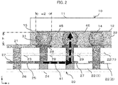
- FIG. 2 is a side transparent view taken along the line A-A of FIG. 1 of the electronic circuit according to the first embodiment of the present invention.
- description is specifically given of a configuration of an electronic circuit 1 according to the first embodiment.
- FIG. 1 three axes of xyz are illustrated, and, in FIG. 2 , two axes of xz are illustrated.
- a positional relationship and the like are expressed assuming a three-dimensional coordinate using those xyz axes.
- a positive direction side indicates an upper side.
- a surface positioned on the positive direction side is expressed as "upper surface”
- a surface opposing the upper surface is expressed as "lower surface”.
- Surfaces other than the upper surface and the lower surface are all "side surfaces”.
- the electronic circuit 1 is manufactured using flip chip mounting in which a first substrate 10 is stacked on a second substrate 20 along the z-axis direction and connected thereto.
- the first substrate 10 and the second substrate 20 are connected to each other through use of solder bumps 31.
- the first substrate 10 is, for example, a semiconductor chip. Throughout a lower surface of a layer 11 included in the first substrate 10, as illustrated in FIG. 1 and FIG. 2 , a dielectric body 15 is formed. On a lower surface of the dielectric body 15, an earth conductor 12, a coplanar line 13, and a plurality of pads 14 are formed.
- the earth conductor 12 is a planar pattern to be connected to the ground.
- the coplanar line 13 is provided for signal transmission.
- the coplanar line 13 is connected to one of the pads 14.
- the solder bump 31 being connected to the corresponding pad 14 is arranged.
- the earth conductor 12 corresponds to a ground conductor described in the scope of claims.
- the other second substrate 20 is a multilayer substrate in which a first layer 22(1) to a third layer 22(3) are laminated. On an upper surface of the first layer 22(1), a large number of lands 28 are formed, and a dielectric body 21 is formed in a part in which the lands 28 are absent. The solder bumps 31 are arranged on the lands 28, respectively. A space between the second substrate 20 and the first substrate 10 is filled with a dielectric body 32.
- each outline representing the solder bump 31, the pad 14, or the coplanar line 13 is non-transparent.
- parts of the third layer 22(3) positioned below a first transmission structure 45 and a second transmission structure 46 are illustrated as hatched rectangles. With this illustration, it is clearly shown that a via 26 included in the first transmission structure 45 and a via 26 included in the second transmission structure 46 are both formed so as to pass through only the first layer 22(1) and the second layer 22(2), and are absent in the third layer 22(3).
- the coplanar line 13 is not shown due to the presence of the earth conductor 12.
- the material of the layer 11 is, for example, silicon.
- the material of each of the first layer 22(1) to the third layer 22(3) is, for example, MEGTRON 6.
- the dielectric body 15 is, for example, polyimide.
- the dielectric body 32 is, for example, an adhesive called underfill.
- the dielectric body 21 is, for example, a resist. Each of the materials is not particularly limited.
- an earth conductor 23 is formed on an upper surface of the second layer 22(2), that is, between the second layer 22(2) and the first layer 22(1).
- the earth conductor 23 is a planar pattern connected to the ground.
- An upper surface of the third layer 22(3), that is, a space between the third layer 22(3) and the second layer 22(2) is used for a wiring line for signal transmission.
- a strip line 25 is illustrated as the wiring line therefor.
- an earth conductor 24 is formed on a lower surface of the third layer 22(3).
- the earth conductor 24 is a planar pattern connected to the ground.
- the vias 26 are columnar conductors for connection between layers.
- Each of the vias 26 is connected to a corresponding one of lands 27 formed on the upper surface of the third layer 22(3).
- the strip line 25 is connected to one of the lands 27, and the corresponding land 27 is connected to one of the vias 26.
- the upper side of the corresponding via 26 is connected to the land 28, and one of the solder bumps 31 is arranged on the corresponding land 28.
- the pad 14 is arranged on the corresponding solder bump 31.
- first transmission structure 45 those land 27, via 26, land 28, solder bump 31, and pad 14 are collectively expressed as "first transmission structure 45".
- the first transmission structure 45 has a space between the second layer 22(2) and the first layer 22(1), which corresponds to an inside of a hole 29.
- the hole 29 is structure for avoiding connection to the earth conductor 23 formed on the upper surface of the second layer 22(2). With this structure, the first transmission structure 45 is unconnected to the earth conductor 23.
- the first transmission structure 45 is connected to a different via 26 via a strip line 41 and a different land 27.
- the corresponding different land 27, the corresponding different via 26, the land 28 arranged on the corresponding different via 26, the solder bump 31 arranged on the corresponding land 28, and the pad 14 arranged on the corresponding solder bump 31 are collectively expressed as "second transmission structure 46".
- a combination including the land 27, the via 26, the land 28, the solder bump 31, and the pad 14 other than those of the first transmission structure 45 and the second transmission structure 46 is simply expressed as "structure”.
- the second transmission structure 46 also has a space between the second layer 22(2) and the first layer 22(1), which corresponds to the inside of the hole 29. With this structure, the second transmission structure 46 is also unconnected to the earth conductor 23.
- the pad 14 included in the first transmission structure 45 and the coplanar line 13 connected to the corresponding pad 14 are not connected to the earth conductor 12 formed in the first substrate 10. Meanwhile, the pad 14 included in the second transmission structure 46 and the pads 14 included in other structures are connected to the earth conductor 12. As illustrated in FIG. 1 and FIG. 2 , the other structures are connected to the earth conductor 23, that is, are connected to the ground. Therefore, the strip line 41 and the second transmission structure 46 function as a short-circuit stub.
- the two arrows of FIG. 2 represent paths of signals to be transmitted from the first transmission structure 45 to the earth conductor 12 via the strip line 41 and the second transmission structure 46.
- FIG. 3A is a top transparent view for illustrating the electronic circuit according to the first embodiment of the present invention.
- FIG. 3B is a bottom transparent view for illustrating the electronic circuit according to the first embodiment of the present invention.
- the strip line 41 arranged between the first transmission structure 45 and the second transmission structure 46 is configured to connect those structures to each other through the shortest path.
- the structures including those first transmission structure 45 and second transmission structure 46 are arranged in matrix on an xy plane.
- the second transmission structure 46 is positioned so that, on the xy plane, one structure is present between the second transmission structure 46 and the side surface of the first substrate 10, that is, a boundary of a range in which the first substrate 10 and the second substrate 20 overlap each other. Except for the first transmission structure 45, other structures around the second transmission structure 46 are all connected to the earth conductor 23.
- the second transmission structure 46 is arranged at a location having such a positional relationship for the purpose of preventing the strip line 41 from being arranged on a surface on an outer side of the second substrate 20 and achieving a large effect of suppressing unnecessary radiation from the other structures.
- An electrical length of the short-circuit stub including the strip line 41 and the second transmission structure 46 is an accumulated value of electrical lengths of the strip line 41 and the second transmission structure 46. It is important to set the electrical length of the short-circuit stub to be half a wavelength of a frequency that is assumed as an unnecessary wave.
- the first substrate 10 when the first substrate 10 operates as an amplifier and generates a second harmonic wave of an operation frequency as an unnecessary wave, in order to suppress the unnecessary wave of the second harmonic wave, it is important to set the electrical length of the short-circuit stub to be a length corresponding to the operation frequency.
- a pitch p between the structures of FIG. 3A is 500 ⁇ m
- a line width w1 of the strip line 25 is 85 ⁇ m.
- the dielectric constant is 11.9 in the layer 11 of the first substrate 10, and 3.62 in each of the first layer 22(1) to the third layer 22(3) of the second substrate 20.
- the solder bump 31 is sized so that a height h of FIG. 2 is about 250 ⁇ m and a width w2 is about 300 ⁇ m.
- FIG. 4 is a graph for showing results of electromagnetic field analysis of a reflection characteristic and a transmission characteristic based on presence or absence of the short-circuit stub, which is performed with respect to the electronic circuit having the structure of FIG. 1 .
- the horizontal axis represents frequency
- the vertical axis represents attenuation amount.
- the lines with a notation of "STUB PRESENT" all correspond to the analysis results in the first embodiment.
- the frequency passband and a suppression target band which is a band corresponding to a target of suppression, are indicated by broken lines.
- the reflection characteristic as shown in FIG. 4 , when the short-circuit stub is present, as compared to a case in which the short-circuit stub is absent, improvement is achieved by 10 dB or more in the frequency passband, and 15 dB or more in the suppression target band.
- the transmission characteristic as shown in FIG. 4 , when the short-circuit stub is present, as compared to the case in which the short-circuit stub is absent, slight improvement is achieved in the frequency passband, and improvement is achieved by 20 dB or more in the suppression target band. It has been confirmed based on those results that the short-circuit stub in the first embodiment allows great improvement in both of the reflection characteristic and the transmission characteristic.
- the via 26 serving as the columnar conductor is used as a part of the short-circuit stub.
- this via 26 is used, as compared to a case in which the strip line to be used as a short-circuit stub is formed on the surface on the outer side of the substrate, the length of the strip line 41 can be reduced.
- the upsizing of the electronic circuit 1 caused when the short-circuit stub is provided can be avoided, or can be greatly suppressed. Further, radiation of an unnecessary wave from the short-circuit stub is suppressed.
- Around the second transmission structure 46 structures connected to the ground are arranged. Therefore, radiation of an unnecessary wave is further suppressed.
- the structure arranged nearest to the first transmission structure 45 is the second transmission structure 46.
- a different structure is used as the second transmission structure.
- reference symbols used in the above-mentioned first embodiment are used as they are so that description is given in a way focusing only on parts different from the above-mentioned first embodiment.
- FIG. 5 is a top transparent view for illustrating an electronic circuit according to the second embodiment of the present invention.
- the structure to be connected to the first transmission structure 45 is a structure adjacent to the above-mentioned second transmission structure 46 on the positive direction side of the y axis.
- the second transmission structure 46 in the second embodiment has a space between the second layer 22(2) and the first layer 22(1), which corresponds to the inside of the hole 29, and is thus unconnected to the earth conductor 23.
- the structure arranged at the position of the second transmission structure 46 in the above-mentioned first embodiment is connected to the earth conductor 23.
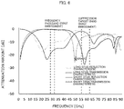
- FIG. 6 is a graph for showing results of electromagnetic field analysis of the reflection characteristic and the transmission characteristic based on a length of the short-circuit stub, which is performed with respect to the electronic circuit having the structure of FIG. 1 .
- the horizontal axis represents frequency
- the vertical axis represents attenuation amount.
- the lines with a notation of "LONG STUB” all correspond to the analysis results in the second embodiment.
- the lines with a notation of "SHORT STUB” all correspond to the analysis results in the above-mentioned first embodiment.
- FIG. 6 the analysis results of the above-mentioned first embodiment and the second embodiment are shown.
- the short-circuit stub is structured to include five types of conductors, specifically, the strip line 41 for connection on a layer, the via 26, the lands 27 and 28, the solder bump 31, and the pad 14.
- the types used in the short-circuit stub and the combination of those types are not limited to the above.
- the number of conductors used in each type is not limited to those in the above-mentioned first embodiment and the above-mentioned second embodiment.
- a plurality of strip lines 41 and a plurality of vias 26 may be used.
- the actual structure of the short-circuit stub can be modified in various ways.
- the strip line 25 is formed on the upper surface of the third layer 22(3).
- the strip line 25 is formed at this position, as compared to a case in which the strip line 25 is formed on the surface on the outer side of the second substrate 20, that is, on the upper surface of the first layer 22(1) or the lower surface of the third layer 22(3), radiation of an electromagnetic wave from the strip line 25 can be suppressed. Further, the following advantages can be obtained. Specifically, the via 26 can be easily used as the short-circuit stub, and troubles due to direct connection of the strip line 41 are less liable to occur.
Landscapes
- Engineering & Computer Science (AREA)
- Microelectronics & Electronic Packaging (AREA)
- Production Of Multi-Layered Print Wiring Board (AREA)
- Structure Of Printed Boards (AREA)
Claims (4)
- Elektronische Schaltung (1), bei der ein erstes Substrat (10) und ein zweites Substrat (20) gestapelt und miteinander verbunden sind, wobei die elektronische Schaltung umfasst:einen Übertragungspfad (14, 26 bis 28, 31), der eingerichtet ist, eine erste Verdrahtungsleitung (13) für ein Signal und eine zweite Verdrahtungsleitung (25) für ein Signal miteinander zu verbinden, wobei die erste Verdrahtungsleitung in dem ersten Substrat ausgebildet ist, und die zweite Verdrahtungsleitung in dem zweiten Substrat ausgebildet ist; undeine Kurzschluss-Stichleitung (41, 46), die eingerichtet ist, einen Erdungsleiter (12), der auf dem ersten Substrat vorgesehen ist, und den Übertragungspfad durch Verwendung von drei oder mehr Typen von Leitern miteinander zu verbinden;wobei das zweite Substrat ein Mehrschichtsubstrat ist, unddie Kurzschluss-Stichleitung als die drei oder mehr Typen von Leitern eine dritte Verdrahtungsleitung (41) zur Verbindung mit einer in dem zweiten Substrat enthaltenen Schicht (22(3)), einen säulenförmigen Leiter (26) zur Verbindung zwischen Schichten und einen Löthöcker (31) umfasst.
- Elektronische Schaltung nach Anspruch 1,wobei die zweite Verdrahtungsleitung auf einer Schicht (22(3)) ausgebildet ist, die zu einer Außenseite des zweiten Substrats hin nicht freigelegt ist, unddie dritte Verdrahtungsleitung mit der zweiten Verdrahtungsleitung verbunden ist.
- Elektronische Schaltung nach Anspruch 1 oder 2,
wobei ein oder mehrere andere geerdete säulenförmige Leiter (26) um den säulenförmigen Leiter angeordnet sind, der in der Kurzschluss-Stichleitung enthalten ist. - Elektronische Schaltung nach einem der Ansprüche 1 bis 3,
wobei in einem Bereich, in dem das erste Substrat und das zweite Substrat einander überlappen, der in der Kurzschluss-Stichleitung enthaltene säulenförmige Leiter an einer Position angeordnet ist, an der ein oder mehrere unterschiedliche säulenförmige Leiter (26) zwischen dem säulenförmigen Leiter und einer Grenze des Bereichs in einer orthogonalen Richtung orthogonal zu einer Richtung, in der das erste Substrat und das zweite Substrat gestapelt sind, vorhanden sind.
Applications Claiming Priority (1)
| Application Number | Priority Date | Filing Date | Title |
|---|---|---|---|
| PCT/JP2018/013634 WO2019187013A1 (ja) | 2018-03-30 | 2018-03-30 | 電子回路 |
Publications (3)
| Publication Number | Publication Date |
|---|---|
| EP3758136A1 EP3758136A1 (de) | 2020-12-30 |
| EP3758136A4 EP3758136A4 (de) | 2021-02-24 |
| EP3758136B1 true EP3758136B1 (de) | 2022-12-14 |
Family
ID=65270487
Family Applications (1)
| Application Number | Title | Priority Date | Filing Date |
|---|---|---|---|
| EP18912043.9A Active EP3758136B1 (de) | 2018-03-30 | 2018-03-30 | Elektronische schaltung |
Country Status (4)
| Country | Link |
|---|---|
| US (1) | US20200381376A1 (de) |
| EP (1) | EP3758136B1 (de) |
| JP (1) | JP6465451B1 (de) |
| WO (1) | WO2019187013A1 (de) |
Families Citing this family (2)
| Publication number | Priority date | Publication date | Assignee | Title |
|---|---|---|---|---|
| US11145609B2 (en) * | 2019-12-05 | 2021-10-12 | Nxp Usa, Inc. | Doherty amplifier with surface-mount packaged carrier and peaking amplifiers |
| US12548877B2 (en) * | 2022-10-05 | 2026-02-10 | Nxp B.V. | Printed circuit board (PCB) including a vertical launcher having a signal via for radiating signal energy through a PCB channel region |
Family Cites Families (7)
| Publication number | Priority date | Publication date | Assignee | Title |
|---|---|---|---|---|
| JP2004146810A (ja) * | 2002-09-30 | 2004-05-20 | Matsushita Electric Ind Co Ltd | プリント配線基板、ビルドアップ基板、プリント配線基板の製造方法、電子機器 |
| US7030712B2 (en) * | 2004-03-01 | 2006-04-18 | Belair Networks Inc. | Radio frequency (RF) circuit board topology |
| US8558637B2 (en) | 2010-05-12 | 2013-10-15 | Mediatek Inc. | Circuit device with signal line transition element |
| JP5861868B2 (ja) | 2011-11-04 | 2016-02-16 | ソニー株式会社 | 電子回路および電子回路の製造方法 |
| JP2017121032A (ja) * | 2015-06-30 | 2017-07-06 | 住友電気工業株式会社 | 高周波装置 |
| WO2018029846A1 (ja) * | 2016-08-12 | 2018-02-15 | 三菱電機株式会社 | 導波管ストリップ線路変換器及び給電回路 |
| GB2571214B (en) * | 2016-12-26 | 2021-07-14 | Mitsubishi Electric Corp | Terminal device |
-
2018
- 2018-03-30 JP JP2018546567A patent/JP6465451B1/ja active Active
- 2018-03-30 EP EP18912043.9A patent/EP3758136B1/de active Active
- 2018-03-30 WO PCT/JP2018/013634 patent/WO2019187013A1/ja not_active Ceased
-
2020
- 2020-08-19 US US16/997,572 patent/US20200381376A1/en not_active Abandoned
Also Published As
| Publication number | Publication date |
|---|---|
| US20200381376A1 (en) | 2020-12-03 |
| EP3758136A4 (de) | 2021-02-24 |
| EP3758136A1 (de) | 2020-12-30 |
| WO2019187013A1 (ja) | 2019-10-03 |
| JPWO2019187013A1 (ja) | 2020-04-30 |
| JP6465451B1 (ja) | 2019-02-06 |
Similar Documents
| Publication | Publication Date | Title |
|---|---|---|
| US11284506B2 (en) | High frequency module, board equipped with antenna, and high frequency circuit board | |
| US7405477B1 (en) | Ball grid array package-to-board interconnect co-design apparatus | |
| KR100891763B1 (ko) | 반도체 장치 | |
| US20150084208A1 (en) | Connection member, semiconductor device, and stacked structure | |
| US9713259B2 (en) | Communication module | |
| US10056669B2 (en) | Transmission line | |
| US10199335B2 (en) | Electronic device including coupling structure along with waveguide, and electronic equipment | |
| US9589908B1 (en) | Methods to improve BGA package isolation in radio frequency and millimeter wave products | |
| US9313877B2 (en) | Electronic device and noise suppression method | |
| CN101610636B (zh) | 电磁带隙结构及印刷电路板 | |
| US20200381376A1 (en) | Electronic circuit | |
| CN112397477B (zh) | 毫米波芯片封装系统 | |
| US7015574B2 (en) | Electronic device carrier adapted for transmitting high frequency signals | |
| JP3999177B2 (ja) | 高周波回路基板 | |
| TWI891985B (zh) | 微電子h框架裝置中之具有高隔離之射頻交越 | |
| US8385084B2 (en) | Shielding structures for signal paths in electronic devices | |
| EP2146557A1 (de) | Integrierte Mikrowellenschaltung | |
| WO2022230883A1 (ja) | 半導体パッケージ及び半導体電子装置 | |
| TWI237379B (en) | Chip package structure and circuit substrate thereof | |
| JP7151456B2 (ja) | インピーダンス補償回路 | |
| US9601818B2 (en) | Microwave circuit | |
| US12199053B2 (en) | Electronic device and semiconductor device | |
| US20250309153A1 (en) | Apparatus and Method for Mitigating Crosstalk in an Advanced Package | |
| KR102712113B1 (ko) | 칩-온-필름 패키지 | |
| WO2026088509A1 (ja) | プリント基板 |
Legal Events
| Date | Code | Title | Description |
|---|---|---|---|
| STAA | Information on the status of an ep patent application or granted ep patent |
Free format text: STATUS: THE INTERNATIONAL PUBLICATION HAS BEEN MADE |
|
| PUAI | Public reference made under article 153(3) epc to a published international application that has entered the european phase |
Free format text: ORIGINAL CODE: 0009012 |
|
| STAA | Information on the status of an ep patent application or granted ep patent |
Free format text: STATUS: REQUEST FOR EXAMINATION WAS MADE |
|
| 17P | Request for examination filed |
Effective date: 20200924 |
|
| AK | Designated contracting states |
Kind code of ref document: A1 Designated state(s): AL AT BE BG CH CY CZ DE DK EE ES FI FR GB GR HR HU IE IS IT LI LT LU LV MC MK MT NL NO PL PT RO RS SE SI SK SM TR |
|
| AX | Request for extension of the european patent |
Extension state: BA ME |
|
| A4 | Supplementary search report drawn up and despatched |
Effective date: 20210126 |
|
| RIC1 | Information provided on ipc code assigned before grant |
Ipc: H01P 5/02 20060101AFI20210120BHEP Ipc: H01L 23/66 20060101ALI20210120BHEP Ipc: H05K 1/02 20060101ALI20210120BHEP |
|
| DAV | Request for validation of the european patent (deleted) | ||
| DAX | Request for extension of the european patent (deleted) | ||
| GRAP | Despatch of communication of intention to grant a patent |
Free format text: ORIGINAL CODE: EPIDOSNIGR1 |
|
| RIC1 | Information provided on ipc code assigned before grant |
Ipc: H05K 1/11 20060101ALN20220531BHEP Ipc: H01L 23/00 20060101ALN20220531BHEP Ipc: H01L 23/498 20060101ALI20220531BHEP Ipc: H05K 1/02 20060101ALI20220531BHEP Ipc: H01L 23/66 20060101ALI20220531BHEP Ipc: H01P 5/02 20060101AFI20220531BHEP |
|
| STAA | Information on the status of an ep patent application or granted ep patent |
Free format text: STATUS: GRANT OF PATENT IS INTENDED |
|
| INTG | Intention to grant announced |
Effective date: 20220707 |
|
| GRAS | Grant fee paid |
Free format text: ORIGINAL CODE: EPIDOSNIGR3 |
|
| GRAA | (expected) grant |
Free format text: ORIGINAL CODE: 0009210 |
|
| STAA | Information on the status of an ep patent application or granted ep patent |
Free format text: STATUS: THE PATENT HAS BEEN GRANTED |
|
| AK | Designated contracting states |
Kind code of ref document: B1 Designated state(s): AL AT BE BG CH CY CZ DE DK EE ES FI FR GB GR HR HU IE IS IT LI LT LU LV MC MK MT NL NO PL PT RO RS SE SI SK SM TR |
|
| REG | Reference to a national code |
Ref country code: GB Ref legal event code: FG4D |
|
| REG | Reference to a national code |
Ref country code: CH Ref legal event code: EP |
|
| REG | Reference to a national code |
Ref country code: DE Ref legal event code: R096 Ref document number: 602018044375 Country of ref document: DE |
|
| REG | Reference to a national code |
Ref country code: IE Ref legal event code: FG4D |
|
| REG | Reference to a national code |
Ref country code: AT Ref legal event code: REF Ref document number: 1538222 Country of ref document: AT Kind code of ref document: T Effective date: 20230115 |
|
| REG | Reference to a national code |
Ref country code: LT Ref legal event code: MG9D |
|
| REG | Reference to a national code |
Ref country code: NL Ref legal event code: MP Effective date: 20221214 |
|
| PG25 | Lapsed in a contracting state [announced via postgrant information from national office to epo] |
Ref country code: SE Free format text: LAPSE BECAUSE OF FAILURE TO SUBMIT A TRANSLATION OF THE DESCRIPTION OR TO PAY THE FEE WITHIN THE PRESCRIBED TIME-LIMIT Effective date: 20221214 Ref country code: NO Free format text: LAPSE BECAUSE OF FAILURE TO SUBMIT A TRANSLATION OF THE DESCRIPTION OR TO PAY THE FEE WITHIN THE PRESCRIBED TIME-LIMIT Effective date: 20230314 Ref country code: LT Free format text: LAPSE BECAUSE OF FAILURE TO SUBMIT A TRANSLATION OF THE DESCRIPTION OR TO PAY THE FEE WITHIN THE PRESCRIBED TIME-LIMIT Effective date: 20221214 Ref country code: FI Free format text: LAPSE BECAUSE OF FAILURE TO SUBMIT A TRANSLATION OF THE DESCRIPTION OR TO PAY THE FEE WITHIN THE PRESCRIBED TIME-LIMIT Effective date: 20221214 |
|
| REG | Reference to a national code |
Ref country code: AT Ref legal event code: MK05 Ref document number: 1538222 Country of ref document: AT Kind code of ref document: T Effective date: 20221214 |
|
| PG25 | Lapsed in a contracting state [announced via postgrant information from national office to epo] |
Ref country code: RS Free format text: LAPSE BECAUSE OF FAILURE TO SUBMIT A TRANSLATION OF THE DESCRIPTION OR TO PAY THE FEE WITHIN THE PRESCRIBED TIME-LIMIT Effective date: 20221214 Ref country code: LV Free format text: LAPSE BECAUSE OF FAILURE TO SUBMIT A TRANSLATION OF THE DESCRIPTION OR TO PAY THE FEE WITHIN THE PRESCRIBED TIME-LIMIT Effective date: 20221214 Ref country code: HR Free format text: LAPSE BECAUSE OF FAILURE TO SUBMIT A TRANSLATION OF THE DESCRIPTION OR TO PAY THE FEE WITHIN THE PRESCRIBED TIME-LIMIT Effective date: 20221214 Ref country code: GR Free format text: LAPSE BECAUSE OF FAILURE TO SUBMIT A TRANSLATION OF THE DESCRIPTION OR TO PAY THE FEE WITHIN THE PRESCRIBED TIME-LIMIT Effective date: 20230315 |
|
| PG25 | Lapsed in a contracting state [announced via postgrant information from national office to epo] |
Ref country code: NL Free format text: LAPSE BECAUSE OF FAILURE TO SUBMIT A TRANSLATION OF THE DESCRIPTION OR TO PAY THE FEE WITHIN THE PRESCRIBED TIME-LIMIT Effective date: 20221214 |
|
| PG25 | Lapsed in a contracting state [announced via postgrant information from national office to epo] |
Ref country code: SM Free format text: LAPSE BECAUSE OF FAILURE TO SUBMIT A TRANSLATION OF THE DESCRIPTION OR TO PAY THE FEE WITHIN THE PRESCRIBED TIME-LIMIT Effective date: 20221214 Ref country code: RO Free format text: LAPSE BECAUSE OF FAILURE TO SUBMIT A TRANSLATION OF THE DESCRIPTION OR TO PAY THE FEE WITHIN THE PRESCRIBED TIME-LIMIT Effective date: 20221214 Ref country code: PT Free format text: LAPSE BECAUSE OF FAILURE TO SUBMIT A TRANSLATION OF THE DESCRIPTION OR TO PAY THE FEE WITHIN THE PRESCRIBED TIME-LIMIT Effective date: 20230414 Ref country code: ES Free format text: LAPSE BECAUSE OF FAILURE TO SUBMIT A TRANSLATION OF THE DESCRIPTION OR TO PAY THE FEE WITHIN THE PRESCRIBED TIME-LIMIT Effective date: 20221214 Ref country code: EE Free format text: LAPSE BECAUSE OF FAILURE TO SUBMIT A TRANSLATION OF THE DESCRIPTION OR TO PAY THE FEE WITHIN THE PRESCRIBED TIME-LIMIT Effective date: 20221214 Ref country code: CZ Free format text: LAPSE BECAUSE OF FAILURE TO SUBMIT A TRANSLATION OF THE DESCRIPTION OR TO PAY THE FEE WITHIN THE PRESCRIBED TIME-LIMIT Effective date: 20221214 Ref country code: AT Free format text: LAPSE BECAUSE OF FAILURE TO SUBMIT A TRANSLATION OF THE DESCRIPTION OR TO PAY THE FEE WITHIN THE PRESCRIBED TIME-LIMIT Effective date: 20221214 |
|
| P01 | Opt-out of the competence of the unified patent court (upc) registered |
Effective date: 20230711 |
|
| PG25 | Lapsed in a contracting state [announced via postgrant information from national office to epo] |
Ref country code: SK Free format text: LAPSE BECAUSE OF FAILURE TO SUBMIT A TRANSLATION OF THE DESCRIPTION OR TO PAY THE FEE WITHIN THE PRESCRIBED TIME-LIMIT Effective date: 20221214 Ref country code: PL Free format text: LAPSE BECAUSE OF FAILURE TO SUBMIT A TRANSLATION OF THE DESCRIPTION OR TO PAY THE FEE WITHIN THE PRESCRIBED TIME-LIMIT Effective date: 20221214 Ref country code: IS Free format text: LAPSE BECAUSE OF FAILURE TO SUBMIT A TRANSLATION OF THE DESCRIPTION OR TO PAY THE FEE WITHIN THE PRESCRIBED TIME-LIMIT Effective date: 20230414 Ref country code: AL Free format text: LAPSE BECAUSE OF FAILURE TO SUBMIT A TRANSLATION OF THE DESCRIPTION OR TO PAY THE FEE WITHIN THE PRESCRIBED TIME-LIMIT Effective date: 20221214 |
|
| REG | Reference to a national code |
Ref country code: DE Ref legal event code: R097 Ref document number: 602018044375 Country of ref document: DE |
|
| PLBE | No opposition filed within time limit |
Free format text: ORIGINAL CODE: 0009261 |
|
| STAA | Information on the status of an ep patent application or granted ep patent |
Free format text: STATUS: NO OPPOSITION FILED WITHIN TIME LIMIT |
|
| PG25 | Lapsed in a contracting state [announced via postgrant information from national office to epo] |
Ref country code: MC Free format text: LAPSE BECAUSE OF FAILURE TO SUBMIT A TRANSLATION OF THE DESCRIPTION OR TO PAY THE FEE WITHIN THE PRESCRIBED TIME-LIMIT Effective date: 20221214 Ref country code: DK Free format text: LAPSE BECAUSE OF FAILURE TO SUBMIT A TRANSLATION OF THE DESCRIPTION OR TO PAY THE FEE WITHIN THE PRESCRIBED TIME-LIMIT Effective date: 20221214 |
|
| REG | Reference to a national code |
Ref country code: CH Ref legal event code: PL |
|
| 26N | No opposition filed |
Effective date: 20230915 |
|
| GBPC | Gb: european patent ceased through non-payment of renewal fee |
Effective date: 20230330 |
|
| PG25 | Lapsed in a contracting state [announced via postgrant information from national office to epo] |
Ref country code: SI Free format text: LAPSE BECAUSE OF FAILURE TO SUBMIT A TRANSLATION OF THE DESCRIPTION OR TO PAY THE FEE WITHIN THE PRESCRIBED TIME-LIMIT Effective date: 20221214 |
|
| REG | Reference to a national code |
Ref country code: BE Ref legal event code: MM Effective date: 20230331 |
|
| PG25 | Lapsed in a contracting state [announced via postgrant information from national office to epo] |
Ref country code: LU Free format text: LAPSE BECAUSE OF NON-PAYMENT OF DUE FEES Effective date: 20230330 |
|
| REG | Reference to a national code |
Ref country code: IE Ref legal event code: MM4A |
|
| PG25 | Lapsed in a contracting state [announced via postgrant information from national office to epo] |
Ref country code: GB Free format text: LAPSE BECAUSE OF NON-PAYMENT OF DUE FEES Effective date: 20230330 |
|
| PG25 | Lapsed in a contracting state [announced via postgrant information from national office to epo] |
Ref country code: LI Free format text: LAPSE BECAUSE OF NON-PAYMENT OF DUE FEES Effective date: 20230331 Ref country code: IE Free format text: LAPSE BECAUSE OF NON-PAYMENT OF DUE FEES Effective date: 20230330 Ref country code: GB Free format text: LAPSE BECAUSE OF NON-PAYMENT OF DUE FEES Effective date: 20230330 Ref country code: CH Free format text: LAPSE BECAUSE OF NON-PAYMENT OF DUE FEES Effective date: 20230331 |
|
| PG25 | Lapsed in a contracting state [announced via postgrant information from national office to epo] |
Ref country code: BE Free format text: LAPSE BECAUSE OF NON-PAYMENT OF DUE FEES Effective date: 20230331 |
|
| PG25 | Lapsed in a contracting state [announced via postgrant information from national office to epo] |
Ref country code: IT Free format text: LAPSE BECAUSE OF FAILURE TO SUBMIT A TRANSLATION OF THE DESCRIPTION OR TO PAY THE FEE WITHIN THE PRESCRIBED TIME-LIMIT Effective date: 20221214 |
|
| PG25 | Lapsed in a contracting state [announced via postgrant information from national office to epo] |
Ref country code: BG Free format text: LAPSE BECAUSE OF FAILURE TO SUBMIT A TRANSLATION OF THE DESCRIPTION OR TO PAY THE FEE WITHIN THE PRESCRIBED TIME-LIMIT Effective date: 20221214 |
|
| PG25 | Lapsed in a contracting state [announced via postgrant information from national office to epo] |
Ref country code: BG Free format text: LAPSE BECAUSE OF FAILURE TO SUBMIT A TRANSLATION OF THE DESCRIPTION OR TO PAY THE FEE WITHIN THE PRESCRIBED TIME-LIMIT Effective date: 20221214 |
|
| PG25 | Lapsed in a contracting state [announced via postgrant information from national office to epo] |
Ref country code: CY Free format text: LAPSE BECAUSE OF FAILURE TO SUBMIT A TRANSLATION OF THE DESCRIPTION OR TO PAY THE FEE WITHIN THE PRESCRIBED TIME-LIMIT; INVALID AB INITIO Effective date: 20180330 |
|
| PG25 | Lapsed in a contracting state [announced via postgrant information from national office to epo] |
Ref country code: HU Free format text: LAPSE BECAUSE OF FAILURE TO SUBMIT A TRANSLATION OF THE DESCRIPTION OR TO PAY THE FEE WITHIN THE PRESCRIBED TIME-LIMIT; INVALID AB INITIO Effective date: 20180330 |
|
| PG25 | Lapsed in a contracting state [announced via postgrant information from national office to epo] |
Ref country code: TR Free format text: LAPSE BECAUSE OF FAILURE TO SUBMIT A TRANSLATION OF THE DESCRIPTION OR TO PAY THE FEE WITHIN THE PRESCRIBED TIME-LIMIT Effective date: 20221214 |
|
| PGFP | Annual fee paid to national office [announced via postgrant information from national office to epo] |
Ref country code: DE Payment date: 20260204 Year of fee payment: 9 |
|
| PGFP | Annual fee paid to national office [announced via postgrant information from national office to epo] |
Ref country code: FR Payment date: 20260209 Year of fee payment: 9 |