EP3757893B1 - Antennenstruktur, rfid-inlay, rfid-etikett und rfid-medium - Google Patents
Antennenstruktur, rfid-inlay, rfid-etikett und rfid-medium Download PDFInfo
- Publication number
- EP3757893B1 EP3757893B1 EP19757232.4A EP19757232A EP3757893B1 EP 3757893 B1 EP3757893 B1 EP 3757893B1 EP 19757232 A EP19757232 A EP 19757232A EP 3757893 B1 EP3757893 B1 EP 3757893B1
- Authority
- EP
- European Patent Office
- Prior art keywords
- long
- substrate
- sub
- rfid
- pair
- Prior art date
- Legal status (The legal status is an assumption and is not a legal conclusion. Google has not performed a legal analysis and makes no representation as to the accuracy of the status listed.)
- Active
Links
Images


Classifications
-
- H—ELECTRICITY
- H01—ELECTRIC ELEMENTS
- H01Q—ANTENNAS, i.e. RADIO AERIALS
- H01Q9/00—Electrically-short antennas having dimensions not more than twice the operating wavelength and consisting of conductive active radiating elements
- H01Q9/04—Resonant antennas
- H01Q9/06—Details
- H01Q9/065—Microstrip dipole antennas
-
- G—PHYSICS
- G06—COMPUTING OR CALCULATING; COUNTING
- G06K—GRAPHICAL DATA READING; PRESENTATION OF DATA; RECORD CARRIERS; HANDLING RECORD CARRIERS
- G06K19/00—Record carriers for use with machines and with at least a part designed to carry digital markings
- G06K19/06—Record carriers for use with machines and with at least a part designed to carry digital markings characterised by the kind of the digital marking, e.g. shape, nature, code
- G06K19/067—Record carriers with conductive marks, printed circuits or semiconductor circuit elements, e.g. credit or identity cards also with resonating or responding marks without active components
- G06K19/07—Record carriers with conductive marks, printed circuits or semiconductor circuit elements, e.g. credit or identity cards also with resonating or responding marks without active components with integrated circuit chips
- G06K19/077—Constructional details, e.g. mounting of circuits in the carrier
- G06K19/07749—Constructional details, e.g. mounting of circuits in the carrier the record carrier being capable of non-contact communication, e.g. constructional details of the antenna of a non-contact smart card
- G06K19/07773—Antenna details
- G06K19/07794—Antenna details the record carrier comprising a booster or auxiliary antenna in addition to the antenna connected directly to the integrated circuit
-
- B—PERFORMING OPERATIONS; TRANSPORTING
- B42—BOOKBINDING; ALBUMS; FILES; SPECIAL PRINTED MATTER
- B42D—BOOKS; BOOK COVERS; LOOSE LEAVES; PRINTED MATTER CHARACTERISED BY IDENTIFICATION OR SECURITY FEATURES; PRINTED MATTER OF SPECIAL FORMAT OR STYLE NOT OTHERWISE PROVIDED FOR; DEVICES FOR USE THEREWITH AND NOT OTHERWISE PROVIDED FOR; MOVABLE-STRIP WRITING OR READING APPARATUS
- B42D25/00—Information-bearing cards or sheet-like structures characterised by identification or security features; Manufacture thereof
- B42D25/30—Identification or security features, e.g. for preventing forgery
- B42D25/305—Associated digital information
-
- G—PHYSICS
- G06—COMPUTING OR CALCULATING; COUNTING
- G06K—GRAPHICAL DATA READING; PRESENTATION OF DATA; RECORD CARRIERS; HANDLING RECORD CARRIERS
- G06K19/00—Record carriers for use with machines and with at least a part designed to carry digital markings
- G06K19/06—Record carriers for use with machines and with at least a part designed to carry digital markings characterised by the kind of the digital marking, e.g. shape, nature, code
- G06K19/067—Record carriers with conductive marks, printed circuits or semiconductor circuit elements, e.g. credit or identity cards also with resonating or responding marks without active components
- G06K19/07—Record carriers with conductive marks, printed circuits or semiconductor circuit elements, e.g. credit or identity cards also with resonating or responding marks without active components with integrated circuit chips
- G06K19/0723—Record carriers with conductive marks, printed circuits or semiconductor circuit elements, e.g. credit or identity cards also with resonating or responding marks without active components with integrated circuit chips the record carrier comprising an arrangement for non-contact communication, e.g. wireless communication circuits on transponder cards, non-contact smart cards or RFIDs
-
- G—PHYSICS
- G06—COMPUTING OR CALCULATING; COUNTING
- G06K—GRAPHICAL DATA READING; PRESENTATION OF DATA; RECORD CARRIERS; HANDLING RECORD CARRIERS
- G06K19/00—Record carriers for use with machines and with at least a part designed to carry digital markings
- G06K19/06—Record carriers for use with machines and with at least a part designed to carry digital markings characterised by the kind of the digital marking, e.g. shape, nature, code
- G06K19/067—Record carriers with conductive marks, printed circuits or semiconductor circuit elements, e.g. credit or identity cards also with resonating or responding marks without active components
- G06K19/07—Record carriers with conductive marks, printed circuits or semiconductor circuit elements, e.g. credit or identity cards also with resonating or responding marks without active components with integrated circuit chips
- G06K19/077—Constructional details, e.g. mounting of circuits in the carrier
- G06K19/0772—Physical layout of the record carrier
- G06K19/07722—Physical layout of the record carrier the record carrier being multilayered, e.g. laminated sheets
-
- G—PHYSICS
- G06—COMPUTING OR CALCULATING; COUNTING
- G06K—GRAPHICAL DATA READING; PRESENTATION OF DATA; RECORD CARRIERS; HANDLING RECORD CARRIERS
- G06K19/00—Record carriers for use with machines and with at least a part designed to carry digital markings
- G06K19/06—Record carriers for use with machines and with at least a part designed to carry digital markings characterised by the kind of the digital marking, e.g. shape, nature, code
- G06K19/067—Record carriers with conductive marks, printed circuits or semiconductor circuit elements, e.g. credit or identity cards also with resonating or responding marks without active components
- G06K19/07—Record carriers with conductive marks, printed circuits or semiconductor circuit elements, e.g. credit or identity cards also with resonating or responding marks without active components with integrated circuit chips
- G06K19/077—Constructional details, e.g. mounting of circuits in the carrier
- G06K19/07749—Constructional details, e.g. mounting of circuits in the carrier the record carrier being capable of non-contact communication, e.g. constructional details of the antenna of a non-contact smart card
- G06K19/07758—Constructional details, e.g. mounting of circuits in the carrier the record carrier being capable of non-contact communication, e.g. constructional details of the antenna of a non-contact smart card arrangements for adhering the record carrier to further objects or living beings, functioning as an identification tag
- G06K19/0776—Constructional details, e.g. mounting of circuits in the carrier the record carrier being capable of non-contact communication, e.g. constructional details of the antenna of a non-contact smart card arrangements for adhering the record carrier to further objects or living beings, functioning as an identification tag the adhering arrangement being a layer of adhesive, so that the record carrier can function as a sticker
-
- G—PHYSICS
- G06—COMPUTING OR CALCULATING; COUNTING
- G06K—GRAPHICAL DATA READING; PRESENTATION OF DATA; RECORD CARRIERS; HANDLING RECORD CARRIERS
- G06K19/00—Record carriers for use with machines and with at least a part designed to carry digital markings
- G06K19/06—Record carriers for use with machines and with at least a part designed to carry digital markings characterised by the kind of the digital marking, e.g. shape, nature, code
- G06K19/067—Record carriers with conductive marks, printed circuits or semiconductor circuit elements, e.g. credit or identity cards also with resonating or responding marks without active components
- G06K19/07—Record carriers with conductive marks, printed circuits or semiconductor circuit elements, e.g. credit or identity cards also with resonating or responding marks without active components with integrated circuit chips
- G06K19/077—Constructional details, e.g. mounting of circuits in the carrier
- G06K19/07749—Constructional details, e.g. mounting of circuits in the carrier the record carrier being capable of non-contact communication, e.g. constructional details of the antenna of a non-contact smart card
- G06K19/07766—Constructional details, e.g. mounting of circuits in the carrier the record carrier being capable of non-contact communication, e.g. constructional details of the antenna of a non-contact smart card comprising at least a second communication arrangement in addition to a first non-contact communication arrangement
- G06K19/07767—Constructional details, e.g. mounting of circuits in the carrier the record carrier being capable of non-contact communication, e.g. constructional details of the antenna of a non-contact smart card comprising at least a second communication arrangement in addition to a first non-contact communication arrangement the first and second communication means being two different antennas types, e.g. dipole and coil type, or two antennas of the same kind but operating at different frequencies
-
- G—PHYSICS
- G06—COMPUTING OR CALCULATING; COUNTING
- G06K—GRAPHICAL DATA READING; PRESENTATION OF DATA; RECORD CARRIERS; HANDLING RECORD CARRIERS
- G06K19/00—Record carriers for use with machines and with at least a part designed to carry digital markings
- G06K19/06—Record carriers for use with machines and with at least a part designed to carry digital markings characterised by the kind of the digital marking, e.g. shape, nature, code
- G06K19/067—Record carriers with conductive marks, printed circuits or semiconductor circuit elements, e.g. credit or identity cards also with resonating or responding marks without active components
- G06K19/07—Record carriers with conductive marks, printed circuits or semiconductor circuit elements, e.g. credit or identity cards also with resonating or responding marks without active components with integrated circuit chips
- G06K19/077—Constructional details, e.g. mounting of circuits in the carrier
- G06K19/07749—Constructional details, e.g. mounting of circuits in the carrier the record carrier being capable of non-contact communication, e.g. constructional details of the antenna of a non-contact smart card
- G06K19/07773—Antenna details
- G06K19/07786—Antenna details the antenna being of the HF type, such as a dipole
-
- H—ELECTRICITY
- H01—ELECTRIC ELEMENTS
- H01Q—ANTENNAS, i.e. RADIO AERIALS
- H01Q1/00—Details of, or arrangements associated with, antennas
- H01Q1/12—Supports; Mounting means
- H01Q1/22—Supports; Mounting means by structural association with other equipment or articles
- H01Q1/2208—Supports; Mounting means by structural association with other equipment or articles associated with components used in interrogation type services, i.e. in systems for information exchange between an interrogator/reader and a tag/transponder, e.g. in Radio Frequency Identification [RFID] systems
- H01Q1/2225—Supports; Mounting means by structural association with other equipment or articles associated with components used in interrogation type services, i.e. in systems for information exchange between an interrogator/reader and a tag/transponder, e.g. in Radio Frequency Identification [RFID] systems used in active tags, i.e. provided with its own power source or in passive tags, i.e. deriving power from RF signal
-
- H—ELECTRICITY
- H01—ELECTRIC ELEMENTS
- H01Q—ANTENNAS, i.e. RADIO AERIALS
- H01Q1/00—Details of, or arrangements associated with, antennas
- H01Q1/36—Structural form of radiating elements, e.g. cone, spiral, umbrella; Particular materials used therewith
- H01Q1/38—Structural form of radiating elements, e.g. cone, spiral, umbrella; Particular materials used therewith formed by a conductive layer on an insulating support
-
- H—ELECTRICITY
- H01—ELECTRIC ELEMENTS
- H01Q—ANTENNAS, i.e. RADIO AERIALS
- H01Q7/00—Loop antennas with a substantially uniform current distribution around the loop and having a directional radiation pattern in a plane perpendicular to the plane of the loop
-
- H—ELECTRICITY
- H01—ELECTRIC ELEMENTS
- H01Q—ANTENNAS, i.e. RADIO AERIALS
- H01Q9/00—Electrically-short antennas having dimensions not more than twice the operating wavelength and consisting of conductive active radiating elements
- H01Q9/04—Resonant antennas
- H01Q9/16—Resonant antennas with feed intermediate between the extremities of the antenna, e.g. centre-fed dipole
- H01Q9/20—Two collinear substantially straight active elements; Substantially straight single active elements
- H01Q9/24—Shunt feed arrangements to single active elements, e.g. for delta matching
-
- H—ELECTRICITY
- H01—ELECTRIC ELEMENTS
- H01Q—ANTENNAS, i.e. RADIO AERIALS
- H01Q9/00—Electrically-short antennas having dimensions not more than twice the operating wavelength and consisting of conductive active radiating elements
- H01Q9/04—Resonant antennas
- H01Q9/16—Resonant antennas with feed intermediate between the extremities of the antenna, e.g. centre-fed dipole
- H01Q9/26—Resonant antennas with feed intermediate between the extremities of the antenna, e.g. centre-fed dipole with folded element or elements, the folded parts being spaced apart a small fraction of operating wavelength
-
- H—ELECTRICITY
- H01—ELECTRIC ELEMENTS
- H01Q—ANTENNAS, i.e. RADIO AERIALS
- H01Q9/00—Electrically-short antennas having dimensions not more than twice the operating wavelength and consisting of conductive active radiating elements
- H01Q9/04—Resonant antennas
- H01Q9/16—Resonant antennas with feed intermediate between the extremities of the antenna, e.g. centre-fed dipole
- H01Q9/28—Conical, cylindrical, cage, strip, gauze, or like elements having an extended radiating surface; Elements comprising two conical surfaces having collinear axes and adjacent apices and fed by two-conductor transmission lines
- H01Q9/285—Planar dipole
Definitions
- the present invention relates to an antenna pattern applied to a UHF frequency band RFID, an RFID inlay, an RFID label, and an RFID medium.
- tags that are attached to the products and labels that are adhered to the products, etc. are used. Information related to the products are printed on the tags and the labels so as to be visible.
- RFID Radio Frequency Identification
- an RFID medium On the tag, the label, an wrist band, and so forth (hereinafter, referred to as an RFID medium) are incorporated an antenna pattern and the IC chip with an RFID specification as described above, information related to a target for attachment, a target for affixation, or an wearer (hereinafter, collectively referred to as an adherend) is printed so as to be visible, and it is possible to store various information related to the adherend in the incorporated IC chip.
- an adherend information related to a target for attachment, a target for affixation, or an wearer
- Document US 2018/039878 A1 describes an RFID tag including an inlay (made of an IC chip and an antenna) and an auxiliary antenna laminated on the inlay in an insulated state.
- the auxiliary antenna is electrically coupled with the IC chip via capacitive coupling and functions as an antenna to improve/adjust the communication characteristics, in particular the range, of the inlay.
- a UHF frequency band RFID inlay having an IC chip, a loop portion connected with the IC chip, and a dipole antenna connected with the loop portion has been disclosed (see JP2010-237853A ).
- the RFID inlay described in JP2010-237853A has a directivity in which a good gain is obtained in the crossing direction with respect to the direction in which the dipole antenna extends, but the gain is poor in the direction in which the dipole antenna extends, and there is a problem in that, when a reader/writer is located in the latter direction, a transmission and reception of data becomes unstable.
- the RFID inlay is applied to, for example, an application in which entrance and exit of a holder of "ID-1" standard card specified in ISO/IEC 7810 is managed by mounting the RFID inlay on the card and an application in which a timing of finishing of a competitor is recorded by affixing the RFID inlay to a numbered bib, etc. of the competitor, there has been a problem in that transmission and reception of information cannot be performed correctly depending on an orientation of the RFID inlay or a positional relationship between the RFID inlay and an RFID reader.
- an object of the present invention is to increase a direction and range capable of performing transmission and reception by improving directivity of an antenna in a UHF frequency band RFID inlay.
- an antenna pattern for being used in a UHF frequency band RFID inlay, the antenna pattern comprising: a substrate; a dipole antenna formed on a front surface of the substrate with a metal foil; and a sub-element formed on a back surface of the substrate with the metal foil, wherein the dipole antenna is provided with: a loop portion having an IC chip connecting portion to which an IC chip is connected; a pair of meanders configured to respectively extend from the loop portion so as to be line symmetrical by being connected to the loop portion at end portions on one side; and capacitance hats respectively connected to the pair of meanders, and the sub-element has a pair of U-shapes, the sub-element being arranged such that opening sides of the U-shapes face with each other so as to be line symmetrical, the sub-element being formed such that a part thereof overlaps with the dipole antenna through the substrate.
- the RFID inlay 1 and an antenna pattern 10 according to a first embodiment of the present invention will be described.
- the RFID inlay 1 in this embodiment is a UHF frequency band RFID inlay.
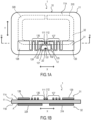
- FIG. 1A is an external view for explaining a front surface of the RFID inlay 1 according to the first embodiment
- FIG. 1B is a sectional view taken along a line B-B in FIG. 1A
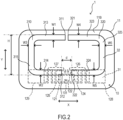
- FIG. 2 is an external view for explaining a back surface of the RFID inlay 1 according to the first embodiment.
- an IC chip 20 with an RFID (Radio Frequency Identification) specification is bonded to the antenna pattern 10 by a vulcanization bonding, etc. using an anisotropic conductive paste or a conductive film.
- the antenna pattern 10 is provided with a dipole antenna 31 that is formed on a front surface 11A of a substrate 11 with a metal foil and a sub-element 32 that is formed on a back surface 11B of the substrate 11 with the metal foil. As shown in FIG. 1B , the dipole antenna 31 and the sub-element 32 are laminated on the substrate 11 with an adhesive agent A.
- the sub-element 32 that is formed on the back surface 11B is illustrated with a dotted line.
- the dipole antenna 31 that is formed on the front surface 11A is illustrated with a dotted line.
- the direction in which the dipole antenna 31 extends is described as the X direction of the RFID inlay 1, and the direction perpendicular to the X direction is described as the Y direction of the RFID inlay 1.
- the dipole antenna 31 has a loop portion 12 that is formed on the front surface 11A of the substrate 11 with the metal foil and that has an IC chip connecting portion 101 to which the IC chip 20 is connected.
- the loop portion 12 is formed on the front surface 11A of the substrate 11 with the metal foil and has the IC chip connecting portion 101 to which the IC chip 20 is connected and a power feeding portion 102 to which meander end portions 111 and 112 of the dipole antenna 31 are connected.
- the loop portion 12 is formed to have a loop shape that is line symmetrical with respect to a line that passes through the IC chip connecting portion 101 and that is parallel to the Y direction.
- the loop portion 12 is formed to have a rectangular shape and has a pair of long-side portions 121 and 122 facing with each other.
- the loop portion 12 has a pair of short-side portions 124 and 125 that respectively connect end portions of the long-side portions 121 and 122 with each other.
- the IC chip connecting portion 101 is formed at the center portion of the long-side portion 121 on one side, and the power feeding portion 102 is formed towards the center portion side of the long-side portion 122 facing the long-side portion 121 on which the IC chip connecting portion 101 is formed.
- the dipole antenna 31 is formed in left-right symmetry with respect to the IC chip 20.
- the dipole antenna 31 has, on the front surface 11A, meanders 126 and 127 that are formed so as to extend in the opposite directions with each other with respect to the loop portion 12, and capacitance hats 128 and 129 that are connected to the meanders 126 and 127, respectively.
- connecting ends of the meanders 126 and 127 to the loop portion 12 correspond to the meander end portions 111 and 112, respectively.
- Number of folded portions, curvature radius of curved portions, lengths of the respective portions in the meanders 126 and 127 are set in consideration of an antenna efficiency.
- FIG. 2 the components formed on the front surface 11A are illustrated with dotted lines.
- the sub-element 32 formed on the back surface 11B has an element 310 on one side and an element 320 on the other side, and the element 310 and the element 320 each has U-shape and are formed such that their opening sides face each other so as to be in line symmetrical with respect to a line that passes through the IC chip 20 and that is parallel to the Y direction of the RFID inlay 1.
- the element 310 has parallel portions 313 and 314 that are formed in parallel with the X direction in which the dipole antenna 31 extends and a perpendicular portion 315 that joins end portions of the parallel portions 313 and 314.
- the element 320 has parallel portions 323 and 324 that are formed in parallel with the X direction in which the dipole antenna 31 extends and a perpendicular portion 325 that joins end portions of the parallel portions 323 and 324.
- the elements 310 and 320 having the U-shape are formed so as to be symmetrical with each other such that end portions (tip end portions) 311 and 321 on one side oppose to each other and end portions (base end portions) 312 and 322 on the other side oppose to each other.
- the base end portions 312 and 322 are formed so as to overlap with parts of the loop portion 12 through the substrate 11.
- the elements 310 and 320 formed in a U-shape have a gap formed by the base end portions 312 and 322 facing each other and a gap formed by the tip end portion s 311 and 321 facing each other.
- the IC chip connecting portion 101 of the loop portion 12 is positioned so as to overlap the gap formed by the base end portions 312 and 322 through the substrate 11.
- the widths W1 and W2 of the parallel portions 313 and 314 and the width W3 of the perpendicular portion 315 in the element 310, and the widths W4 and W5 of the parallel portions 323 and 324 and the width W6 of the perpendicular portion 325 in the element 320 are all formed so as to have the same width.
- the length H in the longitudinal direction Y including the widths of the respective elements and the widths W1 to W6 of the respective parts in the elements can be set in consideration of the antenna efficiency.
- the dipole antenna 31 and the sub-element 32 described above are formed on the substrate 11.
- a part of the sub-element 32 is formed so as to overlap with a part of the dipole antenna 31 through the substrate 11 and so as to overlap with a part of the long-side portion 122 on which the power feeding portion 102 is formed.
- the parallel portion 314 in the element 310 is formed so as to overlap with a part of the dipole antenna 31 on the upper side in the Y direction on the drawings over a region from the capacitance hat 129 to the meander 127.
- the parallel portion 324 in the element 320 is formed so as to overlap with a part of the dipole antenna 31 on the upper side in the Y direction on the drawings over a region from the capacitance hat 128 to the meander 126.
- a gap d between the base end portions 312 and 322 of the sub-element 32 facing with each other is formed at the position so as to sandwich the IC chip connecting portion 101 and the power feeding portion 102 in the loop portion 12 formed on the front surface 11A through the substrate 11.
- a material applicable as the substrate 11 includes papers such as fine quality paper, coated paper, and so forth; and a single film made of a resin such as polyvinyl chloride, polyethylene terephthalate, polypropylene, polyethylene, polyethylene naphthalate, and so forth, and a multilayer film formed by laminating a plurality of the resin films.
- papers such as fine quality paper, coated paper, and so forth
- a single film made of a resin such as polyvinyl chloride, polyethylene terephthalate, polypropylene, polyethylene, polyethylene naphthalate, and so forth, and a multilayer film formed by laminating a plurality of the resin films.
- the thickness of the substrate 11 is preferably from 25 pm to 300 pm, inclusive. In a case in which the papers are used as the substrate, the thickness can be from 50 pm to 260 pm, inclusive, in the above-described range, and it is generally preferable that the thickness be 80 pm. In addition, in a case in which the resin film is used as the substrate, the thickness can be from 25 pm to 200 pm, inclusive, in the above-described range. From the above, it is possible to make an appropriate selection depending on an application purpose.
- an electrically conductive metal used for forming the antenna pattern can be applied as a metal for forming the metal foil that is used for forming the loop portion 12 and the dipole antenna 31.
- One example thereof includes copper and aluminum.
- a thickness of the metal foil in view of an overall thickness of the RFID inlay 1, of an overall thickness of the RFID medium when the RFID medium is formed, and of the manufacturing cost, it is preferable that a thickness of the metal foil be from 3 pm to 25 pm, inclusive. More preferably, the metal foil is an aluminum foil having the thickness of 20 pm.
- the metal foil is adhered to the substrate 11 with the adhesive agent A.
- the dipole antenna 31 in the antenna pattern 10 is designed as a pattern adapted to a UHF frequency band (300 MHz to 3GHz, especially, 860 MHz to 960 MHz).
- the gain is poor in the longitudinal direction of the antenna (the X direction when associated with FIG. 1 ), and transmission and reception sensitivity in this direction is lowered.
- the RFID inlay 1 is provided with the sub-element 32.
- the sub-element 32 is formed so as to overlap with a part of the dipole antenna 31 through the substrate 11 and so as to overlap with a part of the long-side portion 122 in which the power feeding portion 102 is formed.
- the sub-element 32 has a function of compensating the gain of the dipole antenna 31 such that the RFID inlay 1 functions as an omnidirectional antenna.
- the elements 310 and 320 are formed such that all of their widths W1 to W6 are the same, and thereby, it is possible to keep an impedance in a transmission line in the elements 310 and 320 constant and to increase the antenna efficiency.
- An RFID inlay 2 and an antenna pattern 40 according to a second embodiment of the present invention will be described.
- a positional relationship between the dipole antenna 31 and a sub-element 33 is modified.
- the length H of the sub-element 33 in the Y direction is longer than that of the sub-element 32.
- the gap d between base end portions 332 and 342 is reduced.
- FIG. 3 is an external view for explaining a front surface of the RFID inlay 2 according to the second embodiment.
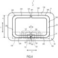
- FIG. 4 is an external view for explaining a back surface of the RFID inlay 2 according to the second embodiment. Configurations that have the same functions as the configurations shown in the first embodiment are assigned the same reference signs, and detailed descriptions thereof shall be omitted.
- the antenna pattern 40 has the substrate 11, the loop portion 12 that is formed on the front surface 11A of the substrate 11 with the metal foil, the dipole antenna 31 that is formed on the front surface 11A of the substrate 11 with the metal foil, and the sub-element 33 that is formed on the back surface 11B.
- the sub-element 33 that is formed on the back surface 11B has a left-right symmetric U-shapes on the back surface 11B and has an element 330 on one side and an element 340 on the other side.
- the element 330 has parallel portions 333 and 334 that are formed in parallel with the X direction in which the dipole antenna 31 extends and a perpendicular portion 335 that joins end portions of the parallel portions 333 and 334.
- the element 340 has parallel portions 343 and 344 that are formed in parallel with the X direction in which the dipole antenna 31 extends and a perpendicular portion 345 that joins end portions of the parallel portions 343 and 344.
- the elements 330 and 340 are formed so as to be symmetrical with each other such that the end portions (the tip end portions) 331 and 341 on one side oppose to each other and the end portions (the base end portions) 332 and 342 on the other side oppose to each other.
- the gap formed between the base end portions 332 and 342 is formed so as to be narrower than the gap formed between the base end portions 312 and 322 in the antenna pattern 10 that is shown as the first embodiment, and the IC chip 20 is formed so as to be positioned in the gap formed between the base end portions 332 and 342 through the substrate 11.
- all of the widths of the elements 330 and 340 are formed so as to have the same width.
- a part of the sub-element 33 is formed at the position where it overlaps with a part of the dipole antenna 31 through the substrate 11, and a part of the sub-element 33 is formed at the position where it intersects with the short-side portions 124 and 125 of the loop portion 12 through the substrate 11.
- a part of the sub-element 33 is formed at the position where it does not overlap with, through the substrate 11, the long-side portion 121 formed with the IC chip connecting portion 101 and the long-side portion 122 formed with the power feeding portion 102.
- a part of the sub-element 33 overlaps with a part of the dipole antenna 31 through the substrate 11, a part of the sub-element 33 intersects with the short-side portions 124 and 125, and a part of the sub-element 33 is formed so as not to overlap with the long-side portion 121 formed with the IC chip connecting portion 101and the long-side portion 122 formed with the power feeding portion 102.
- a sub-element 34 formed in the antenna pattern 50 is formed to have a shape in which base end portions 352 and 362 of the U-shape of elements 350 and 360 are each bent outwards of the U-shape.
- each of the elements 350 and 360 has a fishhook-like shape.
- FIG. 5 is an external view for explaining a front surface of the RFID inlay 3 according to the third embodiment.
- FIG. 6 is an external view for explaining a back surface of the RFID inlay 3 according to the third embodiment. Configurations that have the same functions as the configurations shown in the first embodiment are assigned the same reference signs, and detailed descriptions thereof shall be omitted.
- the antenna pattern 50 has the substrate 11, the loop portion 12 formed on the front surface 11A of the substrate 11 with the metal foil, the dipole antenna 31 formed on the front surface 11A of the substrate 11 with the metal foil, and the sub-element 34 formed on the back surface 11B.
- the sub-element 34 formed on the back surface 11B has a symmetrical shape on the back surface 11B and has the element 350 on one side and the element 360 on the other side.
- the element 350 has parallel portions 353 and 354 that are formed in parallel with the X direction in which the dipole antenna 31 extends and a perpendicular portion 355 that joins end portions of the parallel portions 353 and 354. Furthermore, in the element 350, an end portion of the parallel portion 354 forms a bent portion 356 by being bent outwards of the substrate 11.
- the element 360 has parallel portions 363 and 364 that are formed in parallel with the X direction in which the dipole antenna 31 extends and a perpendicular portion 365 that joins end portions of the parallel portions 363 and 364. Furthermore, in the element 360, an end portion of the parallel portion 364 forms a bent portion 366 by being bent outwards of the substrate 11.
- the elements 350 and 360 are formed so as to be symmetrical with each other such that the end portions (the tip end portions) 351 and 361 on one side oppose to each other and the end portions (the base end portions) 352 and 362 on the other side are both directed towards the outer side of the substrate 11.
- all of the widths of the elements 350 and 360 are formed so as to have the same width.
- a part of the sub-element 34 is formed at the position where it overlaps with a part of the dipole antenna 31 through the substrate 11 and at the position where it overlaps with a part of the long-side portion 122 formed with the power feeding portion 102.
- the parallel portion 354 in the element 350 is formed so as to overlap with a part of the dipole antenna 31 on the upper side in the Y direction on the drawings over a region from the capacitance hat 129 to the meander 127.
- the parallel portion 364 in the element 360 is formed so as to overlap with a part of the dipole antenna 31 on the upper side in the Y direction on the drawings over a region from the capacitance hat 128 to the meander 126.
- bent portions 356 and 366 that are each a part of the sub-element 34 are formed at the positions so as to cover the entire region of the short-side portions 124 and 125, respectively, through the substrate 11.
- the parallel portion 354 in the element 350 is formed so as to overlap with a part of the dipole antenna 31 on the upper side in the Y direction on the drawings through the substrate over a region from the capacitance hat 129 to the meander 127
- the parallel portion 364 in the element 360 are formed so as to overlap with a part of the dipole antenna 31 on the upper side in the Y direction on the drawings through the substrate 11 over a region from the capacitance hat 128 to the meander 126
- the bent portions 356 and 366 that are each a part of the sub-element 34 are formed at the positions so as to cover the entire regions of the short-side portions 124 and 125, respectively, through the substrate 11.
- the gain in the X direction of the RFID inlay 3 in FIGs. 5 and 6 is increased, and thereby, it is possible to increase the transmission and reception sensitivity in the X direction.
- the RFID label 5 is formed by temporarily adhering a separator on a first surface (or a second surface) of the RFID inlay 1, which has been described as the first embodiment, with the adhesive agent and by laminating an outer substrate on the second surface.
- FIG. 7 is a diagram for explaining a back surface of the RFID label 5 according to the embodiment of the present invention.
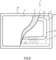
- FIG. 8 is a diagram for explaining a front surface of the RFID label 5 according to the embodiment of the present invention.
- the RFID label 5 has: a separator 60 that is temporarily adhered on the front surface 11A of the substrate 11 of the RFID inlay 1, which has been described as the first embodiment, with an adhesive agent B; and an outer substrate 70 that is laminated, with a bonding agent C, on the back surface 11B on the reverse side of the surface on which the separator 60 has been temporarily adhered.
- the outer substrate 70 serves as an information recording substrate that is a substrate having a surface suitable for printing.
- the outer substrate 70 may be a thermal paper.
- the adhesive agent B it is possible to use an adhesive agent that can be used with the separator and a bonding agent that can be used for lamination of the substrate.
- the bonding agent C it is possible to use those that can be used to laminate the substrates.
- the bonding agent C it may be possible to use emulsion bonding agents, solvent bonding agents, and hot melt bonding agents.
- the adhesive it is possible to apply acrylic bonding agents, urethane bonding agents, silicone bonding agents, rubber bonding agents, and so forth.
- the adhesive agent instead of the bonding agent C.
- the adhesive agent that can be used in this case includes the adhesive agent such as acrylic adhesives, urethane adhesives, silicone adhesives, rubber adhesives, and so forth.
- the RFID label 5 having such a configuration, information can be printed on the outer substrate 70 having a printing surface by using a label printer, and the RFID label 5 can be used by being adhered to a product, etc. by removing the separator 60.
- the integrated RFID inlay 1 has the sub-element 32 and antenna characteristics corresponding to those of the omnidirectional antenna can be achieved, even if the RFID label 5 according to this embodiment is used by being adhered to the product, etc., it is possible to perform the transmission and reception of data without being affected by positional relationship with a reader/writer.
- the outer substrate 70 may not necessarily be required for an application purpose in which the RFID label is adhered to a part that is not exposed to the outside.
- the RFID medium 6 is formed by laminating the outer substrates on both surfaces of the RFID inlay 1, which has been described as the first embodiment, with the adhesive agent.
- FIG. 9 is a diagram for explaining a front surface of the RFID medium 6 according to the embodiment of the present invention.
- FIG. 10 is a diagram for explaining a back surface of the RFID medium 6 according to the embodiment of the present invention.
- the RFID medium 6 has an outer substrate 80 that is laminated on the front surface 11A of the substrate 11 of the RFID inlay 1, which has been described as the first embodiment, with the bonding agent C and an outer substrate 90 that is laminated on the back surface 11B with the bonding agent C.
- the outer substrates 80 and 90 may be of the same type.
- the outer substrates 80 and 90 are each the substrate for recording information and may also be the substrate having the printing surface.
- An example of the RFID medium 6 having such a configuration includes an RFID tag.
- the RFID tag can be used by attaching it to apparel product, etc. by using a thread or a tag pin.
- the integrated RFID inlay 1 has the sub-element 32 and antenna characteristics corresponding to those of the omnidirectional antenna can be achieved, even if the RFID medium 6 according to this embodiment is used by being attached to the apparel product, etc., it is possible to perform the transmission and reception of data without being affected by positional relationship with a reader/writer.
- FIG. 12 is a schematic view for explaining the directivity test.
- a UHF frequency band RFID reader/writer R/W was arranged such that its antenna center is located on a position T on a circle having radius of 1.5 meter and having its center at a position P of the IC chip in the RFID tag as a test specimen S, and wave gain from the RFID tag was measured while moving the RFID reader/writer along the circle.
- the position of the reader/writer the above-described circle is expressed in terms of angle relative to the starting position where the angle is set as 0°, and relationships between the angle and wave gain are shown on a chart.
- the RFID tag of Example 1 is manufactured on the basis of the RFID medium 6 according to this embodiment described above.
- a basic configuration is as following: the dipole antenna 31 shown in FIG. 1 was formed with an aluminum foil having the thickness of 20 pm on the front surface of a substrate made of a PET film having the thickness of 50 pm, and on the back surface thereof, the sub-element 32 shown in FIG. 2 was formed with the aluminum foil having the thickness of 20 pm, thereby forming the antenna pattern 10.
- An IC (Monza R6 from Impinj, Inc.) was mounted on thus formed dipole antenna 31 to manufacture the RFID inlay 1 according to the first embodiment.
- the configuration on the dipole antenna 31 side had the same configuration as that of Product Number: ST7015 R6-RE01 from SATO HOLDINGS CORPORATION.
- the outer substrates 80 and 90 were laminated on both surfaces of the RFID inlay 1 obtained as described above by using the bonding agent C, and thereby, the RFID tag that was used as the test specimen was obtained.
- the RFID tag used as the test specimen was obtained similarly to Example 1 except that the sub-element 33 shown in FIG. 4 was used instead of the sub-element 32.
- the RFID tag used as the test specimen was obtained similarly to Example 1 except that the sub-element 34 shown in FIG. 6 was used instead of the sub-element 32.
- FIG. 11 is an external view for explaining the RFID tag as the comparative example used for the directivity test.
- the RFID tag R as the comparative example is formed by laminating the outer substrates 80 and 90 on Product Number: ST7015 R6-RE01 from SATO HOLDINGS CORPORATION.
- FIG. 13 is a diagram showing results for the directivity test for the measurement frequency.
- the gain is weak in the direction in which the dipole antenna extends (the X direction when associated with FIG. 1 ).
- the RFID tags of Examples 1, 2, and 3 that are respectively provided with the sub-element 32, 33, and 34, the gain in the X direction is increased.
- the sub-element on the RFID inlay it is possible to increase the gain in the extending direction of the dipole antenna 31 (the X direction) that is formed so as to be connected to the loop portion 12 and to extend in the X direction.
- the dipole antenna 31 is formed on the front surface 11A and the sub-element 32 is formed on the back surface 11B.
- the front surface 11A and the back surface 11B are named for the sake of ease of explaining, and a configuration in which, in FIGs. 1 and 2 , the sub-element 32 is formed on the front surface 11A and the dipole antenna 31 is formed on the back surface 11B has equivalent advantages.
- the U-shape includes a shape in which the portion corresponding to the bottom portion of the U-shape has an arc-shape, and a shape in which the portion corresponding to the bottom portion of the U-shape is a straight line and in which both ends of the straight line continues to parallel portions of the U-shape by being curved.
- the number or turns, turning shape, and so forth of the meanders 126 and 127 in the dipole antenna 31 shown in the embodiments can be modified appropriately, and the present invention is not limited to those illustrated.
- the RFID inlay 1 For the RFID label 5 shown in FIGs. 7 and 8 , and the RFID medium 6 shown in FIGs. 9 and 10 , although a description has been given of a case in which the RFID inlay 1 according to the first embodiment employing the antenna pattern 10 is applied, the RFID inlay 2 that employs the antenna pattern 40 and the RFID inlay 3 that employs the antenna pattern 50 may also be applied.
- the present invention is also applicable to an RFID card in which the RFID inlay is mounted on "ID-1" standard card specified in ISO/IEC 7810.
- the RFID inlay is employed to an application in which entrance and exit of a holder of the RFID card is managed and an application in which a timing of finishing of a competitor is recorded by affixing the RFID inlay to a numbered bib, etc. of the competitor, it becomes possible to perform the transmission and reception of data without being affected by the orientation of the RFID inlay and the positional relationship with the RFID reader.
Landscapes
- Engineering & Computer Science (AREA)
- Microelectronics & Electronic Packaging (AREA)
- Computer Hardware Design (AREA)
- Physics & Mathematics (AREA)
- General Physics & Mathematics (AREA)
- Theoretical Computer Science (AREA)
- Computer Networks & Wireless Communication (AREA)
- Details Of Aerials (AREA)
- Aerials With Secondary Devices (AREA)
Claims (10)
- Antennenstruktur (10) zum Einsatz in einem UHF-Frequenzband-RFID-Inlay, die umfasst:ein Substrat (11);eine Dipolantenne (31), die an einer Vorderseite (11A) des Substrats mit einer Metallfolie ausgebildet ist; undein Teilelement (32), das an einer Rückseite (11B) des Substrats mit der Metallfolie ausgebildet ist, wobeidie Dipol-Antenne (31) versehen ist mit:einem Schleifenabschnitt (12) mit einem IC-Chip-Verbindungsabschnitt (101), mit dem ein IC-Chip (20) verbunden ist;ein Paar von Mäanderstrukturen (126, 127), die so ausgeführt sind, dass sie sich jeweils so von dem Schleifenabschnitt (12) aus erstrecken, dass sie achsensymmetrisch sind, indem sie an Endabschnitten (111, 112) an einer Seite mit dem Schleifenabschnitt (12) verbunden sind; sowieKapazitätshüte (128, 129), die jeweils mit den paarigen Mäanderstrukturen (126, 127) verbunden sind, wobeidas Teilelement (32) so ausgebildet ist, dass sich ein Teil desselben mit der Dipolantenne (31) über das Substrat (11) überlappt,dadurch gekennzeichnet, dassdas Teilelement (32) ein Paar von U-Formen aufweist, wobei das Teilelement so angeordnet ist, dass Öffnungsseiten der U-Formen einander so zugewandt sind, dass sie achsensymmetrisch sind.
- Antennenstruktur (10) nach Anspruch 1, wobei jeweilige Basis-Endabschnitte (312, 322) in den paarigen U-Formen des Teilelementes (32) so ausgebildet sind, dass sie sich mit einem Teil des Schleifenabschnitts (12) über das Substrat (11) überlappen.
- Antennenstruktur (10) nach Anspruch 1, wobei der IC-Chip-Verbindungsabschnitt (101) des Schleifenabschnitts (12) über das Substrat (11) angeordnet ist in:einem Spalt zwischen jeweiligen Basis-Endabschnitten (312, 322) der paarigen U-Formen des Teilelementes (32), wobei der Spalt durch die einander zugewandten Basis-Endabschnitte (312, 322) gebildet wird; odereinem Spalt zwischen jeweiligen Spitzen-Endabschnitten (311, 321) der paarigen U-Formen des Teilelementes (32), wobei der Spalt durch die einander zugewandten Spitzen-Endabschnitte (311, 321) gebildet wird.
- Antennenstruktur (10) nach Anspruch 1, wobeider Schleifenabschnitt (12) eine rechteckige Form mit einander zugewandten paarigen Abschnitten (121, 122) der langen Seiten sowie paarigen Abschnitten (124, 125) der kurzen Seiten hat, die so ausgeführt sind, dass sie Endteile der Abschnitte (121, 122) der langen Seiten miteinander verbinden,der IC-Chip-Verbindungsabschnitt (101) an einem der Abschnitte (121) der langen Seiten ausgebildet ist und die Mäanderstruktur (126, 127) mit dem Abschnitt (122) der langen Seite verbunden ist, der dem Abschnitt (121) der langen Seite zugewandt ist, an dem der IC-Chip-Verbindungsabschnitt (101) ausgebildet ist, undein Teil des Teilelementes (32) sich mit einem Teil der Dipolantenne (31) über das Substrat (11) überlappt und sich mit einem Teil des Abschnitts (122) der langen Seite überlappt, mit dem die Mäanderstruktur (126, 127) verbunden ist.
- Antennenstruktur (10) nach Anspruch 1, wobeider Schleifenabschnitt (12) eine rechteckige Form mit einander zugewandten paarigen Abschnitten (121, 122) der langen Seiten sowie paarigen Abschnitten (124, 125) der kurzen Seiten hat, die so ausgeführt sind, dass sie Endabschnitte der Abschnitte (121, 122) der langen Seiten verbinden,der IC-Chip-Verbindungsabschnitt (101) an einem der Abschnitte (121) der langen Seiten ausgebildet ist, unddie Mäanderstruktur (126, 127) mit dem Abschnitt (122) der langen Seite verbunden ist, der dem Abschnitt (121) der langen Seite zugewandt ist, an dem der IC-Chip-Verbindungsabschnitt (101) ausgebildet ist, undein Teil des Teilelementes (32) sich mit einem Teil der Dipolantenne (31) über das Substrat (11) überlappt und sich mit dem Abschnitt (124, 125) der kurzen Seite schneidet, sich jedoch nicht mit dem Abschnitt (122) der langen Seite, an dem der IC-Chip-Verbindungsabschnitt (101) ausgebildet ist und dem Abschnitt (122) der langen Seite überlappt, mit dem die Mäanderstruktur (126, 127) verbunden ist.
- Antennenstruktur (10) nach Anspruch 1, wobeider Schleifenabschnitt (12) eine rechteckige Form mit einander zugewandten paarigen Abschnitten (121, 122) der langen Seiten sowie paarigen Abschnitten (124, 125) der kurzen Seiten hat, die so ausgeführt sind, dass sie Endabschnitte der Abschnitte (121, 122) der langen Seiten verbinden,der IC-Chip-Verbindungsabschnitt (101) an einem der Abschnitte (121) der langen Seiten ausgebildet ist, unddie Mäanderstruktur (126, 127) mit dem Abschnitt (122) der langen Seite verbunden ist, der dem Abschnitt (121) der langen Seite zugewandt ist, an dem der IC-Chip-Verbindungsabschnitt (101) ausgebildet ist, undein Teil des Teilelementes (32) sich mit einem Teil der Dipolantenne (31) über das Substrat (11) überlappt, einen gesamten Bereich des Abschnitts (124, 125) der kurzen Seite abdeckt, und sich einem Teil des Abschnitts (122) der langen Seite, an dem der IC-Chip-Verbindungsabschnitt (101) ausgebildet ist, sowie einem Teil des Abschnitts (122) der langen Seite überlappt, mit dem die Mäanderstruktur (126, 127) verbunden ist.
- UHF-Frequenzband-RFID-Inlay (1), das umfasst:
die Antennenstruktur (10) nach einem der Ansprüche 1 bis 6 sowie den IC-Chip (20), der mit dem IC-Chip-Verbindungsabschnitt (101) in der Antennenstruktur (10) verbunden ist. - RFID-Etikett (5), das das UHF-Frequenzband-RFID-Inlay nach Anspruch 7 umfasst, wobei ein Separator (60) temporär mit einem Haftmittel (C) an eine der Flächen des UHF-Frequenzband-RFID-Inlays angeheftet wird.
- RFID-Etikett (5), das das UHF-Frequenzband-RFID-Inlay nach Anspruch 7 umfasst, wobei ein Separator (60) temporär mit einem Haftmittel (C) an eine der Flächen des UHF-Frequenzband-RFID-Inlays (1) angeheftet wird und ein Informationsaufzeichnungs-Substrat (70) auf eine Fläche an einer Rückseite der Fläche laminiert wird, an der der Separator (60) temporär angeheftet ist.
- RFID-Medium (6), das das UHF-Frequenzband-RFID-Inlay nach Anspruch 7 umfasst, wobei beide Flächen des UHF-Frequenzband-RFID-Inlays (1) mit einem Klebstoff von einer Vielzahl äußerer Substrate (80, 90) eingeschlossen werden.
Applications Claiming Priority (2)
| Application Number | Priority Date | Filing Date | Title |
|---|---|---|---|
| JP2018029074A JP6941069B2 (ja) | 2018-02-21 | 2018-02-21 | アンテナパターン、rfidインレイ、rfidラベル及びrfid媒体 |
| PCT/JP2019/003509 WO2019163473A1 (ja) | 2018-02-21 | 2019-01-31 | アンテナパターン、rfidインレイ、rfidラベル及びrfid媒体 |
Publications (3)
| Publication Number | Publication Date |
|---|---|
| EP3757893A1 EP3757893A1 (de) | 2020-12-30 |
| EP3757893A4 EP3757893A4 (de) | 2021-05-05 |
| EP3757893B1 true EP3757893B1 (de) | 2023-08-23 |
Family
ID=67688289
Family Applications (1)
| Application Number | Title | Priority Date | Filing Date |
|---|---|---|---|
| EP19757232.4A Active EP3757893B1 (de) | 2018-02-21 | 2019-01-31 | Antennenstruktur, rfid-inlay, rfid-etikett und rfid-medium |
Country Status (5)
| Country | Link |
|---|---|
| US (1) | US11227205B2 (de) |
| EP (1) | EP3757893B1 (de) |
| JP (1) | JP6941069B2 (de) |
| CN (1) | CN111566672B (de) |
| WO (1) | WO2019163473A1 (de) |
Families Citing this family (17)
| Publication number | Priority date | Publication date | Assignee | Title |
|---|---|---|---|---|
| JP6941068B2 (ja) * | 2018-02-21 | 2021-09-29 | サトーホールディングス株式会社 | アンテナパターンの製造方法、rfidインレイの製造方法、rfidラベルの製造方法及びrfid媒体の製造方法 |
| HUE071018T2 (hu) | 2019-08-08 | 2025-07-28 | Sumitomo Bakelite Co | Kapszulázó gyantaösszetétel és elektronikai komponens |
| CN113285206B (zh) * | 2021-05-26 | 2022-06-07 | 湖南工程学院 | 一种小型化全向uhf-rfid标签天线及其制备方法 |
| USD1001785S1 (en) * | 2022-01-27 | 2023-10-17 | Avery Dennison Retail Information Services Llc | Antenna |
| USD1003876S1 (en) * | 2022-01-27 | 2023-11-07 | Avery Dennison Retail Information Services Llc | Antenna |
| JP2023115681A (ja) * | 2022-02-08 | 2023-08-21 | サトーホールディングス株式会社 | アンテナパターン、rfidインレイ |
| USD1007485S1 (en) * | 2022-02-16 | 2023-12-12 | Avery Dennison Retail Information Services Llc | Antenna |
| USD1003283S1 (en) * | 2022-02-16 | 2023-10-31 | Avery Dennison Retail Information Services Llc | Antenna |
| USD1002598S1 (en) * | 2022-02-17 | 2023-10-24 | Avery Dennison Retail Information Services Llc | Antenna |
| USD1004578S1 (en) * | 2022-03-24 | 2023-11-14 | Avery Dennison Retail Information Services Llc | Antenna |
| US20250343345A1 (en) * | 2022-06-03 | 2025-11-06 | Checkpoint Systems, Inc. | Rfid antenna for rejecting unwanted rf signals |
| USD1051885S1 (en) * | 2023-06-01 | 2024-11-19 | Ccl Label, Inc. | RFID inlay |
| USD1051107S1 (en) * | 2023-06-01 | 2024-11-12 | Ccl Label, Inc. | RFID inlay |
| USD1052563S1 (en) * | 2023-06-01 | 2024-11-26 | Ccl Label, Inc. | RFID inlay |
| USD1046835S1 (en) * | 2023-07-28 | 2024-10-15 | Avery Dennison Retail Information Security LLC | Antenna |
| USD1060319S1 (en) * | 2023-07-28 | 2025-02-04 | Avery Dennison Retail Information Services Llc | Antenna |
| US20250132498A1 (en) * | 2023-10-20 | 2025-04-24 | Toppan Holdings Inc. | Rfid tag and antenna pattern |
Citations (1)
| Publication number | Priority date | Publication date | Assignee | Title |
|---|---|---|---|---|
| EP2866298B1 (de) * | 2012-06-26 | 2020-05-06 | Toyo Seikan Group Holdings, Ltd. | Hf-etikett |
Family Cites Families (8)
| Publication number | Priority date | Publication date | Assignee | Title |
|---|---|---|---|---|
| JP5208830B2 (ja) | 2009-03-30 | 2013-06-12 | 株式会社サトー知識財産研究所 | Rfidラベルロールおよびrfidラベルロールの製造方法 |
| JP2011182392A (ja) * | 2010-02-08 | 2011-09-15 | Sinfonia Technology Co Ltd | ダイポール型icタグ用アンテナ、アンテナロール及びicタグの使用方法 |
| US9722006B2 (en) | 2012-02-21 | 2017-08-01 | Joled Inc. | Organic light-emitting device and method for producing same |
| JP5953978B2 (ja) * | 2012-06-26 | 2016-07-20 | 東洋製罐株式会社 | Rfタグ |
| EP2866172B1 (de) | 2012-06-26 | 2017-05-17 | Toyo Seikan Group Holdings, Ltd. | Rf-etikett |
| JP5910883B2 (ja) * | 2012-09-11 | 2016-04-27 | 株式会社 ワイテックス | 無線タグ用複合アンテナ |
| KR20190137184A (ko) * | 2015-04-21 | 2019-12-10 | 도요세이칸 그룹 홀딩스 가부시키가이샤 | Rf 태그 |
| JP6853237B2 (ja) * | 2016-03-18 | 2021-03-31 | サトーホールディングス株式会社 | アンテナパターンの製造方法、rfidインレットの製造方法、rfidラベルの製造方法及びrfid媒体の製造方法 |
-
2018
- 2018-02-21 JP JP2018029074A patent/JP6941069B2/ja active Active
-
2019
- 2019-01-31 EP EP19757232.4A patent/EP3757893B1/de active Active
- 2019-01-31 CN CN201980007823.8A patent/CN111566672B/zh active Active
- 2019-01-31 US US16/961,023 patent/US11227205B2/en active Active
- 2019-01-31 WO PCT/JP2019/003509 patent/WO2019163473A1/ja not_active Ceased
Patent Citations (1)
| Publication number | Priority date | Publication date | Assignee | Title |
|---|---|---|---|---|
| EP2866298B1 (de) * | 2012-06-26 | 2020-05-06 | Toyo Seikan Group Holdings, Ltd. | Hf-etikett |
Also Published As
| Publication number | Publication date |
|---|---|
| US11227205B2 (en) | 2022-01-18 |
| WO2019163473A1 (ja) | 2019-08-29 |
| CN111566672A (zh) | 2020-08-21 |
| CN111566672B (zh) | 2023-08-15 |
| EP3757893A1 (de) | 2020-12-30 |
| JP6941069B2 (ja) | 2021-09-29 |
| JP2019146043A (ja) | 2019-08-29 |
| US20200373674A1 (en) | 2020-11-26 |
| EP3757893A4 (de) | 2021-05-05 |
Similar Documents
| Publication | Publication Date | Title |
|---|---|---|
| EP3757893B1 (de) | Antennenstruktur, rfid-inlay, rfid-etikett und rfid-medium | |
| KR100679502B1 (ko) | Rfid 태그, rfid 태그용 안테나, rfid 태그용안테나 시트, 및 rfid 태그 제조 방법 | |
| US7434739B2 (en) | Antenna circuit, IC inlet, IC tag, and IC card, as well as manufacturing method of IC tag and manufacturing method of IC card | |
| US7292148B2 (en) | Method of variable position strap mounting for RFID transponder | |
| TWI382595B (zh) | Antenna construction of RFID transponder and its manufacturing method | |
| US12014235B2 (en) | Wireless communication device | |
| EP1898488A1 (de) | Hochfrequenz-identifikationsetikett | |
| US12141638B2 (en) | RFID label and method of using RFID label | |
| JP7131227B2 (ja) | Rfタグラベル | |
| CN209963236U (zh) | 无线通信器件 | |
| CN113348469A (zh) | 无线通信器件及其制造方法 | |
| WO2023153049A1 (ja) | アンテナパターン、rfidインレイ | |
| JP2020071807A (ja) | Rfタグラベルおよびrfタグラベル付き物品 | |
| WO2006134658A1 (ja) | Rfidタグアンテナ及びrfidタグ | |
| US7427919B2 (en) | RFID tag set, RFID tag and RFID tag component | |
| JP7014027B2 (ja) | Rfタグラベルおよびrfタグ構造体 | |
| JP7176313B2 (ja) | Rfタグラベル | |
| JP7183651B2 (ja) | Rfタグラベル | |
| JP2002358497A (ja) | 非接触式データキャリア装置用補助アンテナ部材、および該補助用アンテナ部材を配設した物品 | |
| WO2019031534A1 (ja) | Rfタグ用アンテナおよびrfタグ | |
| JP2025101163A (ja) | Rfidタグ及び下げ札 | |
| JP6614533B2 (ja) | 非接触型データ受送信体およびその使用方法 | |
| KR20080012998A (ko) | 무선 주파수 식별 태그 | |
| JP2021140671A (ja) | Rfidインレイ |
Legal Events
| Date | Code | Title | Description |
|---|---|---|---|
| STAA | Information on the status of an ep patent application or granted ep patent |
Free format text: STATUS: THE INTERNATIONAL PUBLICATION HAS BEEN MADE |
|
| PUAI | Public reference made under article 153(3) epc to a published international application that has entered the european phase |
Free format text: ORIGINAL CODE: 0009012 |
|
| STAA | Information on the status of an ep patent application or granted ep patent |
Free format text: STATUS: REQUEST FOR EXAMINATION WAS MADE |
|
| 17P | Request for examination filed |
Effective date: 20200710 |
|
| AK | Designated contracting states |
Kind code of ref document: A1 Designated state(s): AL AT BE BG CH CY CZ DE DK EE ES FI FR GB GR HR HU IE IS IT LI LT LU LV MC MK MT NL NO PL PT RO RS SE SI SK SM TR |
|
| AX | Request for extension of the european patent |
Extension state: BA ME |
|
| A4 | Supplementary search report drawn up and despatched |
Effective date: 20210406 |
|
| RIC1 | Information provided on ipc code assigned before grant |
Ipc: G06K 19/077 20060101AFI20210329BHEP Ipc: B42D 25/305 20140101ALI20210329BHEP Ipc: H01Q 9/26 20060101ALI20210329BHEP Ipc: H01Q 19/02 20060101ALI20210329BHEP |
|
| DAV | Request for validation of the european patent (deleted) | ||
| DAX | Request for extension of the european patent (deleted) | ||
| GRAP | Despatch of communication of intention to grant a patent |
Free format text: ORIGINAL CODE: EPIDOSNIGR1 |
|
| STAA | Information on the status of an ep patent application or granted ep patent |
Free format text: STATUS: GRANT OF PATENT IS INTENDED |
|
| INTG | Intention to grant announced |
Effective date: 20230314 |
|
| GRAS | Grant fee paid |
Free format text: ORIGINAL CODE: EPIDOSNIGR3 |
|
| GRAA | (expected) grant |
Free format text: ORIGINAL CODE: 0009210 |
|
| STAA | Information on the status of an ep patent application or granted ep patent |
Free format text: STATUS: THE PATENT HAS BEEN GRANTED |
|
| AK | Designated contracting states |
Kind code of ref document: B1 Designated state(s): AL AT BE BG CH CY CZ DE DK EE ES FI FR GB GR HR HU IE IS IT LI LT LU LV MC MK MT NL NO PL PT RO RS SE SI SK SM TR |
|
| REG | Reference to a national code |
Ref country code: GB Ref legal event code: FG4D |
|
| REG | Reference to a national code |
Ref country code: CH Ref legal event code: EP |
|
| REG | Reference to a national code |
Ref country code: IE Ref legal event code: FG4D |
|
| REG | Reference to a national code |
Ref country code: DE Ref legal event code: R096 Ref document number: 602019035639 Country of ref document: DE |
|
| REG | Reference to a national code |
Ref country code: LT Ref legal event code: MG9D |
|
| REG | Reference to a national code |
Ref country code: NL Ref legal event code: MP Effective date: 20230823 |
|
| REG | Reference to a national code |
Ref country code: AT Ref legal event code: MK05 Ref document number: 1603451 Country of ref document: AT Kind code of ref document: T Effective date: 20230823 |
|
| PG25 | Lapsed in a contracting state [announced via postgrant information from national office to epo] |
Ref country code: GR Free format text: LAPSE BECAUSE OF FAILURE TO SUBMIT A TRANSLATION OF THE DESCRIPTION OR TO PAY THE FEE WITHIN THE PRESCRIBED TIME-LIMIT Effective date: 20231124 |
|
| PG25 | Lapsed in a contracting state [announced via postgrant information from national office to epo] |
Ref country code: IS Free format text: LAPSE BECAUSE OF FAILURE TO SUBMIT A TRANSLATION OF THE DESCRIPTION OR TO PAY THE FEE WITHIN THE PRESCRIBED TIME-LIMIT Effective date: 20231223 |
|
| PG25 | Lapsed in a contracting state [announced via postgrant information from national office to epo] |
Ref country code: SE Free format text: LAPSE BECAUSE OF FAILURE TO SUBMIT A TRANSLATION OF THE DESCRIPTION OR TO PAY THE FEE WITHIN THE PRESCRIBED TIME-LIMIT Effective date: 20230823 Ref country code: RS Free format text: LAPSE BECAUSE OF FAILURE TO SUBMIT A TRANSLATION OF THE DESCRIPTION OR TO PAY THE FEE WITHIN THE PRESCRIBED TIME-LIMIT Effective date: 20230823 Ref country code: PT Free format text: LAPSE BECAUSE OF FAILURE TO SUBMIT A TRANSLATION OF THE DESCRIPTION OR TO PAY THE FEE WITHIN THE PRESCRIBED TIME-LIMIT Effective date: 20231226 Ref country code: NO Free format text: LAPSE BECAUSE OF FAILURE TO SUBMIT A TRANSLATION OF THE DESCRIPTION OR TO PAY THE FEE WITHIN THE PRESCRIBED TIME-LIMIT Effective date: 20231123 Ref country code: NL Free format text: LAPSE BECAUSE OF FAILURE TO SUBMIT A TRANSLATION OF THE DESCRIPTION OR TO PAY THE FEE WITHIN THE PRESCRIBED TIME-LIMIT Effective date: 20230823 Ref country code: LV Free format text: LAPSE BECAUSE OF FAILURE TO SUBMIT A TRANSLATION OF THE DESCRIPTION OR TO PAY THE FEE WITHIN THE PRESCRIBED TIME-LIMIT Effective date: 20230823 Ref country code: LT Free format text: LAPSE BECAUSE OF FAILURE TO SUBMIT A TRANSLATION OF THE DESCRIPTION OR TO PAY THE FEE WITHIN THE PRESCRIBED TIME-LIMIT Effective date: 20230823 Ref country code: IS Free format text: LAPSE BECAUSE OF FAILURE TO SUBMIT A TRANSLATION OF THE DESCRIPTION OR TO PAY THE FEE WITHIN THE PRESCRIBED TIME-LIMIT Effective date: 20231223 Ref country code: HR Free format text: LAPSE BECAUSE OF FAILURE TO SUBMIT A TRANSLATION OF THE DESCRIPTION OR TO PAY THE FEE WITHIN THE PRESCRIBED TIME-LIMIT Effective date: 20230823 Ref country code: GR Free format text: LAPSE BECAUSE OF FAILURE TO SUBMIT A TRANSLATION OF THE DESCRIPTION OR TO PAY THE FEE WITHIN THE PRESCRIBED TIME-LIMIT Effective date: 20231124 Ref country code: FI Free format text: LAPSE BECAUSE OF FAILURE TO SUBMIT A TRANSLATION OF THE DESCRIPTION OR TO PAY THE FEE WITHIN THE PRESCRIBED TIME-LIMIT Effective date: 20230823 Ref country code: AT Free format text: LAPSE BECAUSE OF FAILURE TO SUBMIT A TRANSLATION OF THE DESCRIPTION OR TO PAY THE FEE WITHIN THE PRESCRIBED TIME-LIMIT Effective date: 20230823 |
|
| PG25 | Lapsed in a contracting state [announced via postgrant information from national office to epo] |
Ref country code: PL Free format text: LAPSE BECAUSE OF FAILURE TO SUBMIT A TRANSLATION OF THE DESCRIPTION OR TO PAY THE FEE WITHIN THE PRESCRIBED TIME-LIMIT Effective date: 20230823 |
|
| PG25 | Lapsed in a contracting state [announced via postgrant information from national office to epo] |
Ref country code: ES Free format text: LAPSE BECAUSE OF FAILURE TO SUBMIT A TRANSLATION OF THE DESCRIPTION OR TO PAY THE FEE WITHIN THE PRESCRIBED TIME-LIMIT Effective date: 20230823 |
|
| PG25 | Lapsed in a contracting state [announced via postgrant information from national office to epo] |
Ref country code: SM Free format text: LAPSE BECAUSE OF FAILURE TO SUBMIT A TRANSLATION OF THE DESCRIPTION OR TO PAY THE FEE WITHIN THE PRESCRIBED TIME-LIMIT Effective date: 20230823 Ref country code: RO Free format text: LAPSE BECAUSE OF FAILURE TO SUBMIT A TRANSLATION OF THE DESCRIPTION OR TO PAY THE FEE WITHIN THE PRESCRIBED TIME-LIMIT Effective date: 20230823 Ref country code: ES Free format text: LAPSE BECAUSE OF FAILURE TO SUBMIT A TRANSLATION OF THE DESCRIPTION OR TO PAY THE FEE WITHIN THE PRESCRIBED TIME-LIMIT Effective date: 20230823 Ref country code: EE Free format text: LAPSE BECAUSE OF FAILURE TO SUBMIT A TRANSLATION OF THE DESCRIPTION OR TO PAY THE FEE WITHIN THE PRESCRIBED TIME-LIMIT Effective date: 20230823 Ref country code: DK Free format text: LAPSE BECAUSE OF FAILURE TO SUBMIT A TRANSLATION OF THE DESCRIPTION OR TO PAY THE FEE WITHIN THE PRESCRIBED TIME-LIMIT Effective date: 20230823 Ref country code: CZ Free format text: LAPSE BECAUSE OF FAILURE TO SUBMIT A TRANSLATION OF THE DESCRIPTION OR TO PAY THE FEE WITHIN THE PRESCRIBED TIME-LIMIT Effective date: 20230823 Ref country code: SK Free format text: LAPSE BECAUSE OF FAILURE TO SUBMIT A TRANSLATION OF THE DESCRIPTION OR TO PAY THE FEE WITHIN THE PRESCRIBED TIME-LIMIT Effective date: 20230823 |
|
| REG | Reference to a national code |
Ref country code: DE Ref legal event code: R097 Ref document number: 602019035639 Country of ref document: DE |
|
| PG25 | Lapsed in a contracting state [announced via postgrant information from national office to epo] |
Ref country code: IT Free format text: LAPSE BECAUSE OF FAILURE TO SUBMIT A TRANSLATION OF THE DESCRIPTION OR TO PAY THE FEE WITHIN THE PRESCRIBED TIME-LIMIT Effective date: 20230823 |
|
| PLBE | No opposition filed within time limit |
Free format text: ORIGINAL CODE: 0009261 |
|
| STAA | Information on the status of an ep patent application or granted ep patent |
Free format text: STATUS: NO OPPOSITION FILED WITHIN TIME LIMIT |
|
| 26N | No opposition filed |
Effective date: 20240524 |
|
| PG25 | Lapsed in a contracting state [announced via postgrant information from national office to epo] |
Ref country code: SI Free format text: LAPSE BECAUSE OF FAILURE TO SUBMIT A TRANSLATION OF THE DESCRIPTION OR TO PAY THE FEE WITHIN THE PRESCRIBED TIME-LIMIT Effective date: 20230823 |
|
| PG25 | Lapsed in a contracting state [announced via postgrant information from national office to epo] |
Ref country code: MC Free format text: LAPSE BECAUSE OF FAILURE TO SUBMIT A TRANSLATION OF THE DESCRIPTION OR TO PAY THE FEE WITHIN THE PRESCRIBED TIME-LIMIT Effective date: 20230823 |
|
| PG25 | Lapsed in a contracting state [announced via postgrant information from national office to epo] |
Ref country code: MC Free format text: LAPSE BECAUSE OF FAILURE TO SUBMIT A TRANSLATION OF THE DESCRIPTION OR TO PAY THE FEE WITHIN THE PRESCRIBED TIME-LIMIT Effective date: 20230823 |
|
| REG | Reference to a national code |
Ref country code: CH Ref legal event code: PL |
|
| PG25 | Lapsed in a contracting state [announced via postgrant information from national office to epo] |
Ref country code: LU Free format text: LAPSE BECAUSE OF NON-PAYMENT OF DUE FEES Effective date: 20240131 |
|
| PG25 | Lapsed in a contracting state [announced via postgrant information from national office to epo] |
Ref country code: LU Free format text: LAPSE BECAUSE OF NON-PAYMENT OF DUE FEES Effective date: 20240131 |
|
| PG25 | Lapsed in a contracting state [announced via postgrant information from national office to epo] |
Ref country code: BE Free format text: LAPSE BECAUSE OF NON-PAYMENT OF DUE FEES Effective date: 20240131 |
|
| PG25 | Lapsed in a contracting state [announced via postgrant information from national office to epo] |
Ref country code: CH Free format text: LAPSE BECAUSE OF NON-PAYMENT OF DUE FEES Effective date: 20240131 |
|
| PG25 | Lapsed in a contracting state [announced via postgrant information from national office to epo] |
Ref country code: CH Free format text: LAPSE BECAUSE OF NON-PAYMENT OF DUE FEES Effective date: 20240131 Ref country code: BE Free format text: LAPSE BECAUSE OF NON-PAYMENT OF DUE FEES Effective date: 20240131 |
|
| REG | Reference to a national code |
Ref country code: BE Ref legal event code: MM Effective date: 20240131 |
|
| PG25 | Lapsed in a contracting state [announced via postgrant information from national office to epo] |
Ref country code: BG Free format text: LAPSE BECAUSE OF FAILURE TO SUBMIT A TRANSLATION OF THE DESCRIPTION OR TO PAY THE FEE WITHIN THE PRESCRIBED TIME-LIMIT Effective date: 20230823 |
|
| PG25 | Lapsed in a contracting state [announced via postgrant information from national office to epo] |
Ref country code: BG Free format text: LAPSE BECAUSE OF FAILURE TO SUBMIT A TRANSLATION OF THE DESCRIPTION OR TO PAY THE FEE WITHIN THE PRESCRIBED TIME-LIMIT Effective date: 20230823 |
|
| PG25 | Lapsed in a contracting state [announced via postgrant information from national office to epo] |
Ref country code: IE Free format text: LAPSE BECAUSE OF NON-PAYMENT OF DUE FEES Effective date: 20240131 |
|
| PG25 | Lapsed in a contracting state [announced via postgrant information from national office to epo] |
Ref country code: IE Free format text: LAPSE BECAUSE OF NON-PAYMENT OF DUE FEES Effective date: 20240131 |
|
| PGFP | Annual fee paid to national office [announced via postgrant information from national office to epo] |
Ref country code: DE Payment date: 20250121 Year of fee payment: 7 |
|
| PGFP | Annual fee paid to national office [announced via postgrant information from national office to epo] |
Ref country code: FR Payment date: 20250127 Year of fee payment: 7 |
|
| PGFP | Annual fee paid to national office [announced via postgrant information from national office to epo] |
Ref country code: GB Payment date: 20250128 Year of fee payment: 7 |
|
| PG25 | Lapsed in a contracting state [announced via postgrant information from national office to epo] |
Ref country code: CY Free format text: LAPSE BECAUSE OF FAILURE TO SUBMIT A TRANSLATION OF THE DESCRIPTION OR TO PAY THE FEE WITHIN THE PRESCRIBED TIME-LIMIT; INVALID AB INITIO Effective date: 20190131 |
|
| PG25 | Lapsed in a contracting state [announced via postgrant information from national office to epo] |
Ref country code: HU Free format text: LAPSE BECAUSE OF FAILURE TO SUBMIT A TRANSLATION OF THE DESCRIPTION OR TO PAY THE FEE WITHIN THE PRESCRIBED TIME-LIMIT; INVALID AB INITIO Effective date: 20190131 |
|
| PG25 | Lapsed in a contracting state [announced via postgrant information from national office to epo] |
Ref country code: TR Free format text: LAPSE BECAUSE OF FAILURE TO SUBMIT A TRANSLATION OF THE DESCRIPTION OR TO PAY THE FEE WITHIN THE PRESCRIBED TIME-LIMIT Effective date: 20230823 |