EP3754701A1 - Kupfer/titan/aluminium-verbindung, isolierende leiterplatte, isolierende leiterplatte mit kühlkörper, leistungsmodul, led-modul und thermoelektrisches modul - Google Patents
Kupfer/titan/aluminium-verbindung, isolierende leiterplatte, isolierende leiterplatte mit kühlkörper, leistungsmodul, led-modul und thermoelektrisches modul Download PDFInfo
- Publication number
- EP3754701A1 EP3754701A1 EP18906230.0A EP18906230A EP3754701A1 EP 3754701 A1 EP3754701 A1 EP 3754701A1 EP 18906230 A EP18906230 A EP 18906230A EP 3754701 A1 EP3754701 A1 EP 3754701A1
- Authority
- EP
- European Patent Office
- Prior art keywords
- copper
- layer
- bonded
- titanium
- aluminum
- Prior art date
- Legal status (The legal status is an assumption and is not a legal conclusion. Google has not performed a legal analysis and makes no representation as to the accuracy of the status listed.)
- Granted
Links
Images




Classifications
-
- H—ELECTRICITY
- H10—SEMICONDUCTOR DEVICES; ELECTRIC SOLID-STATE DEVICES NOT OTHERWISE PROVIDED FOR
- H10W—GENERIC PACKAGES, INTERCONNECTIONS, CONNECTORS OR OTHER CONSTRUCTIONAL DETAILS OF DEVICES COVERED BY CLASS H10
- H10W70/00—Package substrates; Interposers; Redistribution layers [RDL]
- H10W70/60—Insulating or insulated package substrates; Interposers; Redistribution layers
- H10W70/67—Insulating or insulated package substrates; Interposers; Redistribution layers characterised by their insulating layers or insulating parts
- H10W70/68—Shapes or dispositions thereof
- H10W70/6875—Shapes or dispositions thereof being on a metallic substrate, e.g. insulated metal substrates [IMS]
-
- H—ELECTRICITY
- H10—SEMICONDUCTOR DEVICES; ELECTRIC SOLID-STATE DEVICES NOT OTHERWISE PROVIDED FOR
- H10W—GENERIC PACKAGES, INTERCONNECTIONS, CONNECTORS OR OTHER CONSTRUCTIONAL DETAILS OF DEVICES COVERED BY CLASS H10
- H10W40/00—Arrangements for thermal protection or thermal control
- H10W40/20—Arrangements for cooling
- H10W40/25—Arrangements for cooling characterised by their materials
- H10W40/255—Arrangements for cooling characterised by their materials having a laminate or multilayered structure, e.g. direct bond copper [DBC] ceramic substrates
-
- B—PERFORMING OPERATIONS; TRANSPORTING
- B23—MACHINE TOOLS; METAL-WORKING NOT OTHERWISE PROVIDED FOR
- B23K—SOLDERING OR UNSOLDERING; WELDING; CLADDING OR PLATING BY SOLDERING OR WELDING; CUTTING BY APPLYING HEAT LOCALLY, e.g. FLAME CUTTING; WORKING BY LASER BEAM
- B23K20/00—Non-electric welding by applying impact or other pressure, with or without the application of heat, e.g. cladding or plating
-
- B—PERFORMING OPERATIONS; TRANSPORTING
- B32—LAYERED PRODUCTS
- B32B—LAYERED PRODUCTS, i.e. PRODUCTS BUILT-UP OF STRATA OF FLAT OR NON-FLAT, e.g. CELLULAR OR HONEYCOMB, FORM
- B32B15/00—Layered products comprising a layer of metal
- B32B15/04—Layered products comprising a layer of metal comprising metal as the main or only constituent of a layer, which is next to another layer of the same or of a different material
-
- B—PERFORMING OPERATIONS; TRANSPORTING
- B32—LAYERED PRODUCTS
- B32B—LAYERED PRODUCTS, i.e. PRODUCTS BUILT-UP OF STRATA OF FLAT OR NON-FLAT, e.g. CELLULAR OR HONEYCOMB, FORM
- B32B15/00—Layered products comprising a layer of metal
- B32B15/20—Layered products comprising a layer of metal comprising aluminium or copper
-
- H—ELECTRICITY
- H10—SEMICONDUCTOR DEVICES; ELECTRIC SOLID-STATE DEVICES NOT OTHERWISE PROVIDED FOR
- H10H—INORGANIC LIGHT-EMITTING SEMICONDUCTOR DEVICES HAVING POTENTIAL BARRIERS
- H10H20/00—Individual inorganic light-emitting semiconductor devices having potential barriers, e.g. light-emitting diodes [LED]
- H10H20/80—Constructional details
- H10H20/85—Packages
- H10H20/858—Means for heat extraction or cooling
-
- H—ELECTRICITY
- H10—SEMICONDUCTOR DEVICES; ELECTRIC SOLID-STATE DEVICES NOT OTHERWISE PROVIDED FOR
- H10H—INORGANIC LIGHT-EMITTING SEMICONDUCTOR DEVICES HAVING POTENTIAL BARRIERS
- H10H20/00—Individual inorganic light-emitting semiconductor devices having potential barriers, e.g. light-emitting diodes [LED]
- H10H20/80—Constructional details
- H10H20/85—Packages
- H10H20/858—Means for heat extraction or cooling
- H10H20/8581—Means for heat extraction or cooling characterised by their material
-
- H—ELECTRICITY
- H10—SEMICONDUCTOR DEVICES; ELECTRIC SOLID-STATE DEVICES NOT OTHERWISE PROVIDED FOR
- H10H—INORGANIC LIGHT-EMITTING SEMICONDUCTOR DEVICES HAVING POTENTIAL BARRIERS
- H10H20/00—Individual inorganic light-emitting semiconductor devices having potential barriers, e.g. light-emitting diodes [LED]
- H10H20/80—Constructional details
- H10H20/85—Packages
- H10H20/858—Means for heat extraction or cooling
- H10H20/8585—Means for heat extraction or cooling being an interconnection
-
- H—ELECTRICITY
- H10—SEMICONDUCTOR DEVICES; ELECTRIC SOLID-STATE DEVICES NOT OTHERWISE PROVIDED FOR
- H10N—ELECTRIC SOLID-STATE DEVICES NOT OTHERWISE PROVIDED FOR
- H10N10/00—Thermoelectric devices comprising a junction of dissimilar materials, i.e. devices exhibiting Seebeck or Peltier effects
- H10N10/10—Thermoelectric devices comprising a junction of dissimilar materials, i.e. devices exhibiting Seebeck or Peltier effects operating with only the Peltier or Seebeck effects
- H10N10/17—Thermoelectric devices comprising a junction of dissimilar materials, i.e. devices exhibiting Seebeck or Peltier effects operating with only the Peltier or Seebeck effects characterised by the structure or configuration of the cell or thermocouple forming the device
-
- H—ELECTRICITY
- H10—SEMICONDUCTOR DEVICES; ELECTRIC SOLID-STATE DEVICES NOT OTHERWISE PROVIDED FOR
- H10N—ELECTRIC SOLID-STATE DEVICES NOT OTHERWISE PROVIDED FOR
- H10N10/00—Thermoelectric devices comprising a junction of dissimilar materials, i.e. devices exhibiting Seebeck or Peltier effects
- H10N10/80—Constructional details
-
- H—ELECTRICITY
- H10—SEMICONDUCTOR DEVICES; ELECTRIC SOLID-STATE DEVICES NOT OTHERWISE PROVIDED FOR
- H10W—GENERIC PACKAGES, INTERCONNECTIONS, CONNECTORS OR OTHER CONSTRUCTIONAL DETAILS OF DEVICES COVERED BY CLASS H10
- H10W40/00—Arrangements for thermal protection or thermal control
- H10W40/20—Arrangements for cooling
- H10W40/22—Arrangements for cooling characterised by their shape, e.g. having conical or cylindrical projections
-
- H—ELECTRICITY
- H10—SEMICONDUCTOR DEVICES; ELECTRIC SOLID-STATE DEVICES NOT OTHERWISE PROVIDED FOR
- H10W—GENERIC PACKAGES, INTERCONNECTIONS, CONNECTORS OR OTHER CONSTRUCTIONAL DETAILS OF DEVICES COVERED BY CLASS H10
- H10W40/00—Arrangements for thermal protection or thermal control
- H10W40/20—Arrangements for cooling
- H10W40/25—Arrangements for cooling characterised by their materials
- H10W40/258—Metallic materials
-
- H—ELECTRICITY
- H10—SEMICONDUCTOR DEVICES; ELECTRIC SOLID-STATE DEVICES NOT OTHERWISE PROVIDED FOR
- H10W—GENERIC PACKAGES, INTERCONNECTIONS, CONNECTORS OR OTHER CONSTRUCTIONAL DETAILS OF DEVICES COVERED BY CLASS H10
- H10W70/00—Package substrates; Interposers; Redistribution layers [RDL]
- H10W70/01—Manufacture or treatment
- H10W70/02—Manufacture or treatment of conductive package substrates serving as an interconnection, e.g. of metal plates
-
- H—ELECTRICITY
- H10—SEMICONDUCTOR DEVICES; ELECTRIC SOLID-STATE DEVICES NOT OTHERWISE PROVIDED FOR
- H10W—GENERIC PACKAGES, INTERCONNECTIONS, CONNECTORS OR OTHER CONSTRUCTIONAL DETAILS OF DEVICES COVERED BY CLASS H10
- H10W70/00—Package substrates; Interposers; Redistribution layers [RDL]
- H10W70/60—Insulating or insulated package substrates; Interposers; Redistribution layers
- H10W70/62—Insulating or insulated package substrates; Interposers; Redistribution layers characterised by their interconnections
- H10W70/66—Conductive materials thereof
-
- H—ELECTRICITY
- H10—SEMICONDUCTOR DEVICES; ELECTRIC SOLID-STATE DEVICES NOT OTHERWISE PROVIDED FOR
- H10W—GENERIC PACKAGES, INTERCONNECTIONS, CONNECTORS OR OTHER CONSTRUCTIONAL DETAILS OF DEVICES COVERED BY CLASS H10
- H10W70/00—Package substrates; Interposers; Redistribution layers [RDL]
- H10W70/60—Insulating or insulated package substrates; Interposers; Redistribution layers
- H10W70/67—Insulating or insulated package substrates; Interposers; Redistribution layers characterised by their insulating layers or insulating parts
- H10W70/69—Insulating materials thereof
- H10W70/692—Ceramics or glasses
-
- H—ELECTRICITY
- H10—SEMICONDUCTOR DEVICES; ELECTRIC SOLID-STATE DEVICES NOT OTHERWISE PROVIDED FOR
- H10W—GENERIC PACKAGES, INTERCONNECTIONS, CONNECTORS OR OTHER CONSTRUCTIONAL DETAILS OF DEVICES COVERED BY CLASS H10
- H10W72/00—Interconnections or connectors in packages
-
- H—ELECTRICITY
- H10—SEMICONDUCTOR DEVICES; ELECTRIC SOLID-STATE DEVICES NOT OTHERWISE PROVIDED FOR
- H10P—GENERIC PROCESSES OR APPARATUS FOR THE MANUFACTURE OR TREATMENT OF DEVICES COVERED BY CLASS H10
- H10P95/00—Generic processes or apparatus for manufacture or treatments not covered by the other groups of this subclass
-
- H—ELECTRICITY
- H10—SEMICONDUCTOR DEVICES; ELECTRIC SOLID-STATE DEVICES NOT OTHERWISE PROVIDED FOR
- H10W—GENERIC PACKAGES, INTERCONNECTIONS, CONNECTORS OR OTHER CONSTRUCTIONAL DETAILS OF DEVICES COVERED BY CLASS H10
- H10W40/00—Arrangements for thermal protection or thermal control
- H10W40/10—Arrangements for heating
-
- H—ELECTRICITY
- H10—SEMICONDUCTOR DEVICES; ELECTRIC SOLID-STATE DEVICES NOT OTHERWISE PROVIDED FOR
- H10W—GENERIC PACKAGES, INTERCONNECTIONS, CONNECTORS OR OTHER CONSTRUCTIONAL DETAILS OF DEVICES COVERED BY CLASS H10
- H10W90/00—Package configurations
- H10W90/701—Package configurations characterised by the relative positions of pads or connectors relative to package parts
- H10W90/731—Package configurations characterised by the relative positions of pads or connectors relative to package parts of die-attach connectors
- H10W90/734—Package configurations characterised by the relative positions of pads or connectors relative to package parts of die-attach connectors between a chip and a stacked insulating package substrate, interposer or RDL
Definitions
- the present invention relates to a copper/titanium/aluminum bonded body in which a copper member made of copper or a copper alloy and an aluminum member made of aluminum or an aluminum alloy are bonded via a titanium layer, as well as an insulating circuit substrate, an insulating circuit substrate with a heat sink, a power module, an LED module, and a thermoelectric module, which are provided with the same.
- the power module, the LED module, and the thermoelectric module have a structure in which a power semiconductor element, an LED element, and a thermoelectric element are bonded to an insulating circuit substrate in which a circuit layer formed of a conductive material is provided on one surface of an insulating layer.
- power semiconductor elements for controlling large amounts of power used to control wind power generation, electric vehicles, hybrid vehicles, and the like generate a large amount of heat during operation, thus, ceramic substrates (insulating layers) formed of silicon nitride (Si 3 N 4 ) excellent in heat resistance and insulation are widely used as substrates for mounting such power semiconductor elements.
- the insulating circuit substrates described above may also be provided with a structure in which there is a circuit layer provided by bonding a metal sheet having excellent conductivity to one surface of a ceramic substrate (insulating layer) and in which a metal layer having excellent heat radiation is bonded to the other surface and integrated therewith.
- Patent Literature 1 proposes a bonded body in which a circuit layer and a metal layer are configured by bonding an aluminum layer and a copper layer via a titanium layer.
- insulating circuit substrates with heat sinks are also used in which a heat sink is bonded to the metal layer side of the insulating circuit substrate in order to efficiently radiate heat generated from a semiconductor element or the like mounted on a circuit layer.
- Patent Literature 1 proposes an insulating circuit substrate with a heat sink in which the metal layer is formed of aluminum or an aluminum alloy, the heat sink is formed of copper or a copper alloy, and the metal layer and the heat sink are bonded via a titanium layer.
- the bonding state of each bonded interface of the ceramic substrate and the aluminum layer, the aluminum layer and the titanium layer, and the titanium layer and the copper layer is evaluated by ultrasonic inspection or the like.
- Patent Literature 1 Japanese Patent No. 5725061
- the present invention was made in view of the circumstances described above and has an object of providing a copper/titanium/aluminum bonded body particularly excellent in reliability, in which it is possible to suppress peeling from occurring at a bonded interface of a copper member and a titanium layer even in a case of being subjected to a thermal cycle load at a temperature higher than in the related art, as well as an insulating circuit substrate, an insulating circuit substrate with a heat sink, a power module, an LED module, and a thermoelectric module, which are provided with the same.
- the present inventors conducted intensive studies and, as a result, found that an intermetallic compound of copper and titanium is formed at a bonded interface of a copper layer and a titanium layer, but that, in a part of the bonded interface, there is a region where this intermetallic compound is not provided (intermetallic compound unformed part) and peeling occurs in this intermetallic compound unformed part in a case of being subjected to a thermal cycle load at a temperature higher than in the related art. It was not possible to detect the intermetallic compound unformed part by ultrasonic inspection before the thermal cycle load.
- a copper/titanium/aluminum bonded body is a copper/titanium/aluminum bonded body in which a copper member made of copper or a copper alloy and an aluminum member made of aluminum or an aluminum alloy are bonded via a titanium layer, in which an intermetallic compound containing Cu and Ti is formed at a bonded interface of the copper member and the titanium layer, and a maximum value of a length L i of an intermetallic compound unformed part along the bonded interface is 20 ⁇ m or less in the bonding interface of the copper member and the titanium layer, the intermetallic compound unformed part being a part free of formation of the intermetallic compound, and a ratio ⁇ L i /L 0 is 0.16 or less, ⁇ Li being a total length of the intermetallic compound unformed part along the bonded interface and of L 0 being a total length of the bonded interface along the bonded interface.
- a maximum value of the length L i of an intermetallic compound unformed part, where the intermetallic compound is not formed along the bonded interface is 20 ⁇ m or less, thus, the Cu and Ti are sufficiently inter-diffused between the copper member and the titanium layer so as to provide the intermetallic compound described above and the bonding reliability of the copper member and titanium layer is excellent.
- a ratio ⁇ L i /L 0 of a total length ⁇ Li of the intermetallic compound unformed part along the bonded interface and a total length L 0 of the bonded interface is 0.16 or less, the ratio of the presence of the region where the intermetallic compound containing Cu and Ti is not provided is small and it is possible to suppress peeling from occurring with the intermetallic compound unformed part as a starting point even in a case of being subjected to a thermal cycle load at a temperature higher than in the related art.
- An insulating circuit substrate includes a ceramic substrate, and a circuit layer provided on one surface of the ceramic substrate, in which the circuit layer is the copper/titanium/aluminum bonded body described above.
- the circuit layer is formed of the copper/titanium/aluminum bonded body described above, even when an element having a high heat generation density is mounted on the circuit layer, peeling is suppressed from occurring at the bonded interface of the copper member and the titanium layer and the reliability is excellent.
- an insulating circuit substrate is an insulating circuit substrate including a ceramic substrate, a circuit layer provided on one surface of the ceramic substrate, and a metal layer provided on the other surface of the ceramic substrate, in which the metal layer is the copper/titanium/aluminum bonded body described above.
- the metal layer is formed of the copper/titanium/aluminum bonded body described above, the bonding reliability between the copper member and the titanium layer is excellent and it is possible to efficiently radiate heat from the element mounted on the circuit layer via the metal layer.
- an insulating circuit substrate includes a ceramic substrate, a circuit layer provided on one surface of the ceramic substrate, and a metal layer provided on the other surface of the ceramic substrate, in which the circuit layer and the metal layer are the copper/titanium/aluminum bonded body described above.
- the circuit layer and the metal layer are formed of the copper/titanium/aluminum bonded body described above, even when an element having a high heat generation density is mounted on the circuit layer, peeling is suppressed from occurring at the bonded interface of the copper member and the titanium layer and the reliability is excellent. In addition, it is possible to efficiently radiate heat from the element mounted on the circuit layer via the metal layer.
- An insulating circuit substrate with a heat sink includes a ceramic substrate, a circuit layer provided on one surface of the ceramic substrate, a metal layer provided on the other surface of the ceramic substrate, and a heat sink bonded to the metal layer, in which the metal layer and the heat sink are the copper/titanium/aluminum bonded body described above.
- the metal layer and the heat sink are the copper/titanium/aluminum bonded body described above, peeling is suppressed from occurring at the bonded interface of the copper member and the titanium layer provided between the metal layer and the heat sink even during a high load and the reliability is excellent.
- a power module according to an aspect of the present invention includes the insulating circuit substrate described above, and a power semiconductor element bonded to one surface side of the circuit layer.
- a power module includes the insulating circuit substrate with a heat sink described above, and a power semiconductor element bonded to one surface side of the circuit layer.
- An LED module includes the insulating circuit substrate described above, and an LED element bonded to one surface side of the circuit layer.
- an LED module includes the insulating circuit substrate with a heat sink described above, and an LED element bonded to one surface side of the circuit layer.
- thermoelectric module includes the insulating circuit substrate described above, and a thermoelectric element bonded to one surface side of the circuit layer.
- thermoelectric module includes the insulating circuit substrate with a heat sink described above, and a thermoelectric element bonded to one surface side of the circuit layer.
- thermoelectric module which are an aspect of the present invention, having the copper/titanium/aluminum bonded body described above makes it possible to suppress peeling from occurring at the bonded interface of the copper member and the titanium layer even during a high load and to improve the reliability of the power module, the LED module, and the thermoelectric module.
- a copper/titanium/aluminum bonded body in which it is possible to suppress peeling from occurring at a bonded interface of a copper member and a titanium layer even in a case of being subjected to a thermal cycle load at a temperature higher than in the related art and in which the reliability is particularly excellent, as well as an insulating circuit substrate, an insulating circuit substrate with a heat sink, a power module, an LED module, and a thermoelectric module, which are provided with the same.
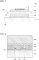
- Fig. 1 shows a power module 1 using an insulating circuit substrate 10 according to the first embodiment of the present invention.
- the bonded body in the present embodiment is a circuit layer 20 in which an aluminum layer 21 as an aluminum member and a copper layer 22 as a copper member are bonded via a titanium layer 25, and a metal layer 30 in which an aluminum layer 31 as an aluminum member and the copper layer 32 as the copper member are bonded via a titanium layer 35.
- the power module 1 shown in Fig. 1 is provided with the insulating circuit substrate 10, a power semiconductor element 3 bonded to one surface (the upper surface in Fig. 1 ) of the insulating circuit substrate 10 via a first solder layer 2, and a heat sink 41 bonded to the lower side of the insulating circuit substrate 10 via a second solder layer 42.
- the insulating circuit substrate 10 to which the heat sink 41 is bonded is an insulating circuit substrate with a heat sink 40 in the present embodiment.
- the power semiconductor element 3 is formed of a semiconductor material such as Si.
- the first solder layer 2 for bonding the insulating circuit substrate 10 and the power semiconductor element 3 is, for example, a Sn-Ag-based, a Sn-Cu-based, a Sn-In-based, or a Sn-Ag-Cu-based solder material (so-called lead-free solder material).
- the heat sink 41 is for radiating heat from the insulating circuit substrate 10 side.
- the heat sink 41 is formed of copper or a copper alloy and is formed of oxygen-free copper in the present embodiment.
- the second solder layer 42 for bonding the insulating circuit substrate 10 and the heat sink 41 is, for example, a Sn-Ag-based, a Sn-Cu-based, a Sn-In-based, or a Sn-Ag-Cu-based solder material (so-called lead-free solder material).
- the insulating circuit substrate 10 is provided with a ceramic substrate 11, the circuit layer 20 arranged on one surface (the upper surface in Fig. 1 ) of the ceramic substrate 11, and the metal layer 30 arranged on the other surface (lower surface in Fig. 1 ) of the ceramic substrate 11.
- the ceramic substrate 11 is formed of AlN (aluminum nitride), Si 3 N 4 (silicon nitride), Al 2 O 3 (alumina), or the like, which have high insulation properties.
- the ceramic substrate 11 is formed of Si 3 N 4 (silicon nitride) having excellent strength.
- the thickness of the ceramic substrate 11 is set in a range of 0.2 to 1.5 mm and is set to 0.32 mm in the present embodiment.
- the circuit layer 20 has the aluminum layer 21 arranged on one surface of the ceramic substrate 11 and the copper layer 22 laminated on one surface of the aluminum layer 21 via the titanium layer 25.
- the thickness of the aluminum layer 21 in the circuit layer 20 is set in a range of 0.1 mm or more and 1.0 mm or less and is set to 0.4 mm in the present embodiment.
- the thickness of the copper layer 22 in the circuit layer 20 is set in a range of 0.1 mm or more and 6.0 mm or less and is set to 1.0 mm in the present embodiment.
- the metal layer 30 has the aluminum layer 31 arranged on the other surface of the ceramic substrate 11 and a copper layer 32 laminated on the other surface of the aluminum layer 31 via the titanium layer 35.
- the thickness of the aluminum layer 31 in the metal layer 30 is set in a range of 0.1 mm or more and 3.0 mm or less and is set to 0.4 mm in the present embodiment.
- the thickness of the copper layer 32 in the metal layer 30 is set in a range of 0.1 mm or more and 6.0 mm or less and is set to 1.0 mm in the present embodiment.
- the aluminum layers 21 and 31 are provided by bonding aluminum sheets 51 and 61 to one surface and the other surface of the ceramic substrate 11.
- the aluminum sheets 51 and 61 to be the aluminum layers 21 and 31 are formed of aluminum (2N aluminum) having a purity of 99 mass% or higher. That is, the Si content is in a range of 0.03 mass% or more and 1.0 mass% or less.
- the copper layers 22 and 32 are provided by bonding copper sheets 52 and 62 formed of copper or a copper alloy to one surface and the other surface of the aluminum layers 21 and 31 via the titanium layers 25 and 35, respectively.
- the copper sheets 52 and 62 forming the copper layers 22 and 32 are oxygen-free copper rolled sheets.
- the aluminum layers 21 and 31 and the titanium layers 25 and 35 and the titanium layers 25 and 35 and the copper layers 22 and 32 are solid phase diffusion bonded, respectively.
- Al-Ti-Si layers 26 and 36 are provided at the bonded interfaces between the aluminum layers 21 and 31 and the titanium layers 25 and 35.
- the Al-Ti-Si layers 26 and 36 are provided by dissolving the Si of the aluminum layers 21 and 31 in Al 3 Ti provided by inter-diffusing the Al atoms of the aluminum layers 21 and 31 and the Ti atoms of the titanium layers 25 and 35.
- the thickness of the Al-Ti-Si layers 26 and 36 is set to 0.5 ⁇ m or more and 10 ⁇ m or less and is 3 ⁇ m in the present embodiment.
- intermetallic compound phases 27 and 37 containing Ti and Cu are provided at the bonded interfaces between the titanium layers 25 and 35 and the copper layers 22 and 32.
- the intermetallic compound phases 27 and 37 are provided by inter-diffusion of Cu atoms in the copper layers 22 and 32 and Ti atoms in the titanium layers 25 and 35.
- intermetallic compound unformed parts 28 and 38 may be present.
- the maximum value of the length L i of the intermetallic compound unformed parts 28 and 38 along the bonded interface is 20 ⁇ m or less.
- the ratio ⁇ L i /L 0 of the total length ⁇ L i of the intermetallic compound unformed parts 28 and 38 along the bonded interface and the total length L 0 of the bonded interface is 0.16 or less.
- the maximum value of the length Li of the observed intermetallic compound unformed parts 28 and 38 along the bonded interface is 20 ⁇ m or less, and the ratio ⁇ L i /L 0 between the total length ⁇ L i of the observed intermetallic compound unformed parts 28 and 38 along the bonded interface and the total length L 0 of the bonded interface in the observation field of view is 0.16 or less.
- an aluminum sheet 51 to be the aluminum layer 21 is laminated, and a copper sheet 52 to be the copper layer 22 is further laminated thereon via a titanium material 55.
- an aluminum sheet 61 to be the aluminum layer 31 is laminated, and a copper sheet 62 to be the copper layer 32 is further laminated thereon via a titanium material 65.
- the aluminum sheets 51 and 61 and the ceramic substrate 11 were laminated via Al-Si based brazing material foils 58 and 68.
- the circuit layer 20 is provided by bonding the aluminum sheet 51 and the ceramic substrate 11 under vacuum conditions by heating in a state of being pressed in a range of 8 kgf/cm 2 or more and 20 kgf/cm 2 or less in the laminating direction, and solid-phase diffusing the aluminum sheet 51 and the titanium material 55 and the titanium material 55 and the copper sheet 52.
- the metal layer 30 is provided by bonding the aluminum sheet 61 and the ceramic substrate 11 and solid-phase diffusing the aluminum sheet 61 and the titanium material 65 and the titanium material 65 and the copper sheet 62.
- the vacuum condition is set in a range of 10 -6 Pa or more and 10 -3 Pa or less
- the heating temperature is set to 630°C or higher and 643°C or lower
- the holding time is set in a range of 210 minutes or more and 360 minutes or less.
- pressing and heating were performed using a hot press device such that the pressing force was in the range described above at the bonding temperature.
- Each of the surfaces of the aluminum sheets 51 and 61, the titanium materials 55 and 65, and the copper sheets 52 and 62 to be bonded are solid-phase diffusion-bonded after scratches on the surfaces are removed and smoothed in advance.
- the insulating circuit substrate 10 of the present embodiment is manufactured as described above.
- the heat sink 41 is laminated on the metal layer 30 of the insulating circuit substrate 10 via a solder material and solder-bonded in a reducing furnace (heat sink bonding step S03).
- the insulating circuit substrate with a heat sink 40 of the present embodiment is manufactured.
- the power semiconductor element 3 is laminated on one surface (the surface of the copper layer 22) of the circuit layer 20 via a solder material and solder-bonded in a reducing furnace (power semiconductor element-bonding step S04).
- the power module 1 of the present embodiment is manufactured as described above.
- the circuit layer 20 has a structure in which the aluminum layer 21, the titanium layer 25, and the copper layer 22 are each solid-phase diffused
- the metal layer 30 has a structure in which the aluminum layer 31, the titanium layer 35, and the copper layer 32 are each solid-phase diffusion bonded, and, at the bonded interface of the copper layers 22 and 32 and the titanium layers 25 and 35, the maximum value of the length L i of the intermetallic compound unformed parts 28 and 38, in which the intermetallic compound phases 27 and 37 containing Cu and Ti are not formed, along the bonded interface is 20 ⁇ m or less, thus, Cu and Ti are sufficiently inter-diffused between the copper layers 22 and 32 and the titanium layers 25 and 35 and the bonding reliability between the copper layers 22 and 32 and the titanium layers 25 and 35 is excellent.
- the ratio ⁇ L i /L 0 of the total length ⁇ L i of the intermetallic compound unformed parts 28 and 38 along the bonded interface and the total length L 0 of the bonded interface is 0.16 or less, thus, the ratio of the presence of the intermetallic compound unformed parts 28 and 38 is small and it is possible to suppress peeling from occurring with the intermetallic compound unformed parts 28 and 38 as a starting point even in a case of being subjected to a thermal cycle load at a high temperature.
- the bonding reliability between the copper layer 22 and the titanium layer 25 in the circuit layer 20 is excellent, even when the power semiconductor element 3 having a high heat generation density is mounted on the circuit layer 20, it is possible to suppress peeling from occurring at the bonded interface of the copper layer 22 and the titanium layer 25.
- the bonding reliability between the copper layer 32 and the titanium layer 35 in the metal layer 30 is excellent, it is possible to efficiently radiate the heat from the power semiconductor element 3 mounted on the circuit layer 20 to the heat sink 41 side via the metal layer 30.
- the aluminum layers 21 and 31 having a relatively small deformation resistance are formed on one surface and the other surface of the ceramic substrate 11, it is possible to absorb the thermal stress generated when subjected to a thermal cycle load by the deformation of the aluminum layers 21 and 31 and to suppress the generation of fractures in the ceramic substrate 11.
- the copper layers 22 and 32 having relatively large deformation resistance are provided on the surface on the opposite side to the surface of the aluminum layers 21 and 31 on which the ceramic substrate 11 is provided, when subjected to a thermal cycle load, deformation of the surface of the circuit layer 20 and the metal layer 30 is suppressed, it is possible to suppress the generation of fractures in the first solder layer 2 for bonding the circuit layer 20 and the power semiconductor element 3 and the second solder layer 42 for bonding the metal layer 30 and the heat sink 41, and to improve the bonding reliability.
- the present embodiment has a configuration in which the ceramic substrate 11, the aluminum sheets 51 and 61, the titanium materials 55 and 65, and the copper sheets 52 and 62 are bonded in a batch, thus, it is possible to simplify the manufacturing steps and to reduce manufacturing costs.
- the present embodiment has a configuration in which the solid-phase diffusion bonding of the aluminum sheets 51 and 61, the titanium materials 55 and 65, and the copper sheets 52 and 62 is performed by maintaining a temperature at 630°C or higher and 643°C or lower in a state where a pressure of 8 to 20 kgf/cm 2 is applied in the laminating direction, Al atoms and Ti atoms and Ti atoms and Cu atoms are inter-diffused and Al atoms and Cu atoms are solid phase diffused in the titanium material 25 to carry out solid phase diffusion bonding, and it is possible to reliably bond the aluminum sheets 51 and 61, the titanium materials 55 and 65, and the copper sheets 52 and 62.
- Fig. 5 shows a power module 101 using an insulating circuit substrate with a heat sink 140 according to a second embodiment of the present invention.
- the same members as in the first embodiment are designated by the same reference numerals and detailed description thereof will be omitted.
- the metal layer 130 which is an aluminum member and a heat sink 141 which is a copper member are bonded via a titanium layer 145.
- the power module 101 shown in Fig. 5 is provided with the insulating circuit substrate with a heat sink 140 and the power semiconductor element 3 bonded to one surface (the upper surface in Fig. 5 ) of the insulating circuit substrate with a heat sink 140 via the first solder layer 2.
- the insulating circuit substrate with a heat sink 140 of the present embodiment is provided with an insulating circuit substrate 110 and the heat sink 141 bonded to the metal layer 130 of the insulating circuit substrate 110.
- the heat sink 141 is for radiating heat from the insulating circuit substrate 110 side.
- the heat sink 141 is formed of copper or a copper alloy and is formed of oxygen-free copper in the present embodiment.
- the insulating circuit substrate 110 is provided with the ceramic substrate 11, a circuit layer 120 arranged on one surface (the upper surface in Fig. 5 ) of the ceramic substrate 11, and a metal layer 130 arranged on the other surface (the lower surface in Fig. 5 ) of the ceramic substrate 11.
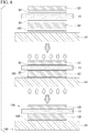
- the circuit layer 120 is provided by bonding an aluminum sheet 151 formed of aluminum or an aluminum alloy to one surface (the upper surface in Fig. 8 ) of the ceramic substrate 11 as shown in Fig. 8 .
- the circuit layer 120 is provided by bonding a rolled sheet of aluminum (2N aluminum) having a purity of 99% or more to the ceramic substrate 11.
- the thickness of the aluminum sheet 151 to be the circuit layer 120 is set in a range of 0.1 mm or more and 1.0 mm or less and is set to 0.6 mm in the present embodiment.
- the metal layer 130 is provided by bonding an aluminum sheet 161 to the other surface (the lower surface in Fig. 8 ) of the ceramic substrate 11 as shown in Fig. 8 .
- the aluminum sheet 161 forming the metal layer 130 is a rolled sheet of aluminum (4N aluminum) having a purity of 99.99% by mass or more.
- the thickness of the aluminum sheet 161 to be bonded is set in a range of 0.1 mm or more and 3.0 mm or less and is set to 0.6 mm in the present embodiment.
- the metal layer 130 and the heat sink 141 are bonded via the titanium layer 145.
- the metal layer 130 and the titanium layer 145, and the titanium layer 145 and the heat sink 141 are each solid phase diffusion bonded.
- an Al-Ti-Si layer 146 is provided at the bonded interface of the metal layer 130 and the titanium layer 145, as shown in Fig. 6 .
- the Al-Ti-Si layer 146 is provided by solid-dissolving Si of the metal layer 130 in Al 3 Ti provided by inter-diffusion of Al atoms of the metal layer 130 and Ti atoms of the titanium layer 145.
- the thickness of the Al-Ti-Si layer 146 is set to 0.5 ⁇ m or more and 10 ⁇ m or less and is 3 ⁇ m in the present embodiment.
- an intermetallic compound phase 147 containing Ti and Cu is formed at the bonded interface of the titanium layer 145 and the heat sink 141.
- the intermetallic compound phase 147 is provided by mutual diffusion of Cu atoms of the heat sink 141 and Ti atoms of the titanium layer 145.
- an intermetallic compound unformed part 148) may be present.
- the maximum value of the length L i of the intermetallic compound unformed part 148 along the bonded interface is 20 ⁇ m or less.
- the ratio ⁇ L i /L 0 of the total length ⁇ L i of the intermetallic compound unformed part 148 along the bonded interface and the total length L 0 of the bonded interface in the observation field of view is 0.16 or less.
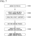
- the aluminum sheet 151 to be the circuit layer 120 is laminated on one surface (the upper surface in Fig. 8 ) of the ceramic substrate 11, and the aluminum sheet 161 to be the metal layer 130 is laminated on the other surface (the lower surface in Fig. 8 ) of the ceramic substrate 11.
- the heat sink 141 is laminated on the other surface side of the aluminum sheet 161 to be the metal layer 130 via a titanium material 165 (laminating step S101).
- the aluminum sheets 151 and 161 and the ceramic substrate 11 were laminated via the Al-Si type brazing material foils 58 and 68.
- the aluminum sheet 151 and the ceramic substrate 11 are bonded by heating in a state of being pressed in a range of 8 kgf/cm 2 or more and 20 kgf/cm 2 or less in the laminating direction, and the circuit layer 120 is provided.
- the aluminum sheet 161 and the ceramic substrate 11 are bonded to provide the metal layer 130. (Circuit layer and metal layer providing step S102).
- the aluminum sheet 161 and the titanium material 165, and the titanium material 165 and the heat sink 141 are solid-phase diffusion bonded (heat sink bonding step S103).
- the vacuum condition is set in a range of 10 -6 Pa or more and 10 -3 Pa or less
- the heating temperature is set to 630°C or higher and 643°C or lower
- the holding time is set in a range of 210 minutes or more and 360 minutes or less.
- pressing and heating were performed using a hot press device such that the pressing force was in the range described above at the bonding temperature.
- the respective bonding surfaces of the aluminum sheet 161, the titanium material 165, and the heat sink 141 are solid-phase diffusion bonded after the scratches on the surfaces were removed and smoothed in advance.
- the insulating circuit substrate with a heat sink 140 of the present embodiment is manufactured as described above.
- the power semiconductor element 3 is laminated on one surface of the circuit layer 120 of the insulating circuit substrate 110 via a solder material and solder bonded in a reducing furnace (power semiconductor element-bonding step S104).
- the power module 101 of the present embodiment is manufactured as described above.
- the insulating circuit substrate with a heat sink 140 of the present embodiment configured as described above has a structure in which the metal layer 130 which is an aluminum member and the titanium layer 145, and the titanium layer 145 and the heat sink 141 which is a copper member are respectively solid phase diffusion bonded, and, at the bonded interface of the heat sink 141 and the titanium layer 145, the maximum value of the length L i of the intermetallic compound unformed part 148 where the intermetallic compound phase 147 containing Cu and Ti is not formed along the bonded interface is 20 ⁇ m or less, thus, Cu and Ti are sufficiently inter-diffused between the heat sink 141 and the titanium layer 145 and the bonding reliability between the heat sink 141 and the titanium layer 145 is excellent.
- the ratio ⁇ L i /L 0 of the total length ⁇ L i of the intermetallic compound unformed part 148 along the bonded interface and the total length L 0 of the bonded interface is 0.16 or less, thus, the ratio of the presence of the intermetallic compound unformed part 148 is small, and it is possible to suppress peeling from occurring with the intermetallic compound unformed part 148 as a starting point even in a case of being subjected to a thermal cycle load at a high temperature.
- the metal layer 130 which is an aluminum member and the heat sink 141 which is a copper member are bonded via the titanium layer 145 and the bonding reliability between the heat sink 141 and the titanium layer 145 is excellent, thus, even in a case of being subjected to a thermal cycle load at a high temperature, it is possible to suppress the generation of peeling at the bonded interface of the heat sink 141 and the titanium layer 145, and to efficiently radiateheat from the power semiconductor element 3 mounted on the circuit layer 120 to the heat sink 141 side via the metal layer 130.
- thermoelectric element may be mounted on a circuit layer of an insulating circuit substrate to form a thermoelectric module.
- a circuit layer 220 may be configured by a copper/titanium/aluminum bonded body obtained by bonding, via a titanium layer 225, a copper member (copper layer 222) formed of copper or a copper alloy and an aluminum member (aluminum layer 221) formed of aluminum or an aluminum alloy.
- a metal layer 330 may be configured by the copper/titanium/aluminum bonded body obtained by bonding, via a titanium layer 335, a copper member (copper layer 332) formed of copper or a copper alloy and an aluminum member (aluminum layer 331) formed of aluminum or an aluminum alloy.
- the present invention is not limited thereto and it is sufficient to have a copper/titanium/aluminum bonded body with a structure in which the titanium layer and the copper layer are solid-phase diffusion bonded and in which an intermetallic compound containing Cu and Ti is formed at the bonded interface of the titanium layer and the copper layer.
- an aluminum sheet (37 mm ⁇ 37 mm ⁇ 0.6 mmt) formed of aluminum (2N aluminum) having a purity of 99 mass% or more, a titanium material (37 mm ⁇ 37 mm ⁇ 0.020 mmt), and a Cu sheet (37 mm ⁇ 37 mm ⁇ 0.3 mmt) shown in Table 1 were laminated in this order via a brazing material foil (thickness 10 ⁇ m) formed of Al-7 mass% Si alloy to obtain a laminated body.
- the laminated body described above was heated in a state of being pressed in the laminating direction at a pressure shown in Table 1 using a hot press device.
- the bonding conditions were the conditions shown in Table 1. In this manner, the insulating circuit substrates of Examples 1 to 10 of the present invention and Comparative Examples 1 to 3 were obtained.
- the ceramic substrate of the Examples 1 to 10 of the present invention and the Comparative Examples 1 to 3, the brazing material foil, the aluminum sheet, the titanium material, and the Cu sheet shown in Table 1 were laminated in order to obtain a laminated body S. Then, as shown in Fig. 11 , the laminated body S described above was pressed using a pressing jig 400 formed of stainless steel and loaded into a vacuum heating furnace.
- the pressing jig 400 is provided with a base plate 401, guide posts 402 vertically attached to the four corners of the upper surface of the base plate 401, a fixing plate 403 fixed to upper end portions of the guide posts 402, a pressing plate 404 supported by the guide posts 402 so as to be freely vertically movable between the base plate 401 and the fixing plate 403, and an urging means 405, such as a spring, urging the pressing plate 404 downward and provided between the fixing plate 403 and the pressing plate 404, in which the laminated body S described above is arranged between the base plate 401 and the pressing plate 404.
- the pressing force at the heating temperature is lower than the conditions shown in Table 1 due to the thermal expansion of the guide post 402 and the like of the pressing jig 400.
- the bonded interface of the copper layer and the titanium layer was observed and the length Li of the intermetallic compound unformed part along the bonded interface and the ratio L i /L 0 of the length L i and the total length L 0 of the bonded interface in the observation field of view were measured.
- the cross-section of the insulating circuit substrate was observed using EPMA (JXA-8539F manufactured by JEOL Ltd.), the elemental MAP of Cu and Ti in a region (100 ⁇ m in length ⁇ 200 ⁇ m in width) including a bonded interface of a copper layer and a titanium layer was acquired, a region where the Cu concentration was 5 at% or more and the Ti concentration was 16 at% or more and 70 at% or less was set as the intermetallic compound phase, and a region between the intermetallic compound phases at the bonded interface was set as the length L i of the intermetallic compound unformed part along the bonded interface.
- EPMA JXA-8539F manufactured by JEOL Ltd.
- TSA-72ES Thermal shock tester manufactured by ESPEC Corp.
- 1000 cycles were carried out on the insulating circuit substrate in a gas phase at -40°C for 5 minutes and at 175°C for 5 minutes.
- the bonding rate between the copper layer and the titanium layer was evaluated as follows. The bonding rate was evaluated before the thermal cycle test (initial bonding rate) and after the thermal cycle test (post-cycle bonding rate).
- the bonding rate was evaluated using an ultrasonic flaw detector (FineSAT200 manufactured by Hitachi Power Solutions Co., Ltd.) for the bonding rate at the interface between the copper layer and the titanium layer on the insulating circuit substrate, and the bonding rate was calculated from the equation below.
- FineSAT200 manufactured by Hitachi Power Solutions Co., Ltd.
- the initial bonding area is the area to be bonded before bonding, that is, the area (37 mm ⁇ 37 mm) of the circuit layer and the metal layer in the present embodiment.
- Bonding rate Initial bonding area ⁇ exfoliation area / Initial bonding area ⁇ 100
- the peeling was indicated by the white portion inside the bonded portion such that the area of this white portion was defined as the exfoliationarea.
- the bonding temperature was set as low as 620°C
- the intermetallic compound unformed part length Li was 37 ⁇ m, which was larger than the range of the present invention
- the length ratio ⁇ Li/L0 described above was 0.25, which was larger than the range of the present invention. Due to this, the bonding rate after the thermal cycle test was lowered to 86.5%.
- Comparative Example 2 the holding time at the bonding temperature was set to be short at 60 min and the length ratio ⁇ Li/L0 described above was 0.28, which was larger than the range of the present invention. Due to this, the bonding rate after the thermal cycle test was lowered to 85.7%.
- the pressure load was set to be low at 5 kgf/cm 2 and the intermetallic compound unformed part length Li was 31 ⁇ m, which was larger than the range of the present invention. Due to this, the bonding rate after the thermal cycle test was lowered to 87.4%.
- a copper/titanium/aluminum bonded body in which it is possible to suppress peeling from occurring at a bonded interface of a copper member and a titanium layer even in a case of being subjected to a thermal cycle load at a temperature higher than in the related art and in which the reliability is particularly excellent, as well as an insulating circuit substrate, an insulating circuit substrate with a heat sink, a power module, an LED module, and a thermoelectric module, which are provided with the same.
Landscapes
- Engineering & Computer Science (AREA)
- Mechanical Engineering (AREA)
- Cooling Or The Like Of Semiconductors Or Solid State Devices (AREA)
- Chemical & Material Sciences (AREA)
- Ceramic Engineering (AREA)
- Materials Engineering (AREA)
- Laminated Bodies (AREA)
Applications Claiming Priority (1)
| Application Number | Priority Date | Filing Date | Title |
|---|---|---|---|
| PCT/JP2018/004835 WO2019159219A1 (ja) | 2018-02-13 | 2018-02-13 | 銅/チタン/アルミニウム接合体、絶縁回路基板、ヒートシンク付き絶縁回路基板、パワーモジュール、ledモジュール、熱電モジュール |
Publications (3)
| Publication Number | Publication Date |
|---|---|
| EP3754701A1 true EP3754701A1 (de) | 2020-12-23 |
| EP3754701A4 EP3754701A4 (de) | 2021-08-25 |
| EP3754701B1 EP3754701B1 (de) | 2022-06-08 |
Family
ID=67619223
Family Applications (1)
| Application Number | Title | Priority Date | Filing Date |
|---|---|---|---|
| EP18906230.0A Active EP3754701B1 (de) | 2018-02-13 | 2018-02-13 | Kupfer/titan/aluminium-verbindung, isolierende leiterplatte, isolierende leiterplatte mit kühlkörper, leistungsmodul, led-modul und thermoelektrisches modul |
Country Status (5)
| Country | Link |
|---|---|
| US (1) | US11887909B2 (de) |
| EP (1) | EP3754701B1 (de) |
| KR (1) | KR102363709B1 (de) |
| CN (1) | CN111656518B (de) |
| WO (1) | WO2019159219A1 (de) |
Family Cites Families (22)
| Publication number | Priority date | Publication date | Assignee | Title |
|---|---|---|---|---|
| FR2291803A1 (fr) | 1974-11-20 | 1976-06-18 | Alsthom Cgee | Perfectionnements aux generateurs a houle du type a plongeur |
| JP2861357B2 (ja) | 1990-10-17 | 1999-02-24 | 株式会社村田製作所 | 窒化アルミニウム―銅接合方法 |
| JP2999760B2 (ja) | 1998-02-05 | 2000-01-17 | 日本碍子株式会社 | ベリリウムと銅合金のhip接合体の製造方法およびhip接合体 |
| JP2004231513A (ja) | 2000-10-26 | 2004-08-19 | Hitachi Metals Ltd | 高強度・高熱伝導性に優れた回路基板 |
| US8342386B2 (en) * | 2006-12-15 | 2013-01-01 | General Electric Company | Braze materials and processes therefor |
| JP2013038330A (ja) * | 2011-08-10 | 2013-02-21 | Toshiba Corp | 半導体装置の製造方法及び半導体装置 |
| US9968012B2 (en) * | 2012-10-16 | 2018-05-08 | Mitsubishi Materials Corporation | Heat-sink-attached power module substrate, heat-sink-attached power module, and method for producing heat-sink-attached power module substrate |
| JP5725061B2 (ja) | 2013-03-14 | 2015-05-27 | 三菱マテリアル株式会社 | パワーモジュール用基板、及びヒートシンク付パワーモジュール用基板 |
| JP5725060B2 (ja) | 2013-03-14 | 2015-05-27 | 三菱マテリアル株式会社 | 接合体、パワーモジュール用基板、及びヒートシンク付パワーモジュール用基板 |
| JP6018297B2 (ja) * | 2013-04-26 | 2016-11-02 | 京セラ株式会社 | 複合積層体および電子装置 |
| EP3041045B1 (de) | 2013-08-26 | 2019-09-18 | Mitsubishi Materials Corporation | Verbundkörper und leistungsmodulsubstrat |
| JP6079505B2 (ja) | 2013-08-26 | 2017-02-15 | 三菱マテリアル株式会社 | 接合体及びパワーモジュール用基板 |
| JP6432208B2 (ja) * | 2014-08-18 | 2018-12-05 | 三菱マテリアル株式会社 | パワーモジュール用基板の製造方法、及び、ヒートシンク付パワーモジュール用基板の製造方法 |
| JP6432465B2 (ja) * | 2014-08-26 | 2018-12-05 | 三菱マテリアル株式会社 | 接合体、ヒートシンク付パワーモジュール用基板、ヒートシンク、接合体の製造方法、ヒートシンク付パワーモジュール用基板の製造方法、及び、ヒートシンクの製造方法 |
| JP6432466B2 (ja) | 2014-08-26 | 2018-12-05 | 三菱マテリアル株式会社 | 接合体、ヒートシンク付パワーモジュール用基板、ヒートシンク、接合体の製造方法、ヒートシンク付パワーモジュール用基板の製造方法、及び、ヒートシンクの製造方法 |
| JP6456676B2 (ja) * | 2014-09-10 | 2019-01-23 | Jx金属株式会社 | 金属セラミック接合基板及び、その製造方法 |
| KR102129339B1 (ko) * | 2016-06-10 | 2020-07-03 | 다나카 기킨조쿠 고교 가부시키가이샤 | 세라믹스 회로 기판, 및 세라믹스 회로 기판의 제조 방법 |
| JP2017224656A (ja) * | 2016-06-13 | 2017-12-21 | Ngkエレクトロデバイス株式会社 | 金属−セラミックス複合基板および半導体装置 |
| JP6645368B2 (ja) * | 2016-06-23 | 2020-02-14 | 三菱マテリアル株式会社 | 接合体、パワーモジュール用基板、接合体の製造方法、及び、パワーモジュール用基板の製造方法 |
| JP6904088B2 (ja) * | 2016-06-30 | 2021-07-14 | 三菱マテリアル株式会社 | 銅/セラミックス接合体、及び、絶縁回路基板 |
| JP6729225B2 (ja) * | 2016-09-13 | 2020-07-22 | 三菱マテリアル株式会社 | 銅/チタン/アルミニウム接合体、絶縁回路基板、ヒートシンク付き絶縁回路基板、パワーモジュール、ledモジュール、熱電モジュール |
| JP6621068B2 (ja) * | 2016-12-08 | 2019-12-18 | パナソニックIpマネジメント株式会社 | 実装構造体 |
-
2018
- 2018-02-13 US US16/959,160 patent/US11887909B2/en active Active
- 2018-02-13 KR KR1020207021420A patent/KR102363709B1/ko not_active Expired - Fee Related
- 2018-02-13 CN CN201880087807.XA patent/CN111656518B/zh active Active
- 2018-02-13 WO PCT/JP2018/004835 patent/WO2019159219A1/ja not_active Ceased
- 2018-02-13 EP EP18906230.0A patent/EP3754701B1/de active Active
Also Published As
| Publication number | Publication date |
|---|---|
| EP3754701A4 (de) | 2021-08-25 |
| KR102363709B1 (ko) | 2022-02-15 |
| US20200343158A1 (en) | 2020-10-29 |
| WO2019159219A1 (ja) | 2019-08-22 |
| US11887909B2 (en) | 2024-01-30 |
| CN111656518A (zh) | 2020-09-11 |
| KR20200120618A (ko) | 2020-10-21 |
| EP3754701B1 (de) | 2022-06-08 |
| CN111656518B (zh) | 2023-05-16 |
Similar Documents
| Publication | Publication Date | Title |
|---|---|---|
| CN109417056B (zh) | 铜-陶瓷接合体及绝缘电路基板 | |
| EP2911192B1 (de) | Substrat für ein strommodul mit einem kühlkörper, strommodul mit einem kühlkörper und verfahren zur herstellung des substrats für das strommodul mit einem kühlkörper | |
| EP2978018B1 (de) | Verfahren zur herstellung eines strommodulsubstrats | |
| EP2950340B1 (de) | Leistungsmodulsubstrat, leistungsmodulsubstrat mit kühlkörper und leistungsmodul mit kühlkörper | |
| EP2978019B1 (de) | Verfahren zur herstellung eines verbundeten körpers und verfahren zur herstellung eines strommodulsubstrats | |
| EP2980844A1 (de) | Substrat für leistungsmodule, substrat mit kühlkörper für leistungsmodule und leistungsmodul | |
| EP2940719B1 (de) | Leistungsmodul | |
| EP3106447B1 (de) | Kupfer-keramik verbundkörper und leistungsmodulsubstrat | |
| EP2980843B1 (de) | Leistungsmodul | |
| CN114845977A (zh) | 铜-陶瓷接合体、及绝缘电路基板 | |
| CN114342573B (zh) | 铜-陶瓷接合体及绝缘电路基板 | |
| EP3845511B1 (de) | Kupfer-keramik-fügekörper, isolierte leiterplatte, verfahren zur herstellung eines kupfer-keramik-fügekörpers sowie verfahren zur herstellung einer isolierten leiterplatte | |
| JP2021095327A (ja) | 銅/セラミックス接合体、及び、絶縁回路基板 | |
| JP6645368B2 (ja) | 接合体、パワーモジュール用基板、接合体の製造方法、及び、パワーモジュール用基板の製造方法 | |
| EP3754701B1 (de) | Kupfer/titan/aluminium-verbindung, isolierende leiterplatte, isolierende leiterplatte mit kühlkörper, leistungsmodul, led-modul und thermoelektrisches modul | |
| JP6729225B2 (ja) | 銅/チタン/アルミニウム接合体、絶縁回路基板、ヒートシンク付き絶縁回路基板、パワーモジュール、ledモジュール、熱電モジュール | |
| WO2022224949A1 (ja) | 銅/セラミックス接合体、および、絶縁回路基板 | |
| JP7725907B2 (ja) | 銅/セラミックス接合体、および、絶縁回路基板 | |
| JP7676903B2 (ja) | 銅/セラミックス接合体、および、絶縁回路基板 | |
| EP4447624A1 (de) | Kupfer/keramik verbundkörper und isolierte leiterplatte | |
| JP2021031315A (ja) | 銅/セラミックス接合体、絶縁回路基板、及び、銅/セラミックス接合体の製造方法、絶縁回路基板の製造方法 | |
| EP4159704B1 (de) | Kupfer/keramik-verbundkörper und isoliertes schaltungssubstrat | |
| JP2022165044A (ja) | 銅/セラミックス接合体、および、絶縁回路基板 | |
| TW201935623A (zh) | 銅鈦鋁接合體、絕緣電路基板、附散熱塊絕緣電路基板、功率模組、led模組、熱電模組 |
Legal Events
| Date | Code | Title | Description |
|---|---|---|---|
| STAA | Information on the status of an ep patent application or granted ep patent |
Free format text: STATUS: THE INTERNATIONAL PUBLICATION HAS BEEN MADE |
|
| PUAI | Public reference made under article 153(3) epc to a published international application that has entered the european phase |
Free format text: ORIGINAL CODE: 0009012 |
|
| STAA | Information on the status of an ep patent application or granted ep patent |
Free format text: STATUS: REQUEST FOR EXAMINATION WAS MADE |
|
| 17P | Request for examination filed |
Effective date: 20200626 |
|
| AK | Designated contracting states |
Kind code of ref document: A1 Designated state(s): AL AT BE BG CH CY CZ DE DK EE ES FI FR GB GR HR HU IE IS IT LI LT LU LV MC MK MT NL NO PL PT RO RS SE SI SK SM TR |
|
| AX | Request for extension of the european patent |
Extension state: BA ME |
|
| DAV | Request for validation of the european patent (deleted) | ||
| DAX | Request for extension of the european patent (deleted) | ||
| A4 | Supplementary search report drawn up and despatched |
Effective date: 20210728 |
|
| RIC1 | Information provided on ipc code assigned before grant |
Ipc: H01L 23/36 20060101AFI20210722BHEP Ipc: B23K 20/00 20060101ALI20210722BHEP Ipc: B32B 15/04 20060101ALI20210722BHEP Ipc: B32B 15/20 20060101ALI20210722BHEP Ipc: H01L 23/373 20060101ALI20210722BHEP Ipc: H01L 21/48 20060101ALI20210722BHEP Ipc: H01L 35/32 20060101ALI20210722BHEP Ipc: H01L 21/64 20060101ALN20210722BHEP Ipc: H01L 23/498 20060101ALN20210722BHEP |
|
| GRAP | Despatch of communication of intention to grant a patent |
Free format text: ORIGINAL CODE: EPIDOSNIGR1 |
|
| STAA | Information on the status of an ep patent application or granted ep patent |
Free format text: STATUS: GRANT OF PATENT IS INTENDED |
|
| RIC1 | Information provided on ipc code assigned before grant |
Ipc: H01L 23/498 20060101ALN20220214BHEP Ipc: H01L 21/64 20060101ALN20220214BHEP Ipc: H01L 35/32 20060101ALI20220214BHEP Ipc: H01L 21/48 20060101ALI20220214BHEP Ipc: H01L 23/373 20060101ALI20220214BHEP Ipc: B32B 15/20 20060101ALI20220214BHEP Ipc: B32B 15/04 20060101ALI20220214BHEP Ipc: B23K 20/00 20060101ALI20220214BHEP Ipc: H01L 23/36 20060101AFI20220214BHEP |
|
| INTG | Intention to grant announced |
Effective date: 20220310 |
|
| GRAS | Grant fee paid |
Free format text: ORIGINAL CODE: EPIDOSNIGR3 |
|
| GRAA | (expected) grant |
Free format text: ORIGINAL CODE: 0009210 |
|
| STAA | Information on the status of an ep patent application or granted ep patent |
Free format text: STATUS: THE PATENT HAS BEEN GRANTED |
|
| AK | Designated contracting states |
Kind code of ref document: B1 Designated state(s): AL AT BE BG CH CY CZ DE DK EE ES FI FR GB GR HR HU IE IS IT LI LT LU LV MC MK MT NL NO PL PT RO RS SE SI SK SM TR |
|
| REG | Reference to a national code |
Ref country code: AT Ref legal event code: REF Ref document number: 1497516 Country of ref document: AT Kind code of ref document: T Effective date: 20220615 Ref country code: CH Ref legal event code: EP |
|
| REG | Reference to a national code |
Ref country code: DE Ref legal event code: R096 Ref document number: 602018036650 Country of ref document: DE |
|
| REG | Reference to a national code |
Ref country code: IE Ref legal event code: FG4D |
|
| REG | Reference to a national code |
Ref country code: LT Ref legal event code: MG9D |
|
| REG | Reference to a national code |
Ref country code: NL Ref legal event code: MP Effective date: 20220608 |
|
| PG25 | Lapsed in a contracting state [announced via postgrant information from national office to epo] |
Ref country code: SE Free format text: LAPSE BECAUSE OF FAILURE TO SUBMIT A TRANSLATION OF THE DESCRIPTION OR TO PAY THE FEE WITHIN THE PRESCRIBED TIME-LIMIT Effective date: 20220608 Ref country code: NO Free format text: LAPSE BECAUSE OF FAILURE TO SUBMIT A TRANSLATION OF THE DESCRIPTION OR TO PAY THE FEE WITHIN THE PRESCRIBED TIME-LIMIT Effective date: 20220908 Ref country code: LT Free format text: LAPSE BECAUSE OF FAILURE TO SUBMIT A TRANSLATION OF THE DESCRIPTION OR TO PAY THE FEE WITHIN THE PRESCRIBED TIME-LIMIT Effective date: 20220608 Ref country code: HR Free format text: LAPSE BECAUSE OF FAILURE TO SUBMIT A TRANSLATION OF THE DESCRIPTION OR TO PAY THE FEE WITHIN THE PRESCRIBED TIME-LIMIT Effective date: 20220608 Ref country code: GR Free format text: LAPSE BECAUSE OF FAILURE TO SUBMIT A TRANSLATION OF THE DESCRIPTION OR TO PAY THE FEE WITHIN THE PRESCRIBED TIME-LIMIT Effective date: 20220909 Ref country code: FI Free format text: LAPSE BECAUSE OF FAILURE TO SUBMIT A TRANSLATION OF THE DESCRIPTION OR TO PAY THE FEE WITHIN THE PRESCRIBED TIME-LIMIT Effective date: 20220608 Ref country code: BG Free format text: LAPSE BECAUSE OF FAILURE TO SUBMIT A TRANSLATION OF THE DESCRIPTION OR TO PAY THE FEE WITHIN THE PRESCRIBED TIME-LIMIT Effective date: 20220908 |
|
| REG | Reference to a national code |
Ref country code: AT Ref legal event code: MK05 Ref document number: 1497516 Country of ref document: AT Kind code of ref document: T Effective date: 20220608 |
|
| PG25 | Lapsed in a contracting state [announced via postgrant information from national office to epo] |
Ref country code: RS Free format text: LAPSE BECAUSE OF FAILURE TO SUBMIT A TRANSLATION OF THE DESCRIPTION OR TO PAY THE FEE WITHIN THE PRESCRIBED TIME-LIMIT Effective date: 20220608 Ref country code: LV Free format text: LAPSE BECAUSE OF FAILURE TO SUBMIT A TRANSLATION OF THE DESCRIPTION OR TO PAY THE FEE WITHIN THE PRESCRIBED TIME-LIMIT Effective date: 20220608 |
|
| PG25 | Lapsed in a contracting state [announced via postgrant information from national office to epo] |
Ref country code: NL Free format text: LAPSE BECAUSE OF FAILURE TO SUBMIT A TRANSLATION OF THE DESCRIPTION OR TO PAY THE FEE WITHIN THE PRESCRIBED TIME-LIMIT Effective date: 20220608 |
|
| PG25 | Lapsed in a contracting state [announced via postgrant information from national office to epo] |
Ref country code: SM Free format text: LAPSE BECAUSE OF FAILURE TO SUBMIT A TRANSLATION OF THE DESCRIPTION OR TO PAY THE FEE WITHIN THE PRESCRIBED TIME-LIMIT Effective date: 20220608 Ref country code: SK Free format text: LAPSE BECAUSE OF FAILURE TO SUBMIT A TRANSLATION OF THE DESCRIPTION OR TO PAY THE FEE WITHIN THE PRESCRIBED TIME-LIMIT Effective date: 20220608 Ref country code: RO Free format text: LAPSE BECAUSE OF FAILURE TO SUBMIT A TRANSLATION OF THE DESCRIPTION OR TO PAY THE FEE WITHIN THE PRESCRIBED TIME-LIMIT Effective date: 20220608 Ref country code: PT Free format text: LAPSE BECAUSE OF FAILURE TO SUBMIT A TRANSLATION OF THE DESCRIPTION OR TO PAY THE FEE WITHIN THE PRESCRIBED TIME-LIMIT Effective date: 20221010 Ref country code: ES Free format text: LAPSE BECAUSE OF FAILURE TO SUBMIT A TRANSLATION OF THE DESCRIPTION OR TO PAY THE FEE WITHIN THE PRESCRIBED TIME-LIMIT Effective date: 20220608 Ref country code: EE Free format text: LAPSE BECAUSE OF FAILURE TO SUBMIT A TRANSLATION OF THE DESCRIPTION OR TO PAY THE FEE WITHIN THE PRESCRIBED TIME-LIMIT Effective date: 20220608 Ref country code: CZ Free format text: LAPSE BECAUSE OF FAILURE TO SUBMIT A TRANSLATION OF THE DESCRIPTION OR TO PAY THE FEE WITHIN THE PRESCRIBED TIME-LIMIT Effective date: 20220608 Ref country code: AT Free format text: LAPSE BECAUSE OF FAILURE TO SUBMIT A TRANSLATION OF THE DESCRIPTION OR TO PAY THE FEE WITHIN THE PRESCRIBED TIME-LIMIT Effective date: 20220608 |
|
| PG25 | Lapsed in a contracting state [announced via postgrant information from national office to epo] |
Ref country code: PL Free format text: LAPSE BECAUSE OF FAILURE TO SUBMIT A TRANSLATION OF THE DESCRIPTION OR TO PAY THE FEE WITHIN THE PRESCRIBED TIME-LIMIT Effective date: 20220608 Ref country code: IS Free format text: LAPSE BECAUSE OF FAILURE TO SUBMIT A TRANSLATION OF THE DESCRIPTION OR TO PAY THE FEE WITHIN THE PRESCRIBED TIME-LIMIT Effective date: 20221008 |
|
| REG | Reference to a national code |
Ref country code: DE Ref legal event code: R097 Ref document number: 602018036650 Country of ref document: DE |
|
| PG25 | Lapsed in a contracting state [announced via postgrant information from national office to epo] |
Ref country code: AL Free format text: LAPSE BECAUSE OF FAILURE TO SUBMIT A TRANSLATION OF THE DESCRIPTION OR TO PAY THE FEE WITHIN THE PRESCRIBED TIME-LIMIT Effective date: 20220608 |
|
| PLBE | No opposition filed within time limit |
Free format text: ORIGINAL CODE: 0009261 |
|
| STAA | Information on the status of an ep patent application or granted ep patent |
Free format text: STATUS: NO OPPOSITION FILED WITHIN TIME LIMIT |
|
| PG25 | Lapsed in a contracting state [announced via postgrant information from national office to epo] |
Ref country code: DK Free format text: LAPSE BECAUSE OF FAILURE TO SUBMIT A TRANSLATION OF THE DESCRIPTION OR TO PAY THE FEE WITHIN THE PRESCRIBED TIME-LIMIT Effective date: 20220608 |
|
| 26N | No opposition filed |
Effective date: 20230310 |
|
| PG25 | Lapsed in a contracting state [announced via postgrant information from national office to epo] |
Ref country code: SI Free format text: LAPSE BECAUSE OF FAILURE TO SUBMIT A TRANSLATION OF THE DESCRIPTION OR TO PAY THE FEE WITHIN THE PRESCRIBED TIME-LIMIT Effective date: 20220608 |
|
| PG25 | Lapsed in a contracting state [announced via postgrant information from national office to epo] |
Ref country code: MC Free format text: LAPSE BECAUSE OF FAILURE TO SUBMIT A TRANSLATION OF THE DESCRIPTION OR TO PAY THE FEE WITHIN THE PRESCRIBED TIME-LIMIT Effective date: 20220608 |
|
| REG | Reference to a national code |
Ref country code: BE Ref legal event code: MM Effective date: 20230228 |
|
| PG25 | Lapsed in a contracting state [announced via postgrant information from national office to epo] |
Ref country code: LU Free format text: LAPSE BECAUSE OF NON-PAYMENT OF DUE FEES Effective date: 20230213 |
|
| REG | Reference to a national code |
Ref country code: IE Ref legal event code: MM4A |
|
| PG25 | Lapsed in a contracting state [announced via postgrant information from national office to epo] |
Ref country code: IE Free format text: LAPSE BECAUSE OF NON-PAYMENT OF DUE FEES Effective date: 20230213 |
|
| PG25 | Lapsed in a contracting state [announced via postgrant information from national office to epo] |
Ref country code: BE Free format text: LAPSE BECAUSE OF NON-PAYMENT OF DUE FEES Effective date: 20230228 |
|
| PGFP | Annual fee paid to national office [announced via postgrant information from national office to epo] |
Ref country code: CH Payment date: 20240301 Year of fee payment: 7 Ref country code: GB Payment date: 20240219 Year of fee payment: 7 |
|
| PGFP | Annual fee paid to national office [announced via postgrant information from national office to epo] |
Ref country code: IT Payment date: 20240228 Year of fee payment: 7 Ref country code: FR Payment date: 20240222 Year of fee payment: 7 |
|
| PG25 | Lapsed in a contracting state [announced via postgrant information from national office to epo] |
Ref country code: BG Free format text: LAPSE BECAUSE OF FAILURE TO SUBMIT A TRANSLATION OF THE DESCRIPTION OR TO PAY THE FEE WITHIN THE PRESCRIBED TIME-LIMIT Effective date: 20220608 |
|
| PG25 | Lapsed in a contracting state [announced via postgrant information from national office to epo] |
Ref country code: BG Free format text: LAPSE BECAUSE OF FAILURE TO SUBMIT A TRANSLATION OF THE DESCRIPTION OR TO PAY THE FEE WITHIN THE PRESCRIBED TIME-LIMIT Effective date: 20220608 |
|
| PG25 | Lapsed in a contracting state [announced via postgrant information from national office to epo] |
Ref country code: CY Free format text: LAPSE BECAUSE OF FAILURE TO SUBMIT A TRANSLATION OF THE DESCRIPTION OR TO PAY THE FEE WITHIN THE PRESCRIBED TIME-LIMIT; INVALID AB INITIO Effective date: 20180213 |
|
| PG25 | Lapsed in a contracting state [announced via postgrant information from national office to epo] |
Ref country code: HU Free format text: LAPSE BECAUSE OF FAILURE TO SUBMIT A TRANSLATION OF THE DESCRIPTION OR TO PAY THE FEE WITHIN THE PRESCRIBED TIME-LIMIT; INVALID AB INITIO Effective date: 20180213 |
|
| REG | Reference to a national code |
Ref country code: CH Ref legal event code: PL |
|
| PG25 | Lapsed in a contracting state [announced via postgrant information from national office to epo] |
Ref country code: CH Free format text: LAPSE BECAUSE OF NON-PAYMENT OF DUE FEES Effective date: 20250228 |
|
| GBPC | Gb: european patent ceased through non-payment of renewal fee |
Effective date: 20250213 |
|
| REG | Reference to a national code |
Ref country code: DE Ref legal event code: R079 Ref document number: 602018036650 Country of ref document: DE Free format text: PREVIOUS MAIN CLASS: H01L0023360000 Ipc: H10W0040200000 |
|
| PG25 | Lapsed in a contracting state [announced via postgrant information from national office to epo] |
Ref country code: TR Free format text: LAPSE BECAUSE OF FAILURE TO SUBMIT A TRANSLATION OF THE DESCRIPTION OR TO PAY THE FEE WITHIN THE PRESCRIBED TIME-LIMIT Effective date: 20220608 |
|
| PG25 | Lapsed in a contracting state [announced via postgrant information from national office to epo] |
Ref country code: GB Free format text: LAPSE BECAUSE OF NON-PAYMENT OF DUE FEES Effective date: 20250213 |
|
| PG25 | Lapsed in a contracting state [announced via postgrant information from national office to epo] |
Ref country code: FR Free format text: LAPSE BECAUSE OF NON-PAYMENT OF DUE FEES Effective date: 20250228 Ref country code: IT Free format text: LAPSE BECAUSE OF NON-PAYMENT OF DUE FEES Effective date: 20250213 |
|
| PGFP | Annual fee paid to national office [announced via postgrant information from national office to epo] |
Ref country code: DE Payment date: 20260218 Year of fee payment: 9 |