EP3748431B1 - Rückstandsentfernung aus strukturen mit hohem aspektverhältnis - Google Patents
Rückstandsentfernung aus strukturen mit hohem aspektverhältnis Download PDFInfo
- Publication number
- EP3748431B1 EP3748431B1 EP20189018.3A EP20189018A EP3748431B1 EP 3748431 B1 EP3748431 B1 EP 3748431B1 EP 20189018 A EP20189018 A EP 20189018A EP 3748431 B1 EP3748431 B1 EP 3748431B1
- Authority
- EP
- European Patent Office
- Prior art keywords
- tip
- substrate
- debris
- particles
- fibril
- Prior art date
- Legal status (The legal status is an assumption and is not a legal conclusion. Google has not performed a legal analysis and makes no representation as to the accuracy of the status listed.)
- Active
Links
- 239000002245 particle Substances 0.000 claims description 111
- 239000000758 substrate Substances 0.000 claims description 96
- 238000000034 method Methods 0.000 claims description 67
- 239000012530 fluid Substances 0.000 claims description 16
- 238000001900 extreme ultraviolet lithography Methods 0.000 claims description 6
- 239000007787 solid Substances 0.000 claims description 5
- 239000000463 material Substances 0.000 description 111
- 239000002105 nanoparticle Substances 0.000 description 50
- 230000008569 process Effects 0.000 description 36
- 238000000576 coating method Methods 0.000 description 29
- 239000011248 coating agent Substances 0.000 description 27
- 238000004140 cleaning Methods 0.000 description 19
- 239000000126 substance Substances 0.000 description 18
- 230000006399 behavior Effects 0.000 description 12
- 229910003460 diamond Inorganic materials 0.000 description 11
- 239000010432 diamond Substances 0.000 description 11
- 230000003993 interaction Effects 0.000 description 11
- OKTJSMMVPCPJKN-UHFFFAOYSA-N Carbon Chemical compound [C] OKTJSMMVPCPJKN-UHFFFAOYSA-N 0.000 description 10
- 229910052751 metal Inorganic materials 0.000 description 9
- 239000002184 metal Substances 0.000 description 9
- 239000000523 sample Substances 0.000 description 9
- 108020004414 DNA Proteins 0.000 description 8
- 102000053602 DNA Human genes 0.000 description 8
- 230000001070 adhesive effect Effects 0.000 description 8
- 230000007246 mechanism Effects 0.000 description 8
- 230000008439 repair process Effects 0.000 description 8
- 239000000853 adhesive Substances 0.000 description 7
- 238000013019 agitation Methods 0.000 description 7
- 238000005452 bending Methods 0.000 description 7
- 230000007547 defect Effects 0.000 description 7
- 238000009792 diffusion process Methods 0.000 description 7
- 238000005516 engineering process Methods 0.000 description 7
- 229920001343 polytetrafluoroethylene Polymers 0.000 description 7
- 239000004810 polytetrafluoroethylene Substances 0.000 description 7
- 239000007779 soft material Substances 0.000 description 7
- 238000006243 chemical reaction Methods 0.000 description 6
- 230000007423 decrease Effects 0.000 description 6
- 230000000694 effects Effects 0.000 description 6
- 239000007788 liquid Substances 0.000 description 6
- 150000002739 metals Chemical class 0.000 description 6
- 239000004812 Fluorinated ethylene propylene Substances 0.000 description 5
- 239000013078 crystal Substances 0.000 description 5
- 230000006378 damage Effects 0.000 description 5
- 230000005672 electromagnetic field Effects 0.000 description 5
- 229920000554 ionomer Polymers 0.000 description 5
- 239000002086 nanomaterial Substances 0.000 description 5
- 229920009441 perflouroethylene propylene Polymers 0.000 description 5
- 229920002477 rna polymer Polymers 0.000 description 5
- 102000007469 Actins Human genes 0.000 description 4
- 108010085238 Actins Proteins 0.000 description 4
- 238000013459 approach Methods 0.000 description 4
- 229910052799 carbon Inorganic materials 0.000 description 4
- 238000002474 experimental method Methods 0.000 description 4
- 239000007789 gas Substances 0.000 description 4
- 230000009471 action Effects 0.000 description 3
- 239000013590 bulk material Substances 0.000 description 3
- 229910021393 carbon nanotube Inorganic materials 0.000 description 3
- 238000004666 chemical force microscopy Methods 0.000 description 3
- 150000001875 compounds Chemical class 0.000 description 3
- 238000011109 contamination Methods 0.000 description 3
- 230000003247 decreasing effect Effects 0.000 description 3
- 230000007613 environmental effect Effects 0.000 description 3
- 230000033001 locomotion Effects 0.000 description 3
- 239000002061 nanopillar Substances 0.000 description 3
- 238000000206 photolithography Methods 0.000 description 3
- 239000004033 plastic Substances 0.000 description 3
- 229920000642 polymer Polymers 0.000 description 3
- 239000004094 surface-active agent Substances 0.000 description 3
- YBJHBAHKTGYVGT-ZKWXMUAHSA-N (+)-Biotin Chemical compound N1C(=O)N[C@@H]2[C@H](CCCCC(=O)O)SC[C@@H]21 YBJHBAHKTGYVGT-ZKWXMUAHSA-N 0.000 description 2
- CURLTUGMZLYLDI-UHFFFAOYSA-N Carbon dioxide Chemical compound O=C=O CURLTUGMZLYLDI-UHFFFAOYSA-N 0.000 description 2
- 241000238586 Cirripedia Species 0.000 description 2
- WTDRDQBEARUVNC-UHFFFAOYSA-N L-Dopa Natural products OC(=O)C(N)CC1=CC=C(O)C(O)=C1 WTDRDQBEARUVNC-UHFFFAOYSA-N 0.000 description 2
- 108091028043 Nucleic acid sequence Proteins 0.000 description 2
- 101100460147 Sarcophaga bullata NEMS gene Proteins 0.000 description 2
- 230000001464 adherent effect Effects 0.000 description 2
- 230000002411 adverse Effects 0.000 description 2
- 229910052792 caesium Inorganic materials 0.000 description 2
- CREMABGTGYGIQB-UHFFFAOYSA-N carbon carbon Chemical compound C.C CREMABGTGYGIQB-UHFFFAOYSA-N 0.000 description 2
- 239000011203 carbon fibre reinforced carbon Substances 0.000 description 2
- 239000002041 carbon nanotube Substances 0.000 description 2
- 210000004027 cell Anatomy 0.000 description 2
- 150000001805 chlorine compounds Chemical class 0.000 description 2
- 230000006835 compression Effects 0.000 description 2
- 238000007906 compression Methods 0.000 description 2
- 238000012937 correction Methods 0.000 description 2
- 230000001419 dependent effect Effects 0.000 description 2
- 238000000151 deposition Methods 0.000 description 2
- 238000011161 development Methods 0.000 description 2
- 230000018109 developmental process Effects 0.000 description 2
- 150000002222 fluorine compounds Chemical class 0.000 description 2
- 229910021389 graphene Inorganic materials 0.000 description 2
- 229910052739 hydrogen Inorganic materials 0.000 description 2
- 239000001257 hydrogen Substances 0.000 description 2
- 229910052741 iridium Inorganic materials 0.000 description 2
- 238000001459 lithography Methods 0.000 description 2
- 238000002844 melting Methods 0.000 description 2
- 230000008018 melting Effects 0.000 description 2
- QLOAVXSYZAJECW-UHFFFAOYSA-N methane;molecular fluorine Chemical compound C.FF QLOAVXSYZAJECW-UHFFFAOYSA-N 0.000 description 2
- 238000000386 microscopy Methods 0.000 description 2
- 239000000203 mixture Substances 0.000 description 2
- 238000012986 modification Methods 0.000 description 2
- 238000004651 near-field scanning optical microscopy Methods 0.000 description 2
- 230000003287 optical effect Effects 0.000 description 2
- 238000005457 optimization Methods 0.000 description 2
- 108090000623 proteins and genes Proteins 0.000 description 2
- 102000004169 proteins and genes Human genes 0.000 description 2
- 238000004621 scanning probe microscopy Methods 0.000 description 2
- 238000000926 separation method Methods 0.000 description 2
- 230000005641 tunneling Effects 0.000 description 2
- 230000005457 Black-body radiation Effects 0.000 description 1
- ZOXJGFHDIHLPTG-UHFFFAOYSA-N Boron Chemical compound [B] ZOXJGFHDIHLPTG-UHFFFAOYSA-N 0.000 description 1
- PZNSFCLAULLKQX-UHFFFAOYSA-N Boron nitride Chemical class N#B PZNSFCLAULLKQX-UHFFFAOYSA-N 0.000 description 1
- 229920000049 Carbon (fiber) Polymers 0.000 description 1
- 241000195493 Cryptophyta Species 0.000 description 1
- WTDRDQBEARUVNC-LURJTMIESA-N L-DOPA Chemical compound OC(=O)[C@@H](N)CC1=CC=C(O)C(O)=C1 WTDRDQBEARUVNC-LURJTMIESA-N 0.000 description 1
- 241000242594 Platyhelminthes Species 0.000 description 1
- -1 Polytetrafluoroethylene Polymers 0.000 description 1
- 108010090804 Streptavidin Proteins 0.000 description 1
- 238000005411 Van der Waals force Methods 0.000 description 1
- 108020005202 Viral DNA Proteins 0.000 description 1
- 230000003213 activating effect Effects 0.000 description 1
- 239000012190 activator Substances 0.000 description 1
- 230000010062 adhesion mechanism Effects 0.000 description 1
- 238000004873 anchoring Methods 0.000 description 1
- 239000007864 aqueous solution Substances 0.000 description 1
- 230000004888 barrier function Effects 0.000 description 1
- 239000012620 biological material Substances 0.000 description 1
- 229960002685 biotin Drugs 0.000 description 1
- 235000020958 biotin Nutrition 0.000 description 1
- 239000011616 biotin Substances 0.000 description 1
- 229910052796 boron Inorganic materials 0.000 description 1
- TVFDJXOCXUVLDH-UHFFFAOYSA-N caesium atom Chemical compound [Cs] TVFDJXOCXUVLDH-UHFFFAOYSA-N 0.000 description 1
- 229910002092 carbon dioxide Inorganic materials 0.000 description 1
- 239000001569 carbon dioxide Substances 0.000 description 1
- 239000004917 carbon fiber Substances 0.000 description 1
- 230000005591 charge neutralization Effects 0.000 description 1
- 238000003889 chemical engineering Methods 0.000 description 1
- 239000000112 cooling gas Substances 0.000 description 1
- 238000005520 cutting process Methods 0.000 description 1
- 230000032798 delamination Effects 0.000 description 1
- 238000013461 design Methods 0.000 description 1
- 238000001514 detection method Methods 0.000 description 1
- 230000006866 deterioration Effects 0.000 description 1
- MHUWZNTUIIFHAS-CLFAGFIQSA-N dioleoyl phosphatidic acid Chemical compound CCCCCCCC\C=C/CCCCCCCC(=O)OCC(COP(O)(O)=O)OC(=O)CCCCCCC\C=C/CCCCCCCC MHUWZNTUIIFHAS-CLFAGFIQSA-N 0.000 description 1
- 238000007598 dipping method Methods 0.000 description 1
- 238000002408 directed self-assembly Methods 0.000 description 1
- 238000006073 displacement reaction Methods 0.000 description 1
- 238000009510 drug design Methods 0.000 description 1
- 230000005489 elastic deformation Effects 0.000 description 1
- 230000008030 elimination Effects 0.000 description 1
- 238000003379 elimination reaction Methods 0.000 description 1
- HQQADJVZYDDRJT-UHFFFAOYSA-N ethene;prop-1-ene Chemical group C=C.CC=C HQQADJVZYDDRJT-UHFFFAOYSA-N 0.000 description 1
- 229920005648 ethylene methacrylic acid copolymer Polymers 0.000 description 1
- 210000003527 eukaryotic cell Anatomy 0.000 description 1
- 230000005284 excitation Effects 0.000 description 1
- 238000000605 extraction Methods 0.000 description 1
- 230000005669 field effect Effects 0.000 description 1
- NBVXSUQYWXRMNV-UHFFFAOYSA-N fluoromethane Chemical compound FC NBVXSUQYWXRMNV-UHFFFAOYSA-N 0.000 description 1
- 238000007710 freezing Methods 0.000 description 1
- 230000008014 freezing Effects 0.000 description 1
- 238000007306 functionalization reaction Methods 0.000 description 1
- 239000011521 glass Substances 0.000 description 1
- 239000010931 gold Substances 0.000 description 1
- PCHJSUWPFVWCPO-UHFFFAOYSA-N gold Chemical compound [Au] PCHJSUWPFVWCPO-UHFFFAOYSA-N 0.000 description 1
- 229910052737 gold Inorganic materials 0.000 description 1
- 230000002209 hydrophobic effect Effects 0.000 description 1
- 238000007654 immersion Methods 0.000 description 1
- 239000002563 ionic surfactant Substances 0.000 description 1
- GKOZUEZYRPOHIO-UHFFFAOYSA-N iridium atom Chemical compound [Ir] GKOZUEZYRPOHIO-UHFFFAOYSA-N 0.000 description 1
- 229960004502 levodopa Drugs 0.000 description 1
- 230000000670 limiting effect Effects 0.000 description 1
- 159000000003 magnesium salts Chemical class 0.000 description 1
- 239000012528 membrane Substances 0.000 description 1
- 239000007769 metal material Substances 0.000 description 1
- 229910044991 metal oxide Inorganic materials 0.000 description 1
- 150000004706 metal oxides Chemical class 0.000 description 1
- 238000004377 microelectronic Methods 0.000 description 1
- 230000004048 modification Effects 0.000 description 1
- 238000005232 molecular self-assembly Methods 0.000 description 1
- 238000012900 molecular simulation Methods 0.000 description 1
- 239000012188 paraffin wax Substances 0.000 description 1
- 230000000704 physical effect Effects 0.000 description 1
- 239000002861 polymer material Substances 0.000 description 1
- 238000006116 polymerization reaction Methods 0.000 description 1
- 238000005381 potential energy Methods 0.000 description 1
- 238000002360 preparation method Methods 0.000 description 1
- 238000002203 pretreatment Methods 0.000 description 1
- 238000012545 processing Methods 0.000 description 1
- 102000034272 protein filaments Human genes 0.000 description 1
- 108091005974 protein filaments Proteins 0.000 description 1
- 230000002829 reductive effect Effects 0.000 description 1
- 230000003252 repetitive effect Effects 0.000 description 1
- 238000011160 research Methods 0.000 description 1
- 230000002441 reversible effect Effects 0.000 description 1
- 238000012552 review Methods 0.000 description 1
- 238000005096 rolling process Methods 0.000 description 1
- 238000007788 roughening Methods 0.000 description 1
- 102220047090 rs6152 Human genes 0.000 description 1
- 239000004576 sand Substances 0.000 description 1
- 238000004574 scanning tunneling microscopy Methods 0.000 description 1
- 238000006748 scratching Methods 0.000 description 1
- 230000002393 scratching effect Effects 0.000 description 1
- 239000004065 semiconductor Substances 0.000 description 1
- 230000035939 shock Effects 0.000 description 1
- 238000007614 solvation Methods 0.000 description 1
- 239000002904 solvent Substances 0.000 description 1
- 230000003595 spectral effect Effects 0.000 description 1
- 230000003335 steric effect Effects 0.000 description 1
- 238000003860 storage Methods 0.000 description 1
- 230000003746 surface roughness Effects 0.000 description 1
- 230000000930 thermomechanical effect Effects 0.000 description 1
- 229920001169 thermoplastic Polymers 0.000 description 1
- 238000012546 transfer Methods 0.000 description 1
- WFKWXMTUELFFGS-UHFFFAOYSA-N tungsten Chemical compound [W] WFKWXMTUELFFGS-UHFFFAOYSA-N 0.000 description 1
- 229910052721 tungsten Inorganic materials 0.000 description 1
- 239000010937 tungsten Substances 0.000 description 1
- 239000011800 void material Substances 0.000 description 1
- 238000009736 wetting Methods 0.000 description 1
Images


Classifications
-
- B—PERFORMING OPERATIONS; TRANSPORTING
- B08—CLEANING
- B08B—CLEANING IN GENERAL; PREVENTION OF FOULING IN GENERAL
- B08B7/00—Cleaning by methods not provided for in a single other subclass or a single group in this subclass
- B08B7/0028—Cleaning by methods not provided for in a single other subclass or a single group in this subclass by adhesive surfaces
-
- B—PERFORMING OPERATIONS; TRANSPORTING
- B08—CLEANING
- B08B—CLEANING IN GENERAL; PREVENTION OF FOULING IN GENERAL
- B08B7/00—Cleaning by methods not provided for in a single other subclass or a single group in this subclass
- B08B7/0014—Cleaning by methods not provided for in a single other subclass or a single group in this subclass by incorporation in a layer which is removed with the contaminants
-
- G—PHYSICS
- G01—MEASURING; TESTING
- G01Q—SCANNING-PROBE TECHNIQUES OR APPARATUS; APPLICATIONS OF SCANNING-PROBE TECHNIQUES, e.g. SCANNING PROBE MICROSCOPY [SPM]
- G01Q70/00—General aspects of SPM probes, their manufacture or their related instrumentation, insofar as they are not specially adapted to a single SPM technique covered by group G01Q60/00
- G01Q70/08—Probe characteristics
- G01Q70/10—Shape or taper
- G01Q70/12—Nanotube tips
-
- G—PHYSICS
- G03—PHOTOGRAPHY; CINEMATOGRAPHY; ANALOGOUS TECHNIQUES USING WAVES OTHER THAN OPTICAL WAVES; ELECTROGRAPHY; HOLOGRAPHY
- G03F—PHOTOMECHANICAL PRODUCTION OF TEXTURED OR PATTERNED SURFACES, e.g. FOR PRINTING, FOR PROCESSING OF SEMICONDUCTOR DEVICES; MATERIALS THEREFOR; ORIGINALS THEREFOR; APPARATUS SPECIALLY ADAPTED THEREFOR
- G03F1/00—Originals for photomechanical production of textured or patterned surfaces, e.g., masks, photo-masks, reticles; Mask blanks or pellicles therefor; Containers specially adapted therefor; Preparation thereof
- G03F1/68—Preparation processes not covered by groups G03F1/20 - G03F1/50
- G03F1/82—Auxiliary processes, e.g. cleaning or inspecting
-
- H—ELECTRICITY
- H01—ELECTRIC ELEMENTS
- H01L—SEMICONDUCTOR DEVICES NOT COVERED BY CLASS H10
- H01L21/00—Processes or apparatus adapted for the manufacture or treatment of semiconductor or solid state devices or of parts thereof
- H01L21/02—Manufacture or treatment of semiconductor devices or of parts thereof
- H01L21/02041—Cleaning
-
- G—PHYSICS
- G01—MEASURING; TESTING
- G01Q—SCANNING-PROBE TECHNIQUES OR APPARATUS; APPLICATIONS OF SCANNING-PROBE TECHNIQUES, e.g. SCANNING PROBE MICROSCOPY [SPM]
- G01Q60/00—Particular types of SPM [Scanning Probe Microscopy] or microscopes; Essential components thereof
- G01Q60/24—AFM [Atomic Force Microscopy] or apparatus therefor, e.g. AFM probes
- G01Q60/38—Probes, their manufacture, or their related instrumentation, e.g. holders
- G01Q60/42—Functionalisation
-
- G—PHYSICS
- G01—MEASURING; TESTING
- G01Q—SCANNING-PROBE TECHNIQUES OR APPARATUS; APPLICATIONS OF SCANNING-PROBE TECHNIQUES, e.g. SCANNING PROBE MICROSCOPY [SPM]
- G01Q80/00—Applications, other than SPM, of scanning-probe techniques
Definitions
- the present disclosure relates generally to nanomachining processes. More particularly, the present disclosure relates to debris removal during and/or after to nanomachining processes. In addition, the debris removal processes of the present disclosure can be applied to removal of anything foreign to a substrate.
- JP 2013 068786 A discloses a method for removing a foreign material adhering to a photomask wherein a foreign material removal material, which can be a paraffin, is applied and is cooled by means of a cooling gas below the melting point of the foreign material removal material so that the foreign material removal material is solidified.
- JP 2007 298858 A discloses solidifying a liquid that covers a foreign material on a substrate for mask blanks for forming a freezing body.
- Nanomachining by definition, involves mechanically removing nanometer-scaled volumes of material from, for example, a photolithography mask, a semiconductor substrate/wafer, or any surface on which scanning probe microscopy (SPM) can be performed.
- SPM scanning probe microscopy
- photolithography masks include: standard photomasks (193 nm wavelength, with or without immersion), next generation lithography mask (imprint, directed self-assembly, etc.), extreme ultraviolet lithography photomasks (EUV or EUVL), and any other viable or useful mask technology.
- substrates examples include membranes, pellicle films, micro-electronic/nano-electronic mechanical systems MEMS/NEMS.
- masks or, “substrate” in the present disclosure include the above examples, although it will be appreciated by one skilled in the art that other photomasks or surfaces may also be applicable.
- Nanomachining in the related art may be performed by applying forces to a surface of a substrate with a tip (e.g., a diamond cutting bit) that is positioned on a cantilever arm of an atomic force microscope (AFM). More specifically, the tip may first be inserted into the surface of the substrate, and then the tip may be dragged through the substrate in a plane that is parallel to the surface (i.e., the xy-plane). This results in displacement and/or removal of material from the substrate as the tip is dragged along.
- a tip e.g., a diamond cutting bit
- AFM atomic force microscope
- debris (which includes anything foreign to the substrate surface) is generated on the substrate. More specifically, small particles may form during the nanomachining process as material is removed from the substrate. These particles, in some instances, remain on the substrate once the nanomachining process is complete. Such particles are often found, for example, in trenches and/or cavities present on the substrate.
- wet cleaning techniques have been used. More specifically, the use of chemicals in a liquid state and/or agitation of the overall mask or circuitry may be employed. However, both chemical methods and agitation methods such as, for example, megasonic agitation, can adversely alter or destroy both high-aspect ratio structures and mask optical proximity correction features (i.e., features that are generally so small that these features do not image, but rather form diffraction patterns that are used beneficially by mask designers to form patterns).
- shapes and structures are particularly susceptible to being destroyed by chemicals and agitation; one has to recall that such shapes and structures, by definition, include large amounts of surface area and are therefore very thermodynamically unstable. As such, these shapes and structures are highly susceptible to delamination and/or other forms of destruction when chemical and/or mechanical energy is applied.
- these technologies may be implemented with smaller feature sizes (1 to 300 nm), making them more susceptible to damage during standard wet clean practices which may typically be used.
- the technology may require the substrate be in a vacuum environment during use and likely during storage awaiting use. In order to use standard wet clean technologies, this vacuum would have to be broken which could easily lead to further particle contamination.
- the substrate containing the high-aspect shapes and/or structures may be effectively "sandblasted" using carbon dioxide particles instead of sand.
- cryogenic cleaning processes affect a relatively large area of a substrate (e.g., treated areas may be approximately 10 millimeters across or more in order to clean debris with dimensions on the order of nanometers). As a result, areas of the substrate that may not need to have debris removed therefrom are nonetheless exposed to the cryogenic cleaning process and to the potential structure-destroying energies associated therewith. It is noted that there are numerous physical differences between nano and micro regimes, for the purposes here, the focus will be on the differences related to nanoparticle cleaning processes. There are many similarities between nano and macro scale cleaning processes, but there are also many critical differences.
- the common definition of the nanoscale is of use: this defines a size range of 1 to 100 nm. This is a generalized range since many of processes reviewed here may occur below this range (into atomic scales) and be able to affect particles larger than this range (into the micro regime).
- Some physical differences between macro and nano particle cleaning processes include transport related properties including: surface area, mean free path, thermal, and field-effects. The first two in this list are more relevant to the thermo-mechanical-chemical behavior of particles while the last one is more concerned with particle interactions with electromagnetic fields. Thermal transport phenomenon intersects both of these regimes in that it is also the thermo-mechanical physical chemistry around particles and the interaction of particles with electromagnetic fields in the infrared wavelength regime.
- the energy required to remove the particle is approximately the same as the energy required to damage features or patterns on the substrate, thereby making it impossible to clean the high aspect line and space structure without damage.
- macro-scale cleaning processes Aqueous, Surfactant, Sonic Agitation, etc.
- the surrounding feature or pattern is also damaged.
- nano-sharp or nanoscale
- the energy required to remove the nanoparticle is applied only to the nanoparticle and not the surrounding features or patterns on the substrate.
- the next transport property examined here is the mean free path.
- fluids in both liquid, gaseous, and mixed states
- continuum flow When considering surfaces, such as the surface of an AFM tip and a nanoparticle, that are separated by gaps on the nanoscale or smaller, these fluids can't be considered continuum. This means that fluids do not move according to classical flow models, but can be more accurately related to the ballistic atomic motion of a rarefied gas or even a vacuum.
- the calculated mean free path i.e., distance in which a molecule will travel in a straight line before it will on average impact another atom or molecule
- the mean free path is approximately 94 nm, which is a large distance for an AFM scanning probe. Since fluids are much denser than gasses, they will have much smaller mean free paths, but it must be noted that the mean free path for any fluid can't be less than the atom or molecule's diameter.
- thermo-fluid processes behave in fundamentally different ways when scaled from the macro to nano scale. This affects the mechanisms and kinetics of various process aspects such as chemical reactions, removal of products such as loose particles to the environment, charging or charge neutralization, and the transport of heat or thermal energy.
- thermal transport differences from macro and nano to sub-nano scales has been found by studies using scanning thermal probe microscopy.
- One early difference seen is that the transport rate of thermal energy can be an order of magnitude less across nanoscale distances than the macro scale.
- This is how scanning thermal probe microscopy can work with a nano probe heated to a temperature difference of sometimes hundreds of degrees with respect to a surface it is scanning in non-contact mode with tip to surface separations as small as the nano or Angstrom scale.
- the reasons for this lower thermal transport are implied in the prior section about mean free path in fluids.
- One form of thermal transport is enhanced which is blackbody radiation. It has been experimentally shown that the Plank limit for blackbody spectral radiance at a given temperature can be exceeded at nanoscale distances.
- the primary type of transport from conduction/convection to blackbody which is in keeping with the rarefied to vacuum fluid behavior, changes.
- the near field behavior can affect the electromagnetic interaction of all nanoscale sized objects spaced nano-distances from each other.
- the next near-field behavior mentioned is quantum tunneling where a particle, in particular an electron, can be transported across a barrier it could not classically penetrate. This phenomenon allows for energy transport by a means not seen at macro scales, and is used in scanning tunneling microscopy (STM) and some solid-state electronic devices.
- STM scanning tunneling microscopy
- surface energy may be used to refer to the thermodynamic properties of surfaces which are available to perform work (in this case, the work of adhesion of debris to the surfaces of the substrate and the tip respectively).
- Gibb's free energy U + pV ⁇ TS
- novel apparatuses and methods for removing debris, particles or anything foreign to the substrate surface and in particular, novel apparatuses and methods capable of cleaning substrates with high aspect ratio structures, photomask optical proximity correction features, etc., without destroying such structures and/or features on a nanoscale.
- a method for removing debris from a surface of a substrate according to the invention comprises the features defined in claim 1.
- An apparatus for removing debris from a surface of a substrate according to the invention comprises the features defined in claim 3.
- Embodiments comprise the features defined in the dependent claims.
- FIGS. 1A to 1C illustrate cross-sectional views of a portion of a debris removal device 1 during a sequence of surface.
- a potential sequence of surface interactions that could selectively adhere a particle 2 from a substrate 3 and then relocate it to a soft patch 4 is shown in figures (moving from left to right).
- a particle 2 contaminates a (relatively) high surface energy substrate 3 which decreases its surface energy and increases the entropy in the whole system.
- a tip 5 with a diffusively mobile low surface energy coating is then driven to coat the (once again relatively) higher surface energy substrate 3 and particle 2, debonding them.
- the depletion of the low surface energy material may have slightly increased the surface energy of the tip 5 (closer to its normal, uncoated value) so that there is an energy gradient to adhere the now de-bonded particle 2 to a surface of the tip 6 (additionally, materials such a fluorocarbons typically have good cohesion).
- materials such a fluorocarbons typically have good cohesion.
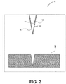
- FIG. 2 illustrates a cross-sectional view of a portion of a debris removal device 10.
- the device 10 includes a nanometer-scaled tip 12 positioned adjacent to a patch or reservoir 14 of low surface energy material.
- the low surface energy material in the reservoir may be solid, liquid, semi-liquid or semi-solid.
- a coating 16 Formed on the tip 12 is a coating 16.
- tip 12 may be pre-coated or otherwise surface treated to modify the surface energy of the tip 12 (e.g., to modify the capillary, wetting, and/or surface tension effects).
- the coating 16 allows the tip 12 to remain sharper for a longer period of time than an uncoated tip.
- a PTFE-coated diamond tip can have a longer operating life than an uncoated diamond tip.
- the coating 16 may include the same low surface energy material found in the patch or reservoir of low energy material 14. Also the tip 12 may be in direct contact with the patch or reservoir of low energy material 14 and the coating 16 may be formed (or replenished) on the surface of tip 12 by rubbing or contacting the tip 12 against the patch or reservoir of low energy material 14. Furthermore, rubbing the tip 12 against the patch or reservoir of low energy material and/or scratching the pad 14 may enhance surface diffusion of the low surface energy material over the surface of tip 12.
- the coating 16 and the patch or reservoir of low energy material 14 may both be made from, or at least may include, chlorinated and fluorinated carbon-containing molecules such as Polytetrafluoroethylene (PTFE) or other similar materials such as Fluorinated ethylene propylene (FEP).
- PTFE Polytetrafluoroethylene
- FEP Fluorinated ethylene propylene
- An intermediate layer 15 of metallic material, oxide, metal oxide, or some other high surface energy material may be disposed between the surface of tip 12 and the low-surface energy material coating 16.
- Some representative examples of the intermediate layer may include, but is not limited to, cesium (Cs), iridium (Ir), and their oxides (as well as chlorides, fluorides, etc.).
- These two exemplary elemental metals are relatively soft metals with low and high surface energies respectively, and thus they represent the optimization of a surface energy gradient optimal for a given contaminate, substrate, and surrounding environment.
- the surface of tip 12 may be roughened or doped.
- the high surface energy material or tip treatment typically acts to bind the low-surface energy material coating 16 to the tip 12 more strongly. Since the shape of the tip also influences localized surface energy density variations (i.e., nanoscale sharpness will greatly increase surface energy density right at the apex), the shape of the tip may also be modified to provide increased selective adhesion of particles to the tip.
- Roughening a tip surface 13 of the tip 12 may also provide greater adhesion due to the increase in surface area of contact with the particle and the number of potential binding sites (dA).
- the tip surface 13 may also be treated (possibly by chemical or plasma processes) so that the tip surface 13 contains highly unstable and chemically active dangling bonds that can react with a particle or some intermediary coating to increase adhesion.
- the tip surface 13 may also be coated with a high surface area material like high density carbon (HDC) or diamond like carbon (DLC) to increase the surface area of the tip 12 interacting with a particle.
- HDC high density carbon
- DLC diamond like carbon
- a high-surface energy pre-treatment is used without a low-surface energy coating 16.
- the particles 20 discussed below may be embedded in some other soft targets (e.g., Au, Al) using similar methods to those discussed herein, or the tip 12 may be a consumable.
- other physical and/or environmental parameters may be modified (e.g., temperature, pressure, chemistry, humidity) to enhance tip treatment and/or particle pick-up/drop-off as will be appreciated by one skilled in the art in view of the present disclosure.
- the patch or reservoir of low energy material 14 is substantially flat and is attached to a stage that supports the substrate 18. Also the patch or reservoir of low energy material 14 is removable from the stage and may easily be replaced or easily refillable. For example, the patch or reservoir of low energy material 14 may be affixed to the AFM with an easily releasable clamp or magnetic mount (not illustrated).
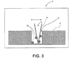
- FIG. 3 illustrates a cross-sectional view of another portion of the debris removal device 10 illustrated in FIG. 2 .
- a substrate 18 that may typically be positioned adjacent to the patch or reservoir of low energy material 14 illustrated in FIG. 2 .
- a plurality of particles 20 that may present in a trench 22 that is formed on the surface of the substrate 18.
- the particles 20 are typically attached to the surfaces of the trench 22 via Van der Waals short-range forces.
- the tip 12 may be moved and positioned adjacent to the substrate 18 to physically attach the particles 20 to the tip 12.
- the tip 12 as illustrated in FIGS. 2 and 3 may be a high aspect ratio tip.
- the particles 20 may be attached to or found on other structures to be cleaned.
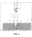
- FIG. 4 illustrates a cross-sectional view of the portion of the debris removal device 10 illustrated in FIG. 2 , wherein the particles 20 may be transferred from the tip 12 and may be imbedded in the patch or reservoir of low energy material 14 by extending the tip 12 into or against a surface of the patch or reservoir of low energy material 14. Subsequently, as shown in the cross-sectional view of FIG. 5 , the tip 12 may be retracted such that the tip 12 is no longer in contact with the patch or reservoir of low energy material 14. As the tip 12 is retracted or withdrawn from the patch or reservoir of low energy material 14, the particles 20 previously on the tip 12 remain with the patch or reservoir of low energy material 14.
- the device 10 illustrated in FIGS. 2-5 may be utilized to implement a method of debris removal. It should also be noted that, although only one tip 12 is discussed and shown in the figures, a plurality of tips may be used simultaneously to remove particles from multiple structures at the same time. Additionally, a plurality of tips could be used in the methods discussed herein in parallel and at the same time.
- the debris method mentioned above may include positioning the tip 12 adjacent to one or more of the particles 20 (i.e., the pieces of debris) illustrated as being on the substrate 18 in FIG. 3 .
- the method may further include physically adhering (as opposed to electrostatically adhering) the particles 20 to the tip 12 as also illustrated in FIG. 3 as well as some possible repetitive motion of the tip 12 when in contact with the particle(s) 20 and surrounding surfaces.
- the method may include removing the particles 20 from the substrate 18 by moving and/or withdrawing the tip 12 away from the substrate 18, and moving the tip 12 with the particles 20 to the patch or reservoir of low energy material 14, as illustrated in FIG. 4 .
- the method may include forming the coating 16 on at least a portion of the tip 12.
- the coating 16 may comprise a coating material that has a lower surface energy than a surface energy of the substrate 18. Additionally or alternatively, the coating 16 may comprise a coating material that has higher surface area than the surface area of the particle 20 that is in contact with the substrate 18.
- some aspects of the method may further include moving the tip 12 to at least a second location of the substrate 18 such that the tip 12 is adjacent to other pieces of particles or debris (not illustrated) such that the other pieces of particles or debris are physically attached to the tip 12
- the other pieces of particles debris may then be removed from the substrate 18 by moving the tip 12 away from the substrate 18 in a manner analogous to what is shown in FIG. 4 .
- some methods may include a step of depositing the piece of debris in a piece of material positioned away from the substrate (e.g., the above-discussed patch or reservoir of low energy material 14).
- the method may include replenishing the coating 16 by plunging the tip 12 in the patch or reservoir of low energy material 14.
- Low surface energy material from the patch or reservoir of low energy material may coat any holes or gaps that may have developed in the coating 16 of the tip 12 over time. This replenishing may involve one or more of moving the tip 12 laterally within the patch or reservoir of low energy material 14 after plunging the tip 12 into the patch or reservoir of low energy material 14, rubbing a surface of the tip 12, or altering a physical parameter (e.g., temperature) of the tip 12 and/or the patch or reservoir of low energy material 14.
- a physical parameter e.g., temperature
- certain methods may include exposing a small area around a defect or particle to a low surface energy material before a repair in order to reduce the likelihood that the removed material will lump together and strongly adhere again to the substrate after the repair is completed.
- a defect/particle and an approximately 1-2 micron area around the defect may be pre-coated with PTFE or FEP according to certain aspects of the present disclosure.
- a tip 12 coated or constructed from a low surface energy material e.g., a PTFE or FEP tip
- a portion or an entirety of the tip 12 may comprise a low energy material such as, but not limited to, chlorinated and fluorinated carbon-containing molecules.
- a low energy material such as, but not limited to, chlorinated and fluorinated carbon-containing molecules.
- examples of such materials may include PTFE or FEP.
- other materials such as metals and their compounds may be used.
- Some representative examples include Cs, Ir, and their oxides (as well as chlorides, fluorides, etc.). These two exemplary elemental metals are relatively soft metals with low and high surface energies respectively, and thus they represent the optimization of a surface energy gradient optimal for a given contaminate, substrate, and surrounding environment. Additionally or alternatively, other carbon based compounds may be used.
- Some representative examples include HDC or DLC.
- the method includes using the patch or reservoir of low energy material 14 to push the particles away from an apex of the tip 12 and toward an AFM cantilever arm (not illustrated) that is supporting the tip 12, above the apex. Such pushing up of the particles 20 may free up space near the apex of the tip 12 physically adhere more particles 20.
- the tip 12 is used to remove nanomachining debris from high aspect ratio structures such as, for example, the trench 22 of the substrate 18, by alternately, dipping, inserting, and/or indenting the tip 12 into a pallet of soft material which may be found in the patch or reservoir of low energy material 14.
- the soft material of the patch or reservoir of low energy material 14 may have a doughy or malleable consistency. This soft material may generally have a greater adherence to the tip 12 and/or debris material (e.g., in the particles 20) than to itself.
- the soft material may also be selected to have polar properties to electrostatically attract the nanomachining debris particles 20 to the tip 12.
- the patch or reservoir of low energy material 14 may comprise a mobile surfactant.
- the tip 12 may include one or more dielectric surfaces (i.e., electrically insulated surfaces). These surfaces may be rubbed on a similarly dielectric surface in certain environmental conditions (e.g., low humidity) to facilitate particle pick-up due to electrostatic surface charging. Also, the coating 16 may attract particles by some other short-range mechanism, which may include, but is not limited to, hydrogen bonding, chemical reaction, enhanced surface diffusion.
- any tip that is strong and stiff enough to penetrate (i.e., indent) the soft pallet material of the patch or reservoir of low energy material 14 may be used.
- very high aspect tip geometries greater than 1:1 are within the scope of the present disclosure.
- high aspect ratio tips that are strong and flexible are generally selected over tips that are weaker and/or less flexible.
- the tip can be rubbed into the sides and corners of the repair trench 22 of the substrate 18 without damaging or altering the trench 22 or the substrate 18.
- a rough macro-scale analogy of this operation is a stiff bristle being moved inside a deep inner diameter.
- the tip 12 may comprise a plurality of rigid or stiff nanofibrils bristles, as will be described in greater detail below.
- each bristle of the plurality of rigid or stiff nanofibrils bristles 30 may extended linearly from the tip 12.
- the plurality of rigid or stiff nanofibrils bristles 30 may be formed with carbon nanontubes, metal whiskers, etc.
- the tip 12 may additionally or alternatively comprise a plurality of flexible or wrap nanofibrils , as will be described in greater detail below.
- the plurality of flexible or wrap nanofibrils may be formed on the tip 12 using polymer materials, for example. Other materials and structures are of course contemplated.
- the detection of whether or not one or more particles have been picked up may be performed by employing a noncontact AFM scan of the region of interest (ROI) to detect particles.
- the tip 12 may then be retracted from the substrate 18 without rescanning until after treatment at the target.
- overall mass of debris material picked up by the tip 12 may also be monitored by relative shifts in the tip's resonant frequency.
- other dynamics may be used for the same function.
- the tip 12 may also be vectored into the patch or reservoir of low energy material 14 to remove the particles 20. As such, if the tip inadvertently picks up a particle 20, the particle 20 can be removed by doing another repair. Particularly when a different material is used for depositing the particles 20 by vectoring, then a soft metal such as a gold foil may be used.
- a ultra-violet (UV)-light-curable material may be used to coat the tip 12 and to form the coating 16.
- UV ultra-violet
- the material picks up particles 20 from the substrate 18.
- the tip 12 may be exposed to a UV source where the material's properties would be changed to make the particles 20 less adherent to the tip 12 and more adherent to the material in the patch or reservoir of low energy material 14, where the particles 20 may subsequently be removed from the tip 12 and deposited with the patch or reservoir of low energy material 14.
- Other nonreversible process which further enhances, or enables, the selectivity of particle pick up and removal are of course contemplated.
- Certain aspects of the present disclosure provide a variety of advantages. For example, certain aspects of the present disclosure allow for active removal of debris from high aspect trench structures using very high aspect AFM tip geometries (greater than 1:1). Also, certain aspects of the present disclosure may be implemented relatively easily by attaching a low surface energy or soft material pallet to an AFM, along with using a very high aspect tip and making relatively minor adjustments to the software repair sequences currently used by AFM operators. In addition, a novel nanomachining tool may be implemented that could be used (like nano-tweezers) to selectively remove particles from the surface of a mask which could not be cleaned by any other method. This may be combined with a more traditional repair where the debris would first be dislodged from the surface with an uncoated tip, then picked up with a coated tip.
- a low surface energy material is used in the local clean methods discussed above, other possible variations are also within the scope of the present disclosure. Typically, these variations create a surface energy gradient (i.e., a Gibbs free energy gradient) that attracts the particle 20 to the tip 12 and may be subsequently reversed by some other treatment to release the particles 20 from the tip 12.
- a surface energy gradient i.e., a Gibbs free energy gradient
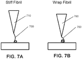
- One aspect not part of the present invention involves the attachment of at least one nanofibril to the working end of an AFM tip to provide enhanced capability in high aspect structures while also allowing for less mechanically aggressive process to the underlying substrate.
- These fibrils can be, according to their mechanical properties and application towards nanoparticle cleaning, classified under two different labels, "stiff' fibrils, and "wrap" fibrils.
- FIGS. 7A and 7B illustrate differences between these 2 types of fibrils, the stiff fibril 700 attached to a tip 710 and the wrap fibril 750 attached to a tip 760.
- the stiff fibril 700 relies more on the mechanical action, and mechanical strength, of the fibril itself to dislodge the nanoparticle. Thus, it also relies on the shear and bending strength and moduli of elasticity to accomplish the dislodgement successfully without breaking. This means there are very few materials which could exceed, or even meet, the strength and stiffness (typically referred to as its hardness) of single crystal diamond. Among these are carbon nanotubes and graphene, since both use the carbon-carbon sp3 hybrid orbital interatomic bonds (one of the strongest known) that are also found in diamond.
- contemplated materials include certain phases of boron-containing chemistries which possess properties that could possibly exceed the mechanical strength and stiffness of diamond so these materials could also be used.
- many materials including diamond can become intrinsically stronger and stiffer as their dimensionality is reduced (with stiffness decreasing as the structure approaches atomic scales and its shape is determined by thermal diffusive behaviors). This is a material phenomenon that was first observed in nanocrystalline metals but has also been confirmed in molecular simulation and some experiment to also occur with single crystal nanopillars.
- One leading hypothesis for this behavior leads into the defect diffusion mechanism of plastic deformation. At larger scales, these crystal defects (vacancies, dislocations, etc.) diffuse and interact in bulk-dominated kinetics.
- FIGS. 8A to 8C illustrate an exemplary process of dislodging and removing a nanoparticle from a target substrate using a single stiff fibril 800 attached at or near the apex of an AFM tip 810.
- the tip 810 approaches the surface and scans using the same principles as an AFM scan without the stiff fibril. It will be appreciated by one skilled in the art that different operational parameters may be applied in view of the single stiff fibril 800 attached to the apex of the tip 810. Once the particle is located, the tip 810 is moved towards a surface 830 and the stiff fibril 800 is elastically deformed, as generally shown in FIG. 8B .
- the deformation of the stiff fibril 800 may be compressive, shear, bending, tensile or a combination thereof and can also be used to mechanically dislodge the nanoparticle 820 from the surface 830. Once the nanoparticle 820 is dislodged, the surface energy and area differences between the stiff fibril 800, substrate 840 and nanoparticle 820 surfaces govern whether the nanoparticle 820 adheres to the stiff fibril 800 when it is subsequently extracted from the substrate surface 830.
- stiff fibril nanoparticle clean process is when two or more stiff fibrils are strongly attached to the tip surface at a distance less than the nanoparticle diameter (but not less than the elastic deformation limit for the stiff fibrils as determined by their shear and bending moduli and length to width ratio), as illustrated in FIGS. 9A to 9C .
- the sequence is very similar to the single stiff fibril as discussed above with reference to FIGS. 8A to 8C .
- the multi-fibril tip 910 may have more potential surface area for the particle 920 to adhere (i.e., wet) to. As the tip 910 is retracted from the substrate, as generally shown in FIG. 9C , another difference emerges if the length and spacing of the fibrils are within the correct range.
- the nanoparticle 920 with this setup has the possibility of becoming mechanically trapped within the spaces between the stiff nanofibrils 900a, 900b, which may result in greater adhesion to the multi-fibril 900a, 900b and a greater probably of extracting the nanoparticle 920 from the substrate surface 930.
- the tip 910 may be re-approached to a surface and the stiff fibrils 900a, 900b again stressed to relax their mechanical entrapment of the nanoparticle 920 thus increasing the probability the nanoparticle 920 will be deposited at the desired surface location.
- the length and spacing of the fibrils 900a, 900b are within the correct range, on the first order model, these ranges include a fibril spacing less than the minimum width of the nanoparticle 920 (assuming a strong nanoparticle that will not crumble), but large enough that the fibrils 900a, 900b will not be bent beyond their shear and bending strength limit (also determined by the relative length of the fibrils and assuming the adhesion strength of the fibril attachment is not less than this limit), as will be appreciated by those skilled in the art in view of the present disclosure.
- the two or more stiff fibrils may have different and unequal lengths.
- a stiff fibril is (as opposed to a wrap fibril), one must be able to define the anisotropic spring constants (related to the effective shear and bending moduli) for a specific material and nano-structure. Since this is very difficult to do in practice, it is assumed for our purposes here that these properties are roughly proportional to the tensile (a.k.a. Young's) elastic modulus and strength.
- the tensile modulus is a possible measure of the stiffness of a material within the stress range where it exhibits elastic (i.e., spring-like) mechanical properties. It is given as the stress divided by the strain, thus yielding units the same as stress (since stain is defined as deformation ratio of final versus initial dimension).
- tensile strength is also important since the fibril must be able to apply sufficient force to dislodge a nanoparticle without breaking-off itself and creating an additional contamination to the substrate surface.
- Strength is also given in units of stress (Pascals).
- the intrinsic tensile modulus is on the order of 1.22 terra-Pascals (TPa) with a tensile strength ranging from 8.7 to 16.5 giga-Pascals (GPa) and provides here our general reference measure for stiffness and strength (approaching within the value for tungsten of 0.5 TPa for tensile elastic modulus, or exceeding these values).
- a wrap fibril in contrast to a stiff fibril, will have much lower spring constants (specified here as elastic tensile moduli) with sufficiently high (comparable) tensile strength.
- elastic tensile moduli the spring constants
- the tensile strength is directly related to its performance since a tensile force is applied to both dislodge and extract the nanoparticle from the substrate surface.
- most mechanical properties quoted in the literature are for the bulk material which should, in principle, be almost completely unrelated to the tensile properties for mono-molecular fibrils (or nano-scale fibrils approaching mono-molecular scales).
- PTFE is typically quoted to have very low tensile elastic modulus and strength in the bulk material (0.5 GPa and maybe ⁇ 20 MPa respectively), but since the molecule's backbone is comprised of carbon-carbon sp-hybrid orbital chemical bonds, its mono-molecular tensile strength should be more comparable to diamond than many other materials, C-nanotubes, and graphene (all of which contain the same kind of chemical bonds). Since the bulk material mechanical properties is more related to the action of single-molecule strands interacting with their neighbors, it should be more comparable to both the cohesive and mono-molecular bending and shear moduli.
- FIGS. 10A to 10C show a nanoparticle cleaning sequence using a wrap (flexible) nanofibril 1000 attached to an AFM tip 1010 near or at the apex. Since there is no compression stress required to deform the wrap-type fibril 1000, the tip 1010 is brought into close proximity to the surface 1030 in order to bring the fibril 1000 into close enough proximity to the nanoparticle surface for short range surface energy forces to allow for the fibril 1000 to adhere to it.
- the relative surface energies of the fibril 1000, nanoparticle 1020, and substrate surfaces 1030 are targeted so that the fibril would preferentially adhere to the nanoparticle surface, once the fibril 1000 is brought into contact with enough slack given the fibril length, only time and applied agitation energies (possibly mechanical and/or thermal) are required to allow the fibril 1000 to wrap around the particle 1020. It is possible that mechanical energies (whether by the tip 1010 with the fibrils 1000 attached, or another tip in a prior processing pass) from a more rigid tip could be applied to initially dislodge the particle 120. Once the fibril 1000 is sufficiently wrapped-around the nanoparticle 1020, as generally shown in FIG. 10B , the tip 1010 is then extracted from the substrate surface 1030.
- the nanoparticle 1020 will be extracted from the substrate 1040 with the tip 1010, as generally shown in FIG. 10C .
- RNA/DNA RNA/DNA
- Actin amyloid nanostructures
- Ionomers RNA/DNA
- DNA deoxyribonucleic acid
- AFM tip 1110 is immersed in the aqueous solution, or placed in AFM-contact to a surface, containing the DNA sequences so that the latter bind as designed.
- the tip 1110 may then be functionalized for particle removal from a substrate surface 1130, as shown in FIGS. 11A to 11D . Moving from left to right in the figures, the functionalized tip 1110 may be moved or actuated to approach near (closer than the length of the DNA strands 1100) the particle 1120 and substrate surfaces 1130, as shown in FIG. 11A .
- a higher temperature may be applied (possibly ⁇ 90°C) with an activating chemistry (either helper DNA strands, also available commercially, or some other ionic activator such as a magnesium salt) while the tip 1110 is near the dislodged particle 1120 as shown in FIG. 11B .
- the environment may then cooled (possibly to ⁇ 20°C) allowing the targeted sequences in the strands 1100 to link up as shown in FIG. 11C (the linking strands 1100 are at the opposite free ends of the molecules).
- the tip 1110 may then be extracted from the substrate surface 1130 as shown in FIG. 11D .
- this bonding between the nanoparticle and the tip it is possible to describe this bonding between the nanoparticle and the tip to be mechanical, however if the particle is on the molecular scale, it could also be described as a steric bond. Steric effects may be created by atomic repulsion at close enough proximity. If an atom or molecule is surrounded by atoms in all possible diffusion directions, it will be effectively trapped and unable to chemically of physically interact with any other atoms or molecules in its environment. RNA can similarly be manipulated as will be appreciated by those skilled in the art in view of the present disclosure.
- the next possible wrap nano-fibril candidate is a family of similar globular multifunction proteins that forms filaments in eukaryotic cells, one of which is known as actin. Actin is used inside cells for scaffolding, anchoring, mechanical supports, and binding, which would indicate it is a highly adaptable and sufficiently strong protein filament. It would be applied and used in methods very similar to the DNA-origami related process discussed above. Experiments indicate that this protein can be crystalized to a molecule of dimensions of 6.7 x 4.0 x 3.7 nm.
- Fibrillar nanostructures like this have several advantages including: underwater adhesion, tolerance to environmental deterioration, self-healing from self-polymerization, and large fibril surface areas. As previously discussed, large fibril surface areas enhance adhesion by increasing the contact area in the adhesive plaques of barnacles. Amyloid nanostructures also have possible mechanical advantages such as cohesive strength associated with the generic amyloid intermolecular ⁇ -sheet structure and adhesive strength related to adhesive residues external to the amyloid core. These properties make amyloid structures a basis for a promising new generation of bio-inspired adhesives for a wide range of applications.
- a wrap fibril material is a class of polymers known as ionomers.
- these are long thermoplastic polymer molecules that strongly bind at targeted ionic charged sites along the molecular chain.
- a common example of an ionomer chemistry is poly(ethylene-co-methacrylic acid).
- the ionomer may be functionalized to the surface of a scanning thermal probe. The process for cleaning a nanoparticle would then be very similar to that shown for the DNA-origami process discussed above except that an aqueous environment would not necessarily be required especially when used with the scanning thermal probe.
- An ionomer functionalization coating may also be paired with an ionic surfactant for preferential conjugate bonding within an aqueous (or similar solvent) environment. It should be mentioned that these examples (especially DNA/RNA and actin) are highly biocompatible for removal and manipulation of nano-particulate entities inside living structures such as cells.
- one variation that may be used includes using a high surface energy tip coating.
- Another variation includes pretreating the particles with a low surface energy material to debond the particles and then contacting the particles with a high surface energy tip coating (sometimes on a different tip).
- Still another variation includes making use of a chemical energy gradient that corresponds to a chemical reaction occurring between a tip surface coating and the particle surface to bond the two. This may either be performed until a tip is exhausted or reversed with some other treatment.
- Adhesives or sticky coatings are used in combination with one or more of the above-listed factors. Also, the surface roughness or small scale (e.g., nanometer-scale) texture can be engineered to maximize particle clean process efficiency.
- mechanical bonding may be used, typically when the tip 12 includes fibrils that, analogously to a mop, are capable of mechanically entangling the particles 20.
- the mechanical entanglement is driven by and/or enhanced by surface energy or chemical changes with contact or environment.
- the tip 12 may be coated with molecular tweezers (i.e., molecular clips). These tweezers may comprise noncyclic compounds with open cavities capable of binding guests (e.g., the above-discussed particles 20). The open cavity of the tweezers typically binds guests using non-covalent bonding including hydrogen bonding, metal coordination, hydrophobic forces, van der Waals forces, ⁇ - ⁇ interactions, and/or electrostatic effects. These tweezers are sometimes analogous to macrocyclic molecular receptors except that the two arms that bind the guest molecules are typically only connected at one end.
- the particles 20 may be removed by the tip using diffusion bonding or Casmir effects.
- bristles or fibrils 30 can be attached to the end of the tip 12. Whether strategically or randomly placed, these bristles or fibrils 30 can enhance local clean in several ways. For example, an associated increase in surface area may be used for surface (short range) bonding to the particles.
- Fibrils 30 are engineered to be molecules that selectively (e.g., by either surface or environment) coil around and entangle a particle 20, thus maximizing surface contact. Also, dislodging of the particles 20 occurs according to certain aspects of the present disclosure, typically when stiffbristles 30 are attached to the tip 12. However, fibrils 30 may also entangle a particle 20 and dislodge the particle 20 mechanically by pulling on the particle 20. In contrast, relatively rigid bristles 30 typically allow the tip 12 to extend into hard-to-reach crevices. Then, by impact deformation stress of the bristles 30, by surface-modification of the tip 12 to repel particles 20, or by some combination, the particle 20 is dislodged.
- certain aspects of the present disclosure mechanically bond the particles 20 to the tip 12.
- fibrils are on the tip 12, entanglement of one or more of either the whole or frayed fibrils may occur.
- the particle 20 may be wedged between (elastically) stressed bristles.
- Methods of debris removal include changing the environment to facilitate local clean.
- gas or liquid media may be introduced or the chemistry and/or physical properties (e.g., pressure, temperature, and humidity) may be changed.
- certain aspects of the present disclosure include an image recognition system that identifies debris to be removed.
- an automatic debris-removal device is also within the scope of the present disclosure.
- a relatively soft cleaning tip is used to avoid unwanted damage to inside contours, walls, and/or bottom of a complex shape.
- a stronger force is used to bring the relatively soft tip into much stronger contact with the surface while also increasing the scan speed.
- a tip exposed to and/or coated with a low surface energy material may be used for other purposes besides removing debris (cleaning) of nanometer level structures.
- such tips can also be used, according to certain aspects of the present disclosure, to periodically lubricate micron level or smaller devices (like MEMS/NEMS) to contain chemical reactions.
- This method may be performed in a variety of environments according to the requirements of the application and to further enhance differential adhesion of the particle from the substrate surface to the patch or reservoir of low energy material.
- environments may include, but are not limited to, vacuum, shield gasses of various composition and pressure, and fluids of variable composition (including fluids with varying ionic strengths and/or pHs).
- the deformation of the tip material may also provide a mechanism of mechanical entrapment of the debris especially if it is roughened (or covered in nano-bristles) and/or if it has a high microstructural defect (i.e., void) density at the surface.
- the final factor that will be discussed will be chemical potential energy. It is possible to modify the chemical state of the tip and/or soft patch surfaces to create preferential chemical reactions to bond the debris material to the tip. These chemical bonds may be covalent or ionic in nature (with the sp3-hybid orbital covalent bond being the strongest).
- the debris may be coated with one component of a targeted lock-and-key chemically bonding pair of chemistries.
- the tip (or another tip) may be coated with the other chemical and brought in contact with the debris surface to bond it to the tip.
- One non-limiting example of a lock-and-key pair of chemistries is streptavidin and biotin which is often used in Chemical Force Microscopy (CFM) experiments.
- Another example using an ionic bond would be two surfactant polar molecular chemistries where the exposed polar ends of the molecules on the debris and tip surface are of opposite charge.
- CFM Chemical Force Microscopy
- Chemical changes to the tip surface would also allow for targeted changes to its surface energy as well as phase changes (in particular from fluid to solid) that may surround (to maximize surface area dA) and mechanically entrap the debris at the tip surface in order to bond it.
- These chemical changes may be catalyzed by external energy sources such as heat (temperature), ultraviolet light, and charged particle beams.
Landscapes
- General Physics & Mathematics (AREA)
- Physics & Mathematics (AREA)
- Engineering & Computer Science (AREA)
- Nuclear Medicine, Radiotherapy & Molecular Imaging (AREA)
- Radiology & Medical Imaging (AREA)
- Health & Medical Sciences (AREA)
- General Health & Medical Sciences (AREA)
- Nanotechnology (AREA)
- Chemical & Material Sciences (AREA)
- Condensed Matter Physics & Semiconductors (AREA)
- Manufacturing & Machinery (AREA)
- Computer Hardware Design (AREA)
- Microelectronics & Electronic Packaging (AREA)
- Power Engineering (AREA)
- Cleaning In General (AREA)
- Preparing Plates And Mask In Photomechanical Process (AREA)
Claims (4)
- Ein Verfahren zum Entfernen eines Fremdkörpers (2, 20) von einer Oberfläche eines Substrats (3), das umfasst:Positionieren einer Spitze (12) neben dem Fremdkörper (2, 20) auf dem Substrat (3);Katalysieren einer Phasenänderung eines Fluids zu einem Feststoff, um den Fremdkörper (2, 20) an einer Oberfläche der Spitze (12) einzufangen, undEntfernen des Fremdkörpers (2, 20) von der Oberfläche des Substrats (3) durch Bewegen der Spitze (12) weg von dem Substrat (3);dadurch gekennzeichnet, dass der Schritt des Katalysierens mittels einer externen Energiequelle, die ein geladener Teilchenstrahl ist, durchgeführt wird; undwobei das Substrat (3) eine Fotomaske für die Extremultraviolettlithografie ist.
- Das Verfahren gemäß Anspruch 1, das zusätzlich den Schritt des Entfernens des Fremdkörpers (2, 20) von der Spitze umfasst.
- Eine Vorrichtung zum Entfernen eines Fremdkörpers (2, 20) von einer Oberfläche eines Substrats (3), die umfasst:Mittel zum Positionieren einer Spitze (12) neben dem Fremdkörper (2, 20) auf dem Substrat (3);Mittel zum Katalysieren einer Phasenänderung eines Fluids zu einem Feststoff, um den Fremdkörper (2, 20) an einer Oberfläche der Spitze (12) einzufangen, undMittel zum Entfernen des Fremdkörpers (2, 20) von der Oberfläche des Substrats (3) durch Bewegen der Spitze (12) weg von dem Substrat (3);dadurch gekennzeichnet, dass die Mittel zum Katalysieren dafür ausgelegt sind, eine externe Energiequelle, die ein geladener Teilchenstrahl ist, bereitzustellen; unddas Substrat (3) eine Fotomaske für die Extremultraviolettlithographie ist.
- Die Vorrichtung gemäß Anspruch 3, die zusätzlich Mittel zum Entfernen des Fremdkörpers (2, 20) von der Spitze (12) umfasst.
Priority Applications (1)
| Application Number | Priority Date | Filing Date | Title |
|---|---|---|---|
| PL20189018T PL3748431T3 (pl) | 2016-01-29 | 2017-01-26 | Usuwanie zanieczyszczeń ze struktur konstrukcji o wysokim współczynniku |
Applications Claiming Priority (3)
| Application Number | Priority Date | Filing Date | Title |
|---|---|---|---|
| US15/011,411 US10618080B2 (en) | 2007-09-17 | 2016-01-29 | Debris removal from high aspect structures |
| PCT/US2017/015062 WO2017132331A1 (en) | 2016-01-29 | 2017-01-26 | Debris removal from high aspect structures |
| EP17744875.0A EP3408707A4 (de) | 2016-01-29 | 2017-01-26 | Rückstandsentfernung aus strukturen mit hohem aspektverhältnis |
Related Parent Applications (1)
| Application Number | Title | Priority Date | Filing Date |
|---|---|---|---|
| EP17744875.0A Division EP3408707A4 (de) | 2016-01-29 | 2017-01-26 | Rückstandsentfernung aus strukturen mit hohem aspektverhältnis |
Publications (2)
| Publication Number | Publication Date |
|---|---|
| EP3748431A1 EP3748431A1 (de) | 2020-12-09 |
| EP3748431B1 true EP3748431B1 (de) | 2021-09-08 |
Family
ID=59398723
Family Applications (2)
| Application Number | Title | Priority Date | Filing Date |
|---|---|---|---|
| EP20189018.3A Active EP3748431B1 (de) | 2016-01-29 | 2017-01-26 | Rückstandsentfernung aus strukturen mit hohem aspektverhältnis |
| EP17744875.0A Pending EP3408707A4 (de) | 2016-01-29 | 2017-01-26 | Rückstandsentfernung aus strukturen mit hohem aspektverhältnis |
Family Applications After (1)
| Application Number | Title | Priority Date | Filing Date |
|---|---|---|---|
| EP17744875.0A Pending EP3408707A4 (de) | 2016-01-29 | 2017-01-26 | Rückstandsentfernung aus strukturen mit hohem aspektverhältnis |
Country Status (6)
| Country | Link |
|---|---|
| EP (2) | EP3748431B1 (de) |
| JP (1) | JP2019506637A (de) |
| KR (2) | KR102306619B1 (de) |
| DK (1) | DK3748431T3 (de) |
| PL (1) | PL3748431T3 (de) |
| WO (1) | WO2017132331A1 (de) |
Citations (4)
| Publication number | Priority date | Publication date | Assignee | Title |
|---|---|---|---|---|
| JP2005084582A (ja) | 2003-09-11 | 2005-03-31 | Sii Nanotechnology Inc | フォトマスクのパーティクル除去方法 |
| JP2009265176A (ja) | 2008-04-22 | 2009-11-12 | Toshiba Corp | 異物除去方法、異物除去装置および半導体装置の作製方法 |
| US8334084B2 (en) | 2008-06-18 | 2012-12-18 | Rave Llc | Method for fabricating high aspect ratio nanostructures |
| WO2014125494A1 (en) | 2013-02-17 | 2014-08-21 | Carl Zeiss Sms Ltd | Surface defect repair by irradiation |
Family Cites Families (19)
| Publication number | Priority date | Publication date | Assignee | Title |
|---|---|---|---|---|
| US5824470A (en) * | 1995-05-30 | 1998-10-20 | California Institute Of Technology | Method of preparing probes for sensing and manipulating microscopic environments and structures |
| JP2002329700A (ja) * | 2001-04-27 | 2002-11-15 | Sony Corp | 表面処理方法 |
| US6817052B2 (en) * | 2001-11-09 | 2004-11-16 | Formfactor, Inc. | Apparatuses and methods for cleaning test probes |
| AU2003294586A1 (en) * | 2002-12-09 | 2004-06-30 | The University Of North Carolina At Chapel Hill | Methods for assembly and sorting of nanostructure-containing materials and related articles |
| US20050208304A1 (en) * | 2003-02-21 | 2005-09-22 | California Institute Of Technology | Coatings for carbon nanotubes |
| WO2005068137A1 (en) * | 2004-01-05 | 2005-07-28 | Lewis & Clark College | Self-cleaning adhesive structure and methods |
| JP2006351595A (ja) * | 2005-06-13 | 2006-12-28 | Hitachi High-Technologies Corp | 基板処理装置、基板処理方法、及び基板の製造方法 |
| JP2007298858A (ja) * | 2006-05-02 | 2007-11-15 | Hoya Corp | マスクブランク用基板の製造方法、マスクブランクの製造方法、及び露光用マスクの製造方法、並びに、マスクブランク、及び露光用マスク |
| US8499645B2 (en) * | 2007-02-21 | 2013-08-06 | The Board Of Trustees Of The University Of Illinois | Stress micro mechanical test cell, device, system and methods |
| US8287653B2 (en) * | 2007-09-17 | 2012-10-16 | Rave, Llc | Debris removal in high aspect structures |
| KR20090103200A (ko) * | 2008-03-27 | 2009-10-01 | 주식회사 하이닉스반도체 | 포토마스크의 파티클 제거방법 |
| JP2010117412A (ja) * | 2008-11-11 | 2010-05-27 | Shin-Etsu Chemical Co Ltd | フォトマスク関連基板の洗浄方法 |
| US8956463B2 (en) * | 2008-10-08 | 2015-02-17 | Shin-Etsu Chemical Co., Ltd. | Method for cleaning photomask-related substrate, cleaning method, and cleaning fluid supplying apparatus |
| JP5236418B2 (ja) * | 2008-10-08 | 2013-07-17 | 信越化学工業株式会社 | 洗浄方法および洗浄液供給装置 |
| JP2010117403A (ja) * | 2008-11-11 | 2010-05-27 | Shin-Etsu Chemical Co Ltd | フォトマスク関連基板の洗浄方法 |
| JP2010170019A (ja) * | 2009-01-26 | 2010-08-05 | Toshiba Corp | リソグラフィ原版の異物除去方法及びリソグラフィ原版の製造方法 |
| JP2013068786A (ja) * | 2011-09-22 | 2013-04-18 | Toppan Printing Co Ltd | フォトマスクの洗浄方法 |
| US8605281B2 (en) * | 2011-10-13 | 2013-12-10 | Hewlett-Packard Development Company, L.P. | Probe having nano-fingers |
| US20170065069A1 (en) * | 2014-02-27 | 2017-03-09 | Indian Institute Of Technology Kanpur | Nanobrushes and methods of manufacture and use |
-
2017
- 2017-01-26 PL PL20189018T patent/PL3748431T3/pl unknown
- 2017-01-26 EP EP20189018.3A patent/EP3748431B1/de active Active
- 2017-01-26 JP JP2018539846A patent/JP2019506637A/ja active Pending
- 2017-01-26 EP EP17744875.0A patent/EP3408707A4/de active Pending
- 2017-01-26 KR KR1020207022340A patent/KR102306619B1/ko active IP Right Grant
- 2017-01-26 WO PCT/US2017/015062 patent/WO2017132331A1/en active Application Filing
- 2017-01-26 KR KR1020187024622A patent/KR20180107184A/ko not_active Application Discontinuation
- 2017-01-26 DK DK20189018.3T patent/DK3748431T3/da active
Patent Citations (4)
| Publication number | Priority date | Publication date | Assignee | Title |
|---|---|---|---|---|
| JP2005084582A (ja) | 2003-09-11 | 2005-03-31 | Sii Nanotechnology Inc | フォトマスクのパーティクル除去方法 |
| JP2009265176A (ja) | 2008-04-22 | 2009-11-12 | Toshiba Corp | 異物除去方法、異物除去装置および半導体装置の作製方法 |
| US8334084B2 (en) | 2008-06-18 | 2012-12-18 | Rave Llc | Method for fabricating high aspect ratio nanostructures |
| WO2014125494A1 (en) | 2013-02-17 | 2014-08-21 | Carl Zeiss Sms Ltd | Surface defect repair by irradiation |
Non-Patent Citations (4)
| Title |
|---|
| "EUV LITHOGRAPHY / VIVEK BAKSHI", 2009, SPIE, article "Chapter 7", pages: 325 - 381 |
| DENISYUK ANDREY I., KRASAVIN ALEXEY V., KOMISSARENKO FILIPP E., MUKHIN IVAN S.: "Mechanical, Electrostatic, and Electromagnetic Manipulation of Microobjects and Nanoobjects in Electron Microscopes", ADVANCES IN IMAGING AND ELECTRON PHYSICS, vol. 186, 2014, pages 101 - 140, XP055933112 |
| PEI-YANG YAN; MICHAEL LEESON; SANG LEE; GUOJING ZHANG; ERIC GULLIKSON; FARHAD SALMASSI: "Extreme ultraviolet-embedded phase-shift mask", J. MICRO/NANOLITH., vol. 10, no. 3, July 2011 (2011-07-01), pages 1 - 11, XP055016128 |
| ROBINSON TOD, DINSDALE ANDREW, ARCHULETTA MIKE, BOZAK RON, WHITE ROY: "Nanomachining photomask repair of complex patterns", PROC. SPIE 7122, PHOTOMASK TECHNOLOGY, vol. 7122, 17 October 2008 (2008-10-17), pages 1 - 12, XP055933103 |
Also Published As
| Publication number | Publication date |
|---|---|
| JP2023022833A (ja) | 2023-02-15 |
| EP3748431A1 (de) | 2020-12-09 |
| WO2017132331A1 (en) | 2017-08-03 |
| KR20180107184A (ko) | 2018-10-01 |
| JP2019506637A (ja) | 2019-03-07 |
| EP3408707A4 (de) | 2019-11-06 |
| KR102306619B1 (ko) | 2021-10-01 |
| KR20200096673A (ko) | 2020-08-12 |
| PL3748431T3 (pl) | 2022-01-24 |
| EP3408707A1 (de) | 2018-12-05 |
| DK3748431T3 (da) | 2021-12-06 |
Similar Documents
| Publication | Publication Date | Title |
|---|---|---|
| US11964310B2 (en) | Debris removal from high aspect structures | |
| US10618080B2 (en) | Debris removal from high aspect structures | |
| US11391664B2 (en) | Debris removal from high aspect structures | |
| EP3726566B1 (de) | Entfernung von ablagerungen aus einem graben, der auf einer photolithographischen maske gebildet wurde | |
| JP2022050485A (ja) | 高アスペクト構造からのデブリ除去 | |
| KR102433627B1 (ko) | 고종횡비 구조물에서 잔해물 제거 | |
| EP3748431B1 (de) | Rückstandsentfernung aus strukturen mit hohem aspektverhältnis | |
| JP7495087B2 (ja) | 高アスペクト構造からのデブリ除去 | |
| TWI841110B (zh) | 從高深寬比結構移除碎片 |
Legal Events
| Date | Code | Title | Description |
|---|---|---|---|
| PUAI | Public reference made under article 153(3) epc to a published international application that has entered the european phase |
Free format text: ORIGINAL CODE: 0009012 |
|
| STAA | Information on the status of an ep patent application or granted ep patent |
Free format text: STATUS: EXAMINATION IS IN PROGRESS |
|
| 17P | Request for examination filed |
Effective date: 20200731 |
|
| AC | Divisional application: reference to earlier application |
Ref document number: 3408707 Country of ref document: EP Kind code of ref document: P |
|
| AK | Designated contracting states |
Kind code of ref document: A1 Designated state(s): AL AT BE BG CH CY CZ DE DK EE ES FI FR GB GR HR HU IE IS IT LI LT LU LV MC MK MT NL NO PL PT RO RS SE SI SK SM TR |
|
| STAA | Information on the status of an ep patent application or granted ep patent |
Free format text: STATUS: EXAMINATION IS IN PROGRESS |
|
| RBV | Designated contracting states (corrected) |
Designated state(s): AL AT BE BG CH CY CZ DE DK EE ES FI FR GB GR HR HU IE IS IT LI LT LU LV MC MK MT NL NO PL PT RO RS SE SI SK SM TR |
|
| GRAP | Despatch of communication of intention to grant a patent |
Free format text: ORIGINAL CODE: EPIDOSNIGR1 |
|
| STAA | Information on the status of an ep patent application or granted ep patent |
Free format text: STATUS: GRANT OF PATENT IS INTENDED |
|
| INTG | Intention to grant announced |
Effective date: 20210607 |
|
| GRAS | Grant fee paid |
Free format text: ORIGINAL CODE: EPIDOSNIGR3 |
|
| GRAA | (expected) grant |
Free format text: ORIGINAL CODE: 0009210 |
|
| STAA | Information on the status of an ep patent application or granted ep patent |
Free format text: STATUS: THE PATENT HAS BEEN GRANTED |
|
| AC | Divisional application: reference to earlier application |
Ref document number: 3408707 Country of ref document: EP Kind code of ref document: P |
|
| AK | Designated contracting states |
Kind code of ref document: B1 Designated state(s): AL AT BE BG CH CY CZ DE DK EE ES FI FR GB GR HR HU IE IS IT LI LT LU LV MC MK MT NL NO PL PT RO RS SE SI SK SM TR |
|
| REG | Reference to a national code |
Ref country code: GB Ref legal event code: FG4D |
|
| REG | Reference to a national code |
Ref country code: AT Ref legal event code: REF Ref document number: 1429103 Country of ref document: AT Kind code of ref document: T Effective date: 20210915 Ref country code: CH Ref legal event code: EP |
|
| REG | Reference to a national code |
Ref country code: IE Ref legal event code: FG4D |
|
| REG | Reference to a national code |
Ref country code: DE Ref legal event code: R096 Ref document number: 602017045925 Country of ref document: DE |
|
| REG | Reference to a national code |
Ref country code: DK Ref legal event code: T3 Effective date: 20211203 |
|
| REG | Reference to a national code |
Ref country code: NL Ref legal event code: FP |
|
| REG | Reference to a national code |
Ref country code: LT Ref legal event code: MG9D |
|
| PG25 | Lapsed in a contracting state [announced via postgrant information from national office to epo] |
Ref country code: NO Free format text: LAPSE BECAUSE OF FAILURE TO SUBMIT A TRANSLATION OF THE DESCRIPTION OR TO PAY THE FEE WITHIN THE PRESCRIBED TIME-LIMIT Effective date: 20211208 Ref country code: HR Free format text: LAPSE BECAUSE OF FAILURE TO SUBMIT A TRANSLATION OF THE DESCRIPTION OR TO PAY THE FEE WITHIN THE PRESCRIBED TIME-LIMIT Effective date: 20210908 Ref country code: FI Free format text: LAPSE BECAUSE OF FAILURE TO SUBMIT A TRANSLATION OF THE DESCRIPTION OR TO PAY THE FEE WITHIN THE PRESCRIBED TIME-LIMIT Effective date: 20210908 Ref country code: LT Free format text: LAPSE BECAUSE OF FAILURE TO SUBMIT A TRANSLATION OF THE DESCRIPTION OR TO PAY THE FEE WITHIN THE PRESCRIBED TIME-LIMIT Effective date: 20210908 Ref country code: BG Free format text: LAPSE BECAUSE OF FAILURE TO SUBMIT A TRANSLATION OF THE DESCRIPTION OR TO PAY THE FEE WITHIN THE PRESCRIBED TIME-LIMIT Effective date: 20211208 Ref country code: ES Free format text: LAPSE BECAUSE OF FAILURE TO SUBMIT A TRANSLATION OF THE DESCRIPTION OR TO PAY THE FEE WITHIN THE PRESCRIBED TIME-LIMIT Effective date: 20210908 Ref country code: RS Free format text: LAPSE BECAUSE OF FAILURE TO SUBMIT A TRANSLATION OF THE DESCRIPTION OR TO PAY THE FEE WITHIN THE PRESCRIBED TIME-LIMIT Effective date: 20210908 Ref country code: SE Free format text: LAPSE BECAUSE OF FAILURE TO SUBMIT A TRANSLATION OF THE DESCRIPTION OR TO PAY THE FEE WITHIN THE PRESCRIBED TIME-LIMIT Effective date: 20210908 |
|
| PG25 | Lapsed in a contracting state [announced via postgrant information from national office to epo] |
Ref country code: LV Free format text: LAPSE BECAUSE OF FAILURE TO SUBMIT A TRANSLATION OF THE DESCRIPTION OR TO PAY THE FEE WITHIN THE PRESCRIBED TIME-LIMIT Effective date: 20210908 Ref country code: GR Free format text: LAPSE BECAUSE OF FAILURE TO SUBMIT A TRANSLATION OF THE DESCRIPTION OR TO PAY THE FEE WITHIN THE PRESCRIBED TIME-LIMIT Effective date: 20211209 |
|
| PG25 | Lapsed in a contracting state [announced via postgrant information from national office to epo] |
Ref country code: IS Free format text: LAPSE BECAUSE OF FAILURE TO SUBMIT A TRANSLATION OF THE DESCRIPTION OR TO PAY THE FEE WITHIN THE PRESCRIBED TIME-LIMIT Effective date: 20220108 Ref country code: SM Free format text: LAPSE BECAUSE OF FAILURE TO SUBMIT A TRANSLATION OF THE DESCRIPTION OR TO PAY THE FEE WITHIN THE PRESCRIBED TIME-LIMIT Effective date: 20210908 Ref country code: SK Free format text: LAPSE BECAUSE OF FAILURE TO SUBMIT A TRANSLATION OF THE DESCRIPTION OR TO PAY THE FEE WITHIN THE PRESCRIBED TIME-LIMIT Effective date: 20210908 Ref country code: RO Free format text: LAPSE BECAUSE OF FAILURE TO SUBMIT A TRANSLATION OF THE DESCRIPTION OR TO PAY THE FEE WITHIN THE PRESCRIBED TIME-LIMIT Effective date: 20210908 Ref country code: PT Free format text: LAPSE BECAUSE OF FAILURE TO SUBMIT A TRANSLATION OF THE DESCRIPTION OR TO PAY THE FEE WITHIN THE PRESCRIBED TIME-LIMIT Effective date: 20220110 Ref country code: EE Free format text: LAPSE BECAUSE OF FAILURE TO SUBMIT A TRANSLATION OF THE DESCRIPTION OR TO PAY THE FEE WITHIN THE PRESCRIBED TIME-LIMIT Effective date: 20210908 Ref country code: AL Free format text: LAPSE BECAUSE OF FAILURE TO SUBMIT A TRANSLATION OF THE DESCRIPTION OR TO PAY THE FEE WITHIN THE PRESCRIBED TIME-LIMIT Effective date: 20210908 |
|
| REG | Reference to a national code |
Ref country code: DE Ref legal event code: R026 Ref document number: 602017045925 Country of ref document: DE |
|
| PLBI | Opposition filed |
Free format text: ORIGINAL CODE: 0009260 |
|
| PLAB | Opposition data, opponent's data or that of the opponent's representative modified |
Free format text: ORIGINAL CODE: 0009299OPPO |
|
| PLAX | Notice of opposition and request to file observation + time limit sent |
Free format text: ORIGINAL CODE: EPIDOSNOBS2 |
|
| 26 | Opposition filed |
Opponent name: CARL ZEISS SMT GMBH Effective date: 20220608 |
|
| R26 | Opposition filed (corrected) |
Opponent name: CARL ZEISS SMT GMBH Effective date: 20220608 |
|
| PG25 | Lapsed in a contracting state [announced via postgrant information from national office to epo] |
Ref country code: MC Free format text: LAPSE BECAUSE OF FAILURE TO SUBMIT A TRANSLATION OF THE DESCRIPTION OR TO PAY THE FEE WITHIN THE PRESCRIBED TIME-LIMIT Effective date: 20210908 |
|
| PLBB | Reply of patent proprietor to notice(s) of opposition received |
Free format text: ORIGINAL CODE: EPIDOSNOBS3 |
|
| REG | Reference to a national code |
Ref country code: AT Ref legal event code: UEP Ref document number: 1429103 Country of ref document: AT Kind code of ref document: T Effective date: 20210908 |
|
| PGFP | Annual fee paid to national office [announced via postgrant information from national office to epo] |
Ref country code: FR Payment date: 20230125 Year of fee payment: 7 Ref country code: DK Payment date: 20230127 Year of fee payment: 7 |
|
| PGFP | Annual fee paid to national office [announced via postgrant information from national office to epo] |
Ref country code: PL Payment date: 20230202 Year of fee payment: 7 Ref country code: IT Payment date: 20230221 Year of fee payment: 7 Ref country code: BE Payment date: 20230127 Year of fee payment: 7 |
|
| P01 | Opt-out of the competence of the unified patent court (upc) registered |
Effective date: 20230519 |
|
| RDAF | Communication despatched that patent is revoked |
Free format text: ORIGINAL CODE: EPIDOSNREV1 |
|
| APAH | Appeal reference modified |
Free format text: ORIGINAL CODE: EPIDOSCREFNO |
|
| APBM | Appeal reference recorded |
Free format text: ORIGINAL CODE: EPIDOSNREFNO |
|
| APBP | Date of receipt of notice of appeal recorded |
Free format text: ORIGINAL CODE: EPIDOSNNOA2O |
|
| PGFP | Annual fee paid to national office [announced via postgrant information from national office to epo] |
Ref country code: NL Payment date: 20240126 Year of fee payment: 8 |
|
| PGFP | Annual fee paid to national office [announced via postgrant information from national office to epo] |
Ref country code: LU Payment date: 20240129 Year of fee payment: 8 |
|
| APBQ | Date of receipt of statement of grounds of appeal recorded |
Free format text: ORIGINAL CODE: EPIDOSNNOA3O |
|
| PGFP | Annual fee paid to national office [announced via postgrant information from national office to epo] |
Ref country code: IE Payment date: 20240129 Year of fee payment: 8 |
|
| PGFP | Annual fee paid to national office [announced via postgrant information from national office to epo] |
Ref country code: AT Payment date: 20240104 Year of fee payment: 8 |
|
| PG25 | Lapsed in a contracting state [announced via postgrant information from national office to epo] |
Ref country code: MK Free format text: LAPSE BECAUSE OF FAILURE TO SUBMIT A TRANSLATION OF THE DESCRIPTION OR TO PAY THE FEE WITHIN THE PRESCRIBED TIME-LIMIT Effective date: 20210908 Ref country code: CY Free format text: LAPSE BECAUSE OF FAILURE TO SUBMIT A TRANSLATION OF THE DESCRIPTION OR TO PAY THE FEE WITHIN THE PRESCRIBED TIME-LIMIT Effective date: 20210908 |
|
| PGFP | Annual fee paid to national office [announced via postgrant information from national office to epo] |
Ref country code: DE Payment date: 20240129 Year of fee payment: 8 Ref country code: CZ Payment date: 20240109 Year of fee payment: 8 Ref country code: GB Payment date: 20240129 Year of fee payment: 8 Ref country code: CH Payment date: 20240201 Year of fee payment: 8 |