EP3739635B1 - Vorrichtung mit einer aktiven komponente und zugehörige elektroden sowie verfahren zur herstellung solch einer vorrichtung - Google Patents
Vorrichtung mit einer aktiven komponente und zugehörige elektroden sowie verfahren zur herstellung solch einer vorrichtung Download PDFInfo
- Publication number
- EP3739635B1 EP3739635B1 EP20177053.4A EP20177053A EP3739635B1 EP 3739635 B1 EP3739635 B1 EP 3739635B1 EP 20177053 A EP20177053 A EP 20177053A EP 3739635 B1 EP3739635 B1 EP 3739635B1
- Authority
- EP
- European Patent Office
- Prior art keywords
- vertical structure
- semi
- highly
- optoelectronic component
- active optoelectronic
- Prior art date
- Legal status (The legal status is an assumption and is not a legal conclusion. Google has not performed a legal analysis and makes no representation as to the accuracy of the status listed.)
- Active
Links
Images



Classifications
-
- H—ELECTRICITY
- H10—SEMICONDUCTOR DEVICES; ELECTRIC SOLID-STATE DEVICES NOT OTHERWISE PROVIDED FOR
- H10D—INORGANIC ELECTRIC SEMICONDUCTOR DEVICES
- H10D8/00—Diodes
- H10D8/01—Manufacture or treatment
-
- H—ELECTRICITY
- H01—ELECTRIC ELEMENTS
- H01S—DEVICES USING THE PROCESS OF LIGHT AMPLIFICATION BY STIMULATED EMISSION OF RADIATION [LASER] TO AMPLIFY OR GENERATE LIGHT; DEVICES USING STIMULATED EMISSION OF ELECTROMAGNETIC RADIATION IN WAVE RANGES OTHER THAN OPTICAL
- H01S5/00—Semiconductor lasers
- H01S5/02—Structural details or components not essential to laser action
- H01S5/0206—Substrates, e.g. growth, shape, material, removal or bonding
- H01S5/0208—Semi-insulating substrates
-
- H—ELECTRICITY
- H01—ELECTRIC ELEMENTS
- H01S—DEVICES USING THE PROCESS OF LIGHT AMPLIFICATION BY STIMULATED EMISSION OF RADIATION [LASER] TO AMPLIFY OR GENERATE LIGHT; DEVICES USING STIMULATED EMISSION OF ELECTROMAGNETIC RADIATION IN WAVE RANGES OTHER THAN OPTICAL
- H01S5/00—Semiconductor lasers
- H01S5/04—Processes or apparatus for excitation, e.g. pumping, e.g. by electron beams
- H01S5/042—Electrical excitation ; Circuits therefor
- H01S5/0425—Electrodes, e.g. characterised by the structure
- H01S5/04256—Electrodes, e.g. characterised by the structure characterised by the configuration
-
- H—ELECTRICITY
- H10—SEMICONDUCTOR DEVICES; ELECTRIC SOLID-STATE DEVICES NOT OTHERWISE PROVIDED FOR
- H10D—INORGANIC ELECTRIC SEMICONDUCTOR DEVICES
- H10D8/00—Diodes
- H10D8/50—PIN diodes
-
- H—ELECTRICITY
- H01—ELECTRIC ELEMENTS
- H01S—DEVICES USING THE PROCESS OF LIGHT AMPLIFICATION BY STIMULATED EMISSION OF RADIATION [LASER] TO AMPLIFY OR GENERATE LIGHT; DEVICES USING STIMULATED EMISSION OF ELECTROMAGNETIC RADIATION IN WAVE RANGES OTHER THAN OPTICAL
- H01S2301/00—Functional characteristics
- H01S2301/17—Semiconductor lasers comprising special layers
- H01S2301/176—Specific passivation layers on surfaces other than the emission facet
-
- H—ELECTRICITY
- H01—ELECTRIC ELEMENTS
- H01S—DEVICES USING THE PROCESS OF LIGHT AMPLIFICATION BY STIMULATED EMISSION OF RADIATION [LASER] TO AMPLIFY OR GENERATE LIGHT; DEVICES USING STIMULATED EMISSION OF ELECTROMAGNETIC RADIATION IN WAVE RANGES OTHER THAN OPTICAL
- H01S5/00—Semiconductor lasers
- H01S5/02—Structural details or components not essential to laser action
- H01S5/026—Monolithically integrated components, e.g. waveguides, monitoring photo-detectors, drivers
- H01S5/0265—Intensity modulators
-
- H—ELECTRICITY
- H01—ELECTRIC ELEMENTS
- H01S—DEVICES USING THE PROCESS OF LIGHT AMPLIFICATION BY STIMULATED EMISSION OF RADIATION [LASER] TO AMPLIFY OR GENERATE LIGHT; DEVICES USING STIMULATED EMISSION OF ELECTROMAGNETIC RADIATION IN WAVE RANGES OTHER THAN OPTICAL
- H01S5/00—Semiconductor lasers
- H01S5/04—Processes or apparatus for excitation, e.g. pumping, e.g. by electron beams
- H01S5/042—Electrical excitation ; Circuits therefor
- H01S5/0425—Electrodes, e.g. characterised by the structure
- H01S5/04256—Electrodes, e.g. characterised by the structure characterised by the configuration
- H01S5/04257—Electrodes, e.g. characterised by the structure characterised by the configuration having positive and negative electrodes on the same side of the substrate
Definitions
- the present invention relates to devices comprising at least one integrated active component.
- active component a component, possibly of the optoelectronic type, which requires energy to operate (voltage or current). So, it may be a laser (or active lasing medium), or a modulator, or a photodetector or else an amplifier, possibly of the SOA type ("semiconductor optical amplifier").
- the (opto)electronic devices must have a very low electrical capacitance C.
- R being fixed, a low (R ⁇ C) value can therefore be only achieved by reducing the electrical capacitance C.
- Such a capacitance reduction could be achieved by reducing the device size. But this approach increases the impact of the parasite capacitance and leakage current inside certain devices (such as diode optical devices, for instance) and of the parasite capacitance and leakage current coming from their substrates.
- US 2005/275053 A1 discloses integrated optical components on a semiconductor substrate. Ions are implanted in one isolation region so as to sufficiently raise the isolation resistance between the integrated components.
- the object of this invention is to improve the situation to allow production of devices supporting effectively very high bit rates.
- some embodiments of the invention provide a device comprising at least one active component (Ci), said active component being monolithically integrated onto said semi-insulating substrate (SIS), characterized in that said device further comprises at least one electrode arrangement (Eij) intended for controlling said component (Ci) by means of a control current or a control voltage, wherein the electrode arrangement includes a control electrode and a ground electrode.
- control current or control voltage parasitic capacitance By controlling the active component using a control current or control voltage parasitic capacitance may be eliminated or substantially reduced to negligible or acceptable values.
- the ground electrode is located on the structure of the device at a position which is offset from a position directly opposite to a position of the control electrode on the structure of the device.
- each active component is a semi-insulating buried heterostructure.
- the substrate is an Indium Phosphide semi-insulating substrate or a semi-insulating layer.
- Some embodiments of the invention provide a method of manufacturing at least one active component onto a semi-insulating substrate , comprising the steps of:
- the device may comprise at least one integrated active component chosen from a group comprising at least a laser, a modulator, a photodetector or an amplifier (possibly of the SOA type).
- control electrode referred to herein may also be a polarization electrode used in the device for polarization purposes.
- the invention aims at providing a method which is intended for defining at least one active component Ci onto a semi-insulating substrate SIS to produce a device D, of the electronic type or of the optoelectronic type.
- the semi-insulating substrate SIS is made of Indium Phosphide (InP).
- InP Indium Phosphide
- it can be made of InP doped with Fe or Ru, or of InP doped with a conducting material, such as Si or S or Zn, with also a surface layer of semi-insulating InP.
- a conducting material such as Si or S or Zn
- Si or S or Zn conducting material
- other types of material based on semiconductors may be used.
- the method according to the invention relates to defining onto a semi-insulating substrate SIS (for instance in InP), by monolithic integration, at least one active component Ci with at least one control electrode Eij intended for specifically controlling this active component Ci by means of control current or control voltage.
- SIS semi-insulating substrate
- Eij intended for specifically controlling this active component Ci by means of control current or control voltage.
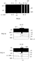
- the device D illustrated in figures 15-17 comprises a first active component C1 which constitutes a laser (or active lasing medium) and a second active component C2 which constitutes a modulator.
- the invention is not limited to the production of this type of device D. Indeed, it may comprise one active component, possibly coupled to integrated passive component(s), or two or more active components coupled together, and possibly coupled to integrated passive component(s).
- a device D according to the invention may comprise a laser and/or a modulator and/or a photodetector and/or an amplifier, possibly of the SOA type ("semiconductor optical amplifier"), for instance.
- each active component Ci is a semi-insulating buried heterostructure (or SIBH). But, this is not mandatory.
- This example of method comprises at least six steps.
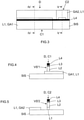
- a first step comprises growing a highly N doped layer L1 on a semi-insulating substrate SIS, and then layers L2-L4, which define together a vertical structure VS, on this highly N doped layer L1.
- the result of the implementation of this first step is illustrated in figures 1 and 2 .
- the vertical structure VS may comprise a N doped layer L2, an intrinsic layer L3 defining a waveguide, and a P doped layer L4.
- This first step can be done by means of an epitaxy.
- the highly N doped layer L1 can be also made of InP (InP-N+)
- layer L2 can be made of N doped InP
- layer L3 can be made of quaternary semiconductors (such as GaInAsP (Gallium Indium Arsenide Phosphide)) or of quantum wells (for instance made of sub-layers of Aluminium or Phosphorus)
- layer L4 can be made of P doped InP.
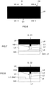
- a second step comprises etching the vertical structure VS (defined in the first step) in order to define at least one etched vertical structure VS'i set on top of a remaining part of the highly N doped layer L1 and an associated ground area GAi also with a remaining part of the highly N doped layer L1 (possibly the same than the one of the etched vertical structure VS'i).
- the etching aims at defining a first etched vertical structure VS'1 on top of a first remaining part of the highly N doped layer L1 and an associated first ground area GA1 with the same remaining part of the highly N doped layer L1, a second etched vertical structure VS'2 on top of a second remaining part of the highly N doped layer L1 and a second ground area GA2 with a third remaining part of the highly N doped layer L1.
- This second step can be done by means of an etching technique such as the reactive ion etching (or RIE). But other etching techniques may be used, and notably the ion beam etching (or IBE), the inductive coupled plasma etching (or ICPE) and the dry etching.
- etching technique such as the reactive ion etching (or RIE).
- IBE ion beam etching
- ICPE inductive coupled plasma etching
- dry etching dry etching
- a third step comprises growing a semi-insulating layer L5 on the free parts of the semi-insulating substrate SIS and on each ground area GAi and around each etched vertical structure VS'i. This growth is done up to the level of the top of each etched vertical structure VS'i.
- the semi-insulating layer L5 is preferably made of the same material as the semi-insulating substrate SIS.
- This third step (which is a regrowth) can be done by means of an epitaxy.
- a fourth step comprises growing a highly P doped layer L6 on the semi-insulating layer L6 and on top of each etched vertical structure VS'i.
- the highly P doped layer L6 can be also made of InP (InP-P+).
- This fourth step (which is a regrowth) can be done by means of an epitaxy.
- a fifth step comprises etching around each etched vertical structure VS'i till the level of the highly N doped layer L1, in order to define mesa strips constituting the active components Ci and to clear the top of each part of the highly N doped layer L1 that defines a ground area GAi associated to a mesa strip.
- This fifth step can be done by means of an etching technique such as the reactive ion etching (or RIE). But other etching techniques may be used, and notably the ion beam etching (or IBE), the inductive coupled plasma etching (or ICPE) and the dry etching.
- a first integrated control electrode E11 is deposited on top of the first mesa strip defining the laser C1
- a second integrated control electrode E21 is deposited on top of the second mesa strip defining the modulator C2.
- the device D comprises at least two etched vertical structures VS'i
- This aims at rendering the active components Ci electrically independent one from the other to avoid electrical cross talk (like leakage current and parasitic capacitance).
- the local isolation is represented by the rectangles referenced ZI, that are set on top of the highly P doped layer L6 in figure 9 .
- three isolation zones ZI have been created, a first one being located just after the end of the first integrated control electrode E11 in a transversal position, and second and third ones being respectively located just before and just after the second integrated control electrode E21 in transversal positions.
- This local electrical isolation can be carried out into the highly P doped layer L6 by means of a proton implantation in a part of at least each area that is located between two etched vertical structures VS'i.
- a proton implantation can be done by means of an accelerator of particles or a plasma generator.
- a sixth step comprises depositing a contact layer on top of a part of each ground area GAi to define integrated ground electrodes Ei2, and at least a part of another contact layer on top of a part of each mesa strip to fully or partly define integrated control electrodes Ei1.
- Each integrated ground electrode Ei2 and its associated integrated control electrode Ei1 are intended to allow control of the corresponding active component Ci that is constituted by a mesa strip.
- the integrated ground electrode E12 of the first component C1 (here a laser) is formed out of the mesa strip area to avoid parasitic capacitance (such as "fringe” capacitance) and leakage current for each component Ci.
- a large integrated ground electrode Ei2 is also formed out of its mesa strip.
- the electric field is applied only in the waveguide buried structure (layer L3) between the P-type layer L4 and the N-type layer L2 which is connected to the "ground ridge" part of layer L1 that is under the etched vertical structure VS'2.
- the device capacitance comes mainly from the ridge heterostructure (like in the Diode Ridge Technology), and the parasitic capacitance produced by the SIBH material is strongly reduced.
- the device according to embodiments proposed herein has a structure such that the ground electrode is located at a position which is not opposite to the position of the control electrode but the ground electrode is located on the structure of the device at a position which is offset from a position directly opposite to a position of the control electrode on the structure of the device.
- the control electrode is either not on the upper side (for example it may be on a lateral side) or if it is on the top side it is located at a location which is substantially away from a location (on the top side) facing the ground electrode.
- the insulation (and possibly passivation) layer L7 can be made of a benzo-cyclo-butene (BCB) polymer.
- BCB benzo-cyclo-butene
- Such an insulation (and possibly passivation) layer L7 further allows to increase the size of the integrated control electrodes Ei1 that are partly defined during the fifth step.
Landscapes
- Physics & Mathematics (AREA)
- Condensed Matter Physics & Semiconductors (AREA)
- General Physics & Mathematics (AREA)
- Electromagnetism (AREA)
- Optics & Photonics (AREA)
- Semiconductor Lasers (AREA)
Claims (11)
- Vorrichtung, die mindestens eine erste aktive optoelektronische Komponente (Ci) und eine zweite aktive optoelektronische Komponente (Ci) umfasst, wobei die ersten und zweiten aktiven Komponenten monolithisch auf einem halbisolierenden Substrat (Semi-Insulating Substrate - SIS) integriert sind, wobei die Vorrichtung ferner mindestens eine erste Elektrodenanordnung (Eij), die dazu ausgestaltet ist, die erste aktive optoelektronische Komponente (Ci) mittels eines Steuerstroms oder einer Steuerspannung zu steuern, und eine zweite Elektrodenanordnung (Eij) umfasst, die dazu ausgestaltet ist, die zweite aktive optoelektronische Komponente (Ci) mittels eines Steuerstroms oder einer Steuerspannung zu steuern, wobei jede von der ersten Steueranordnung und der zweiten Steueranordnung eine entsprechende Steuerelektrode und eine entsprechende Masseelektrode aufweist, wobei die erste aktive optoelektronische Komponente (Ci) eine erste vertikale Struktur (VS'i) umfasst und die zweite aktive optoelektronische Komponente (Ci) eine zweite vertikale Struktur (VS'i) umfasst, wobei die erste vertikale Struktur (VS'i) und die zweite vertikale Struktur (VS'i) derart durch Isolationszonen voneinander isoliert sind, dass eine erste Isolationszone (ZI) sich auf einer Seite einer Steuerelektrode befindet und eine zweite Isolationszone (ZI) sich auf einer anderen Seite der Steuerelektrode befindet, die der Seite der ersten Isolationszone (ZI) entgegengesetzt ist.
- Vorrichtung nach Anspruch 1, dadurch gekennzeichnet, dass jede aktive optoelektronische Komponente (Ci) eine halbisolierende vergrabene Heterostruktur ist.
- Vorrichtung nach einem der Ansprüche 1 und 2, dadurch gekennzeichnet, dass das Substrat ein halbisolierendes Indiumphosphidsubstrat (SIS) oder ein halbisolierendes Substrat (SIL) ist.
- Vorrichtung nach einem der vorhergehenden Ansprüche, die mindestens eine integrierte aktive optoelektronische Komponente umfasst, die aus einer Gruppe ausgewählt ist, die mindestens einen Laser, einen Modulator, einen Fotodetektor oder einen Verstärker umfasst.
- Vorrichtung nach einem der vorhergehenden Ansprüche, wobei die Masseelektrode sich auf der Struktur der Vorrichtung an einer Position befindet, die von einer Position versetzt ist, die einer Position der Steuerelektrode auf der Struktur der Vorrichtung direkt entgegengesetzt ist.
- Verfahren zur Herstellung von mindestens zwei aktiven optoelektronischen Komponenten (Ci) auf einem halbisolierenden Substrat (SIS), wobei die Herstellung einer ersten und zweiten aktiven optoelektronischen Komponente die folgenden Schritte umfasst:- Züchten einer hoch n-dotierten Schicht (L1) auf dem halbisolierenden Substrat (SIS) und dann von Schichten (L2 bis L4), die eine vertikale Struktur (VS) auf der hoch n-dotierten Schicht (L1) definieren,- Ätzen der vertikalen Struktur (VS), um mindestens eine geätzte vertikale Struktur (VS'i), die auf dem Oberteil eines übrigen Teils der hoch n-dotierten Schicht (L1) eingestellt ist, und einen zugehörigen Massebereich (GAi) auch mit einem übrigen Teil der hoch n-dotierten Schicht (L1) zu definieren,- Züchten einer halbisolierenden Schicht (L5) auf dem halbisolierenden Substrat (SIS) und auf jedem Massebereich (GAi) und um jede geätzte vertikale Struktur (VS'i),- Züchten einer hoch p-dotierten Schicht (L6) auf der halbisolierenden Schicht (L6) und auf dem Oberteil jeder geätzten vertikalen Struktur (VS'i),- Ätzen um jede geätzte vertikale Struktur (VS'i) bis zum Niveau der hoch n-dotierten Schicht (L1), um einen Mesa-Streifen zu definieren, der eine aktive optoelektronische Komponente (Ci) bildet, und um den Oberteil von jedem Teil der hoch n-dotierten Schicht (L1) freizumachen, wodurch ein Massebereich (GAi) definiert wird, der dem Mesa-Streifen zugehörig ist, und- Abscheiden einer Kontaktschicht auf dem Oberteil eines Teils von jedem Massebereich (GAi), um eine integrierte Masseelektrode (Ei2) zu definieren, und mindestens eines Teils einer anderen Kontaktschicht auf dem Oberteil eines Teils von jedem Mesa-Streifen, um eine integrierte Steuerelektrode (Ei1) zu definieren, die dazu ausgestaltet ist, die Steuerung der aktiven optoelektronischen Komponente (Ci) zu ermöglichen, die durch den Mesa-Streifen gebildet ist;wobei die erste aktive optoelektronische Komponente (Ci) eine erste geätzte vertikale Struktur (VS'i) umfasst und die zweite aktive optoelektronische Komponente (Ci) eine zweite geätzte vertikale Struktur (VS'i) umfasst, wobei die erste geätzte vertikale Struktur (VS'i) und die zweite geätzte vertikale Struktur (VS'i) derart voneinander durch Isolationszonen isoliert sind, dass eine erste Isolationszone (ZI) sich auf einer Seite einer Steuerelektrode befindet und eine zweite Isolationszone (ZI) sich auf einer anderen Seite der Steuerelektrode befindet, die der Seite der ersten Isolationszone (ZI) entgegengesetzt ist.
- Verfahren nach Anspruch 6, gekennzeichnet durch Abscheiden einer Kontaktschicht auf dem Oberteil von jedem Teil der hoch p-dotierten Schicht (L6), die auf dem Oberteil einer geätzten vertikalen Struktur (VS'i) eingestellt ist, um mindestens einen Teil der integrierten Steuerelektrode (Ei1) zu definieren, die der aktiven optoelektronischen Komponente zugehörig ist, die aus der geätzten vertikalen Struktur (VS'i) besteht, vor dem Ätzen um jede geätzte vertikale Struktur (VS'i).
- Verfahren nach Anspruch 6, gekennzeichnet durch Abscheiden der anderen Kontaktschicht auf dem Oberteil eines Teils von jedem Mesa-Streifen, um die integrierte Steuerelektrode (Ei1) vollständig zu definieren.
- Verfahren nach einem der Ansprüche 6 bis 8, gekennzeichnet durch Züchten einer Isolationsschicht (L7) auf dem Oberteil von jedem freigemachten Teil der hoch n-dotierten Schicht (L1), die sich auf einer Seite eines Mesa-Streifens befindet, vor dem Definieren von mindestens jeder zugehörigen integrierten Masseelektrode (Ei2).
- Verfahren nach Anspruch 9, dadurch gekennzeichnet, dass die Isolationsschicht (L7) ein Benzocyclobuten-Polymer ist.
- Verfahren nach einem der Ansprüche 6 bis 10, gekennzeichnet durch das Verwenden einer Ätztechnik, die ausgewählt ist aus einer Gruppe, die mindestens reaktives Ionenätzen, Ionenstrahlätzen, induktives gekoppeltes Plasmaätzen und Trockenätzen umfasst.
Priority Applications (1)
| Application Number | Priority Date | Filing Date | Title |
|---|---|---|---|
| EP20177053.4A EP3739635B1 (de) | 2010-06-30 | 2010-06-30 | Vorrichtung mit einer aktiven komponente und zugehörige elektroden sowie verfahren zur herstellung solch einer vorrichtung |
Applications Claiming Priority (2)
| Application Number | Priority Date | Filing Date | Title |
|---|---|---|---|
| EP20177053.4A EP3739635B1 (de) | 2010-06-30 | 2010-06-30 | Vorrichtung mit einer aktiven komponente und zugehörige elektroden sowie verfahren zur herstellung solch einer vorrichtung |
| EP20100290366 EP2402996A1 (de) | 2010-06-30 | 2010-06-30 | Vorrichtung mit einer aktiven Komponente und zugehörige Elektroden sowie Verfahren zur Herstellung solch einer Vorrichtung |
Related Parent Applications (1)
| Application Number | Title | Priority Date | Filing Date |
|---|---|---|---|
| EP20100290366 Division EP2402996A1 (de) | 2010-06-30 | 2010-06-30 | Vorrichtung mit einer aktiven Komponente und zugehörige Elektroden sowie Verfahren zur Herstellung solch einer Vorrichtung |
Publications (2)
| Publication Number | Publication Date |
|---|---|
| EP3739635A1 EP3739635A1 (de) | 2020-11-18 |
| EP3739635B1 true EP3739635B1 (de) | 2022-03-09 |
Family
ID=43003435
Family Applications (2)
| Application Number | Title | Priority Date | Filing Date |
|---|---|---|---|
| EP20100290366 Ceased EP2402996A1 (de) | 2010-06-30 | 2010-06-30 | Vorrichtung mit einer aktiven Komponente und zugehörige Elektroden sowie Verfahren zur Herstellung solch einer Vorrichtung |
| EP20177053.4A Active EP3739635B1 (de) | 2010-06-30 | 2010-06-30 | Vorrichtung mit einer aktiven komponente und zugehörige elektroden sowie verfahren zur herstellung solch einer vorrichtung |
Family Applications Before (1)
| Application Number | Title | Priority Date | Filing Date |
|---|---|---|---|
| EP20100290366 Ceased EP2402996A1 (de) | 2010-06-30 | 2010-06-30 | Vorrichtung mit einer aktiven Komponente und zugehörige Elektroden sowie Verfahren zur Herstellung solch einer Vorrichtung |
Country Status (1)
| Country | Link |
|---|---|
| EP (2) | EP2402996A1 (de) |
Families Citing this family (2)
| Publication number | Priority date | Publication date | Assignee | Title |
|---|---|---|---|---|
| JP5891920B2 (ja) * | 2012-04-16 | 2016-03-23 | 三菱電機株式会社 | 変調器集積型レーザ素子 |
| JP7835999B2 (ja) * | 2022-05-31 | 2026-03-26 | Ntt株式会社 | 光変調器および光送信器 |
Family Cites Families (11)
| Publication number | Priority date | Publication date | Assignee | Title |
|---|---|---|---|---|
| JP2686764B2 (ja) * | 1988-03-11 | 1997-12-08 | 国際電信電話株式会社 | 光半導体素子の製造方法 |
| EP0437836B1 (de) * | 1989-12-27 | 1995-05-17 | Nec Corporation | Optische Halbleitervorrichtung |
| US5287376A (en) * | 1992-12-14 | 1994-02-15 | Xerox Corporation | Independently addressable semiconductor diode lasers with integral lowloss passive waveguides |
| FR2706079B1 (fr) * | 1993-06-02 | 1995-07-21 | France Telecom | Composant intégré monolithique laser-modulateur à structure multi-puits quantiques. |
| FR2746215B1 (fr) * | 1996-03-12 | 1998-05-15 | Dispositif semiconducteur d'emission-reception a faible diaphotie | |
| US6526083B1 (en) * | 2001-10-09 | 2003-02-25 | Xerox Corporation | Two section blue laser diode with reduced output power droop |
| JP4055405B2 (ja) * | 2001-12-03 | 2008-03-05 | ソニー株式会社 | 電子部品及びその製造方法 |
| JP4622335B2 (ja) * | 2003-08-04 | 2011-02-02 | 日亜化学工業株式会社 | 半導体レーザ素子 |
| WO2005112096A1 (ja) * | 2004-05-18 | 2005-11-24 | Nippon Telegraph And Telephone Corporation | 導電性半導体基板上の電極パッド |
| JP4934271B2 (ja) * | 2004-06-11 | 2012-05-16 | 日本オプネクスト株式会社 | 単一電源駆動光集積装置 |
| JP4231854B2 (ja) * | 2005-03-17 | 2009-03-04 | アンリツ株式会社 | 半導体レーザ素子及びガス検知装置 |
-
2010
- 2010-06-30 EP EP20100290366 patent/EP2402996A1/de not_active Ceased
- 2010-06-30 EP EP20177053.4A patent/EP3739635B1/de active Active
Also Published As
| Publication number | Publication date |
|---|---|
| EP3739635A1 (de) | 2020-11-18 |
| EP2402996A1 (de) | 2012-01-04 |
Similar Documents
| Publication | Publication Date | Title |
|---|---|---|
| EP3306381B1 (de) | Optisches halbleitermodulationselement | |
| US8938134B2 (en) | Hybrid optical modulator for photonic integrated circuit devices | |
| US8948227B2 (en) | Isolated modulator electrodes for low power consumption | |
| DE112018000883T5 (de) | Elektrooptische Einheit mit III-V-Verstärkungsmaterialien und integriertemKühlkörper | |
| TWI632413B (zh) | 半導體光調變元件 | |
| US20050275053A1 (en) | Optical module device | |
| US6924918B2 (en) | Optical modulator and method of manufacturing the same | |
| US20140294335A1 (en) | Method for manufacturing semiconductor modulator and semiconductor modulator | |
| CN111129944B (zh) | 基于量子通信应用的电吸收光发射芯片及其制作方法 | |
| US8946842B2 (en) | Method for manufacturing optical waveguide receiver and optical waveguide receiver | |
| JP2003152264A (ja) | ナイトライド系半導体レーザを備えた光集積装置 | |
| EP3739635B1 (de) | Vorrichtung mit einer aktiven komponente und zugehörige elektroden sowie verfahren zur herstellung solch einer vorrichtung | |
| WO2007107782A1 (en) | Monolithically integrated optoelectronic components | |
| US7638856B2 (en) | Optoelectronic transmitter integrated circuit and method of fabricating the same using selective growth process | |
| US11791341B2 (en) | Radio-frequency loss reduction for integrated devices | |
| EP2403077B1 (de) | Photonische Vorrichtung und Verfahren zur Herstellung einer photonischen Vorrichtung | |
| EP3416252A1 (de) | Einstufige sibh für integrierte schaltungen | |
| CN121395044A (zh) | 一种vcsel和spad单片集成的芯片结构及其制备方法 | |
| CN121618317A (zh) | 一种混合波导高速率eml芯片结构及制备方法 |
Legal Events
| Date | Code | Title | Description |
|---|---|---|---|
| PUAI | Public reference made under article 153(3) epc to a published international application that has entered the european phase |
Free format text: ORIGINAL CODE: 0009012 |
|
| STAA | Information on the status of an ep patent application or granted ep patent |
Free format text: STATUS: THE APPLICATION HAS BEEN PUBLISHED |
|
| AC | Divisional application: reference to earlier application |
Ref document number: 2402996 Country of ref document: EP Kind code of ref document: P |
|
| AK | Designated contracting states |
Kind code of ref document: A1 Designated state(s): AL AT BE BG CH CY CZ DE DK EE ES FI FR GB GR HR HU IE IS IT LI LT LU LV MC MK MT NL NO PL PT RO SE SI SK SM TR |
|
| STAA | Information on the status of an ep patent application or granted ep patent |
Free format text: STATUS: REQUEST FOR EXAMINATION WAS MADE |
|
| 17P | Request for examination filed |
Effective date: 20210518 |
|
| RBV | Designated contracting states (corrected) |
Designated state(s): AL AT BE BG CH CY CZ DE DK EE ES FI FR GB GR HR HU IE IS IT LI LT LU LV MC MK MT NL NO PL PT RO SE SI SK SM TR |
|
| GRAP | Despatch of communication of intention to grant a patent |
Free format text: ORIGINAL CODE: EPIDOSNIGR1 |
|
| STAA | Information on the status of an ep patent application or granted ep patent |
Free format text: STATUS: GRANT OF PATENT IS INTENDED |
|
| INTG | Intention to grant announced |
Effective date: 20211008 |
|
| GRAS | Grant fee paid |
Free format text: ORIGINAL CODE: EPIDOSNIGR3 |
|
| GRAA | (expected) grant |
Free format text: ORIGINAL CODE: 0009210 |
|
| STAA | Information on the status of an ep patent application or granted ep patent |
Free format text: STATUS: THE PATENT HAS BEEN GRANTED |
|
| AC | Divisional application: reference to earlier application |
Ref document number: 2402996 Country of ref document: EP Kind code of ref document: P |
|
| AK | Designated contracting states |
Kind code of ref document: B1 Designated state(s): AL AT BE BG CH CY CZ DE DK EE ES FI FR GB GR HR HU IE IS IT LI LT LU LV MC MK MT NL NO PL PT RO SE SI SK SM TR |
|
| REG | Reference to a national code |
Ref country code: CH Ref legal event code: EP Ref country code: AT Ref legal event code: REF Ref document number: 1474869 Country of ref document: AT Kind code of ref document: T Effective date: 20220315 |
|
| REG | Reference to a national code |
Ref country code: IE Ref legal event code: FG4D |
|
| REG | Reference to a national code |
Ref country code: DE Ref legal event code: R096 Ref document number: 602010068103 Country of ref document: DE |
|
| REG | Reference to a national code |
Ref country code: LT Ref legal event code: MG9D |
|
| REG | Reference to a national code |
Ref country code: NL Ref legal event code: MP Effective date: 20220309 |
|
| PG25 | Lapsed in a contracting state [announced via postgrant information from national office to epo] |
Ref country code: SE Free format text: LAPSE BECAUSE OF FAILURE TO SUBMIT A TRANSLATION OF THE DESCRIPTION OR TO PAY THE FEE WITHIN THE PRESCRIBED TIME-LIMIT Effective date: 20220309 Ref country code: NO Free format text: LAPSE BECAUSE OF FAILURE TO SUBMIT A TRANSLATION OF THE DESCRIPTION OR TO PAY THE FEE WITHIN THE PRESCRIBED TIME-LIMIT Effective date: 20220609 Ref country code: LT Free format text: LAPSE BECAUSE OF FAILURE TO SUBMIT A TRANSLATION OF THE DESCRIPTION OR TO PAY THE FEE WITHIN THE PRESCRIBED TIME-LIMIT Effective date: 20220309 Ref country code: HR Free format text: LAPSE BECAUSE OF FAILURE TO SUBMIT A TRANSLATION OF THE DESCRIPTION OR TO PAY THE FEE WITHIN THE PRESCRIBED TIME-LIMIT Effective date: 20220309 Ref country code: BG Free format text: LAPSE BECAUSE OF FAILURE TO SUBMIT A TRANSLATION OF THE DESCRIPTION OR TO PAY THE FEE WITHIN THE PRESCRIBED TIME-LIMIT Effective date: 20220609 |
|
| REG | Reference to a national code |
Ref country code: AT Ref legal event code: MK05 Ref document number: 1474869 Country of ref document: AT Kind code of ref document: T Effective date: 20220309 |
|
| PG25 | Lapsed in a contracting state [announced via postgrant information from national office to epo] |
Ref country code: LV Free format text: LAPSE BECAUSE OF FAILURE TO SUBMIT A TRANSLATION OF THE DESCRIPTION OR TO PAY THE FEE WITHIN THE PRESCRIBED TIME-LIMIT Effective date: 20220309 Ref country code: GR Free format text: LAPSE BECAUSE OF FAILURE TO SUBMIT A TRANSLATION OF THE DESCRIPTION OR TO PAY THE FEE WITHIN THE PRESCRIBED TIME-LIMIT Effective date: 20220610 Ref country code: FI Free format text: LAPSE BECAUSE OF FAILURE TO SUBMIT A TRANSLATION OF THE DESCRIPTION OR TO PAY THE FEE WITHIN THE PRESCRIBED TIME-LIMIT Effective date: 20220309 |
|
| PG25 | Lapsed in a contracting state [announced via postgrant information from national office to epo] |
Ref country code: NL Free format text: LAPSE BECAUSE OF FAILURE TO SUBMIT A TRANSLATION OF THE DESCRIPTION OR TO PAY THE FEE WITHIN THE PRESCRIBED TIME-LIMIT Effective date: 20220309 |
|
| PG25 | Lapsed in a contracting state [announced via postgrant information from national office to epo] |
Ref country code: SM Free format text: LAPSE BECAUSE OF FAILURE TO SUBMIT A TRANSLATION OF THE DESCRIPTION OR TO PAY THE FEE WITHIN THE PRESCRIBED TIME-LIMIT Effective date: 20220309 Ref country code: SK Free format text: LAPSE BECAUSE OF FAILURE TO SUBMIT A TRANSLATION OF THE DESCRIPTION OR TO PAY THE FEE WITHIN THE PRESCRIBED TIME-LIMIT Effective date: 20220309 Ref country code: RO Free format text: LAPSE BECAUSE OF FAILURE TO SUBMIT A TRANSLATION OF THE DESCRIPTION OR TO PAY THE FEE WITHIN THE PRESCRIBED TIME-LIMIT Effective date: 20220309 Ref country code: PT Free format text: LAPSE BECAUSE OF FAILURE TO SUBMIT A TRANSLATION OF THE DESCRIPTION OR TO PAY THE FEE WITHIN THE PRESCRIBED TIME-LIMIT Effective date: 20220711 Ref country code: ES Free format text: LAPSE BECAUSE OF FAILURE TO SUBMIT A TRANSLATION OF THE DESCRIPTION OR TO PAY THE FEE WITHIN THE PRESCRIBED TIME-LIMIT Effective date: 20220309 Ref country code: EE Free format text: LAPSE BECAUSE OF FAILURE TO SUBMIT A TRANSLATION OF THE DESCRIPTION OR TO PAY THE FEE WITHIN THE PRESCRIBED TIME-LIMIT Effective date: 20220309 Ref country code: CZ Free format text: LAPSE BECAUSE OF FAILURE TO SUBMIT A TRANSLATION OF THE DESCRIPTION OR TO PAY THE FEE WITHIN THE PRESCRIBED TIME-LIMIT Effective date: 20220309 Ref country code: AT Free format text: LAPSE BECAUSE OF FAILURE TO SUBMIT A TRANSLATION OF THE DESCRIPTION OR TO PAY THE FEE WITHIN THE PRESCRIBED TIME-LIMIT Effective date: 20220309 |
|
| PG25 | Lapsed in a contracting state [announced via postgrant information from national office to epo] |
Ref country code: PL Free format text: LAPSE BECAUSE OF FAILURE TO SUBMIT A TRANSLATION OF THE DESCRIPTION OR TO PAY THE FEE WITHIN THE PRESCRIBED TIME-LIMIT Effective date: 20220309 Ref country code: IS Free format text: LAPSE BECAUSE OF FAILURE TO SUBMIT A TRANSLATION OF THE DESCRIPTION OR TO PAY THE FEE WITHIN THE PRESCRIBED TIME-LIMIT Effective date: 20220709 Ref country code: AL Free format text: LAPSE BECAUSE OF FAILURE TO SUBMIT A TRANSLATION OF THE DESCRIPTION OR TO PAY THE FEE WITHIN THE PRESCRIBED TIME-LIMIT Effective date: 20220309 |
|
| REG | Reference to a national code |
Ref country code: DE Ref legal event code: R097 Ref document number: 602010068103 Country of ref document: DE |
|
| PLBE | No opposition filed within time limit |
Free format text: ORIGINAL CODE: 0009261 |
|
| STAA | Information on the status of an ep patent application or granted ep patent |
Free format text: STATUS: NO OPPOSITION FILED WITHIN TIME LIMIT |
|
| PG25 | Lapsed in a contracting state [announced via postgrant information from national office to epo] |
Ref country code: MC Free format text: LAPSE BECAUSE OF FAILURE TO SUBMIT A TRANSLATION OF THE DESCRIPTION OR TO PAY THE FEE WITHIN THE PRESCRIBED TIME-LIMIT Effective date: 20220309 Ref country code: DK Free format text: LAPSE BECAUSE OF FAILURE TO SUBMIT A TRANSLATION OF THE DESCRIPTION OR TO PAY THE FEE WITHIN THE PRESCRIBED TIME-LIMIT Effective date: 20220309 |
|
| REG | Reference to a national code |
Ref country code: CH Ref legal event code: PL |
|
| 26N | No opposition filed |
Effective date: 20221212 |
|
| REG | Reference to a national code |
Ref country code: BE Ref legal event code: MM Effective date: 20220630 |
|
| PG25 | Lapsed in a contracting state [announced via postgrant information from national office to epo] |
Ref country code: SI Free format text: LAPSE BECAUSE OF FAILURE TO SUBMIT A TRANSLATION OF THE DESCRIPTION OR TO PAY THE FEE WITHIN THE PRESCRIBED TIME-LIMIT Effective date: 20220309 |
|
| PG25 | Lapsed in a contracting state [announced via postgrant information from national office to epo] |
Ref country code: LU Free format text: LAPSE BECAUSE OF NON-PAYMENT OF DUE FEES Effective date: 20220630 Ref country code: LI Free format text: LAPSE BECAUSE OF NON-PAYMENT OF DUE FEES Effective date: 20220630 Ref country code: IE Free format text: LAPSE BECAUSE OF NON-PAYMENT OF DUE FEES Effective date: 20220630 Ref country code: CH Free format text: LAPSE BECAUSE OF NON-PAYMENT OF DUE FEES Effective date: 20220630 |
|
| PG25 | Lapsed in a contracting state [announced via postgrant information from national office to epo] |
Ref country code: BE Free format text: LAPSE BECAUSE OF NON-PAYMENT OF DUE FEES Effective date: 20220630 |
|
| PG25 | Lapsed in a contracting state [announced via postgrant information from national office to epo] |
Ref country code: IT Free format text: LAPSE BECAUSE OF FAILURE TO SUBMIT A TRANSLATION OF THE DESCRIPTION OR TO PAY THE FEE WITHIN THE PRESCRIBED TIME-LIMIT Effective date: 20220309 |
|
| PG25 | Lapsed in a contracting state [announced via postgrant information from national office to epo] |
Ref country code: MK Free format text: LAPSE BECAUSE OF FAILURE TO SUBMIT A TRANSLATION OF THE DESCRIPTION OR TO PAY THE FEE WITHIN THE PRESCRIBED TIME-LIMIT Effective date: 20220309 Ref country code: CY Free format text: LAPSE BECAUSE OF FAILURE TO SUBMIT A TRANSLATION OF THE DESCRIPTION OR TO PAY THE FEE WITHIN THE PRESCRIBED TIME-LIMIT Effective date: 20220309 |
|
| PG25 | Lapsed in a contracting state [announced via postgrant information from national office to epo] |
Ref country code: HU Free format text: LAPSE BECAUSE OF FAILURE TO SUBMIT A TRANSLATION OF THE DESCRIPTION OR TO PAY THE FEE WITHIN THE PRESCRIBED TIME-LIMIT; INVALID AB INITIO Effective date: 20100630 |
|
| PG25 | Lapsed in a contracting state [announced via postgrant information from national office to epo] |
Ref country code: TR Free format text: LAPSE BECAUSE OF FAILURE TO SUBMIT A TRANSLATION OF THE DESCRIPTION OR TO PAY THE FEE WITHIN THE PRESCRIBED TIME-LIMIT Effective date: 20220309 |
|
| PG25 | Lapsed in a contracting state [announced via postgrant information from national office to epo] |
Ref country code: MT Free format text: LAPSE BECAUSE OF FAILURE TO SUBMIT A TRANSLATION OF THE DESCRIPTION OR TO PAY THE FEE WITHIN THE PRESCRIBED TIME-LIMIT Effective date: 20220309 |
|
| REG | Reference to a national code |
Ref country code: DE Ref legal event code: R079 Ref document number: 602010068103 Country of ref document: DE Free format text: PREVIOUS MAIN CLASS: H01L0029410000 Ipc: H10D0064200000 |
|
| PGFP | Annual fee paid to national office [announced via postgrant information from national office to epo] |
Ref country code: DE Payment date: 20250507 Year of fee payment: 16 |
|
| PGFP | Annual fee paid to national office [announced via postgrant information from national office to epo] |
Ref country code: GB Payment date: 20250508 Year of fee payment: 16 |
|
| PGFP | Annual fee paid to national office [announced via postgrant information from national office to epo] |
Ref country code: FR Payment date: 20250508 Year of fee payment: 16 |