EP3731031A1 - High resolution time capture circuit and corresponding device, capture method and computer program product - Google Patents
High resolution time capture circuit and corresponding device, capture method and computer program product Download PDFInfo
- Publication number
- EP3731031A1 EP3731031A1 EP20170811.2A EP20170811A EP3731031A1 EP 3731031 A1 EP3731031 A1 EP 3731031A1 EP 20170811 A EP20170811 A EP 20170811A EP 3731031 A1 EP3731031 A1 EP 3731031A1
- Authority
- EP
- European Patent Office
- Prior art keywords
- capt
- cnt
- sub
- capture
- clk
- Prior art date
- Legal status (The legal status is an assumption and is not a legal conclusion. Google has not performed a legal analysis and makes no representation as to the accuracy of the status listed.)
- Granted
Links
Images


Classifications
-
- H—ELECTRICITY
- H03—ELECTRONIC CIRCUITRY
- H03M—CODING; DECODING; CODE CONVERSION IN GENERAL
- H03M1/00—Analogue/digital conversion; Digital/analogue conversion
- H03M1/12—Analogue/digital converters
- H03M1/50—Analogue/digital converters with intermediate conversion to time interval
- H03M1/502—Analogue/digital converters with intermediate conversion to time interval using tapped delay lines
-
- G—PHYSICS
- G06—COMPUTING OR CALCULATING; COUNTING
- G06F—ELECTRIC DIGITAL DATA PROCESSING
- G06F1/00—Details not covered by groups G06F3/00 - G06F13/00 and G06F21/00
- G06F1/04—Generating or distributing clock signals or signals derived directly therefrom
- G06F1/08—Clock generators with changeable or programmable clock frequency
-
- G—PHYSICS
- G04—HOROLOGY
- G04F—TIME-INTERVAL MEASURING
- G04F10/00—Apparatus for measuring unknown time intervals by electric means
- G04F10/04—Apparatus for measuring unknown time intervals by electric means by counting pulses or half-cycles of an AC
-
- H—ELECTRICITY
- H03—ELECTRONIC CIRCUITRY
- H03K—PULSE TECHNIQUE
- H03K21/00—Details of pulse counters or frequency dividers
- H03K21/02—Input circuits
-
- H—ELECTRICITY
- H03—ELECTRONIC CIRCUITRY
- H03K—PULSE TECHNIQUE
- H03K5/00—Manipulating of pulses not covered by one of the other main groups of this subclass
- H03K5/159—Applications of delay lines not covered by the preceding subgroups
-
- H—ELECTRICITY
- H03—ELECTRONIC CIRCUITRY
- H03K—PULSE TECHNIQUE
- H03K3/00—Circuits for generating electric pulses; Monostable, bistable or multistable circuits
- H03K3/01—Details
- H03K3/012—Modifications of generator to improve response time or to decrease power consumption
Definitions
- Embodiments of the present disclosure relate to solutions concerning high resolution time capture circuit.
- the present disclosure in particular refers to techniques for performing high resolution capture of input signal in a device, e.g. an integrated circuit, in particular a microcontroller, in particular microcontrollers for automotive/industrial high-end applications.
- a device e.g. an integrated circuit, in particular a microcontroller, in particular microcontrollers for automotive/industrial high-end applications.
- Time capture circuits are known, which measure time between events, in particular edges, of a logic input signal.
- most of the applications including some automotive applications, require a resolution in the timing control of the order of a few hundred picoseconds.
- This high resolution in timing control is beneficial in high accuracy digital control applications such as LED lighting, motor control and power conversion.
- a high resolution input capture function improve the control accuracy for period/duty cycle measurements of pulses train cycles, instantaneous speed/frequency measurements, voltage measurements across an isolation boundary and distance/sonar measurement and scanning.
- the required resolution is generally higher than the maximum resolution allowable from the microcontroller (MCU) operating clock frequency and currently there is no known solution except increasing the operating clock frequency.
- MCU microcontroller
- one or more of the above objectives is achieved by means of a time capture circuit having the features specifically set forth in the claims that follow.
- Embodiments moreover concern a related electronic device, method and computer program product.
- the present disclosure relates to a time capture circuit to measure time between events, in particular edges, of a logic input signal, comprising a delay line receiving at its input said input signal and generating a plurality of consecutive increasingly delayed replicas of said logic input signal, each replica delayed by a fixed delay with respect to the preceding replica, a free running counter which is clocked by a counter clock signal corresponding to an external clock signal multiplied by a clock scale factor and supplies a counter value to a counter value capture block, said counter value capture block receiving also said input signal and being configured to capture said counter value upon the occurrence of an event in said input signal outputting a captured counter value and issuing a trigger signal, a decoder module receiving as inputs said input signal, said plurality of delayed replicas and said captured counter value and said trigger signal, said decoder module being configured to determine a decoded value on the basis of at least the values of said input signal and of said plurality of consecutive increasingly replicas when the trigger signal is issued and to compute a capture value as the difference of
- said delay line comprise a number of delay circuits equal to two raised to a power of a given integer size factor and said second scale factor is equal to said integer size factor minus the first scale factor.
- said circuit includes a configuration register configured to supply said first scale factor to said counter value capture module and to said decoder module and to supply said clock scale factor to said counter clock.
- said decoder module accesses a first decoding table comprising records, in particular rows, including as fields, in particular column, the values of the external signal and of the other delayed replicas at the capture event corresponding to external signal event, and the corresponding decoded value, which value is correspondence with a capture interval in which the external signal event occurs.
- said decoder module is further configured to compare periodically with the frequency of a respective clock the current value of said input signal and of said plurality of consecutive increasingly replicas with the ones acquired during the previous clock period to identify value changes and in the positive, if at least one of the values is changed, to issue a feedback trigger signal to the counter value capture block to store the counter value, unless the current value of said input signal and of said plurality of consecutive increasingly replicas are all zeros or all ones.
- the decoder accesses an enhanced decoder table which includes a further field indicating the result of said comparison with respect to the external signal and a further field indicating a capture length value.
- said enhanced decoder table associates records corresponding to said first decoder table to a conventional value of capture length and to a positive result of said comparison for the external signal, and sets of records associated to a negative result of said comparison for the external signal and to respective different values of capture length storing in each record the values taken by the external signal and delayed replicas at the capture event occurs in one of the capture intervals.
- the present disclosure relates also to an electronic device comprising:
- the present disclosure relates also to a method for time capture to measure time between events, in particular edges, of a logic input signal, comprising inputting to a delay line said input signal generating a plurality of consecutive increasingly delayed replicas of said signal, each replica delayed by a fixed delay with respect to the preceding replica, operating a free running counter clocked by counter clock signal corresponding to an external clock signal multiplied by a clock scale factor and supplies a counter value to a counter value capture block capturing said counter value upon the occurrence of an event in said input signal and outputting a captured counter value and issuing a trigger signal, determining, in particular at a decoder module, determine a decoded value on the basis of the values of said input signal and said plurality of consecutive increasingly replicas when said trigger signal is issued and computing a capture value as the difference of said captured counter value logical left shifted by a first scale factor and said decoded value logical right shifted by a second scale factor.
- the method includes setting said clock scale factor to one.
- the present disclosure relates also to a computer program product directly loadable into the internal memory of a digital computer, comprising software code portions.
- figure 1 it is shown an embodiment of the solution here described.
- a time capture circuit 20 which receives as input signal an external signal EXT_SGL corresponding to the external signal to be monitored, e.g. a PWM (Pulse Width Modulation) signal with variable period and/or variable duty cycle.
- the time capture circuit 20 is comprised for instance in an electronic device 10, e.g. a microcontroller or other integrated chip circuit.
- the time capture circuit 20 is thus clocked by a system clock signal CLK_SYS, e.g. the clock of the whole device on which the circuit 20 operates.
- the external signal EXT_SGL can be a signal generated by the device 10 or fed to device 10 from another device.
- the external signal EXT_SGL enters a delay line D, which includes a sequence of delay blocks introducing a same fixed delay, D1,...,Dm,..., D M with m consecutive integer index varying between 1 and a number M.
- the sequence of delay blocks introducing a same fixed delay D1,...,Dm,..., D M determine a corresponding plurality consecutive increasingly delayed replicas of said input signal, D1 out , ..., Dm out ,..., DM out , each m-th replica delayed by a fixed delay T Dm with respect to the preceding (m-1)-th replica.
- the external signal EXT_SGL is internally routed to sub-modules CNT, CAPT_CNT, where sub-module CNT is a counter and a CAPT_CNT a capture module able to capture the counter value of counter CNT on events occurring in the external signal EXT_SGL.
- the counter CNT is clocked by clock counter module CLK_CNT with a respective clock counter signal CLK_CNT_out which corresponds to the ratio of the system clock CLK_SYS to a value CLK_CNT_PRS selected by a configuration register CONF_REG.
- configuration register CONF_REG can a register of the electronic device 10 or set by the electronic device 10.
- the counter CNT is a free-running counter.
- the counter capture module CAPT_CNT which also receives the external signal EXT_SGL, is configured to capture, i.e. store, a counter value x of the counter CNT on a event of the external signal EXT_SGL, e.g. on a rising edge, on a falling edge or both, and issues a corresponding trigger signal CAPT_CNT trg to a capture decode module CAPT_DECODE.
- the counter capture module CAPT_CNT in the same time also sends a captured value CAPT_CNT out , which corresponds to the captured counter value x to the capture decode module CAPT_DECODE.
- the capture feature of the counter capture module CAPT_CNT is configurable by the configuration register CONF_REG.
- the high-resolution capture feature of the circuit 20 can be activated by selecting in the configuration register CONF_REG the value of a first scale parameter, CKL_CAPT_PRS, supplied to the capture decode module CAPT_DECODE, greater than zero.
- the first scale parameter CKL_CAPT_PRS can assume the value 0, 1, ..., N, N being the given integer size factor which sets the size of the delay line D.
- CLK_SYS_RES is the clock system resolution, i.e. the time between two consecutive edges of the system clock signal CLK_SYS.
- the time capture circuit 20 can operate also if CLK_CNT_PRS > 1, however to operate the circuit 20 with an input clock frequency lower than the system clock could produce a reduction of the power consumption, e.g. the circuit could be used to have the same resolution of the system clock but with a lower input clock.
- the capture decode module CAPT_DECODE on a new capture event i.e. the trigger CAPT_CNT trg signal coming from the counter capture module CAPT_CNT
- HR_CAPT_VAL CAPT_CNT out ⁇ ⁇ CKL_CAPT_PRS ⁇ CAPT_DCD
- the capture interval of index 0 is the nearest in time to a capture event C, corresponding to the issuance of the trigger CAPT_CNT_trg by the counter capture module CAPT_CNT.
- CAPT_DCD indicates a decoded value calculated, in particular obtained, by the decode module CAPT_DECODE by a decoded table DT, exemplified here below in Table 1, assuming that the time length of the EXT_SGL level (high or low logic level) is greater than the decoded value CAPT_DCD.
- the capture value HR_CAPT_VAL is the difference of said captured counter value CAPT_CNT out logical left shifted by a first scale factor CKL_CAPT_PRS, i.e. multiplied, and said decoded value CAPT_DCD logical right shifted by a second scale factor.
- Table 1 representing the decoding table DT used by the decoder module CAPT_DECODE to obtain the decoded value CAPT_DCD.
- Table 1 is a data structure including a number of records, in the example the table rows, which include in a field, i.e. a column, the decoded value CAPT_DCD, and in the following fields, specifically columns, the values of the external signal, indicated as zero delayed replica DOout and of the other M-1 delayed replicas D1out...DMout at the issuance of the trigger signal CAPT_CNT trg , following an event E (E1, E2, in figure 2 ) i.e. at the capture event C (C1, C2 in figure 2 ).
- the external signal value DOout can be logical zero or logical one, depending on the event E of the external signal EXT_SGL issuing the trigger signal CAPT_CNT trg .
- the value in the decoding table DT corresponding to the delayed replicas D1out...DMout are indicated as D 0, i.e. they have the same level of D0out, or D 0 , they have the negated logic level. Given a set of this ordered values of D0out...DMout from the Table 1, which is for instance a look-up table stored in the decoder module CAPT_DECODE, the corresponding decoded value CAPT_DCD is obtained.
- the decoder table DT is built by using the values of the external signal, indicated as zero delayed replica DOout and of the other M-1 delayed replicas D1out...DMout as access input value to obtain the decoded value CAPT_DCD.
- the circuit 20 includes a decoder module CAPT_DECODE accessing a first decoding table DT comprising records, in particular rows, including as fields, in particular columns, the values of the external signal DOout and of the other delayed replicas D1out...DMout at the capture event C corresponding to external signal event E, and the corresponding decoded value CAPT_DCD, which value is in correspondence with a capture interval in which the external signal event E occurs. It is underlined that such correspondence can be different if the capture interval is indexed differently with respect to the decoded value CAPT_DCD, e.g. from the farthest interval (10) from capture C to the nearest (IM) instead of from the nearest (10) to the farthest.
- CAPT_DECODE accessing a first decoding table DT comprising records, in particular rows, including as fields, in particular columns, the values of the external signal DOout and of the other delayed replicas D1out...DMout at the capture event C corresponding to external signal event E, and the corresponding decoded value
- Table 2 CAPT_ DCD D 0out D 1out D 2out D 3out 0 0/1 D 0 D 0 D 0 1 0/1 D 0 D 0 D 0 2 0/1 D 0 D 0 D 0 3 0/1 D 0 D 0 D 0 D 0
- FIG 2 it is shown a time diagram referred to such example, in which, as a function of time t are indicated the signals D0 or EXT_SGL, D1, D2, D3, the counter value CNT and the counter clock CLK_CNT.
- C1 indicates a first capture event
- C2 indicates a second capture event.
- the external signal EXT_SGL presents a first rising edge, e.g. a first event, E1
- the first capture event C1 happens, i.e. the counter capture module CAPT_CNT, which also receives the external signal EXT_SGL, stores the counter value x of the counter CNT on the event E1, i.e.
- the capture event C1 signals the moment the signals D0out, D1out, D2out, D3out are evaluated to access the decoder table DT and obtain the decoded value CAPT_DCD.
- the intervals are thus 10...13, starting from the nearest to capture event C.
- the constraint on the minimum time length of the EXT_SGL level can be removed.
- FIG 5 it is thus shown a further embodiment of the solution here described, which includes a time capture circuit 20', which removes the constraint on the minimum time length of the EXT_SGL level.
- the architecture of the circuit 20' corresponds substantially to the one of circuit 20', the main difference being that the decoder module CAPT_DECODE is configured to compare periodically (i.e.
- the decoder module CAPT_DECODE sends a feedback trigger signal CAPT_DECODE trg to the capture counter module CAPT_CNT commanding to store the counter value CNT.
- the decoder module CAPT_DECODE calculates the decode value CAPT_DCD and the capture length CAPT_LEN value by an enhanced table EDT an embodiment of which is represented in Table 3 shown here below.
- Such Table 3 similarly to Table 1, has records, in particular organized in rows, and in the first field, i.e. column has the decoded value CAPT_DCD, and in the following columns the values of the external signal, indicated as zero delayed replica D0out, and of the other M-1 delayed replicas D1out...DMout.
- Column includes two further fields, i.e. columns, a column for the capture length CAPT_LEN value, which is obtained together with the decoded value CAPT_DCD, and a column indicating if the criterion D 0out ⁇ D 0 PRE , is satisfied, in particular by indicating yes Y or no N.
- the time length of the input signal is greater than the decoded CAPT_DCD value and the length CAPT_LEN value must not be calculated.
- the capture length CAPT_LEN assumes a conventional value, e.g. zero.
- the duration of the current (i.e. new) value of the external signal EXT_SGL is detected also by the counter capture module CAPT_CNT satisfying the constraint on the minimum time length of the external signal EXT_SGL level.
- this general case falls into the previous case and the Table 3 is reduced to the Table 1.
- the tables have a decreasing number of rows increasing the value of CAPT_LEN, since for each value of CAPT_LEN, the minimum value of CAPT_DCD cannot be less than the value of CAPT LEN in order to not satisfy the criterion D 0out ⁇ D 0 PRE .
- the circuit 20 includes an enhanced decoder table EDT which associates records, i.e. rows, corresponding to said first decoder table DT to a conventional value of capture length CAP_LEN, in particular zero, and to a positive result of the comparison for the external signal D0 ( D 0out ⁇ D 0 PRE ), while sets of records are associated to a negative result ( D. 0out ⁇ D 0 PRE ) and to respective different values of capture length CAP_LEN storing in each record the values taken by the external signal DOout and delayed replicas D1out...DMout at the capture event C when the event E occurs in one of the capture intervals Im.
- EDT enhanced decoder table EDT which associates records, i.e. rows, corresponding to said first decoder table DT to a conventional value of capture length CAP_LEN, in particular zero, and to a positive result of the comparison for the external signal D0 ( D 0out ⁇ D 0 PRE ), while sets of records are associated to a negative result (
- FIG 5 it is shown a time diagram similar to those of figure 2 and 3 referred to such example, in which therefore the capture length CAPT_LEN between edges E1, E2 is shorter than the minimum length, i.e. the decoded value CAPT_DCD.
- Figure 6 represents instead a time diagram in the case of a different longer capture length CAPT_LEN between edges E1, E2, always shorter than the minimum length.
- the decoder module CAPT_DECODE accesses an enhanced decoded table EDT to obtain a capture value and a capture length value.
- M 15
- the solutions just described improve the capture feature resolution without increasing the operating clock frequency of the electronic device hosting the capture circuit, e.g. the microcontroller, avoiding the drawbacks in term of power consumption and noise emission/sensitivity.
Landscapes
- Engineering & Computer Science (AREA)
- Physics & Mathematics (AREA)
- Theoretical Computer Science (AREA)
- General Physics & Mathematics (AREA)
- General Engineering & Computer Science (AREA)
- Power Engineering (AREA)
- Nonlinear Science (AREA)
- Manipulation Of Pulses (AREA)
- Electrophonic Musical Instruments (AREA)
- Measuring Pulse, Heart Rate, Blood Pressure Or Blood Flow (AREA)
- Ultra Sonic Daignosis Equipment (AREA)
- Compression, Expansion, Code Conversion, And Decoders (AREA)
Abstract
Description
- Embodiments of the present disclosure relate to solutions concerning high resolution time capture circuit.
- The present disclosure in particular refers to techniques for performing high resolution capture of input signal in a device, e.g. an integrated circuit, in particular a microcontroller, in particular microcontrollers for automotive/industrial high-end applications.
- Time capture circuits are known, which measure time between events, in particular edges, of a logic input signal. In this context, most of the applications, including some automotive applications, require a resolution in the timing control of the order of a few hundred picoseconds. This high resolution in timing control is beneficial in high accuracy digital control applications such as LED lighting, motor control and power conversion. For example, a high resolution input capture function improve the control accuracy for period/duty cycle measurements of pulses train cycles, instantaneous speed/frequency measurements, voltage measurements across an isolation boundary and distance/sonar measurement and scanning.
- With regards to the input capture functions, the required resolution is generally higher than the maximum resolution allowable from the microcontroller (MCU) operating clock frequency and currently there is no known solution except increasing the operating clock frequency.
- The design of a time capture circuit working with a frequency clock higher than the frequency clock of the whole device presents drawbacks in term of module die size, power consumption and noise emission/sensitivity.
- In view of the above, it is an objective of the present disclosure to provide solutions which overcome one or more of the above drawbacks.
- According to one or more embodiments, one or more of the above objectives is achieved by means of a time capture circuit having the features specifically set forth in the claims that follow. Embodiments moreover concern a related electronic device, method and computer program product.
- The claims are an integral part of the technical teaching of the disclosure provided herein.
- As mentioned before, the present disclosure relates to a time capture circuit to measure time between events, in particular edges, of a logic input signal, comprising
a delay line receiving at its input said input signal and generating a plurality of consecutive increasingly delayed replicas of said logic input signal, each replica delayed by a fixed delay with respect to the preceding replica,
a free running counter which is clocked by a counter clock signal corresponding to an external clock signal multiplied by a clock scale factor and supplies a counter value to a counter value capture block,
said counter value capture block receiving also said input signal and being configured to capture said counter value upon the occurrence of an event in said input signal outputting a captured counter value and issuing a trigger signal,
a decoder module receiving as inputs said input signal, said plurality of delayed replicas and said captured counter value and said trigger signal,
said decoder module being configured to determine a decoded value on the basis of at least the values of said input signal and of said plurality of consecutive increasingly replicas when the trigger signal is issued and to compute a capture value as the difference of said captured counter value logical left shifted by a first scale factor and said decoded value logical right shifted by a second scale factor. - In variant embodiments, said delay line comprise a number of delay circuits equal to two raised to a power of a given integer size factor and said second scale factor is equal to said integer size factor minus the first scale factor.
- In variant embodiments said circuit includes a configuration register configured to supply said first scale factor to said counter value capture module and to said decoder module and to supply said clock scale factor to said counter clock.
- In variant embodiments, said decoder module accesses a first decoding table comprising records, in particular rows, including as fields, in particular column, the values of the external signal and of the other delayed replicas at the capture event corresponding to external signal event, and the corresponding decoded value, which value is correspondence with a capture interval in which the external signal event occurs.
- In variant embodiments, said decoder module is further configured to compare periodically with the frequency of a respective clock the current value of said input signal and of said plurality of consecutive increasingly replicas with the ones acquired during the previous clock period to identify value changes and in the positive, if at least one of the values is changed, to issue a feedback trigger signal to the counter value capture block to store the counter value, unless the current value of said input signal and of said plurality of consecutive increasingly replicas are all zeros or all ones.
- In variant embodiments, the decoder accesses an enhanced decoder table which includes a further field indicating the result of said comparison with respect to the external signal and a further field indicating a capture length value.
- In variant embodiments, said enhanced decoder table associates records corresponding to said first decoder table to a conventional value of capture length and to a positive result of said comparison for the external signal, and sets of records associated to a negative result of said comparison for the external signal and to respective different values of capture length storing in each record the values taken by the external signal and delayed replicas at the capture event occurs in one of the capture intervals.
- The present disclosure relates also to an electronic device comprising:
- a time capture circuit to measure time between events, in particular edges, of a logic input signal, comprising
- a delay line receiving at its input said input signal and generating a plurality of consecutive increasingly delayed replicas of said logic input signal, each replica delayed by a fixed delay with respect to the preceding replica,
- a free running counter which is clocked by a counter clock signal corresponding to an external clock signal multiplied by a clock scale factor and supplies a counter value to a counter value capture block,
- said counter value capture block receiving also said input signal and being configured to capture said counter value upon the occurrence of an event in said input signal outputting a captured counter value and issuing a trigger signal,
- a decoder module receiving as inputs said input signal, said plurality of delayed replicas and said captured counter value and said trigger signal,
- said decoder module being configured to determine a decoded value on the basis of at least the values of said input signal and of said plurality of consecutive increasingly replicas when the trigger signal is issued and to compute a capture value as the difference of said captured counter value logical left shifted by a first scale factor and said decoded value logical right shifted by a second scale factor.
- The present disclosure relates also to a method for time capture to measure time between events, in particular edges, of a logic input signal,
comprising inputting to a delay line said input signal generating a plurality of consecutive increasingly delayed replicas of said signal, each replica delayed by a fixed delay with respect to the preceding replica,
operating a free running counter clocked by counter clock signal corresponding to an external clock signal multiplied by a clock scale factor and supplies a counter value to a counter value capture block capturing said counter value upon the occurrence of an event in said input signal and outputting a captured counter value and issuing a trigger signal,
determining, in particular at a decoder module, determine a decoded value on the basis of the values of said input signal and said plurality of consecutive increasingly replicas when said trigger signal is issued and computing a capture value as the difference of said captured counter value logical left shifted by a first scale factor and said decoded value logical right shifted by a second scale factor. - In variant embodiment the method includes setting said clock scale factor to one.
- The present disclosure relates also to a computer program product directly loadable into the internal memory of a digital computer, comprising software code portions.
- Embodiments of the present disclosure will now be described with reference to the annexed drawings, which are provided purely by way of non-limiting example and in which:
-
Figure 1 is a schematic circuit diagram of an embodiment of the solution here described; -
Figures 2 and 3 are time diagrams of signals formed in the embodiment offigure 1 in different operating conditions; -
Figure 4 is a schematic circuit diagram of a further embodiment of the solution here described; -
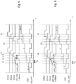
Figure 5 and 6 are time diagrams of signals formed in the embodiment offigure 4 in different operating conditions - In the following description, numerous specific details are given to provide a thorough understanding of embodiments. The embodiments can be practiced without one or several specific details, or with other methods, components, materials, etc. In other instances, well-known structures, materials, or operations are not shown or described in detail to avoid obscuring aspects of the embodiments.
- Reference throughout this specification to "one embodiment" or "an embodiment" means that a particular feature, structure, or characteristic described in connection with the embodiment is included in at least one embodiment. Thus, the appearances of the phrases "in one embodiment" or "in an embodiment" in various places throughout this specification are not necessarily all referring to the same embodiment. Furthermore, the particular features, structures, or characteristics may be combined in any suitable manner in one or more embodiments.
- The headings provided herein are for convenience only and do not interpret the scope or meaning of the embodiments.
- In
figure 1 it is shown an embodiment of the solution here described. - In
figure 1 it is thus shown atime capture circuit 20 which receives as input signal an external signal EXT_SGL corresponding to the external signal to be monitored, e.g. a PWM (Pulse Width Modulation) signal with variable period and/or variable duty cycle. Thetime capture circuit 20 is comprised for instance in anelectronic device 10, e.g. a microcontroller or other integrated chip circuit. Thetime capture circuit 20 is thus clocked by a system clock signal CLK_SYS, e.g. the clock of the whole device on which thecircuit 20 operates. The external signal EXT_SGL can be a signal generated by thedevice 10 or fed todevice 10 from another device. - The external signal EXT_SGL enters a delay line D, which includes a sequence of delay blocks introducing a same fixed delay, D1,...,Dm,..., DM with m consecutive integer index varying between 1 and a number M. The number M, i.e. the number of delay circuits blocks in the delay line D, is equal to two raise to power of a given integer size factor N, i.e. M = 2N-1. The sequence of delay blocks introducing a same fixed delay D1,...,Dm,..., DM determine a corresponding plurality consecutive increasingly delayed replicas of said input signal, D1out, ..., Dm out,..., DMout, each m-th replica delayed by a fixed delay TDm with respect to the preceding (m-1)-th replica. The delay time length TDm is:

- The external signal EXT_SGL is internally routed to sub-modules CNT, CAPT_CNT, where sub-module CNT is a counter and a CAPT_CNT a capture module able to capture the counter value of counter CNT on events occurring in the external signal EXT_SGL.
- The counter CNT is clocked by clock counter module CLK_CNT with a respective clock counter signal CLK_CNT_out which corresponds to the ratio of the system clock CLK_SYS to a value CLK_CNT_PRS selected by a configuration register CONF_REG. Such configuration register CONF_REG can a register of the
electronic device 10 or set by theelectronic device 10. - More in detail, the counter CNT is a free-running counter. The counter capture module CAPT_CNT, which also receives the external signal EXT_SGL, is configured to capture, i.e. store, a counter value x of the counter CNT on a event of the external signal EXT_SGL, e.g. on a rising edge, on a falling edge or both, and issues a corresponding trigger signal CAPT_CNTtrg to a capture decode module CAPT_DECODE. The counter capture module CAPT_CNT in the same time also sends a captured value CAPT_CNTout, which corresponds to the captured counter value x to the capture decode module CAPT_DECODE. The capture feature of the counter capture module CAPT_CNT is configurable by the configuration register CONF_REG. The counter CNT is clocked by the clock counter module CLK_CNT generating a clock CLK_CNToutput with a frequency equal or lower than the frequency of the system clock, i.e. CLK_CNToutput = CLK_SYS/CLK_CNT_PRS where CLK_CNT_PRS = 2q with q = 0, 1, ..., Q, which is a positive integer clock pre-scaler parameter selected by the configuration register CONF_REG.
- If it is CLK_CNTout=CLK_SYS, (i.e. the clock pre-scaler parameter CLK_CNT_PRS = 1), thus the counter CNT is clocked at the same clock frequency of the system, CLK_SYS, the high-resolution capture feature of the
circuit 20 can be activated by selecting in the configuration register CONF_REG the value of a first scale parameter, CKL_CAPT_PRS, supplied to the capture decode module CAPT_DECODE, greater than zero. The first scale parameter CKL_CAPT_PRS can assume thevalue 0, 1, ..., N, N being the given integer size factor which sets the size of the delay line D. A capture resolution of the module HR_CAPT is:
- CLK_SYS_RES is the clock system resolution, i.e. the time between two consecutive edges of the system clock signal CLK_SYS.
- It is underlined that in general the
time capture circuit 20 can operate also if CLK_CNT_PRS > 1, however to operate thecircuit 20 with an input clock frequency lower than the system clock could produce a reduction of the power consumption, e.g. the circuit could be used to have the same resolution of the system clock but with a lower input clock. In this case the resolution CLK_SYS_RES can be replaced in the formulas with CLK_CNT_RES = CLK_SYS_RES * CLK_CNT_PRS. - If the first scale parameter CKL_CAPT_PRS is equal to the integer size factor N, the capture decode module CAPT_DECODE on a new capture event (i.e. the trigger CAPT_CNTtrg signal coming from the counter capture module CAPT_CNT) reads the output value CAPT_CNTout of the counter capture module CAPT_CNT and outputs values of signals D0out, D1out, ..., DMout of the external signal EXT_SGL = D0 and of the delay blocks D1,..., DM and it calculates a high resolution capture value HR_CAPT_VAL as:

- The clock interval of the system clock CLK_SYS, which correspond to the counter clock CNT_CLK, can be thus seen as divided in 2CKL_CAPT_PRS capture intervals, Im, m=0... 2CKL_CAPT_PRS-1. If CKL_CAPT_PRS is equal to the integer size factor N, m=0...M. The capture interval of index 0 is the nearest in time to a capture event C, corresponding to the issuance of the trigger CAPT_CNT_trg by the counter capture module CAPT_CNT.
- CAPT_DCD indicates a decoded value calculated, in particular obtained, by the decode module CAPT_DECODE by a decoded table DT, exemplified here below in Table 1, assuming that the time length of the EXT_SGL level (high or low logic level) is greater than the decoded value CAPT_DCD.
- If first scale parameter CKL_CAPT_PRS is lower than the integer size factor N, the decoder module CAPT_DECODE calculates the capture value HR_CAPT_VAL with a more general expression as:

- In other words the capture value HR_CAPT_VAL is the difference of said captured counter value CAPT_CNTout logical left shifted by a first scale factor CKL_CAPT_PRS, i.e. multiplied, and said decoded value CAPT_DCD logical right shifted by a second scale factor.
- Here below it is shown Table 1, representing the decoding table DT used by the decoder module CAPT_DECODE to obtain the decoded value CAPT_DCD. Such table is a data structure including a number of records, in the example the table rows, which include in a field, i.e. a column, the decoded value CAPT_DCD, and in the following fields, specifically columns, the values of the external signal, indicated as zero delayed replica DOout and of the other M-1 delayed replicas D1out...DMout at the issuance of the trigger signal CAPT_CNTtrg, following an event E (E1, E2, in
figure 2 ) i.e. at the capture event C (C1, C2 infigure 2 ). - The external signal value DOout can be logical zero or logical one, depending on the event E of the external signal EXT_SGL issuing the trigger signal CAPT_CNTtrg. The value in the decoding table DT corresponding to the delayed replicas D1out...DMout are indicated as D0, i.e. they have the same level of D0out, or
D0 , they have the negated logic level. Given a set of this ordered values of D0out...DMout from the Table 1, which is for instance a look-up table stored in the decoder module CAPT_DECODE, the corresponding decoded value CAPT_DCD is obtained.Table 1 CAPT DCD D0out D1out D2out Dmout DM-1out DMout 0 0/1 D0 D0 ... D 0 D0 1 0/1 D0 D0 ... D 0 D0 2 0/1 D0 D0 ... D0 D0 ... ... ... ... ... ... ... M-1 0/1 D0 D0 ... D0 D0 M 0/1 D0 D0 ... D0 D0 - The decoder table DT is built by using the values of the external signal, indicated as zero delayed replica DOout and of the other M-1 delayed replicas D1out...DMout as access input value to obtain the decoded value CAPT_DCD. The decoder table DT is in particular built by storing in each row the values taken by the external signal DOut and delayed replicas D0out...DMout at the capture event C, e.g. C1, corresponding to the occurrence of an event, e.g. rising edge E1 in one of the capture intervals Im. If Im=I0, i.e. the rising edge E1 happens just before the capture event C1, CAPT_DCD is correspondingly 0, if Im=IM, CAPT_DCD=M.
- In other words, the
circuit 20 includes a decoder module CAPT_DECODE accessing a first decoding table DT comprising records, in particular rows, including as fields, in particular columns, the values of the external signal DOout and of the other delayed replicas D1out...DMout at the capture event C corresponding to external signal event E, and the corresponding decoded value CAPT_DCD, which value is in correspondence with a capture interval in which the external signal event E occurs. It is underlined that such correspondence can be different if the capture interval is indexed differently with respect to the decoded value CAPT_DCD, e.g. from the farthest interval (10) from capture C to the nearest (IM) instead of from the nearest (10) to the farthest. - Considering a first example, for N = 2, M = 2N - 1 = 3 and TD1 = TD2 = TD3 = 1/(4∗fCLK_SYS) according to the formula (1), CKL_CAPT_PRS = 2, HR_CAPT_RES = CLK_SYS_RES/4 according to the formula (2).
- The values of the decoder table DT for this example are shown in Table 2 here below.
Table 2 CAPT_ DCD D0out D1out D2out D3out 0 0/1 D 0 D0 D0 1 0/1 D 0 D0 D0 2 0/1 D0 D0 D0 3 0/1 D0 D0 D0 - In
figure 2 it is shown a time diagram referred to such example, in which, as a function of time t are indicated the signals D0 or EXT_SGL, D1, D2, D3, the counter value CNT and the counter clock CLK_CNT. C1 indicates a first capture event, C2 indicates a second capture event. As it can be seen the external signal EXT_SGL presents a first rising edge, e.g. a first event, E1, and at the next clock period of the counter clock CLK_CNT the first capture event C1 happens, i.e. the counter capture module CAPT_CNT, which also receives the external signal EXT_SGL, stores the counter value x of the counter CNT on the event E1, i.e. the rising edge, and issues the corresponding trigger signal CAPT_CNTtrg to the capture decode module CAPT_DECODE. Therefore the capture event C1 signals the moment the signals D0out, D1out, D2out, D3out are evaluated to access the decoder table DT and obtain the decoded value CAPT_DCD. - In
Figure 2 are shown also the capture intervals Im in which the period T of the counter clock CNT_CLK is subdivided for capture according to the resulting sampling resolution Tres, i.e. the time amplitude of the intervals Im, which having set the first scale parameter CKL_CAPT_PRS by the configuration register CONF_REG equal to 2, e.g. equal to N, imposes HR_CAPT_RES = CLK_SYS_RES/4 thus the sampling resolution time Tres is 1/4 of the clock period, CNT_CLK, i.e. by choosing the first scale parameter equal to the size parameter the minimum sampling resolution time is obtained. The intervals are thus 10...13, starting from the nearest to capture event C. - Referring to
Figure 2 and to Table 2, on the first capture event C1, the decoded value CAPT_DCD is equal to 2 (D0=1, D1=1= D0, D2=1= D0, D3=0≠ D0) and HR_CAPT_VAL = (x<<2) - (2>>0) according to the formula (3), while on the second capture event C2, falling edge of EXT-SGL, CAPT_DCD = 1 (D0 = 0, D1 = 0 = D1, D2 = 1 ≠ D0, D3 = 1 ≠ D0) and HR_CAPT_VAL = ((x + 2) << 2) - (1 >> 0) according to the formula (3). - Considering a second example, for N = 2, M = 2N - 1 = 3 and TD1 = TD2 = TD3 = 1/(4∗fCLK_SYS) according to the formula (1), if CKL_CAPT_PRS = 1 i.e. lower than the size parameter N, HR_CAPT_RES = CLK_SYS_RES/2 according to the formula (2). Referring to the
Figure 3 , which shows a time diagram for the second example analogous to the one offigure 2 , and to Table 2, on the first capture event C1 CAPT_DCD = 2 (D0=1, D1=1=D0, D2=1=D0, D3=0#D0) and HR_CAPT_VAL = (x<<1) - (2>>1) = (x<<1) - 1 according to the formula (4), while on the second capture event C2 CAPT_DCD = 1 (D0=0, D1=0=D0, D2=1≠D0, D3=1≠D0) and HR_CAPT_VAL = ((x + 2)<<1) - (1>>1) = ((x + 2)<<1) - 0 according to the formula (4). - In
figure 3 it is shown the sampling resolution Tres, which having set the first scale parameter CKL_CAPT_PRS by the configuration register CONF_REG equal to 1, e.g. lower than N, imposes HR_CAPT_RES = CLK_SYS_RES/2 thus the sampling resolution time Tres is greater than the minimum sampling resolution time, i.e. 1/2 of the clock period, CNT_CLK. - In further embodiments, the constraint on the minimum time length of the EXT_SGL level can be removed.
- In
figure 5 it is thus shown a further embodiment of the solution here described, which includes a time capture circuit 20', which removes the constraint on the minimum time length of the EXT_SGL level. The architecture of the circuit 20' corresponds substantially to the one of circuit 20', the main difference being that the decoder module CAPT_DECODE is configured to compare periodically (i.e. with the frequency of its clock, which is the counter clock CLK_CNT, as shown infigure 1 and5 the current output values D0out, D1out,..., DMout of the external signal EXT_SGL = D0 and of the delay blocks D1,..., DM with the ones present at the previous period of the counter clock CLK_CNT, and, if at least one of the values is changed (i.e. a new event is occurred) the decoder module CAPT_DECODE sends a feedback trigger signal CAPT_DECODEtrg to the capture counter module CAPT_CNT commanding to store the counter value CNT. If the current output values D0out, D1out, ..., DMout are all zeros or all ones (in the latter e.g. signal level normally high with CAPT LEN referred to duration of low level), even if there is one or more changes, the event is discarded (e.g. event D1 infigure 5 ). - On each not-discarded event, the sub-module CAPT_DECODE calculates the capture value HR_CAPT_VAL using the formula (4) and a length HR_CAPT_LEN, i.e. the time length of the level of the external signal EXT_SGL, i.e. the time between the two edges E1, E2, as:

- In this embodiment, the decoder module CAPT_DECODE calculates the decode value CAPT_DCD and the capture length CAPT_LEN value by an enhanced table EDT an embodiment of which is represented in Table 3 shown here below.
- Such Table 3, similarly to Table 1, has records, in particular organized in rows, and in the first field, i.e. column has the decoded value CAPT_DCD, and in the following columns the values of the external signal, indicated as zero delayed replica D0out, and of the other M-1 delayed replicas D1out...DMout. However includes two further fields, i.e. columns, a column for the capture length CAPT_LEN value, which is obtained together with the decoded value CAPT_DCD, and a column indicating if the criterion D0out≠D0PRE, is satisfied, in particular by indicating yes Y or no N.
Table 3 CAPT_ DCD CAPT_ LEN D0out ≠ D0PRE [N=NO, Y=YES] D0out D1out D2out Dmout DM-1 out DMout 0 0 Y 0/1 D0 D0 ... D 0 D0 1 0 Y 0/1 D0 D0 ... D 0 D0 2 0 Y 0/1 D0 D0 ... D0 D0 ... 0 Y ... ... ... ... ... ... M-1 0 Y 0/1 D0 D0 ... D0 D0 M 0 Y 0/1 D0 D0 ... D 0 D0 1 1 N 0/1 D0 D0 ... D 0 D0 2 1 N 0/1 D0 D0 ... D0 D0 ... ... ... ... ... ... ... ... ... M-1 1 N 0/1 D0 D0 ... D0 D0 M 1 N 0/1 D0 D0 ... D 0 D0 2 2 N 0/1 D0 D0 ... D0 D0 ... ... ... ... ... ... ... ... ... M-1 2 N 0/1 D0 D0 ... D0 D0 M 2 N 0/1 D0 D0 ... D0 D0 ... ... ... ... ... ... ... ... ... M-1 M-1 N 0/1 D0 D0 ... D0 D0 M M-1 N 0/1 D0 D0 ... D0 D0 M M N 0/1 D0 D0 ... D0 D0 - If the D0 ≠ D0PRE where D0 is the current value of the external signal EXT_SGL and D0PRE is the previous value, the time length of the input signal is greater than the decoded CAPT_DCD value and the length CAPT_LEN value must not be calculated. In this case the capture length CAPT_LEN assumes a conventional value, e.g. zero.
- In other word, the duration of the current (i.e. new) value of the external signal EXT_SGL is detected also by the counter capture module CAPT_CNT satisfying the constraint on the minimum time length of the external signal EXT_SGL level. As result, this general case falls into the previous case and the Table 3 is reduced to the Table 1.
- The enhanced table EDT is built by providing the same decode table DT if D0out ≠ D0PRE, while if D0out = D0PRE, for each value of CAPT_LEN is added a corresponding table of values, by storing in each row the values taken by the external signal DOout and delayed replicas D1out...DMout at the capture event C, e.g. C1, corresponding to the occurrence of an event, e.g. rising edge E1 in one of the capture intervals Im and by considering that CAPT_LEN can be less or equal to CAPT_DCD otherwise D0out ≠ D0PRE
- The tables have a decreasing number of rows increasing the value of CAPT_LEN, since for each value of CAPT_LEN, the minimum value of CAPT_DCD cannot be less than the value of CAPT LEN in order to not satisfy the criterion D0out ≠ D0PRE.
- In other words, the
circuit 20 includes an enhanced decoder table EDT which associates records, i.e. rows, corresponding to said first decoder table DT to a conventional value of capture length CAP_LEN, in particular zero, and to a positive result of the comparison for the external signal D0 (D0out ≠ D0PRE), while sets of records are associated to a negative result (D.0out ≠ D0PRE) and to respective different values of capture length CAP_LEN storing in each record the values taken by the external signal DOout and delayed replicas D1out...DMout at the capture event C when the event E occurs in one of the capture intervals Im. - Considering a practical example, for N = 2, M = 2N - 1 = 3 and TD1 = TD2 = TD3 = 1 / (4 ∗ fCLK_SYS) according to the formula (1). If CKL_CAPT_PRS is set equal to 2, i.e. equal to N, HR_CAPT_RES = CLK_SYS_RES/4 according to the formula (2).
- In
figure 5 it is shown a time diagram similar to those offigure 2 and 3 referred to such example, in which therefore the capture length CAPT_LEN between edges E1, E2 is shorter than the minimum length, i.e. the decoded value CAPT_DCD. - The values of the decoder table for this example are shown in Table 4 here below.
Table 4 CAPT_DCD CAPT_LEN D0 ≠ D0PRE [N = NO, Y = YES] D0out D1out D2out D3out 0 0 Y 0/1 D 0 D0 D0 1 0 Y 0/1 D 0 D0 D0 2 0 Y 0/1 D0 D0 D0 3 0 Y 0/1 D 0 D0 D0 1 1 N 0/1 D 0 D0 D0 2 1 N 0/1 D0 D0 D0 3 1 N 0/1 D 0 D0 D0 2 2 N 0/1 D0 D0 D0 3 2 N 0/1 D0 D0 D0 3 3 N 0/1 D0 D0 D0 - Referring to the
Figure 5 and to the Table 4, on the first capture event C1, CAPT_DCD = 2 (D0 = 0, D1 = 1 ≠ D0, D2 = 1 ≠ D0, D3 = 0 ≠ D0), HR_CAPT_VAL = (x << 2) - (2 >> 0) according to the formula (3) and HR_CAPT_LEN = CAPT_LEN = 2, while on the second capture event C2 CAPT_DCD = 3 (D0 = 0, D1 = 0 = D0, D2 = 0 ≠ D0, D3 = 1 ≠ D0) and HR_CAPT_VAL = ((x + 2) << 2) - (3 >> 0) according to the formula (3) and HR_CAPT_LEN = CAPT_LEN = 1. -
Figure 6 represents instead a time diagram in the case of a different longer capture length CAPT_LEN between edges E1, E2, always shorter than the minimum length. - Referring to the
Figure 6 and to the Table 4, on the first capture event CAPT_DCD = 3 (D0 = 0, D1 = 1 ≠ D0, D2 = 1 ≠ D0, D3 = 1 ≠ D0), HR_CAPT_VAL = (x << 2) - (3 >> 0) according to the formula (3) and HR_CAPT_LEN = CAPT_LEN = 3, while on the second capture event CAPT_DCD = 3 (D0 = 0, D1 = 0 = D0, D2 = 1 ≠ D0, D3 = 1 ≠ D0) and HR_CAPT_VAL = ((x + 2) << 2) - (3 >> 0) according to the formula (3) and HR_CAPT_LEN = CAPT_LEN = 2. - Thus, in the circuit 20' of
Figure 4 the decoder module CAPT_DECODE accesses an enhanced decoded table EDT to obtain a capture value and a capture length value. - An embodiment of the
circuit 20/20' can operate with a maximum external clock frequency, CLK_SYSMAX = 400MHz. The minimum required resolution can be 200ps, which determines that the minimum value of number M of delay circuits blocks in the delay line D is MMIN = 1/(200ps ∗ 400MHz) - 1 = 12.5. Thus by selecting the size parameter N as 4, M=15, TDm = 1/ (16 ∗ CLK_SYSMAX) = 156.25ps. - The solutions disclosed herein have thus significant advantages with respect to the known solutions.
- The solutions just described improve the capture feature resolution without increasing the operating clock frequency of the electronic device hosting the capture circuit, e.g. the microcontroller, avoiding the drawbacks in term of power consumption and noise emission/sensitivity.
- Of course, without prejudice to the principle of the invention, the details of construction and the embodiments may vary widely with respect to what has been described and illustrated herein purely by way of example, without thereby departing from the scope of the present invention, as defined by the ensuing claims.
Claims (11)
- A time capture circuit (20, 20') to measure time between events, in particular edges, of a logic input signal (EXT_SGL, D0), comprising
a delay line (D) receiving at its input said input signal (EXT_SGL, D0) and generating a plurality of consecutive increasingly delayed replicas (D1out,..., Dmout,..., DMout) of said logic input signal (EXT_SGL, D0), each replica (Dmout) delayed by a fixed delay (TDm) with respect to the preceding replica (Dm-1out),
a free running counter (CNT) which is clocked by a counter clock signal (CNT_CLK) corresponding to an external clock signal (CLK_SYS) multiplied by a clock scale factor (CLK_CNT_PRS) and supplies a counter value (x) to a counter value capture block (CAPT_CNT),
said counter value capture block (CAPT_CNT) receiving also said input signal (EXT_SGL, D0) and being configured to capture said counter value (x) upon the occurrence of an event (E1, E2, C1, C2) in said input signal outputting a captured counter value (CAPT_CNTout) and issuing a trigger signal (CAPT-CNTtrg),
a decoder module (CAPT_DECODE) receiving as inputs said input signal (EXT_SGL, D0), said plurality of delayed replicas (D1out,...,Dmout,..., DMout) and said captured counter value (CAPT_CNTout) and said trigger signal (CAPT_CNTtrg),
said decoder module (CAPT_DECODE) being configured to determine a decoded value (CAPT_DCD)) on the basis of at least the values of said input signal (EXT_SGL, D0) and of said plurality of consecutive increasingly replicas (D1out,...,Dmout,..., DMout) when the trigger signal (CAPT_CNTtrg) is issued and to compute a capture value (HRS_CAPT_VAL) as the difference of said captured counter value (CAPT_CNTout) logical left shifted by a first scale factor (CLK_CAPT_PRS) and said decoded value (CAPT_DCD) logical right shifted by a second scale factor (N- CLK_CAPT_PRS). - The circuit according to Claim 1, wherein said delay line (D) comprise a number (M) of delay circuits (D1,...,Dm,..., DM) equal to two raise to a power of a given integer size factor (N) and said second scale factor (N-CLK_CAPT_PRS) is equal to said integer size factor (N) minus the first scale factor (CLK_CAPT_PRS).
- The circuit according to Claim 1, wherein includes a configuration register (CONF_REG) configured to supply said first scale factor (CLK_CAPT_PRS) to said counter value capture module (CAPT_CNT) and to said decoder module (CAPT_DECODE) and to supply said clock scale factor (CLK_CNT_PRS) to said counter clock (CNT_CLK).
- The circuit according to Claim 1, wherein said decoder module (CAPT_DECODE) accesses a first decoding table (DT) comprising records, in particular rows, including as fields, in particular column, the values of the external signal (DOout) and of the other delayed replicas (D1out...DMout) at the capture event (C) corresponding to external signal event (E), and the corresponding decoded value CAPT_DCD, which value is correspondence with a capture interval in which the external signal event (E) occurs.
- The circuit of any of the previous claims from 1 to 4 wherein said decoder module (CAPT_DECODE) is further configured to compare periodically with the frequency of a respective clock (CNT_CLK) the current value of said input signal (EXT_SGL, D0) and of said plurality of consecutive increasingly replicas (D1out,...,Dmout,..., DMout) with the ones acquired during the previous clock period to identify value changes and in the positive, if at least one of the values is changed, to issue a feedback trigger signal (CAPT_DECODEtrg) to the counter value capture block (CAPT_CNT) to store the counter value (x), unless the current value of said input signal (EXT_SGL, D0) and of said plurality of consecutive increasingly replicas (D1out, ..., Dmout, ..., DMout) are all zeros or all ones.
- The circuit according to Claim 4 and 5, wherein the decoder accesses an enhanced decoder table (EDT) which includes a further field indicating the result of said comparison with respect to the external signal (D0 ≠ D0PRE) and a further field indicating a capture length value (CAP_LEN).
- The circuit according to Claim 6, wherein said enhanced decoder table (EDT) associates records corresponding to said first decoder table (DT) to a conventional value of capture length (CAP LEN) and to a positive result of said comparison for the external signal (D0), and sets of records associated to a negative result of said comparison for the external signal and to respective different values of capture length (CAP_LEN) storing in each record the values taken by the external signal (DOut) and delayed replicas (D0out...DMout) at the capture event (C) when the event (E) occurs in one of the capture intervals (Im).
- An electronic device comprising:a time capture circuit (20, 20') to measure time between events, in particular edges, of a logic input signal (EXT_SGL, D0), comprisinga delay line (D) receiving at its input said input signal (EXT_SGL, D0) and generating a plurality of consecutive increasingly delayed replicas (D1out, ..., Dmout, ..., DMout) of said logic input signal (EXT_SGL, D0), each replica (Dmout) delayed by a fixed delay (Tdm) with respect to the preceding replica (Dm-1out),a free running counter (CNT) which is clocked by a counter clock signal (CNT_CLK) corresponding to an external clock signal (CLK_SYS) multiplied by a clock scale factor (CLK_CNT_PRS) and supplies a counter value (x) to a counter value capture block (CAPT_CNT),said counter value capture block (CAPT_CNT) receiving also said input signal (EXT_SGL, D0) and being configured to capture said counter value (x) upon the occurrence of an event (E1, E2; C1, C2) in said input signal outputting a captured counter value (CAPT_CNTout) and issuing a trigger signal (CAPT_CNTtrg),a decoder module (CAPT_DECODE) receiving as inputs said input signal (EXT_SGL, D0), said plurality of delayed replicas (D1out, ..., Dmout, ..., DMout) and said captured counter value (CAPT_CNTout) and said trigger signal (CAPT_CNTtrg),said decoder module (CAPT_DECODE) being configured to determine a decoded value (CAPT_DCD)) on the basis of at least the values of said input signal (EXT_SGL, D0) and of said plurality of consecutive increasingly replicas (D1out, ..., Dmout, ..., DMout) when the trigger signal (CAPT_CNTtrg) is issued and to compute a capture value (HRS_CAPT_VAL) as the difference of said captured counter value (CAPT_CNTout) logical left shifted by a first scale factor (CLK_CAPT_PRS) and said decoded value (CAPT_DCD) logical right shifted by a second scale factor (N- CLK_CAPT_PRS).
- A method for time capture to measure time between event, in particular edges, of a logic input signal (EXT_SGL, D0),
comprising inputting to a delay line (D) said input signal (EXT_SGL, D0) generating a plurality of consecutive increasingly delayed replicas (D1out,...,Dmout,..., DMout) of said signal, each replica delayed by a fixed delay (TDm) with respect to the preceding replica,
operating a free running counter (CNT) clocked by counter clock signal corresponding to an external clock signal multiplied by a clock scale factor and supplies a counter value to a counter value capture block capturing said counter value upon the occurrence of an event in said input signal (EXT_SGL, D0) and outputting a captured counter value and issuing a trigger signal,
determining, in particular at a decoder module, determine a decoded value on the basis of the values of said input signal (EXT_SGL, D0) and said plurality of consecutive increasingly replicas when said trigger signal is issued and computing a capture value as the difference of said captured counter value logical left shifted by a first scale factor and said decoded value logical right shifted by a second scale factor. - The method of claim 9, including setting said clock scale factor (CLK_CNT_PRS) to one.
- Computer program product directly loadable into the internal memory of a digital computer, comprising software code portions for performing the steps of the method of claim 9 or 10.
Applications Claiming Priority (1)
| Application Number | Priority Date | Filing Date | Title |
|---|---|---|---|
| IT102019000006396A IT201900006396A1 (en) | 2019-04-26 | 2019-04-26 | HIGH TEMPORAL RESOLUTION CAPTURE CIRCUIT AND CORRESPONDING DEVICE, CAPTURE PROCEDURE AND IT PRODUCT |
Publications (2)
| Publication Number | Publication Date |
|---|---|
| EP3731031A1 true EP3731031A1 (en) | 2020-10-28 |
| EP3731031B1 EP3731031B1 (en) | 2025-12-17 |
Family
ID=67384290
Family Applications (1)
| Application Number | Title | Priority Date | Filing Date |
|---|---|---|---|
| EP20170811.2A Active EP3731031B1 (en) | 2019-04-26 | 2020-04-22 | High resolution time capture circuit and corresponding device, capture method and computer program product |
Country Status (3)
| Country | Link |
|---|---|
| US (1) | US11204620B2 (en) |
| EP (1) | EP3731031B1 (en) |
| IT (1) | IT201900006396A1 (en) |
Citations (4)
| Publication number | Priority date | Publication date | Assignee | Title |
|---|---|---|---|---|
| EP0300757A2 (en) * | 1987-07-21 | 1989-01-25 | Logic Replacement Technology Limited | Time measurement apparatus |
| US20100141240A1 (en) * | 2008-12-08 | 2010-06-10 | Andrew Hutchinson | Methods for determining the frequency or period of a signal |
| US20120319751A1 (en) * | 2009-04-17 | 2012-12-20 | Texas Instruments Incorporated | High resolution capture |
| US20170149418A1 (en) * | 2015-11-20 | 2017-05-25 | Texas Instruments Incorporated | High Resolution Capture |
Family Cites Families (5)
| Publication number | Priority date | Publication date | Assignee | Title |
|---|---|---|---|---|
| US6826247B1 (en) * | 2000-03-24 | 2004-11-30 | Stmicroelectronics, Inc. | Digital phase lock loop |
| US20060269030A1 (en) * | 2005-05-26 | 2006-11-30 | International Business Machines Corporation | Phase lock loop jitter measurement |
| JP2013183415A (en) * | 2012-03-05 | 2013-09-12 | Elpida Memory Inc | Semiconductor device and method of adjusting phase of clock signal |
| US8970276B1 (en) * | 2013-12-17 | 2015-03-03 | Analog Devices, Inc. | Clock signal synchronization |
| US10333532B2 (en) * | 2017-09-07 | 2019-06-25 | Micron Technology, Inc. | Apparatuses and methods for detecting a loop count in a delay-locked loop |
-
2019
- 2019-04-26 IT IT102019000006396A patent/IT201900006396A1/en unknown
-
2020
- 2020-04-17 US US16/851,988 patent/US11204620B2/en active Active
- 2020-04-22 EP EP20170811.2A patent/EP3731031B1/en active Active
Patent Citations (4)
| Publication number | Priority date | Publication date | Assignee | Title |
|---|---|---|---|---|
| EP0300757A2 (en) * | 1987-07-21 | 1989-01-25 | Logic Replacement Technology Limited | Time measurement apparatus |
| US20100141240A1 (en) * | 2008-12-08 | 2010-06-10 | Andrew Hutchinson | Methods for determining the frequency or period of a signal |
| US20120319751A1 (en) * | 2009-04-17 | 2012-12-20 | Texas Instruments Incorporated | High resolution capture |
| US20170149418A1 (en) * | 2015-11-20 | 2017-05-25 | Texas Instruments Incorporated | High Resolution Capture |
Also Published As
| Publication number | Publication date |
|---|---|
| EP3731031B1 (en) | 2025-12-17 |
| US20200341505A1 (en) | 2020-10-29 |
| US11204620B2 (en) | 2021-12-21 |
| IT201900006396A1 (en) | 2020-10-26 |
Similar Documents
| Publication | Publication Date | Title |
|---|---|---|
| CA3114280C (en) | Variable phase and frequency pulse-width modulation technique | |
| US6658583B1 (en) | PWM control circuit, microcomputer and electronic equipment | |
| US8174302B2 (en) | Pulse signal generator, and method of generating pulse signal | |
| US8030976B2 (en) | Triangle wave generating circuit | |
| US20070263732A1 (en) | Digitization apparatus | |
| RU2342690C1 (en) | Relay regulator | |
| US10693488B2 (en) | Digitalization device | |
| EP3731031B1 (en) | High resolution time capture circuit and corresponding device, capture method and computer program product | |
| US6829295B2 (en) | Jitter measuring method and device | |
| CN104660220A (en) | Signal generator and signal generation method for generating integer frequency pulses | |
| CN105553444A (en) | Adaptive filter | |
| KR20150120940A (en) | Enhanced numerical controlled oscillator | |
| CN109308275B (en) | System and method for converting orthogonal coding pulse | |
| WO2011121323A1 (en) | Apparatus and method for voltage sensing | |
| JPH0668518B2 (en) | Digital peak holding circuit | |
| CN110609463A (en) | Laser radar multi-pulse time interval measuring system based on FPGA | |
| US12057843B2 (en) | Pulse-width modulation circuit | |
| US12632142B2 (en) | Touch apparatus utilizing waveform parameter changing strategy, touch driving device and operation method thereof | |
| CN102098042B (en) | Cutoff frequency correction circuit of filter | |
| TWI473434B (en) | Signal generator | |
| US4164712A (en) | Continuous counting system | |
| TWI921743B (en) | Touch apparatus, touch driving device and operation method thereof | |
| JP2757714B2 (en) | Frame pulse generation circuit | |
| SU1259311A1 (en) | Device for counting piece articles | |
| JPS5948658A (en) | Aliasing error detection circuit |
Legal Events
| Date | Code | Title | Description |
|---|---|---|---|
| PUAI | Public reference made under article 153(3) epc to a published international application that has entered the european phase |
Free format text: ORIGINAL CODE: 0009012 |
|
| STAA | Information on the status of an ep patent application or granted ep patent |
Free format text: STATUS: THE APPLICATION HAS BEEN PUBLISHED |
|
| AK | Designated contracting states |
Kind code of ref document: A1 Designated state(s): AL AT BE BG CH CY CZ DE DK EE ES FI FR GB GR HR HU IE IS IT LI LT LU LV MC MK MT NL NO PL PT RO RS SE SI SK SM TR |
|
| AX | Request for extension of the european patent |
Extension state: BA ME |
|
| STAA | Information on the status of an ep patent application or granted ep patent |
Free format text: STATUS: REQUEST FOR EXAMINATION WAS MADE |
|
| 17P | Request for examination filed |
Effective date: 20210427 |
|
| RBV | Designated contracting states (corrected) |
Designated state(s): AL AT BE BG CH CY CZ DE DK EE ES FI FR GB GR HR HU IE IS IT LI LT LU LV MC MK MT NL NO PL PT RO RS SE SI SK SM TR |
|
| STAA | Information on the status of an ep patent application or granted ep patent |
Free format text: STATUS: EXAMINATION IS IN PROGRESS |
|
| 17Q | First examination report despatched |
Effective date: 20220615 |
|
| REG | Reference to a national code |
Ref country code: DE Ref legal event code: R079 Free format text: PREVIOUS MAIN CLASS: G04F0010000000 Ipc: H03M0001500000 Ref document number: 602020063915 Country of ref document: DE |
|
| GRAP | Despatch of communication of intention to grant a patent |
Free format text: ORIGINAL CODE: EPIDOSNIGR1 |
|
| STAA | Information on the status of an ep patent application or granted ep patent |
Free format text: STATUS: GRANT OF PATENT IS INTENDED |
|
| RIC1 | Information provided on ipc code assigned before grant |
Ipc: H03M 1/50 20060101AFI20250731BHEP Ipc: H03K 3/012 20060101ALN20250731BHEP |
|
| INTG | Intention to grant announced |
Effective date: 20250812 |
|
| RIC1 | Information provided on ipc code assigned before grant |
Ipc: H03M 1/50 20060101AFI20250804BHEP Ipc: H03K 3/012 20060101ALN20250804BHEP |
|
| GRAS | Grant fee paid |
Free format text: ORIGINAL CODE: EPIDOSNIGR3 |
|
| GRAA | (expected) grant |
Free format text: ORIGINAL CODE: 0009210 |
|
| STAA | Information on the status of an ep patent application or granted ep patent |
Free format text: STATUS: THE PATENT HAS BEEN GRANTED |
|
| AK | Designated contracting states |
Kind code of ref document: B1 Designated state(s): AL AT BE BG CH CY CZ DE DK EE ES FI FR GB GR HR HU IE IS IT LI LT LU LV MC MK MT NL NO PL PT RO RS SE SI SK SM TR |
|
| REG | Reference to a national code |
Ref country code: CH Ref legal event code: F10 Free format text: ST27 STATUS EVENT CODE: U-0-0-F10-F00 (AS PROVIDED BY THE NATIONAL OFFICE) Effective date: 20251217 Ref country code: GB Ref legal event code: FG4D |
|
| REG | Reference to a national code |
Ref country code: DE Ref legal event code: R096 Ref document number: 602020063915 Country of ref document: DE |
|
| REG | Reference to a national code |
Ref country code: LT Ref legal event code: MG9D |
|
| PG25 | Lapsed in a contracting state [announced via postgrant information from national office to epo] |
Ref country code: NO Free format text: LAPSE BECAUSE OF FAILURE TO SUBMIT A TRANSLATION OF THE DESCRIPTION OR TO PAY THE FEE WITHIN THE PRESCRIBED TIME-LIMIT Effective date: 20260317 |
|
| PG25 | Lapsed in a contracting state [announced via postgrant information from national office to epo] |
Ref country code: HR Free format text: LAPSE BECAUSE OF FAILURE TO SUBMIT A TRANSLATION OF THE DESCRIPTION OR TO PAY THE FEE WITHIN THE PRESCRIBED TIME-LIMIT Effective date: 20251217 Ref country code: FI Free format text: LAPSE BECAUSE OF FAILURE TO SUBMIT A TRANSLATION OF THE DESCRIPTION OR TO PAY THE FEE WITHIN THE PRESCRIBED TIME-LIMIT Effective date: 20251217 |
|
| PG25 | Lapsed in a contracting state [announced via postgrant information from national office to epo] |
Ref country code: RS Free format text: LAPSE BECAUSE OF FAILURE TO SUBMIT A TRANSLATION OF THE DESCRIPTION OR TO PAY THE FEE WITHIN THE PRESCRIBED TIME-LIMIT Effective date: 20260317 |
|
| REG | Reference to a national code |
Ref country code: NL Ref legal event code: MP Effective date: 20251217 |
|
| PG25 | Lapsed in a contracting state [announced via postgrant information from national office to epo] |
Ref country code: LV Free format text: LAPSE BECAUSE OF FAILURE TO SUBMIT A TRANSLATION OF THE DESCRIPTION OR TO PAY THE FEE WITHIN THE PRESCRIBED TIME-LIMIT Effective date: 20251217 |
|
| PG25 | Lapsed in a contracting state [announced via postgrant information from national office to epo] |
Ref country code: BG Free format text: LAPSE BECAUSE OF FAILURE TO SUBMIT A TRANSLATION OF THE DESCRIPTION OR TO PAY THE FEE WITHIN THE PRESCRIBED TIME-LIMIT Effective date: 20251217 |