EP3721224B1 - Plateforme de nanostructures pour l'interfaçage cellulaire et procede de fabrication correspondant - Google Patents
Plateforme de nanostructures pour l'interfaçage cellulaire et procede de fabrication correspondant Download PDFInfo
- Publication number
- EP3721224B1 EP3721224B1 EP18808036.0A EP18808036A EP3721224B1 EP 3721224 B1 EP3721224 B1 EP 3721224B1 EP 18808036 A EP18808036 A EP 18808036A EP 3721224 B1 EP3721224 B1 EP 3721224B1
- Authority
- EP
- European Patent Office
- Prior art keywords
- nano
- platform
- fet
- probe
- probes
- Prior art date
- Legal status (The legal status is an assumption and is not a legal conclusion. Google has not performed a legal analysis and makes no representation as to the accuracy of the status listed.)
- Active
Links
Images

Classifications
-
- G—PHYSICS
- G01—MEASURING; TESTING
- G01N—INVESTIGATING OR ANALYSING MATERIALS BY DETERMINING THEIR CHEMICAL OR PHYSICAL PROPERTIES
- G01N27/00—Investigating or analysing materials by the use of electric, electrochemical, or magnetic means
- G01N27/26—Investigating or analysing materials by the use of electric, electrochemical, or magnetic means by investigating electrochemical variables; by using electrolysis or electrophoresis
- G01N27/403—Cells and electrode assemblies
- G01N27/414—Ion-sensitive or chemical field-effect transistors, i.e. ISFETS or CHEMFETS
- G01N27/4146—Ion-sensitive or chemical field-effect transistors, i.e. ISFETS or CHEMFETS involving nanosized elements, e.g. nanotubes, nanowires
-
- G—PHYSICS
- G01—MEASURING; TESTING
- G01N—INVESTIGATING OR ANALYSING MATERIALS BY DETERMINING THEIR CHEMICAL OR PHYSICAL PROPERTIES
- G01N33/00—Investigating or analysing materials by specific methods not covered by groups G01N1/00 - G01N31/00
- G01N33/48—Biological material, e.g. blood, urine; Haemocytometers
- G01N33/483—Physical analysis of biological material
- G01N33/4833—Physical analysis of biological material of solid biological material, e.g. tissue samples, cell cultures
- G01N33/4836—Physical analysis of biological material of solid biological material, e.g. tissue samples, cell cultures using multielectrode arrays
-
- A—HUMAN NECESSITIES
- A61—MEDICAL OR VETERINARY SCIENCE; HYGIENE
- A61B—DIAGNOSIS; SURGERY; IDENTIFICATION
- A61B5/00—Measuring for diagnostic purposes; Identification of persons
- A61B5/24—Detecting, measuring or recording bioelectric or biomagnetic signals of the body or parts thereof
-
- G—PHYSICS
- G01—MEASURING; TESTING
- G01N—INVESTIGATING OR ANALYSING MATERIALS BY DETERMINING THEIR CHEMICAL OR PHYSICAL PROPERTIES
- G01N27/00—Investigating or analysing materials by the use of electric, electrochemical, or magnetic means
- G01N27/26—Investigating or analysing materials by the use of electric, electrochemical, or magnetic means by investigating electrochemical variables; by using electrolysis or electrophoresis
- G01N27/403—Cells and electrode assemblies
- G01N27/414—Ion-sensitive or chemical field-effect transistors, i.e. ISFETS or CHEMFETS
- G01N27/4145—Ion-sensitive or chemical field-effect transistors, i.e. ISFETS or CHEMFETS specially adapted for biomolecules, e.g. gate electrode with immobilised receptors
-
- A—HUMAN NECESSITIES
- A61—MEDICAL OR VETERINARY SCIENCE; HYGIENE
- A61B—DIAGNOSIS; SURGERY; IDENTIFICATION
- A61B2562/00—Details of sensors; Constructional details of sensor housings or probes; Accessories for sensors
- A61B2562/12—Manufacturing methods specially adapted for producing sensors for in-vivo measurements
- A61B2562/125—Manufacturing methods specially adapted for producing sensors for in-vivo measurements characterised by the manufacture of electrodes
-
- B—PERFORMING OPERATIONS; TRANSPORTING
- B82—NANOTECHNOLOGY
- B82Y—SPECIFIC USES OR APPLICATIONS OF NANOSTRUCTURES; MEASUREMENT OR ANALYSIS OF NANOSTRUCTURES; MANUFACTURE OR TREATMENT OF NANOSTRUCTURES
- B82Y15/00—Nanotechnology for interacting, sensing or actuating, e.g. quantum dots as markers in protein assays or molecular motors
-
- H—ELECTRICITY
- H10—SEMICONDUCTOR DEVICES; ELECTRIC SOLID-STATE DEVICES NOT OTHERWISE PROVIDED FOR
- H10D—INORGANIC ELECTRIC SEMICONDUCTOR DEVICES
- H10D62/00—Semiconductor bodies, or regions thereof, of devices having potential barriers
- H10D62/10—Shapes, relative sizes or dispositions of the regions of the semiconductor bodies; Shapes of the semiconductor bodies
- H10D62/117—Shapes of semiconductor bodies
- H10D62/118—Nanostructure semiconductor bodies
- H10D62/119—Nanowire, nanosheet or nanotube semiconductor bodies
- H10D62/121—Nanowire, nanosheet or nanotube semiconductor bodies oriented parallel to substrates
-
- H—ELECTRICITY
- H10—SEMICONDUCTOR DEVICES; ELECTRIC SOLID-STATE DEVICES NOT OTHERWISE PROVIDED FOR
- H10D—INORGANIC ELECTRIC SEMICONDUCTOR DEVICES
- H10D62/00—Semiconductor bodies, or regions thereof, of devices having potential barriers
- H10D62/10—Shapes, relative sizes or dispositions of the regions of the semiconductor bodies; Shapes of the semiconductor bodies
- H10D62/117—Shapes of semiconductor bodies
- H10D62/118—Nanostructure semiconductor bodies
- H10D62/119—Nanowire, nanosheet or nanotube semiconductor bodies
- H10D62/122—Nanowire, nanosheet or nanotube semiconductor bodies oriented at angles to substrates, e.g. perpendicular to substrates
-
- H—ELECTRICITY
- H10—SEMICONDUCTOR DEVICES; ELECTRIC SOLID-STATE DEVICES NOT OTHERWISE PROVIDED FOR
- H10D—INORGANIC ELECTRIC SEMICONDUCTOR DEVICES
- H10D64/00—Electrodes of devices having potential barriers
- H10D64/20—Electrodes characterised by their shapes, relative sizes or dispositions
- H10D64/205—Nanosized electrodes, e.g. nanowire electrodes
Definitions
- the present technique relates to the fields of nanostructures and more particularly nanostructures intended for capturing biological phenomena. More particularly, the present technique relates to a platform for measuring and stimulating cells of the neural type or even cardiomyocytes, and more generally to any type of cells from which it is possible to capture an electrical or electrophysiological activity, which may be cultures dissociated cells (neurons, cardiac muscle cells, etc.), organ tissue cultures or tissue slices (hippocampus, cerebellum, spinal cord, retina, etc.) or cell cultures derived from stem cells.
- an electrical or electrophysiological activity which may be cultures dissociated cells (neurons, cardiac muscle cells, etc.), organ tissue cultures or tissue slices (hippocampus, cerebellum, spinal cord, retina, etc.) or cell cultures derived from stem cells.
- the study of the electrophysiological states of excitable cells (neurons, cardiomyocytes) and of the groups and networks formed by these cells makes it possible to improve the understanding of the functional and pathological states of the organs to which these cells relate.
- the electrophysiological state of the cell is traditionally studied with probes which can have access to the interior (cytoplasm) of the cell, thus allowing measurements of the fluctuations of potentials of one or more cells in a network of cells.
- probes include "patch-clamp” with glass micropipette, arrays of microelectrodes / nanoelectrodes (MEAs / NEA), and nano-wires (nano-probe) with field effect (FET), and with different materials, such as as networks of vertical silicon (Si), platinum (Pt) and iridium oxide (IrOx) nanowires.
- planar microelectrodes which have become standard platforms for studying the electrophysiological responses of cellular networks over long periods (several weeks). These networks of microelectrodes have the advantage of not altering the envelope of the cells and therefore of not causing the premature death of the latter.
- planar microelectrode arrays have the disadvantage of not being able to access the cell cytoplasm and therefore not being able to measure potential variations inside the cell as precisely as micropipette electrodes.
- the measurement of potential variations is an important piece of data that should be measured.
- the main problem lies with these existing networks and these platforms is the weak cell/microelectrode interaction which induces signals (action potential) which are very degraded in terms of amplitude and therefore difficult to use.
- a dielectric layer over a conductive layer is selectively wet etched, forming contact holes with slanted walls in the dielectric layer and exposing regions of the conductive layer.
- Neural interfaces of IrOx nanowires are then grown from the exposed regions of the conductive layer.
- the IrOx nanowire neural interfaces each have a cross-section between 0.5 and 10 micrometers, an average height between about 10 nanometers (nm) and about 10 micrometers ( ⁇ m), and an average proximal end diameter in a range from about 1 nm to about 1 ⁇ m.
- Zhang reports clusters of probes on chips ranging from 1 to 100 square millimeters.
- the clusters each include from 2 to up to 12 electrodes, located within a cluster diameter of between 5 and 50 micrometers, with the number of clusters on the chip ranging from 2 to 100.
- a neural probe sensor network comprising a substrate with a metallic pattern thereon.
- An array of vertical semiconductor nanowire probes extends away from the substrate, and the probes are individually electrically addressed through the metal pattern.
- the metallic pattern is insulated with a dielectric, and the base parts and the stems of the nanowires are also preferably insulated. This platform makes it possible to individually stimulate the cells that take place on the nanowires.
- the present technique has been built on the basis of these problems of the prior art. More particularly, the present technique relates to a platform for measuring and stimulating cells of the neural type or else cardiomyocytes, and more generally to any type of cell for which it is possible to capture an electrical or electrophysiological activity. More particularly, a platform of this type improves the known platforms in that it makes it possible both to measure electric potentials and ionic concentrations with cellular resolutions.
- a platform for cell interfacing comprising at least one nano-probe based on nano-wires each comprising a conductive end intended to be in contact with a cell, platform characterized in that it comprises a set of nano-sensors, each nano-sensor comprising a pair formed by a nanoprobe and a field effect transistor, called nano-FET spaced from said nanoprobe so that said nanoprobe and said nano-FET of the same nano-sensor interface with the same cell.
- this platform it is possible, with this platform, to have nano-devices for detecting and/or measuring potential and ionic concentration, on the same device (the platform). More particularly, thanks to this platform, it is possible to correlate the electric potential and the ionic currents measured on these cells.
- a nano-probe and a nano-FET are spaced apart by a distance of between 1 and 5 micrometers, within a nano-sensor.
- a platform comprising nano-sensors, for example distributed according to a predetermined scheme, which makes it possible to detect and/or measure the electrophysiological activity of cells in culture and or in development, without it being necessary to conform growth or development of these cells.
- a platform of this type makes it possible to measure the potentials and ion concentrations of sets of cells with greater sensitivity than that of previous platforms, due to the nano-probe and nano-FET coupling.
- the platform comprises a set of nanoprobes and a set of nano-FETs distributed over said platform to form at least one network of nano-sensors comprising at least one predetermined path.
- a platform which makes it possible both to measure an electric potential, using at least one nano-probe, and an extracellular ion current with a transistor. Consequently, the measurements achievable using such a platform are more precise and more reliable than those carried out with the platforms and methods of the prior art.
- the platform also comprises hydrophilic zones located at the level of the nanoprobes and of said at least one nano-FET.
- the platform comprises a plurality of predetermined paths, each predetermined path connecting at least two nanoprobes of said network of nanoprobes.
- the platform also comprises hydrophilic zones located at the level of said predetermined paths.
- each predetermined path between two nanoprobes comprises a plurality of nano-FETs, each nano-FET being implanted at regular intervals along the path.
- each predetermined path between two nanoprobes comprises a plurality of path nanoprobes, each path nanoprobe being implanted at regular intervals along the path.
- said at least one nano-probe comprises between one and nine nano-wires.
- a soma nanoprobe includes four nanowires.
- the nano-FET is a fin-FET type fin transistor.
- the invention also relates to a process for manufacturing a platform for intracellular interfacing, a top-down type process.
- a method for manufacturing a platform for intracellular interfacing comprises, after a step of vertical structuring of at least one nano-probe based on nano-wires, a step of planar structuring of at least one field-effect transistor, called nano -FET.
- said method comprises a platinum silicidation step, causing the implantation of a layer of platinum silicide (PtSi) on said at least a nano-probe and on source (S) and drain (D) areas of said at least one nano-FET.
- PtSi platinum silicide
- said method further comprises a step of adding, to the nano-wires of said at least one nano-probe, a conductive organic material, such as PEDOT:PSS.
- said method comprises a step of functionalizing the surface of said platform defining a plurality of hydrophilic zones.
- the present technique relates to a detection, measurement and stimulation platform for intra-neuronal interfacing at the scale of the individual cell.
- the platform is based on nano-devices based on nanostructures with a very high surface/volume ratio (nano-wires (NFs), nano-fins (Fin) which combine vertical networks (clamps) and horizontal networks (nano-transistors) These nano devices make it possible to carry out high sensitivity measurements.
- nanostructures form the basis of our recording nanodevices (nanoprobes, nano-FETs) comprising an interface based on "PtSi") which make possible very good resolution recording while remaining isolated from the culture medium.
- a platform of the present technique comprises both nanoprobes for measuring and stimulating cells, based on vertical nano-wires and field-effect transistors (nano-FETs) for measuring the concentrations of ions passing through the cells.
- nano-FETs field-effect transistors
- a nanoprobe for action potential measurements with a nano transistor for concentration measurement of ionic species opens up new fields of study in biology.
- the distance separating the two nanodevices is determined according to the destination cell. This distance can be from a few tens of nanometers to several micrometers.
- This pair of sensors can be distributed on the platform in order to measure the electrical activity in a network of electrically excitable cells or tissues or slices of organs comprising electrically excitable cells.
- the same devices can simultaneously excite locally (electrically stimulate) a cell or an area of cells and then measure the activity on this cell as well as on the entire network after this stimulation.
- a first embodiment of the platform consists of pairs of sensors (vertical nanoprobes and field effect transistors, for example of the planar type, spaced apart for example by 1 to 5 ⁇ m from each other ) which are distributed regularly over the useful part of the surface of the platform in order to be able to access a spatial resolution of the network of cells and/or of the section of the organ studied, without culture conformation (unlike the second mode of realization).
- sensors vertical nanoprobes and field effect transistors, for example of the planar type, spaced apart for example by 1 to 5 ⁇ m from each other
- This is to allow, in this embodiment, the study of self-organized cells.
- the term “useful part of the platform” means the part which is used to carry out a cell culture.
- a second embodiment of the platform defines one or more networks of nano-devices which define positioning locations and paths (paths) of growth of the extensions of the cells so as to form, during the implementation implementation of a biological process of culturing and/or growing cells, networks of cells conforming to the networks of nano-devices of the platform. This is to allow organized cultures of cells.
- a platform object of the present can be used both as a platform for detecting and/or measuring potential and ionic concentration, but also as a stimulation platform.
- the implementation of these nano-devices is coupled with a surface functionalization capable of precisely locating the cells and of guiding the growth of the extensions thereof.
- the networks of devices implanted on the platform make it possible to stimulate and precisely record the action potentials generated by these cells, directly in the somas but also along the dendritic and axonal extensions and this over several weeks.
- transistors with horizontal nanowires arranged along these extensions also make it possible to be able to compare the intra and extracellular recordings.
- the networks formed on the platform are subjected to a surface treatment, the particularity of which is to promote the implantation and the growth of the cells at predefined locations on the platform. More particularly, the platform is subjected to a surface functionalization, which makes it possible, in culture, to locate the somas and to guide the growth of the neuronal extensions. It is thus possible to stimulate and precisely record the action potentials generated by these neurons on the platform.
- a self-aligned surface functionalization is optionally implemented on the platform.
- this functionalization is implemented after the creation of the platform.
- the surface functionalization is carried out after the construction of the networks of nano-devices on the platform.
- current approaches tend to mix the micro-fabrication of the platform and the biological protocol (consisting of depositing an attractive layer (peptides) on the hydrophilic surface to promote cell development). More particularly, in the conventional approach (AC, figure 1 ) ( M. Kwiat, R. Elnathan, A. Pevzner, A. Peretz, B.
- the SiO2 surface has hydrophilic zones (zones previously protected by the resin) and hydrophobic zones (open zones, HPhob).
- the grafting of the adhesion molecules (AM) is then carried out selectively on the hydrophilic parts. Thanks to this self-aligned functionalization process, a perfect dissociation between the microfabrication protocol in the clean room and the biological protocol is obtained.
- the adhesion solution is only deposited at the time of culture and does not risk being degraded during the removal of the resin.
- the photolithography is carried out before the hydrophobic treatment of the surface, which makes it possible to avoid the problems linked to poor adhesion of the latter to the hydrophobic substrate and which authorizes the use of the most efficient hydrophobic treatment. possible.
- Nanoprobes capture potentials mainly extracellularly. In some cases the probes can spontaneously pierce the membrane (very few cases) and measure the intracellular potential. Entry of probes can be forced by opening the lipid membrane by electrical stimulation.
- the intracellular or extracellular electric potential designates the same measurement (they are not two different potentials).
- extracellular potential is screened by the cell membrane and its resolution is theoretically lower.
- the affinity between the nanoprobe and the cell is very high, which, despite being able to measure extracellularly, allows access to signal resolutions that are of very good quality, much better than those measured with conventional microelectrodes.
- the platform which is the subject of the invention offers the possibility of interfacing the same cell with two different types of nanodevices, thus offering new possibilities for studying cells.
- the present technique has been implemented to define a platform for detecting, measuring and stimulating cells, and more particularly electro-sensitive cells.
- This technique relates to a platform for detecting and/or measuring and/or nanoprobe-based stimulation and a method of using such a platform to perform electrophysiological measurements.
- pairs ⁇ nanoprobes, nano-FET ⁇ are regularly implanted on the platform.
- the objective in this embodiment is to obtain action potential and ion concentration measurements at the cell level.
- Each pair ⁇ nanoprobes, nano-FET ⁇ forms an independent nano sensor.
- each nano device is independently addressable: each nano device has an access line from the periphery of the platform.
- nano-FETs are finned field-effect transistors, also called fin-FETs.
- the arrangement of the nano-sensors is carried out according to the needs: the spacing between the nano-sensors, in particular, can be a function of the destination of the platform, that is to say of a specialization of the platform, in particular at the level of the types of cells to be cultured: certain types of cells may require larger or smaller spacings between the sensors, for example to prevent two sensors from being positioned under a single cell.
- the nanoprobes do not consist of two nanodevices fabricated independently of each other, but of two nanodevices fabricated jointly.
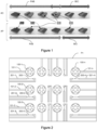
- the platform P1 has a set of nanoprobes (100-1,...100-n) comprising one to nine vertical nanowires (for example four to favor the descent of the cell on the nanoprobe) directly in contact with a conductive access line (101-1,... 101-n).
- This assembly is intended to accommodate cells in culture or for observation.
- Each nano-probe, except for its tip and its conductive access line (101-1%), is covered with an insulating layer (not shown).
- the nanoprobes (100-1,...100-n) are in communication with a perimeter of the platform via a dedicated conductive access line (101-1,...101-n), which is pluggable (connected) electrically to an instrument (also not shown) to generate or detect an electrical signal.
- the platform can thus be used to study neuron-neuron interactions, for example by sending an electrical signal into a neuron of a neural network via one or more nano-probes in electrical contact with this neuron then by detecting the signals electrical signals from another neuron in the network via the nanoprobes in contact with this other neuron.
- the P1 platform includes silicon fin transistors (fin-FET) to detect and measure extracellular ion concentrations (ionic concentration). These fin-FETs (200-1,...200-m) are placed as close as possible to the nanoprobes to measure the resulting ionic concentrations. Each fin-FET is associated with a nano-probe in order to form a pair ⁇ nano-probe, fin-FET ⁇ called nano-sensor.
- the nano-FETs (200-1,...200-m) are in communication with a perimeter of the platform via a dedicated conductive access line (201-1,...201-m), which is connectable ( connected) electrically to an instrument (also not shown) for detecting an electrical signal and more particularly an extracellular ion concentration.
- the nanoprobes can measure the potential propagating (and in particular the speed of its propagation) from one cell to another, as well as the initial electrical potentials and arrival, as well as the ionic concentrations. Only a few sensors are shown in the figure for better readability.
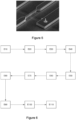
- There figure 4a is a microscopic representation of a four vertical wire nanoprobe of the platform.
- There figure 4b is a microscopic representation of a fin-FET platform.
- There figure 5 is a microscopic representation of a nano-probe with a vertical wire associated with a thin-FET to form a nano-sensor as presented previously.
- the objective is to allow observation of the behavior of groups of cells in growth and/or in culture, without constraining the latter.
- a CN0 neuronal cell (its axons or dendrites being labeled CN0a) is brought into contact with the surface of the P1 platform, which has an array of soma nanoprobes (100-1,... 100-n) comprising a with nine (for example four) vertical nanowires directly in contact with a conductive access line (101-1,...101-n).
- This primary network is called a network of soma nanoprobes because it is intended to receive the somas of the cells, unlike, as explained below, path nanoprobes.
- Each nano-probe, except its tip and the conductive access line is covered with an insulating layer (not shown).
- the soma nanoprobes (100-1,...100-n) are in communication with a perimeter of the platform via a dedicated conductive access line (101-1,...101-n), which is connectable ( connected) electrically to an instrument (also not shown) for generating or detecting an electrical signal.
- the platform can thus be used to study neuron-neuron interactions, for example by sending an electrical signal to a neuron in a neural network via one or several nano-probes in electrical contact with this neuron then detecting the electrical signals of another neuron of the network via the nano-probes in contact with this other neuron.
- the P1 platform includes silicon fin transistors (nano-FETs) for detecting and measuring extracellular ion concentrations (ionic concentration). These nano-FETs (200-1,... 200-m) are arranged as close as possible to the soma nanoprobes to measure the resulting ionic concentrations. Sensors (nanoprobes or nano FETs) are also distributed on the paths to follow the propagation. These paths make it possible to connect the different soma nanoprobes (100-1,... 100-n) to each other to form a network of nanoprobes of somas. The purpose of these pre-established paths (routes), as explained above, is to guide the culture of the cells according to predetermined parameters.
- the objective of this guidance being to constitute a network of cells interconnected, so as to be able to measure potential values and quantity of ion current between these cells when they are positioned (cultivated) on the network of nanoprobes and that the dendrites or axons allow the propagation of electric current from one cell to another.
- the nanoprobes or nano-FETs are positioned along routes (paths) which we know, from the surface specialization of the platform, that they will be the receptacles of the dendrites or axons of the cells during their growth.
- the nano-FETs (200-1,... 200-m) are in communication with a perimeter of the platform via a dedicated conductive access line (201-1,...
- the nanoprobes can measure the potential propagating (and in particular the speed of its propagation) from one cell to another, as well as the initial electrical potentials and arrival as well as the ionic concentrations.
- a path between two soma nanoprobes comprises nano-FETs (300-1,..., 300-l) and/or path nanoprobes (400-1,..., 400-j). These path nanoprobes make it possible to measure the electric potential at different locations of the dendrite or the axon (only two paths are shown in the figure for better readability).
- the nanoprobes and nano-FETs (silicon fin transistors) used in the present technique can be formed from any electrically conductive material, preferably an inorganic material, such as silicon, metal, compound semiconductor, a conductive oxide and a silicide.
- the insulating layer coated on the components of this platform is formed from a material with low cytotoxicity, such as silicon oxide, aluminum oxide and silicon nitride.
- the tips of the nano-probes are either exposed (that is to say free of an insulating coating layer) or coated with an electrically conductive layer, as is explained later in the context of the presentation of the method. manufacturing of said platform, according to a top-down approach.
- the electrically conductive layer is also formed of a material with low cytotoxicity, such as gold, silver and platinum, an alloy of these metals or a conductive organic material (for example pedot:pss).
- a measurement platform based on nanowires is obtained from a 10.16cm (4 inches) silicon-on-insulator (SOI) substrate (4 ⁇ m active Si/1 ⁇ m buried oxide/400 ⁇ m substrate).
- SOI silicon-on-insulator
- a top-down (top-down ) approach is used with a UV photolithography manufacturing process using an i-line stepper followed by RIE plasma etching, to reduce manufacturing costs and facilitate large-scale manufacturing.
- an anti-reflective layer BARC is used under the photoresist.
- this platform manufactured according to the process described above, makes it possible to solve the problem linked to the joint measurement, using the same platform, an electric potential, using at least one nano-probe and extracellular ion concentration with one or more transistors (nano-FET). All of these steps make it possible to obtain a device, or a platform, in a single pass, which is not permitted by the manufacturing methods of the prior art.
- the inventors have implemented an additional step of specialization of the surface of the platform, this additional step making it possible to constrain the culture and the growth of cells at predetermined locations, as presented previously.
- the manufacturing method further comprises a step of chemical functionalization (E110) comprising a photolithography for defining cell attachment patterns and more specifically hydrophilic patterns.
- Hydrophilic zones of larger surfaces are created at the level of the nanoprobes, at the places where it is desired to promote the implantation of soma. Hydrophilic zones are also created in the extension of the nanoprobes, in order to allow cell extensions (axons, dendrites if necessary) to direct the growth of these extensions towards other nanoprobes, on which other somas will be fixed.
- the platform object of the present can be implemented in different ways.
- An advantage of this platform provided by the fact that each nano-device is addressable, is that it allows a localization of the cells deposited (and/or developed) at very precise locations on the platform, which is not permitted by the prior art.
- the use of the platform is not limited to cells of the neuron type, but can be implemented for any type of cell, with a modification of the distance separating the components of the nanoprobes.
- the nanoprobes can be used to measure a potential on the one hand and to transmit an electric impulse to the cells, on the other hand. This pulse transmission can be used to locally open the wall of the stimulated cell, in a precise and reversible manner. Pulse transmission can also be used, under certain conditions, to cause excitation of the cell.
Landscapes
- Health & Medical Sciences (AREA)
- Life Sciences & Earth Sciences (AREA)
- Engineering & Computer Science (AREA)
- Chemical & Material Sciences (AREA)
- Physics & Mathematics (AREA)
- Molecular Biology (AREA)
- Biomedical Technology (AREA)
- General Health & Medical Sciences (AREA)
- Pathology (AREA)
- Immunology (AREA)
- General Physics & Mathematics (AREA)
- Biochemistry (AREA)
- Analytical Chemistry (AREA)
- Biophysics (AREA)
- Nanotechnology (AREA)
- Chemical Kinetics & Catalysis (AREA)
- Microelectronics & Electronic Packaging (AREA)
- Electrochemistry (AREA)
- Hematology (AREA)
- Food Science & Technology (AREA)
- Medicinal Chemistry (AREA)
- Urology & Nephrology (AREA)
- Optics & Photonics (AREA)
- Veterinary Medicine (AREA)
- Public Health (AREA)
- Animal Behavior & Ethology (AREA)
- Surgery (AREA)
- Medical Informatics (AREA)
- Heart & Thoracic Surgery (AREA)
- Spectroscopy & Molecular Physics (AREA)
- Crystallography & Structural Chemistry (AREA)
- Investigating Or Analyzing Materials By The Use Of Electric Means (AREA)
- Apparatus Associated With Microorganisms And Enzymes (AREA)
- Measuring Or Testing Involving Enzymes Or Micro-Organisms (AREA)
- Thin Film Transistor (AREA)
Applications Claiming Priority (2)
| Application Number | Priority Date | Filing Date | Title |
|---|---|---|---|
| FR1761651A FR3074489B1 (fr) | 2017-12-05 | 2017-12-05 | Plateforme de nanostructures pour l’interfacage cellulaire et procede de fabrication correspondant |
| PCT/EP2018/083305 WO2019110485A1 (fr) | 2017-12-05 | 2018-12-03 | Plateforme de nanostructures pour l'interfaçage cellulaire et procede de fabrication correspondant |
Publications (3)
| Publication Number | Publication Date |
|---|---|
| EP3721224A1 EP3721224A1 (fr) | 2020-10-14 |
| EP3721224B1 true EP3721224B1 (fr) | 2023-08-30 |
| EP3721224C0 EP3721224C0 (fr) | 2023-08-30 |
Family
ID=61802066
Family Applications (1)
| Application Number | Title | Priority Date | Filing Date |
|---|---|---|---|
| EP18808036.0A Active EP3721224B1 (fr) | 2017-12-05 | 2018-12-03 | Plateforme de nanostructures pour l'interfaçage cellulaire et procede de fabrication correspondant |
Country Status (5)
| Country | Link |
|---|---|
| US (1) | US12493014B2 (cg-RX-API-DMAC7.html) |
| EP (1) | EP3721224B1 (cg-RX-API-DMAC7.html) |
| JP (1) | JP7266035B2 (cg-RX-API-DMAC7.html) |
| FR (1) | FR3074489B1 (cg-RX-API-DMAC7.html) |
| WO (1) | WO2019110485A1 (cg-RX-API-DMAC7.html) |
Families Citing this family (4)
| Publication number | Priority date | Publication date | Assignee | Title |
|---|---|---|---|---|
| FR3074489B1 (fr) * | 2017-12-05 | 2023-04-21 | Centre Nat Rech Scient | Plateforme de nanostructures pour l’interfacage cellulaire et procede de fabrication correspondant |
| DE102020122823B4 (de) * | 2020-05-12 | 2022-06-02 | Taiwan Semiconductor Manufacturing Co., Ltd. | Halbleitervorrichtungen mit entkopplungskondensatoren |
| EP4256327B1 (fr) | 2020-12-04 | 2026-02-11 | Centre National de la Recherche Scientifique (CNRS) | Plateforme de nanostructures pour l'interfaçage cellulaire et procédé de fabrication correspondant |
| FR3117102B1 (fr) | 2020-12-04 | 2023-01-06 | Centre Nat Rech Scient | Plateforme de nanostructures pour l’interfaçage cellulaire et procédé de fabrication correspondant |
Family Cites Families (36)
| Publication number | Priority date | Publication date | Assignee | Title |
|---|---|---|---|---|
| US5923421A (en) * | 1997-07-24 | 1999-07-13 | Lockheed Martin Energy Research Corporation | Chemical detection using calorimetric spectroscopy |
| US20040248075A1 (en) * | 2001-10-10 | 2004-12-09 | Koushi Yamaguchi | Photocatalytic material that selectively inactivating biologically harmful substance and utilization thereof |
| JP2007501525A (ja) * | 2003-08-04 | 2007-01-25 | ナノシス・インコーポレイテッド | ナノワイヤ複合体およびこれらに由来する電子基板を作製するためのシステムおよび方法 |
| US7741618B2 (en) * | 2004-11-19 | 2010-06-22 | Science & Engineering Services, Inc. | Enhanced portable digital lidar system |
| US7544978B2 (en) * | 2005-01-24 | 2009-06-09 | Lawrence Livermore National Security, Llc | Lipid nanotube or nanowire sensor |
| EP1902143A1 (en) * | 2005-03-29 | 2008-03-26 | Applera Corporation | Nanowire-based system for analysis of nucleic acids |
| EP2013611A2 (en) * | 2006-03-15 | 2009-01-14 | The President and Fellows of Harvard College | Nanobioelectronics |
| US7388200B2 (en) * | 2006-10-19 | 2008-06-17 | Hewlett-Packard Development Company, L.P. | Sensing method and nanosensing device for performing the same |
| US20080128760A1 (en) * | 2006-12-04 | 2008-06-05 | Electronics And Telecommunications Research Institute | Schottky barrier nanowire field effect transistor and method for fabricating the same |
| US9188594B2 (en) * | 2006-12-06 | 2015-11-17 | Yale University | Nanoelectronic-enzyme linked immunosorbent assay system and method |
| US7608854B2 (en) * | 2007-01-29 | 2009-10-27 | Hewlett-Packard Development Company, L.P. | Electronic device and method of making the same |
| US7905013B2 (en) | 2007-06-04 | 2011-03-15 | Sharp Laboratories Of America, Inc. | Method for forming an iridium oxide (IrOx) nanowire neural sensor array |
| US7709298B2 (en) * | 2007-07-18 | 2010-05-04 | Hewlett-Packard Development Company, L.P. | Selectively altering a predetermined portion or an external member in contact with the predetermined portion |
| KR100987385B1 (ko) * | 2007-09-03 | 2010-10-12 | 금오공과대학교 산학협력단 | 나노 구조물 복합체 및 그의 제조 방법 |
| US9377399B2 (en) * | 2008-03-18 | 2016-06-28 | Lawrence Livermore National Security, Llc | Resonant optical transducers for in-situ gas detection |
| FR2930073B1 (fr) | 2008-04-11 | 2010-09-03 | Centre Nat Rech Scient | Procede de fabrication de transistors mosfet complementaires de type p et n, et dispositif electronique comprenant de tels transistors, et processeur comprenant au moins un tel dispositif. |
| US8169006B2 (en) * | 2008-11-29 | 2012-05-01 | Electronics And Telecommunications Research Institute | Bio-sensor chip for detecting target material |
| US20100216256A1 (en) * | 2009-02-17 | 2010-08-26 | Florida State University Research Foundation | Nanobelt-based sensors and detection methods |
| KR101138011B1 (ko) * | 2009-08-05 | 2012-04-20 | 전북대학교산학협력단 | 자극?감지 일체형 바이오-메드 칩 및 그 제조방법 |
| US9880126B2 (en) * | 2010-09-24 | 2018-01-30 | Ajou University Industry-Academic Cooperation Foundation | Biosensor based on carbon nanotube-electric field effect transistor and method for producing the same |
| FR2968125B1 (fr) * | 2010-11-26 | 2013-11-29 | Centre Nat Rech Scient | Procédé de fabrication d'un dispositif de transistor a effet de champ implémenté sur un réseau de nanofils verticaux, dispositif de transistor résultant, dispositif électronique comprenant de tels dispositifs de transistors, et processeur comprenant au moins un tel dispositif électronique |
| US9157888B2 (en) * | 2011-05-05 | 2015-10-13 | Graphensic Ab | Field effect transistor for chemical sensing using graphene, chemical sensor using the transistor and method for producing the transistor |
| US8860137B2 (en) * | 2011-06-08 | 2014-10-14 | University Of Southern California | Radio frequency devices based on carbon nanomaterials |
| EP2802859A1 (en) * | 2012-01-10 | 2014-11-19 | Northeastern University | Wireless swnt sensor integrated with microfluidic system for various liquid sensing applications |
| US10390724B2 (en) * | 2013-06-26 | 2019-08-27 | The Penn State Research Foundation | Three-dimensional bio-medical probe sensing and contacting structures with addressibility and tunability |
| TWI634331B (zh) * | 2014-06-25 | 2018-09-01 | Dcg Systems, Inc. | 電子裝置的奈米探測系統及其奈米探針 |
| EP3705881A1 (en) * | 2014-10-24 | 2020-09-09 | Abbott Laboratories | Paper substrate diagnostic apparatus and related methods and systems |
| US10006910B2 (en) * | 2014-12-18 | 2018-06-26 | Agilome, Inc. | Chemically-sensitive field effect transistors, systems, and methods for manufacturing and using the same |
| US9859394B2 (en) * | 2014-12-18 | 2018-01-02 | Agilome, Inc. | Graphene FET devices, systems, and methods of using the same for sequencing nucleic acids |
| US10020300B2 (en) * | 2014-12-18 | 2018-07-10 | Agilome, Inc. | Graphene FET devices, systems, and methods of using the same for sequencing nucleic acids |
| WO2017098518A1 (en) * | 2015-12-09 | 2017-06-15 | Ramot At Tel-Aviv University Ltd. | Method and system for sensing |
| JP7109785B2 (ja) * | 2016-01-14 | 2022-08-01 | ロズウェル バイオテクノロジーズ,インコーポレイテッド | 分子センサーおよび関連方法 |
| WO2017127551A1 (en) | 2016-01-19 | 2017-07-27 | The Regents Of The University Of California | Addressable vertical nanowire probe arrays and fabrication methods |
| EP3408220A4 (en) * | 2016-01-28 | 2019-09-04 | Roswell Biotechnologies, Inc | METHOD AND DEVICE FOR MEASURING ANALYTES USING LARGE CALCULAR MOLECULAR ELECTRONIC SENSOR ARRAYS |
| WO2017209821A2 (en) * | 2016-03-11 | 2017-12-07 | The Johns Hopkins University | Non-optical label-free biomolecular detection at electrially displaced liquid interfaces using interfacial electrokinetic transduction (iet) |
| FR3074489B1 (fr) * | 2017-12-05 | 2023-04-21 | Centre Nat Rech Scient | Plateforme de nanostructures pour l’interfacage cellulaire et procede de fabrication correspondant |
-
2017
- 2017-12-05 FR FR1761651A patent/FR3074489B1/fr active Active
-
2018
- 2018-12-03 US US16/769,927 patent/US12493014B2/en active Active
- 2018-12-03 EP EP18808036.0A patent/EP3721224B1/fr active Active
- 2018-12-03 WO PCT/EP2018/083305 patent/WO2019110485A1/fr not_active Ceased
- 2018-12-03 JP JP2020531128A patent/JP7266035B2/ja active Active
Also Published As
| Publication number | Publication date |
|---|---|
| FR3074489B1 (fr) | 2023-04-21 |
| EP3721224C0 (fr) | 2023-08-30 |
| US12493014B2 (en) | 2025-12-09 |
| WO2019110485A1 (fr) | 2019-06-13 |
| EP3721224A1 (fr) | 2020-10-14 |
| US20200386710A1 (en) | 2020-12-10 |
| JP2021505163A (ja) | 2021-02-18 |
| JP7266035B2 (ja) | 2023-04-27 |
| FR3074489A1 (fr) | 2019-06-07 |
Similar Documents
| Publication | Publication Date | Title |
|---|---|---|
| WO2019110485A1 (fr) | Plateforme de nanostructures pour l'interfaçage cellulaire et procede de fabrication correspondant | |
| Li et al. | Advances in nanowire transistor‐based biosensors | |
| US9595685B2 (en) | Nanoscale wires, nanoscale wire FET devices, and nanotube-electronic hybrid devices for sensing and other applications | |
| US9551698B2 (en) | Microneedle | |
| DK2621584T3 (en) | NANO WIRE TO electrophysiological APPLICATIONS | |
| US20170296806A1 (en) | Nanopillar electrode devices and methods of recording action potentials | |
| US20040004182A1 (en) | Sample for simultaneously conducting electro-chemical and topographic near-field microscopy | |
| JP2009156572A (ja) | イオンチャンネルタンパク質バイオセンサー | |
| US12157666B2 (en) | Sharp, vertically aligned nanowire electrode arrays, high-yield fabrication and intracellular recording | |
| US20160252506A1 (en) | Silicon nanowire-based sensor arrays | |
| Zhang et al. | Probing electrical signals in the retina via graphene-integrated microfluidic platforms | |
| US20050017173A1 (en) | Individually addressable nanoelectrode array | |
| CN107210319B (zh) | 大规模低成本纳米传感器、纳米针和纳米泵阵列 | |
| EP4256327B1 (fr) | Plateforme de nanostructures pour l'interfaçage cellulaire et procédé de fabrication correspondant | |
| FR3117101A1 (fr) | Plateforme de nanostructures pour l’interfaçage cellulaire et procédé de fabrication correspondant | |
| Shandhi et al. | Reusable high aspect ratio 3-D nickel shadow mask | |
| KR20210044615A (ko) | 레이저 패터닝과 감광성 폴리머 절연막을 이용한 평면형 다중 전극 어레이 제조 방법 | |
| Meyburg et al. | Advanced CMOS process for floating gate field-effect transistors in bioelectronic applications | |
| Shokoohimehr | Nanostraw-Nanocavity MEAs as a new tool for long-term and high sensitive recording of neuronal signals | |
| Yousefi | Nanoscale Approaches for Optical and Electrochemical Biomolecular Recognition | |
| Woodhams | Graphene Microelectrode Arrays to Combine Electrophysiology with Fluorescence Imaging of Amyloid Proteins | |
| Wu et al. | In-plane fabrication of insulated gold-tip probes for electrochemical and force spectroscopy molecular experiments | |
| Nguyen | Neuroprobe: Design, fabrication, and in vitro characterization of combined electrochemical and potential microelectrodes | |
| Pisano et al. | Development of an uncooled photomechanic infrared sensor based on the IR organ of the pyrophilous jewel beetle Melanophila acuminata | |
| FR2986802A1 (fr) | Dispositif et procede de manipulation et traitement de cellules par champ electrique. |
Legal Events
| Date | Code | Title | Description |
|---|---|---|---|
| STAA | Information on the status of an ep patent application or granted ep patent |
Free format text: STATUS: UNKNOWN |
|
| STAA | Information on the status of an ep patent application or granted ep patent |
Free format text: STATUS: THE INTERNATIONAL PUBLICATION HAS BEEN MADE |
|
| PUAI | Public reference made under article 153(3) epc to a published international application that has entered the european phase |
Free format text: ORIGINAL CODE: 0009012 |
|
| STAA | Information on the status of an ep patent application or granted ep patent |
Free format text: STATUS: REQUEST FOR EXAMINATION WAS MADE |
|
| 17P | Request for examination filed |
Effective date: 20200520 |
|
| AK | Designated contracting states |
Kind code of ref document: A1 Designated state(s): AL AT BE BG CH CY CZ DE DK EE ES FI FR GB GR HR HU IE IS IT LI LT LU LV MC MK MT NL NO PL PT RO RS SE SI SK SM TR |
|
| AX | Request for extension of the european patent |
Extension state: BA ME |
|
| DAV | Request for validation of the european patent (deleted) | ||
| DAX | Request for extension of the european patent (deleted) | ||
| STAA | Information on the status of an ep patent application or granted ep patent |
Free format text: STATUS: EXAMINATION IS IN PROGRESS |
|
| 17Q | First examination report despatched |
Effective date: 20220715 |
|
| GRAP | Despatch of communication of intention to grant a patent |
Free format text: ORIGINAL CODE: EPIDOSNIGR1 |
|
| STAA | Information on the status of an ep patent application or granted ep patent |
Free format text: STATUS: GRANT OF PATENT IS INTENDED |
|
| INTG | Intention to grant announced |
Effective date: 20230324 |
|
| GRAS | Grant fee paid |
Free format text: ORIGINAL CODE: EPIDOSNIGR3 |
|
| GRAA | (expected) grant |
Free format text: ORIGINAL CODE: 0009210 |
|
| STAA | Information on the status of an ep patent application or granted ep patent |
Free format text: STATUS: THE PATENT HAS BEEN GRANTED |
|
| AK | Designated contracting states |
Kind code of ref document: B1 Designated state(s): AL AT BE BG CH CY CZ DE DK EE ES FI FR GB GR HR HU IE IS IT LI LT LU LV MC MK MT NL NO PL PT RO RS SE SI SK SM TR |
|
| REG | Reference to a national code |
Ref country code: GB Ref legal event code: FG4D Free format text: NOT ENGLISH |
|
| REG | Reference to a national code |
Ref country code: CH Ref legal event code: EP |
|
| REG | Reference to a national code |
Ref country code: DE Ref legal event code: R096 Ref document number: 602018056544 Country of ref document: DE |
|
| REG | Reference to a national code |
Ref country code: IE Ref legal event code: FG4D Free format text: LANGUAGE OF EP DOCUMENT: FRENCH |
|
| U01 | Request for unitary effect filed |
Effective date: 20230908 |
|
| U07 | Unitary effect registered |
Designated state(s): AT BE BG DE DK EE FI FR IT LT LU LV MT NL PT SE SI Effective date: 20230914 |
|
| PG25 | Lapsed in a contracting state [announced via postgrant information from national office to epo] |
Ref country code: GR Free format text: LAPSE BECAUSE OF FAILURE TO SUBMIT A TRANSLATION OF THE DESCRIPTION OR TO PAY THE FEE WITHIN THE PRESCRIBED TIME-LIMIT Effective date: 20231201 |
|
| PG25 | Lapsed in a contracting state [announced via postgrant information from national office to epo] |
Ref country code: IS Free format text: LAPSE BECAUSE OF FAILURE TO SUBMIT A TRANSLATION OF THE DESCRIPTION OR TO PAY THE FEE WITHIN THE PRESCRIBED TIME-LIMIT Effective date: 20231230 |
|
| U20 | Renewal fee for the european patent with unitary effect paid |
Year of fee payment: 6 Effective date: 20231219 |
|
| PG25 | Lapsed in a contracting state [announced via postgrant information from national office to epo] |
Ref country code: RS Free format text: LAPSE BECAUSE OF FAILURE TO SUBMIT A TRANSLATION OF THE DESCRIPTION OR TO PAY THE FEE WITHIN THE PRESCRIBED TIME-LIMIT Effective date: 20230830 Ref country code: NO Free format text: LAPSE BECAUSE OF FAILURE TO SUBMIT A TRANSLATION OF THE DESCRIPTION OR TO PAY THE FEE WITHIN THE PRESCRIBED TIME-LIMIT Effective date: 20231130 Ref country code: IS Free format text: LAPSE BECAUSE OF FAILURE TO SUBMIT A TRANSLATION OF THE DESCRIPTION OR TO PAY THE FEE WITHIN THE PRESCRIBED TIME-LIMIT Effective date: 20231230 Ref country code: HR Free format text: LAPSE BECAUSE OF FAILURE TO SUBMIT A TRANSLATION OF THE DESCRIPTION OR TO PAY THE FEE WITHIN THE PRESCRIBED TIME-LIMIT Effective date: 20230830 Ref country code: GR Free format text: LAPSE BECAUSE OF FAILURE TO SUBMIT A TRANSLATION OF THE DESCRIPTION OR TO PAY THE FEE WITHIN THE PRESCRIBED TIME-LIMIT Effective date: 20231201 |
|
| PG25 | Lapsed in a contracting state [announced via postgrant information from national office to epo] |
Ref country code: PL Free format text: LAPSE BECAUSE OF FAILURE TO SUBMIT A TRANSLATION OF THE DESCRIPTION OR TO PAY THE FEE WITHIN THE PRESCRIBED TIME-LIMIT Effective date: 20230830 |
|
| PG25 | Lapsed in a contracting state [announced via postgrant information from national office to epo] |
Ref country code: ES Free format text: LAPSE BECAUSE OF FAILURE TO SUBMIT A TRANSLATION OF THE DESCRIPTION OR TO PAY THE FEE WITHIN THE PRESCRIBED TIME-LIMIT Effective date: 20230830 |
|
| PG25 | Lapsed in a contracting state [announced via postgrant information from national office to epo] |
Ref country code: SM Free format text: LAPSE BECAUSE OF FAILURE TO SUBMIT A TRANSLATION OF THE DESCRIPTION OR TO PAY THE FEE WITHIN THE PRESCRIBED TIME-LIMIT Effective date: 20230830 Ref country code: RO Free format text: LAPSE BECAUSE OF FAILURE TO SUBMIT A TRANSLATION OF THE DESCRIPTION OR TO PAY THE FEE WITHIN THE PRESCRIBED TIME-LIMIT Effective date: 20230830 Ref country code: ES Free format text: LAPSE BECAUSE OF FAILURE TO SUBMIT A TRANSLATION OF THE DESCRIPTION OR TO PAY THE FEE WITHIN THE PRESCRIBED TIME-LIMIT Effective date: 20230830 Ref country code: CZ Free format text: LAPSE BECAUSE OF FAILURE TO SUBMIT A TRANSLATION OF THE DESCRIPTION OR TO PAY THE FEE WITHIN THE PRESCRIBED TIME-LIMIT Effective date: 20230830 Ref country code: SK Free format text: LAPSE BECAUSE OF FAILURE TO SUBMIT A TRANSLATION OF THE DESCRIPTION OR TO PAY THE FEE WITHIN THE PRESCRIBED TIME-LIMIT Effective date: 20230830 |
|
| REG | Reference to a national code |
Ref country code: DE Ref legal event code: R097 Ref document number: 602018056544 Country of ref document: DE |
|
| PLBE | No opposition filed within time limit |
Free format text: ORIGINAL CODE: 0009261 |
|
| STAA | Information on the status of an ep patent application or granted ep patent |
Free format text: STATUS: NO OPPOSITION FILED WITHIN TIME LIMIT |
|
| 26N | No opposition filed |
Effective date: 20240603 |
|
| PG25 | Lapsed in a contracting state [announced via postgrant information from national office to epo] |
Ref country code: MC Free format text: LAPSE BECAUSE OF FAILURE TO SUBMIT A TRANSLATION OF THE DESCRIPTION OR TO PAY THE FEE WITHIN THE PRESCRIBED TIME-LIMIT Effective date: 20230830 |
|
| PG25 | Lapsed in a contracting state [announced via postgrant information from national office to epo] |
Ref country code: MC Free format text: LAPSE BECAUSE OF FAILURE TO SUBMIT A TRANSLATION OF THE DESCRIPTION OR TO PAY THE FEE WITHIN THE PRESCRIBED TIME-LIMIT Effective date: 20230830 |
|
| REG | Reference to a national code |
Ref country code: IE Ref legal event code: MM4A |
|
| PG25 | Lapsed in a contracting state [announced via postgrant information from national office to epo] |
Ref country code: IE Free format text: LAPSE BECAUSE OF NON-PAYMENT OF DUE FEES Effective date: 20231203 |
|
| PG25 | Lapsed in a contracting state [announced via postgrant information from national office to epo] |
Ref country code: IE Free format text: LAPSE BECAUSE OF NON-PAYMENT OF DUE FEES Effective date: 20231203 |
|
| U20 | Renewal fee for the european patent with unitary effect paid |
Year of fee payment: 7 Effective date: 20241217 |
|
| PG25 | Lapsed in a contracting state [announced via postgrant information from national office to epo] |
Ref country code: CY Free format text: LAPSE BECAUSE OF FAILURE TO SUBMIT A TRANSLATION OF THE DESCRIPTION OR TO PAY THE FEE WITHIN THE PRESCRIBED TIME-LIMIT; INVALID AB INITIO Effective date: 20181203 |
|
| PG25 | Lapsed in a contracting state [announced via postgrant information from national office to epo] |
Ref country code: HU Free format text: LAPSE BECAUSE OF FAILURE TO SUBMIT A TRANSLATION OF THE DESCRIPTION OR TO PAY THE FEE WITHIN THE PRESCRIBED TIME-LIMIT; INVALID AB INITIO Effective date: 20181203 |
|
| PG25 | Lapsed in a contracting state [announced via postgrant information from national office to epo] |
Ref country code: TR Free format text: LAPSE BECAUSE OF FAILURE TO SUBMIT A TRANSLATION OF THE DESCRIPTION OR TO PAY THE FEE WITHIN THE PRESCRIBED TIME-LIMIT Effective date: 20230830 |
|
| REG | Reference to a national code |
Ref country code: CH Ref legal event code: U11 Free format text: ST27 STATUS EVENT CODE: U-0-0-U10-U11 (AS PROVIDED BY THE NATIONAL OFFICE) Effective date: 20260105 |
|
| PGFP | Annual fee paid to national office [announced via postgrant information from national office to epo] |
Ref country code: GB Payment date: 20251223 Year of fee payment: 8 |
|
| U20 | Renewal fee for the european patent with unitary effect paid |
Year of fee payment: 8 Effective date: 20251218 |
|
| REG | Reference to a national code |
Ref country code: CH Ref legal event code: R17 Free format text: ST27 STATUS EVENT CODE: U-0-0-R10-R17 (AS PROVIDED BY THE NATIONAL OFFICE) Effective date: 20260211 |
|
| PGFP | Annual fee paid to national office [announced via postgrant information from national office to epo] |
Ref country code: CH Payment date: 20260105 Year of fee payment: 8 |