EP3720258A1 - Glass core, multilayer wiring substrate, and method for manufacturing glass core - Google Patents
Glass core, multilayer wiring substrate, and method for manufacturing glass core Download PDFInfo
- Publication number
- EP3720258A1 EP3720258A1 EP18883284.4A EP18883284A EP3720258A1 EP 3720258 A1 EP3720258 A1 EP 3720258A1 EP 18883284 A EP18883284 A EP 18883284A EP 3720258 A1 EP3720258 A1 EP 3720258A1
- Authority
- EP
- European Patent Office
- Prior art keywords
- layer
- plating layer
- glass
- electroless nickel
- nickel plating
- Prior art date
- Legal status (The legal status is an assumption and is not a legal conclusion. Google has not performed a legal analysis and makes no representation as to the accuracy of the status listed.)
- Granted
Links
Images






Classifications
-
- H—ELECTRICITY
- H05—ELECTRIC TECHNIQUES NOT OTHERWISE PROVIDED FOR
- H05K—PRINTED CIRCUITS; CASINGS OR CONSTRUCTIONAL DETAILS OF ELECTRIC APPARATUS; MANUFACTURE OF ASSEMBLAGES OF ELECTRICAL COMPONENTS
- H05K3/00—Apparatus or processes for manufacturing printed circuits
- H05K3/46—Manufacturing multilayer circuits
- H05K3/4602—Manufacturing multilayer circuits characterized by a special circuit board as base or central core whereon additional circuit layers are built or additional circuit boards are laminated
- H05K3/4605—Manufacturing multilayer circuits characterized by a special circuit board as base or central core whereon additional circuit layers are built or additional circuit boards are laminated made from inorganic insulating material
-
- H—ELECTRICITY
- H05—ELECTRIC TECHNIQUES NOT OTHERWISE PROVIDED FOR
- H05K—PRINTED CIRCUITS; CASINGS OR CONSTRUCTIONAL DETAILS OF ELECTRIC APPARATUS; MANUFACTURE OF ASSEMBLAGES OF ELECTRICAL COMPONENTS
- H05K1/00—Printed circuits
- H05K1/02—Details
- H05K1/03—Use of materials for the substrate
- H05K1/0306—Inorganic insulating substrates, e.g. ceramic, glass
-
- H—ELECTRICITY
- H05—ELECTRIC TECHNIQUES NOT OTHERWISE PROVIDED FOR
- H05K—PRINTED CIRCUITS; CASINGS OR CONSTRUCTIONAL DETAILS OF ELECTRIC APPARATUS; MANUFACTURE OF ASSEMBLAGES OF ELECTRICAL COMPONENTS
- H05K1/00—Printed circuits
- H05K1/02—Details
- H05K1/11—Printed elements for providing electric connections to or between printed circuits
-
- H—ELECTRICITY
- H05—ELECTRIC TECHNIQUES NOT OTHERWISE PROVIDED FOR
- H05K—PRINTED CIRCUITS; CASINGS OR CONSTRUCTIONAL DETAILS OF ELECTRIC APPARATUS; MANUFACTURE OF ASSEMBLAGES OF ELECTRICAL COMPONENTS
- H05K1/00—Printed circuits
- H05K1/16—Printed circuits incorporating printed electric components, e.g. printed resistors, capacitors or inductors
- H05K1/162—Printed circuits incorporating printed electric components, e.g. printed resistors, capacitors or inductors incorporating printed capacitors
-
- H—ELECTRICITY
- H05—ELECTRIC TECHNIQUES NOT OTHERWISE PROVIDED FOR
- H05K—PRINTED CIRCUITS; CASINGS OR CONSTRUCTIONAL DETAILS OF ELECTRIC APPARATUS; MANUFACTURE OF ASSEMBLAGES OF ELECTRICAL COMPONENTS
- H05K3/00—Apparatus or processes for manufacturing printed circuits
- H05K3/46—Manufacturing multilayer circuits
-
- H—ELECTRICITY
- H05—ELECTRIC TECHNIQUES NOT OTHERWISE PROVIDED FOR
- H05K—PRINTED CIRCUITS; CASINGS OR CONSTRUCTIONAL DETAILS OF ELECTRIC APPARATUS; MANUFACTURE OF ASSEMBLAGES OF ELECTRICAL COMPONENTS
- H05K1/00—Printed circuits
- H05K1/02—Details
- H05K1/11—Printed elements for providing electric connections to or between printed circuits
- H05K1/115—Via connections; Lands around holes or via connections
- H05K1/116—Lands, clearance holes or other lay-out details concerning the surrounding of a via
-
- H—ELECTRICITY
- H05—ELECTRIC TECHNIQUES NOT OTHERWISE PROVIDED FOR
- H05K—PRINTED CIRCUITS; CASINGS OR CONSTRUCTIONAL DETAILS OF ELECTRIC APPARATUS; MANUFACTURE OF ASSEMBLAGES OF ELECTRICAL COMPONENTS
- H05K1/00—Printed circuits
- H05K1/18—Printed circuits structurally associated with non-printed electric components
-
- H—ELECTRICITY
- H05—ELECTRIC TECHNIQUES NOT OTHERWISE PROVIDED FOR
- H05K—PRINTED CIRCUITS; CASINGS OR CONSTRUCTIONAL DETAILS OF ELECTRIC APPARATUS; MANUFACTURE OF ASSEMBLAGES OF ELECTRICAL COMPONENTS
- H05K3/00—Apparatus or processes for manufacturing printed circuits
- H05K3/10—Apparatus or processes for manufacturing printed circuits in which conductive material is applied to the insulating support in such a manner as to form the desired conductive pattern
- H05K3/108—Apparatus or processes for manufacturing printed circuits in which conductive material is applied to the insulating support in such a manner as to form the desired conductive pattern by semi-additive methods; masks therefor
-
- H—ELECTRICITY
- H05—ELECTRIC TECHNIQUES NOT OTHERWISE PROVIDED FOR
- H05K—PRINTED CIRCUITS; CASINGS OR CONSTRUCTIONAL DETAILS OF ELECTRIC APPARATUS; MANUFACTURE OF ASSEMBLAGES OF ELECTRICAL COMPONENTS
- H05K3/00—Apparatus or processes for manufacturing printed circuits
- H05K3/38—Improvement of the adhesion between the insulating substrate and the metal
- H05K3/388—Improvement of the adhesion between the insulating substrate and the metal by the use of a metallic or inorganic thin film adhesion layer
-
- H—ELECTRICITY
- H05—ELECTRIC TECHNIQUES NOT OTHERWISE PROVIDED FOR
- H05K—PRINTED CIRCUITS; CASINGS OR CONSTRUCTIONAL DETAILS OF ELECTRIC APPARATUS; MANUFACTURE OF ASSEMBLAGES OF ELECTRICAL COMPONENTS
- H05K3/00—Apparatus or processes for manufacturing printed circuits
- H05K3/40—Forming printed elements for providing electric connections to or between printed circuits
- H05K3/42—Plated through-holes or plated via connections
- H05K3/422—Plated through-holes or plated via connections characterised by electroless plating method; pretreatment therefor
-
- H—ELECTRICITY
- H05—ELECTRIC TECHNIQUES NOT OTHERWISE PROVIDED FOR
- H05K—PRINTED CIRCUITS; CASINGS OR CONSTRUCTIONAL DETAILS OF ELECTRIC APPARATUS; MANUFACTURE OF ASSEMBLAGES OF ELECTRICAL COMPONENTS
- H05K3/00—Apparatus or processes for manufacturing printed circuits
- H05K3/46—Manufacturing multilayer circuits
- H05K3/4644—Manufacturing multilayer circuits by building the multilayer layer by layer, i.e. build-up multilayer circuits
-
- H—ELECTRICITY
- H10—SEMICONDUCTOR DEVICES; ELECTRIC SOLID-STATE DEVICES NOT OTHERWISE PROVIDED FOR
- H10W—GENERIC PACKAGES, INTERCONNECTIONS, CONNECTORS OR OTHER CONSTRUCTIONAL DETAILS OF DEVICES COVERED BY CLASS H10
- H10W70/00—Package substrates; Interposers; Redistribution layers [RDL]
- H10W70/60—Insulating or insulated package substrates; Interposers; Redistribution layers
- H10W70/62—Insulating or insulated package substrates; Interposers; Redistribution layers characterised by their interconnections
- H10W70/63—Vias, e.g. via plugs
- H10W70/635—Through-vias
-
- H—ELECTRICITY
- H10—SEMICONDUCTOR DEVICES; ELECTRIC SOLID-STATE DEVICES NOT OTHERWISE PROVIDED FOR
- H10W—GENERIC PACKAGES, INTERCONNECTIONS, CONNECTORS OR OTHER CONSTRUCTIONAL DETAILS OF DEVICES COVERED BY CLASS H10
- H10W70/00—Package substrates; Interposers; Redistribution layers [RDL]
- H10W70/60—Insulating or insulated package substrates; Interposers; Redistribution layers
- H10W70/67—Insulating or insulated package substrates; Interposers; Redistribution layers characterised by their insulating layers or insulating parts
- H10W70/68—Shapes or dispositions thereof
- H10W70/685—Shapes or dispositions thereof comprising multiple insulating layers
-
- H—ELECTRICITY
- H10—SEMICONDUCTOR DEVICES; ELECTRIC SOLID-STATE DEVICES NOT OTHERWISE PROVIDED FOR
- H10W—GENERIC PACKAGES, INTERCONNECTIONS, CONNECTORS OR OTHER CONSTRUCTIONAL DETAILS OF DEVICES COVERED BY CLASS H10
- H10W70/00—Package substrates; Interposers; Redistribution layers [RDL]
- H10W70/60—Insulating or insulated package substrates; Interposers; Redistribution layers
- H10W70/67—Insulating or insulated package substrates; Interposers; Redistribution layers characterised by their insulating layers or insulating parts
- H10W70/69—Insulating materials thereof
-
- H—ELECTRICITY
- H10—SEMICONDUCTOR DEVICES; ELECTRIC SOLID-STATE DEVICES NOT OTHERWISE PROVIDED FOR
- H10W—GENERIC PACKAGES, INTERCONNECTIONS, CONNECTORS OR OTHER CONSTRUCTIONAL DETAILS OF DEVICES COVERED BY CLASS H10
- H10W70/00—Package substrates; Interposers; Redistribution layers [RDL]
- H10W70/60—Insulating or insulated package substrates; Interposers; Redistribution layers
- H10W70/67—Insulating or insulated package substrates; Interposers; Redistribution layers characterised by their insulating layers or insulating parts
- H10W70/69—Insulating materials thereof
- H10W70/692—Ceramics or glasses
-
- H—ELECTRICITY
- H10—SEMICONDUCTOR DEVICES; ELECTRIC SOLID-STATE DEVICES NOT OTHERWISE PROVIDED FOR
- H10W—GENERIC PACKAGES, INTERCONNECTIONS, CONNECTORS OR OTHER CONSTRUCTIONAL DETAILS OF DEVICES COVERED BY CLASS H10
- H10W72/00—Interconnections or connectors in packages
- H10W72/20—Bump connectors, e.g. solder bumps or copper pillars; Dummy bumps; Thermal bumps
Definitions
- the present invention relates to a glass core, a multilayer circuit board, and a method of manufacturing a glass core.
- a glass epoxy resin is used as a core material included in the circuit board.
- a circuit board including a glass plate as a core material has attracted attention.
- a glass plate can achieve a higher degree of smoothness than a core material made of a glass epoxy resin.
- ultrafine wires can be formed on a circuit board including a glass plate, and, thus, high-density implementation is possible by using a circuit board including a glass plate.
- the coefficient of linear thermal expansion (CTE) of a glass plate within the temperature range of 20°C or more and 260°C or less, almost coincides with the coefficient of linear thermal expansion of a semiconductor chip made of a silicon substrate within the temperature range of 20°C or more and 260°C or less.
- a circuit board including a glass plate allows implementation with reduced residual stress. Furthermore, a circuit board including a glass plate is advantageous in that it is excellent for high-speed communication. From the foregoing points, a circuit board including a glass plate has been attracting attention as a wiring substrate of semiconductor modules to be mounted in high-performance electronic devices.
- NPL 1 Takagi, Kiyoshi, Yokuwakaru purinto haisenban no dekirumade (Easy to Understand Manufacturing Processes for Printed Circuit Boards), 2nd Edition, April 2008, pp.201-202, Nikkan Kogyo Shimbun, Ltd.
- a circuit board or a portion of a circuit board is formed by forming wires on a glass plate. This is referred to as a glass core.
- a semi-additive process is applied (NPL 1).
- NPL 1 a semi-additive process
- Such a process can be applied to provide an insulating resin layer after a conduction layer has been formed on a glass plate, and stack a conductor on the insulating resin layer, to form multiple layers of wires.
- a dielectric layer is provided on a glass plate, it is difficult to apply a conventional semi-additive process. The reason for this will be described.
- a process of providing a seed layer on a glass plate providing an electrolytic copper plating layer on the seed layer, etching unnecessary parts of the seed layer, providing a dielectric layer on the electrolytic copper plating layer, and further providing another electrolytic copper plating layer on the dielectric layer.
- a dielectric layer can be provided without an insulating resin layer.
- an undercut in the electrolytic copper plating layer formed on the glass plate via the seed layer formed when unnecessary parts of the seed layer is etched causes a new issue in that the electrolytic copper plating layer cannot be formed on the dielectric layer.
- another process may be considered in which a metal layer formed by sputtering and a seed layer including an electroless nickel plating layer are formed on a glass plate, an electrolytic copper plating layer is formed on the electroless nickel plating layer, a dielectric layer is formed on the electrolytic copper plating layer on the glass plate, and another electrolytic copper plating layer is formed on the dielectric layer.
- a metal layer formed by sputtering and a seed layer including an electroless nickel plating layer are formed on a glass plate
- an electrolytic copper plating layer is formed on the electroless nickel plating layer
- a dielectric layer is formed on the electrolytic copper plating layer on the glass plate
- another electrolytic copper plating layer is formed on the dielectric layer.
- an alkaline etching agent should be used for etching of unnecessary parts of the electroless nickel plating layer.
- an alkaline etching agent is used, there are cases in which a defect in the formation of the electrolytic copper plating layer on the dielectric layer occurs due to an undercut in the electrolytic copper plating layer formed on the glass plate via the glass plate.
- the present invention which has been conceived in view of the above-described issue, provides a glass core, a multilayer circuit board, and a method of manufacturing a glass core that enables appropriate formation of copper wiring and suppresses cracking and the like.
- a glass core includes a glass plate; a first metal layer disposed on the glass plate; a first electrolytic copper plating layer disposed on the first metal layer; a dielectric layer disposed above the first electrolytic copper plating layer; a second metal layer disposed on the dielectric layer; an electroless nickel plating layer disposed on the second metal layer and having a phosphorus content of less than 5 mass%; and a second electrolytic copper plating layer disposed on the electroless nickel plating layer.
- a method of manufacturing a glass core includes forming a first metal layer on a glass plate; forming a first electrolytic copper plating layer above the first metal layer; forming a dielectric layer on the first electrolytic copper plating layer; forming a second metal layer on the dielectric layer; forming an electroless nickel plating layer disposed on the second metal layer and having a phosphorus content of less than 5 mass%; forming a second electrolytic copper plating layer disposed on the electroless nickel plating layer; and removing unnecessary parts of the electroless nickel plating layer using an acidic etching agent.
- the embodiments of the present invention provide a glass core, a multilayer circuit board, and a method of manufacturing a glass core that enables appropriate formation of copper wiring and suppresses cracking and the like.
- Fig. 1 is a schematic cross-sectional view of a glass core 1 according to an aspect of the present invention.
- the glass core 1 illustrated in Fig. 1 includes a glass plate 10, a first metal layer 20, a first electrolytic copper plating layer 30, a dielectric layer 40, a second metal layer 50, an electroless nickel plating layer 60, and a second electrolytic copper plating layer 70.
- the glass plate 10 typically has light permeability. There are no particular limitations on the components and their ratios of a glass material for the glass plate 10.
- the glass plate 10 can be made from glass having silicate as the main component, such as alkali-free glass, alkali glass, borosilicate glass, quartz glass, sapphire glass, or light-sensitive glass, for example. From the viewpoint of being used for a semiconductor package and a semiconductor module, the glass plate 10 is desirably made from alkali-free glass.
- the alkali component content of the alkali-free glass is preferably 0.1 mass% or less.
- the thickness of the glass plate 10 is preferably 1 mm or less.
- the thickness of the glass plate 10 is more preferably within the range of 0.1 or more and 0.8 mm or less, in consideration of ease of handling during manufacture.
- Examples of a method for manufacturing the glass plate 10 include a float method, a down-draw method, a fusion method, an up-draw method, and a roll-out method.
- the glass plate 10 may be produced by any of the foregoing methods.
- the coefficient of linear thermal expansion (CTE) of the glass plate 10 is preferably within the range of 0.5 ⁇ 10 -6 /K or more and 15.0 ⁇ 10 -6 /K or less in the temperature range of 20°C or more and 260°C or less, preferably within the range of 1.0 ⁇ 10 -6 /K or more and 8.0 ⁇ 10 -6 /K or less, and further preferably within the range of 1.0 ⁇ 10 -6 /K or more and 4.0 ⁇ 10 -6 /K or less.
- the coefficient of linear thermal expansion refers to the ratio of change in length corresponding to temperature rise.
- At least the first main surface of the glass plate 10 may include a functional layer.
- the functional layer include an antireflection layer containing fine particles, an infrared shielding layer containing an infrared absorbing agent, a strength imparting layer containing a hard coat material, an antistatic layer containing an antistatic agent, a color layer containing a coloring agent, an optical filter layer containing an optical thin film, a texture control layer and an antiglare layer containing a light scattering film.
- These functional layers can be formed by surface treatment techniques such as evaporation, sputtering, or wet-spraying, for example.
- the first metal layer 20 and the second metal layer 50 are typically formed by sputtering or chemical vapor deposition (CVD).
- the first metal layers 20 and the second metal layer 50 may be formed from, for example, copper (Cu), aluminum (Al), titanium (Ti), chromium (Cr), molybdenum (Mo), tungsten (W), tantalum (Ta), gold (Au), iridium (Ir), ruthenium (Ru), palladium (Pd), platinum (Pt), Al-Si alloy, Al-Si-Cu alloy, Al-Cu alloy, Ni-Fe alloy, indium tin oxide (ITO), indium zinc oxide (IZO), active zinc oxide (AZO), zinc oxide (ZnO), lead zirconate titanate (PZT), titanium nitride (TiN), Cu 3 N 4 , Cu alloy, a mixture of these, a monolayer film, or a laminated film.
- Cu copper
- Al aluminum
- Ti titanium
- Cr chromium
- Mo molybdenum
- Mo tungsten
- Au gold
- Ir i
- the first metal layer 20 is preferably a sputtered laminated film of titanium and copper, i.e., a laminate of a titanium layer and a copper layer formed separately by sputtering.
- the titanium layer can enhance the adhesion with the glass plate 10.
- the copper layer can enhance the adhesion of the titanium layer and the electrolytic copper plating layer 30. That is, by forming the metal layer 20 as a sputtered laminated film of titanium and copper, the first electrolytic copper plating layer 30 having satisfactory adhesiveness can be formed on the glass plate 10.
- the second metal layer 50 is also preferably a sputtered laminated film of titanium and copper, like the first metal layer 20.
- the titanium layer can enhance the adhesion with the dielectric layer 40.
- an electroless nickel plating layer 60 can be provided on the copper layer.
- the thickness of the titanium layer is preferably within the range of 0.01 or more and 0.1 ⁇ m or less.
- the thickness of the copper layer is preferably within the range of 0.09 or more and 0.5 ⁇ m of less. If any of these values is lower than a lower limit value, the throwing power relative to the base material is lowered and the film is undesirably accompanied by pinholes. If the values exceed an upper limit value, no enhancement of performance is observed, and this is not preferable in terms of cost.
- a sputtered layer such as titanium, for example, may be provided as an adhesive layer between the first electrolytic copper plating layer 30 and the dielectric layer 40.
- the film of the electroless nickel plating layer 60 contains phosphorus (P).
- the phosphorus content in the plating film is preferably within the range of 0.1 mass% or more and less than 5 mass %, more preferably within the range of 0.5 mass% or more and less than 5 mass%, but 0 mass% or more can be sufficient.
- the phosphorus content in the film of the electroless nickel plating layer 60 is within the range of 0.1 mass% or more and less than 5 mass%, an acid etching agent can be used to etch the electroless nickel plating layer that is not needed in the manufacturing process. In this way, glass corrosion and damage to the dielectric layer during etching can be prevented.
- an alkaline etching agent when the phosphorus content is 5 mass% or more, an alkaline etching agent must be used under a high temperature condition to etch the electroless nickel plating layer that is not needed in the manufacturing process. Therefore, glass corrosion or damage to the dielectric layer may occur during etching. Therefore, to prevent glass from cracking and to obtain capacitor characteristics, the phosphorus content of the film of the electroless nickel plating layer 60 is preferably within the range of 0.1 (preferably 0.5) mass% or more up to 5 mass%.
- the phosphorus content of the film of the electroless nickel plating layer 60 can be obtained by X-ray fluorescence elemental analysis (XRF), such as energy-dispersive X-ray analysis (EDX), for example.
- XRF X-ray fluorescence elemental analysis
- EDX energy-dispersive X-ray analysis
- the film of the electroless nickel plating layer 60 may contain other components such as sulfur (S), lead (Pb), and bismuth (Bi) in addition to nickel and phosphorus.
- the thickness of the electroless nickel plating layer 60 is typically 1 ⁇ m or less, desirably 0.4 ⁇ m or less, more desirably 0.3 ⁇ m or less, further desirably 0.1 ⁇ m or less. If the thickness of the electrolytic nickel plating layer 24 is small, the time required for the formation and etching of the electroless nickel plating layer 60 is reduced, thereby facilitating the manufacturing.
- the thickness of the electroless nickel plating layer 60 can be obtained by X-ray fluorescence elemental analysis, for example.
- the interface of the second metal layer 50 and the electroless nickel plating layer 60 includes palladium, or palladium and tin.
- the palladium and tin act as a catalyst during formation of an electroless nickel plating film.
- the second metal layer 50 and the interface including palladium may further include an adhesive layer for enhancing the adhesion between the electroless nickel plating layer 60 and the second metal layer 50.
- An electroless copper plating layer cannot replace the electroless nickel plating layer 60. This is because an electroless copper plating bath has a high pH of approximately 12. Thus, an electroless copper plating layer provided on a dielectric layer damages the dielectric layer. Furthermore, the electroless copper plating layer has poor adhesion to the glass, and the electroless copper plating film deposited at the end of the glass is stripped away in the electroless copper plating bath thereby undesirably promoting decomposition of the electroless copper plating bath.
- the thicknesses of the first electrolytic copper plating layer 30 and the second electrolytic copper plating layer 70 desirably are within the range of 1 or more and 20 ⁇ m or less, and more preferably within the range of 3 or more and 18 ⁇ m or less.
- the dielectric layer 40 may contain an inorganic compound, for example.
- the inorganic compound include oxides, carbides, nitrides, and borides containing at least one kind of element selected from the group consisting of aluminum, titanium, tantalum, chromium, lanthanum, samarium, ytterbium, yttrium, gadolinium, zirconium, niobium, hafnium, gallium, cerium, and silicon.
- the dielectric layer 40 desirably contains at least one of silicon nitride, tantalum oxide, and aluminum oxide. Silicon nitride, tantalum oxide, and aluminum oxide are low in dielectric constant and are excellent in insulation properties.
- the dielectric layer 40 is typically formed by sputtering or chemical vapor deposition (CVD).
- the first metal layer 20, the first electrolytic copper plating layer 30, the dielectric layer 40, the second metal layer 50, the electroless nickel plating layer 60, and the second electrolytic copper plating layer 70, as illustrated in Fig. 1 are provided on a glass main surface 10a. However, these may be provided on a glass main surface 10b opposing the glass main surface 10a, or on both the glass main surfaces 10a and 10b.
- a conduction layer below the dielectric layer 40 including the first metal layer 20 and the first electrolytic copper plating layer 30, the dielectric layer 40, and a conduction layer above the dielectric layer 40 including the second metal layer 50, the electroless nickel plating layer 60, and the second electrolytic copper plating layer form a capacitor.
- Fig. 2 is a schematic cross-sectional view of a glass core 2 having a through-hole according to an aspect of the present invention.
- the glass core 1 illustrated in Fig. 2 includes a glass plate 10, a through-hole TH, a first metal layer 20, a first electrolytic copper plating layer 30, a dielectric layer 40, a second metal layer 50, an electroless nickel plating layer 60, and a second electrolytic copper plating layer 70.
- the shape of a cross section of the through hole TH in the axial direction may be a rectangle, an X shape in which the diameter of the center part of the through hole TH is smaller than that at a first end and a second end, a tapered shape in which the bottom diameter of the through hole TH is smaller than the diameter at the first end , an O shape in which the diameter of the center part of the through hole TH is larger than the diameter at the first end and the diameter at the second, or any other shape.
- the shape of a cross section of the through hole TH orthogonal to the axial direction may be a circle, an oval, or a polygon.
- the glass main surface 10a and the glass main surface 10b can be made electrically conductive with each other.
- a portion of the through-hole TH may be covered with the first metal layer.
- the portion between the inner wall of the through-hole TH and the electroless nickel plating layer 60 includes palladium, or palladium and tin.
- the palladium and tin act as a catalyst during electroless nickel plating.
- the inner wall of the through-hole TH and the interface including palladium may further include an adhesive layer for enhancing the adhesion between the electroless nickel plating layer 60 and the glass in the through-hole TH.
- Fig. 3 is a schematic cross-sectional view of a multilayer circuit board 3 including a glass core 2 having a through-hole according to an aspect of the present invention.
- the multilayer circuit board illustrated in Fig. 3 includes the glass core 2 as a base, and further includes a glass plate 10, a first metal layer 20, a first electrolytic copper plating layer 30,a dielectric layer 40, a second metal layer 50, an electroless nickel plating layer 60, and a second electrolytic copper plating layer 70, a first resin layer 80, a second resin layer 90, a plug PL made of resin, a solder resist layer 100, a via 80V, a via 90V, a seed layer 80s, a seed layer 90s, an electrolytic copper plating layer 80C, an electrolytic copper plating layer 90C, a surface-treatment layer 110, and a solder layer 120.
- the first resin layer 80 and the second resin layer 90 may be made of any of an epoxy resin, a polyimide resin, a maleimide resin, polyethylene terephthalate, polyphenylene oxide, liquid crystal polymer, or a composite material of them.
- the resin is desirably an epoxy resin containing a filler from the viewpoints of electrical characteristics and the ease of manufacture.
- the filler can be silica, barium sulfate, titanium oxide, or a mixture of them, for example.
- the resin may be a conductive paste or a conductive resin.
- the plug PL is formed by filling, with resin, a hollow portion in the through-hole TH not filled with the electroless nickel plating layer 60 and the second electrolytic copper plating layer 70, and is integrated with the first resin layer 80.
- the via 80V and the via 90V are formed by processing the first resin layer 80 and the second resin layer 90 with a laser or the like if the first resin layer 80 and the second resin layer 90 are made of a non-photosensitive material, and by photolithography in the case where they are made of a photosensitive material.
- the seed layers 80s and 90s are preferably electrolytic nickel plating films or electroless copper plating films. Alternatively, nickel or copper may be deposited into a film by sputtering.
- a plating film such as tin plating, tin alloy plating, electroless Ni-P/electroless Pd-P/Au plating, or electroless Ni-P/Au plating may be used.
- the surface treatment layer 110 may use organic films instead of plating films.
- the organic films may be pre-solder treatment films or pre-flux treatment films such as organic solderability preservative (OSP).
- the solder layer 120 is provided on the surface treatment layer 110.
- the solder layer 120 contains tin, silver, copper, bismuth, lead, zinc, indium, antimony, or a mixture of them.
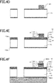
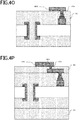
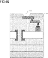
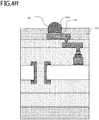
- Figs. 4A to 4R schematic illustrate the manufacturing process of a multilayer circuit board 3 including a glass core 2 having a through-hole according to an aspect of the present invention.
- a sputtered laminated film of a titanium layer 20A and a copper layer 20B are formed in order from the glass side as the first metal layers 20.
- the first metal layers 20 may cover part of the inside of the through-hole TH.
- a dry film resist is laminated on the copper layer 20B on the glass main surface 10a using a roll laminator or the like, and a first resist layer RE1 having an opening RE1A is formed by photolithography. Moreover, the same method is used to form a second resist layer RE2 on the glass main surface 10b.
- the first resist layer RE1 or the second resist layer RE2 may fill the through-hole TH in this step.
- the electrolytic copper plating layer 30 is formed in the opening RE1A illustrated in Fig. 4B .
- the plating may also be performed in, for example, a copper pyrophosphate plating bath.
- the first resist layer RE1 and the second resist layer RE2 are stripped way a sodium hydroxide solution, a TMAH solution, or the like.
- an adhesive layer 40ad, the dielectric layer 40, and a titanium layer 50A and a copper layer 50B as the second metal layer 50 are stacked in this order on the main surface 10a of the glass plate 10, by sputtering or CVD.
- the adhesive layer 40ad be a titanium layer. However, the adhesive layer may not be provided.
- a dry film resist is laminated using a roll laminator or the like, and a third resist layer RE3 is provided on the copper layer 50B and a fourth resist layer RE4 is provided on the copper layer 20B by photolithography.
- the third resist layer RE3 acts as a protective layer for preventing etching of areas other than target areas.
- a region of the copper layer 50B not covered with the third resist layer RE3 on the glass main surface 10a side is removed with a first etching agent, the titanium layer 50A is removed with a second etching agent, the dielectric layer 40 is removed by dry etching, and the adhesive layer 40ad is removed, to obtain the substrate illustrated in Fig. 4G .
- the adhesive layer 40ad is made of titanium, it is etched with the second etching agent
- the first etching agent is preferably an acid aqueous solution with a pH within the range of 0.5 or more and 2 or less.
- the acid aqueous solution preferably contains at least one of sulfuric acid and aqueous hydrogen peroxide, and more preferably contains both of them.
- the temperature of the first etching agent is preferably within the range of 20°C or more and 40°C or less, and more preferably in the range of 25°C or more and 35°C or less.
- the second etching agent is preferably a weak alkaline aqueous solution with a pH within the range of 7 or more and 12 or less, and more preferably a weak alkaline aqueous solution with a pH within the range of 8 or more and 10 or less.
- the weak alkaline solution is preferably a mixture of ammonia water and aqueous hydrogen peroxide.
- the temperature of the second etching agent is preferably within the range of 20°C or more and 40°C or less, and preferably in the range of 25°C or more and 35°C or less.
- the first and second etching agents range from acidic to weak alkaline, and can be used near room temperature, the glass is not damaged.
- the third resist layer RE3 and the fourth resist layer RE4 is stripped away using a sodium hydroxide solution, a TMAH solution, or the like, as illustrated in Fig. 4H , and the electroless nickel plating layer 60 is formed on the entire substrate including in the through-hole TH.
- the electroless nickel plating layer 60 serves as the seed layer of the second electrolytic copper plating layer 70 illustrated in Fig. 4J .
- An electroless nickel plating solution includes metallic salt containing nickel and a reducing agent.
- the metallic salt containing nickel can be nickel sulfate, nickel chloride, or a mixture of them, for example.
- the density of the metallic salt containing nickel included in the electroless nickel plating solution is preferably within the range of 10 or more and 50 g/L or less, more preferably within the range of 15 or more and 45 g/L or less, and further preferably within the range of 20 or more and 30 g/L or less.
- the reducing agent reduces the metallic salt containing nickel.
- the reducing agent can be formalin, hydrazine, hypophosphorous acid, sodium hypophosphite, sodium borohydride, or a mixture of them, for example. However, it is preferable to use hypophosphorous acid, sodium hypophosphite, or a mixture of these.
- the density of the reducing agent included in the electroless nickel plating solution is preferably within the range of 10 or more and 50 g/L or less, more preferably within the range of 15 or more and 45 g/L or less, and further preferably within the range of 20 or more and 30 g/L or less.
- the electroless nickel plating solution may further include a metal-based additive, an organic additive, a complexing agent, a pH adjusting agent, a buffering agent, or a mixture thereof.
- the metal-based additive enhances the stability of the electroless nickel plating solution.
- the metal-based additive contains lead, bismuth, or a mixture of these.
- the organic additive facilitates the precipitation of nickel.
- the organic additive contains sulfur, for example.
- the complexing agent can be ammonium hydroxide, sodium citrate, ethylene glycol, or a mixture of them, for example.
- the density of the complexing agent included in the electroless nickel plating solution is preferably within the range of 10 or more and 50 g/L or less, more preferably within the range of 10 or more and 40 g/L or less, and further preferably within the range of 20 or more and 30 g/L or less.
- the pH adjusting agent can be sodium hydroxide, ammonia, sulfuric acid, or a mixture of them, for example.
- the buffering agent can be sodium citrate, boric acid, carbonic acid, or a mixture of them.
- the electroless nickel plating solution may contain ammonium chloride.
- the density of the ammonium chloride included in the electroless nickel plating solution is preferably within the range of 10 or more and 50 g/L or less, more preferably within the range of 10 or more and 40 g/L or less, and further preferably within the range of 20 or more and 30 g/L or less.
- the pH of the electroless nickel plating solution is preferably within the range of 6 or more and 10 or less, more preferably in the range of 8.0 or more and 9.5 or less.
- the temperature of the electroless nickel plating solution is preferably within the range of 30°C or more and 60°C or less.
- the formulation of the above-described electroless nickel plating solution obtains an electroless nickel plating film having a phosphorus content within the range of 0.5 or more and less than 5 mass%.
- a dry film resist is laminated on using a roll laminator or the like, and a fifth resist layer RE5 having openings RE5A and RE5B and a sixth resist layer RE6 having an opening RE6A are formed on the electroless nickel plating layer 60 by photolithography.
- the second electrolytic copper plating layer 70 is formed in the openings RE5A, RE5B, and RE6A.
- the fifth resist layer RE5 and the sixth resist layer RE6 are stripped way the substrate illustrated in Fig. 4J in a sodium hydroxide solution, a TMAH solution, or the like, and the electroless nickel plating layer 60 and the copper layer 20B are etched with the first etching agent and the titanium layer 20A is etched with the second etching agent, to obtain the substrate illustrated in Fig. 4K .
- insulating layers 80 are bonded to both the glass main surface 10a and the glass main surface 10b with a vacuum-press laminator to form a resin plug PL in the through-hole TH, and the a via 80V is formed with laser or the like.
- the seed layer 80s is formed by an electroless nickel plating film or an electroless copper plating film.
- a method the same as that described above is used to form a seventh resist layer RE7 having an opening RE7A and an eighth resist layer RE8, and to form an electrolytic copper plating layer 80C in the opening RE7A.
- the seventh resist layer RE7 and the eighth resist layer RE8 are stripped away in a sodium hydroxide solution, a TMAH solution, or the like, and unnecessary parts of the seed layer 80s is etched, as illustrated in Fig. 4O .
- a substrate including a resin layer 90, a via 90V, a seed layer 90s, and an electrolytic copper plating layer 90C, as illustrated in Fig. 4P .
- solder resist layer 100 having an opening 100A is formed, as illustrated in Fig. 4Q .
- the solder resist is applied with a roll coater in the case of a liquid resist, or is formed with a laminator in the case of dry film, and then an opening is formed by photolithography.
- a surface-treatment layer 110 is provided in the opening 100A provided in the solder resist layer, and a solder layer 120 is provided, as illustrated in Fig. 4R .
- the first solder layer 120 can be formed by a publicly known method such as screen printing, solder ball transfer mounting, or electrolytic plating.
- the multi-layer circuit board 3 illustrated in Fig. 3 including the glass core 2 ( Fig. 2 ) can be obtained.
- the second electrolytic copper plating layer 70 can be reliably formed above the dielectric layer 40, and in this way, the multi-layer circuit board can be formed.
- the step of forming the electrolytic copper plating layer 70 in the through-hole TH immediately before the resin plug PL in the through-hole TH the accumulation of stress from the copper applied to the through-hole TH over time can be mitigated, in comparison with a case in which the electrolytic copper plating layer is formed in a through-hole TH simultaneously with the first electrolytic copper plating layer 30, and the risk of glass breakage can be reduced.
- the roughness of the surface of the glass plate 10 obtained by using a contactless interference microscope is 0.5 nm before the start of manufacture, and 0.55 nm after the manufacture. Therefore, such a manufacturing method can suppress damage to the glass, that is, the risk of glass breakage in the manufacturing process can be reduced.
- the dry etching of the dielectric layer 40 is preferably performed in a state in which the pattern density is low as possible.
- the second electrolytic copper plating layer around the through-hole TH is formed after dry etching, the pattern density on the glass surface during dry etching is low.
- the surface configuration of the substrate facilitates dry etching, and thereby failure in dry etching can be reduced.
- failure in the formation of an electrolytic copper plating layer on the dielectric layer provided above the glass core can be prevented. Furthermore, by using an acidic etching agent on an electroless nickel plating film having a phosphorus content of less than 5 mass%, glass breakage can be effectively prevented, and by mitigating the accumulation of stress to the through-hole in the glass, cracking in the through-hole in the manufacturing process can be suppressed.
- the present invention is not limited to the embodiments and modification examples described above. Besides, various modification examples can be carried out without deviating from the gist of the present invention.
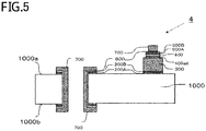
- a glass core 4 illustrated in Fig. 5 was manufactured in accordance with the manufacturing process illustrated in Figs. 6A to 6I .
- a 200- ⁇ m thick, 500 ⁇ 500-mm glass panel 1000 (EAGLE XG available from Corning Incorporated) with a through-hole TH was prepared.
- the roughness of the surface of the glass plate 1000 measured by a contactless interference microscope was 0.5 nm.
- the diameter of the through hole TH formed in the glass plate 1000 was 80 ⁇ m on the first main surface of the glass plate 1000 and was 60 ⁇ m on the second main surface of the glass plate 1000. Note that the diameters are the same in the drawings.
- a 50-nm titanium layer 200A and a 300-nm copper layer 200B were formed in this order on one of the main surfaces of the glass plate 1000 as a first metal layer 200 by sputtering.
- a first resist layer RE10 and a second resist layer RE20 were formed.
- a 500 ⁇ 500- ⁇ m opening RE10A is formed, and a first electrolytic copper plating layer 300 was deposited in the opening RE10A with a thickness of 10 ⁇ m by electrolytic plating.
- the substrate obtained in the step in Fig. 6B was immersed in a 5% sodium hydroxide aqueous solution at 50°C to strip the first resist layer RE10 and the second resist layer RE20, and the substrate in Fig. 6C was obtained.
- a 50-nm thick titanium layer was formed as an adhesive layer 400ad
- a 200-nm thick aluminum oxide layer was formed as a dielectric layer 400
- a 50-nm thick titanium layer 500A was formed as a second metal layer 500
- a 300-nm thick copper layer 500B was formed, in this order.
- a 400 ⁇ 400- ⁇ m resist layer RE30 which is slightly smaller than the electrode size 500 ⁇ 500 ⁇ m of the first electrolytic copper plating layer 30, was formed by lamination and photolithography using a photosensitive dry film resist.
- a dry film resist layer RE40 was formed on one of the glass main surface 1000a and the main surface 1000b opposing the glass main surface 1000a.
- a 300-nm thick copper layer 500B, a 50-nm thick titanium layer 500A, an aluminum oxide layer serving as the 200-nm thick dielectric layer 400, and a 50-nm thick titanium layer 400ad formed on an area of the glass main surface not protected with the resist layer RE30 were etched in this order.
- the copper layer 500B was etched using a mixed solution of sulfuric acid and hydrogen peroxide (pH 1, temperature 25°C), which served as a first etching agent.
- the titanium layer 500A and the titanium layer 400ad were etched using a mixed solution of hydrogen peroxide and aqueous ammonia (pH 9, temperature 25°C), which served as a second etching agent.
- the aluminum oxide layer serving as the 200-nm thick dielectric layer 400 was removed by dry etching.
- the substrate illustrated in Fig. 6F was immersed in a 5% sodium hydroxide aqueous solution at 50°C to strip the resist layer RE30 and the dry resist layer RE40. After stripping, the glass core was catalyzed by a solution including palladium. The glass core was then immersed in the following electroless nickel plating solution A to form an electroless nickel plating layer 600. In this way, the substrate illustrated in Fig. 6G was obtained.
- the bath configuration of the electroless nickel plating solution A is as follows. Bath Composition: Nickel sulfate 20 g/L, Sodium hypophosphite 25 g/L, Lactic acid 30 g/L, Lead ion 1 ppm (residue is deionized water) pH: 8.5 Temperature: 40°C
- the thickness of the electroless nickel plating layer was measured to be 0.1 ⁇ m.
- the phosphorus contents of the electroless nickel plating layer measured by the method described above was 4 mass%.
- photosensitive dry film resist layers RE50 and RE60 having openings RE50A, RE50B, and RE60A were formed on the glass main surface and an opposing main surface by the same method described above, and a second electrolytic copper plating layer 700 was formed by electrolytic plating. At this time, the thickness of the second electrolytic copper plating layer 700 was approximately 10 ⁇ m.
- the resist layer RE50 and the resist layer RE60 were stripped away in a 5% sodium hydroxide aqueous solution at 50°C.
- the electroless nickel plating layer 600 and the copper layer 200B were etched using a mixed solution of sulfuric acid and hydrogen peroxide (pH 1, temperature 25°C), which served as a first etching agent.
- the titanium layer 200A was etched using a mixed solution of hydrogen peroxide and aqueous ammonia (pH 9, temperature 25°C), which served as a second etching agent.
- the glass core 4 illustrated in Fig. 5 was obtained.
- Example 2 a glass core was manufactured by the same method as that for the bath configuration of the electroless nickel plating A according to Example 1 except that the pH was 9, and the temperature was 50°C. The plating time was adjusted so that the thickness of the electroless nickel plating layer reached 0.1 ⁇ m.
- the thickness of the electroless nickel plating layer manufactured in this example was measured to be 0.1 ⁇ m.
- the phosphorus content of the electroless nickel plating layer measured by the method described above was 1 mass%.
- Comparative Example 1 a glass core was manufactured by the same method as that in Example 1 except that the following electroless nickel plating solution B was used as an electroless nickel plating solution to form an electroless nickel plating layer having a phosphorus content of 6 mass%.
- the following third etching agent was used as the etching agent of the electroless nickel plating layer.
- the bath configuration of the electroless nickel plating solution B is as follows.
- the third etching agent is composed of a solution including 25% sodium hydroxide (pH 14, 80°C).
- a glass plate that is the same as in Example 1 was used: a titanium layer 200A, a copper layer 200B, and an electroless nickel plating layer 600 were stacked on the glass 1000 in this order; the electroless nickel plating layer 600 was formed in a through-hole TH; a resist was provided by the same method as that in Example 1; an electrolytic copper plating layer 300 was formed on the electroless nickel plating layer 600; and the resist layer was stripped away to obtain the substrate illustrated in Fig. 7A .
- the electroless nickel plating solution A was used as an electroless nickel plating solution.
- a 50-nm thick titanium layer was formed as an adhesive layer 400ad, a 200-nm thick aluminum oxide layer was formed as a dielectric layer 400, a 50-nm thick titanium layer 500A was formed as a second metal layer 500, and a 300-nm thick copper layer 500B was formed, in this order on the glass main surface 100a; and a predetermined region was protected with a resist. Furthermore, a 300-nm thick copper layer 500B that was not protected by the resist layer and unwanted, a 50-nm thick titanium layer 500A, a dielectric layer serving as a 200-nm thick aluminum oxide layer 400, and a 50-nm thick titanium layer 400ad were sequentially etched.
- the copper layer 500B was etched using a mixed solution of sulfuric acid and hydrogen peroxide (pH 1, temperature 25°C), which serves as a first etching agent; the titanium layer 500A and the titanium layer 400ad were etched using a mixed solution of hydrogen peroxide and aqueous ammonia (pH 9, temperature 25°C), which serves as a second etching agent; and the dielectric layer serving as the 200-nm thick aluminum oxide layer 400 was removed by dry etching. In this way, the substrate illustrated in Fig. 7B was obtained.
- An electrolytic copper plating layer 700 was provided on the copper layer 500B by the same method as that in Example 1, to obtain the substrate illustrated in Fig. 7C .
- Each of the glass cores manufactured in the examples and the comparative examples were evaluated for the formation of an electrolytic copper plating layer on a dielectric layer, cracking in the through-hole formed in the glass, and breakage of the glass panel.
- Table 1 shows the evaluation results of Examples 1 and 2 and Comparative Examples 1 and 2. In the evaluation results, a pass rate of 100% is defined as "good,” and a pass rate of less than 100% is defined as “poor.” The pass rate is shown together with the ratio of the number of defects to the number of samples (number of defects/number of samples).
- Items Example 1 Example 2 Comparative Example 1 Comparative Example 2 Cross-sectional Structure of Examples and Comparative Examples In the structure illustrated in Fig. 6I the electroless nickel plating layer 60 is provided directly under the first electrolytic copper plating layer 300 and the second electrolytic copper plating layer 700. In the structure illustrated in Fig. 7C the electroless nickel plating layer 600 is only provided directly under the first electrolytic copper plating layer 300.
- Type of electroless nickel plating solution A A B A Phosphorus Content 4 1 6 4 Etching Agent for Electroless Nickel Plating Layer First Etching Agent (Acid) First Etching Agent (Acid) Third Etching Agent (Alkaline) First Etching Agent (Acid) Formation of Electrolytic Copper Plating Layer on Dielectric Layer Good 100/100 OK Good 100/100 OK Poor 90/100 OK Poor 92/100 OK Cracking in Through-hole Good 100/100 OK Good 100/100 OK Poor 95/100 OK Poor 95/100 OK Breakage of Glass Panel Good 10/10 OK Good 10/10 OK Poor 9/10 OK Good 10/10 OK
- the electrolytic copper plating layer can be formed on the dielectric layer with a probability of 100%. No glass cracking inside the through-hole or breakage of the glass panel surface was observed.
Landscapes
- Engineering & Computer Science (AREA)
- Microelectronics & Electronic Packaging (AREA)
- Chemical & Material Sciences (AREA)
- Inorganic Chemistry (AREA)
- Manufacturing & Machinery (AREA)
- Ceramic Engineering (AREA)
- Production Of Multi-Layered Print Wiring Board (AREA)
- Parts Printed On Printed Circuit Boards (AREA)
- Laminated Bodies (AREA)
Abstract
Description
- The present invention relates to a glass core, a multilayer circuit board, and a method of manufacturing a glass core.
- In recent years, electronic devices have become more sophisticated and compact. Accordingly, there has been a demand for increasing the density of semiconductor modules mounted on the electronic devices. To respond to such a demand, increasing the wiring density of a circuit board on which a semiconductor chip is mounted has been studied.
- Typically, a glass epoxy resin is used as a core material included in the circuit board. In recent years, a circuit board including a glass plate as a core material has attracted attention. A glass plate can achieve a higher degree of smoothness than a core material made of a glass epoxy resin. For this reason, ultrafine wires can be formed on a circuit board including a glass plate, and, thus, high-density implementation is possible by using a circuit board including a glass plate. The coefficient of linear thermal expansion (CTE) of a glass plate, within the temperature range of 20°C or more and 260°C or less, almost coincides with the coefficient of linear thermal expansion of a semiconductor chip made of a silicon substrate within the temperature range of 20°C or more and 260°C or less. Therefore, the use of a circuit board including a glass plate allows implementation with reduced residual stress. Furthermore, a circuit board including a glass plate is advantageous in that it is excellent for high-speed communication. From the foregoing points, a circuit board including a glass plate has been attracting attention as a wiring substrate of semiconductor modules to be mounted in high-performance electronic devices.
- NPL 1: Takagi, Kiyoshi, Yokuwakaru purinto haisenban no dekirumade (Easy to Understand Manufacturing Processes for Printed Circuit Boards), 2nd Edition, April 2008, pp.201-202, Nikkan Kogyo Shimbun, Ltd.
- A circuit board or a portion of a circuit board is formed by forming wires on a glass plate. This is referred to as a glass core. When wires are formed on a glass plate, typically, a semi-additive process is applied (NPL 1). Such a process can be applied to provide an insulating resin layer after a conduction layer has been formed on a glass plate, and stack a conductor on the insulating resin layer, to form multiple layers of wires. However, when a dielectric layer is provided on a glass plate, it is difficult to apply a conventional semi-additive process. The reason for this will be described.
- There is a process of providing a seed layer on a glass plate, providing an electrolytic copper plating layer on the seed layer, etching unnecessary parts of the seed layer, providing a dielectric layer on the electrolytic copper plating layer, and further providing another electrolytic copper plating layer on the dielectric layer. According to the process, a dielectric layer can be provided without an insulating resin layer. However, an undercut in the electrolytic copper plating layer formed on the glass plate via the seed layer formed when unnecessary parts of the seed layer is etched causes a new issue in that the electrolytic copper plating layer cannot be formed on the dielectric layer.
- As a countermeasure, another process may be considered in which a metal layer formed by sputtering and a seed layer including an electroless nickel plating layer are formed on a glass plate, an electrolytic copper plating layer is formed on the electroless nickel plating layer, a dielectric layer is formed on the electrolytic copper plating layer on the glass plate, and another electrolytic copper plating layer is formed on the dielectric layer. Such a process can suppress the formation of an undercut in the electrolytic copper plating layer.
- However, when the phosphorus content in the electroless nickel plating layer is high, an alkaline etching agent should be used for etching of unnecessary parts of the electroless nickel plating layer. In such a case, there is problem in that the damage to the glass plate caused by the alkaline etching agent may cause the glass plate to break during the manufacturing process. Also, when an alkaline etching agent is used, there are cases in which a defect in the formation of the electrolytic copper plating layer on the dielectric layer occurs due to an undercut in the electrolytic copper plating layer formed on the glass plate via the glass plate.
- Furthermore, when a through-hole is formed in the glass plate for multilayer wiring and a seed layer including an electroless nickel plating layer is formed in the through-hole, there is a problem in that stress of the copper accumulates in the through-hole during etching of unnecessary parts of the seed layer if the thickness of the glass is small, and thereby glass cracking occur. To avoid such a problem, cracking need to be prevented by easing the stress of the copper applied to the glass plate by immediately forming an insulating resin layer after the electrolytic copper plating layer has been formed in the through-hole. Therefore, it is necessary to provide a step of providing an insulating resin layer immediately after the electrolytic copper plating layer has been formed in the through-hole, and this leads to a complicated manufacturing process.
- The present invention, which has been conceived in view of the above-described issue, provides a glass core, a multilayer circuit board, and a method of manufacturing a glass core that enables appropriate formation of copper wiring and suppresses cracking and the like.
- According to an aspect of the present invention, a glass core includes a glass plate; a first metal layer disposed on the glass plate; a first electrolytic copper plating layer disposed on the first metal layer; a dielectric layer disposed above the first electrolytic copper plating layer; a second metal layer disposed on the dielectric layer; an electroless nickel plating layer disposed on the second metal layer and having a phosphorus content of less than 5 mass%; and a second electrolytic copper plating layer disposed on the electroless nickel plating layer.
- According to an aspect of the present invention, a method of manufacturing a glass core, includes forming a first metal layer on a glass plate; forming a first electrolytic copper plating layer above the first metal layer; forming a dielectric layer on the first electrolytic copper plating layer; forming a second metal layer on the dielectric layer; forming an electroless nickel plating layer disposed on the second metal layer and having a phosphorus content of less than 5 mass%; forming a second electrolytic copper plating layer disposed on the electroless nickel plating layer; and removing unnecessary parts of the electroless nickel plating layer using an acidic etching agent.
- The embodiments of the present invention provide a glass core, a multilayer circuit board, and a method of manufacturing a glass core that enables appropriate formation of copper wiring and suppresses cracking and the like.
-
-
Fig. 1 is a schematic cross-sectional view of aglass core 1 according to an aspect of the present invention. -
Fig. 2 is a schematic cross-sectional view of aglass core 2 having a through-hole according to an aspect of the present invention. -
Fig. 3 is a schematic cross-sectional view of amultilayer circuit board 3 including aglass core 2 having a through-hole according to an aspect of the present invention. -
Fig. 4A is a schematic cross-sectional view of the manufacturing process of amultilayer circuit board 3 including aglass core 2 having a through-hole according to an aspect of the present invention. -
Fig. 4B is a schematic cross-sectional view of the manufacturing process of amultilayer circuit board 3 including aglass core 2 having a through-hole according to an aspect of the present invention. -
Fig. 4C is a schematic cross-sectional view of the manufacturing process of amultilayer circuit board 3 including aglass core 2 having a through-hole according to an aspect of the present invention. -
Fig. 4D is a schematic cross-sectional view of the manufacturing process of amultilayer circuit board 3 including aglass core 2 having a through-hole according to an aspect of the present invention. -
Fig. 4E is a schematic cross-sectional view of the manufacturing process of amultilayer circuit board 3 including aglass core 2 having a through-hole according to an aspect of the present invention. -
Fig. 4F is a schematic cross-sectional view of the manufacturing process of amultilayer circuit board 3 including aglass core 2 having a through-hole according to an aspect of the present invention. -
Fig. 4G is a schematic cross-sectional view of the manufacturing process of amultilayer circuit board 3 including aglass core 2 having a through-hole according to an aspect of the present invention. -
Fig. 4H is a schematic cross-sectional view of the manufacturing process of amultilayer circuit board 3 including aglass core 2 having a through-hole according to an aspect of the present invention. -
Fig. 4I is a schematic cross-sectional view of the manufacturing process of amultilayer circuit board 3 including aglass core 2 having a through-hole according to an aspect of the present invention. -
Fig. 4J is a schematic cross-sectional view of the manufacturing process of amultilayer circuit board 3 including aglass core 2 having a through-hole according to an aspect of the present invention. -
Fig. 4K is a schematic cross-sectional view of the manufacturing process of amultilayer circuit board 3 including aglass core 2 having a through-hole according to an aspect of the present invention. -
Fig. 4L is a schematic cross-sectional view of the manufacturing process of amultilayer circuit board 3 including aglass core 2 having a through-hole according to an aspect of the present invention. -
Fig. 4M is a schematic cross-sectional view of the manufacturing process of amultilayer circuit board 3 including aglass core 2 having a through-hole according to an aspect of the present invention. -
Fig. 4N is a schematic cross-sectional view of the manufacturing process of amultilayer circuit board 3 including aglass core 2 having a through-hole according to an aspect of the present invention. -
Fig. 4O is a schematic cross-sectional view of the manufacturing process of amultilayer circuit board 3 including aglass core 2 having a through-hole according to an aspect of the present invention. -
Fig. 4P is a schematic cross-sectional view of the manufacturing process of amultilayer circuit board 3 including aglass core 2 having a through-hole according to an aspect of the present invention. -
Fig. 4Q is a schematic cross-sectional view of the manufacturing process of amultilayer circuit board 3 including aglass core 2 having a through-hole according to an aspect of the present invention. -
Fig. 4R is a schematic cross-sectional view of the manufacturing process of amultilayer circuit board 3 including aglass core 2 having a through-hole according to an aspect of the present invention. -
Fig. 5 is a schematic cross-sectional view of aglass core 4 according to an example of the present invention. -
Fig. 6A is a schematic cross-sectional view of a manufacturing process of aglass core 4 according to an example of the present invention. -
Fig. 6B is a schematic cross-sectional view of a manufacturing process of aglass core 4 according to an example of the present invention. -
Fig. 6C is a schematic cross-sectional view of a manufacturing process of aglass core 4 according to an example of the present invention. -
Fig. 6D is a schematic cross-sectional view of a manufacturing process of aglass core 4 according to an example of the present invention. -
Fig. 6E is a schematic cross-sectional view of a manufacturing process of aglass core 4 according to an example of the present invention. -
Fig. 6F is a schematic cross-sectional view of a manufacturing process of aglass core 4 according to an example of the present invention. -
Fig. 6G is a schematic cross-sectional view of a manufacturing process of aglass core 4 according to an example of the present invention. -
Fig. 6H is a schematic cross-sectional view of a manufacturing process of aglass core 4 according to an example of the present invention. -
Fig. 6I is a schematic cross-sectional view of a manufacturing process of aglass core 4 according to an example of the present invention. -
Fig. 7A is a schematic cross-sectional view of a manufacturing process of a glass core according to a comparative example of the present invention. -
Fig. 7B is a schematic cross-sectional view of a manufacturing process of a glass core according to a comparative example of the present invention. -
Fig. 7C is a schematic cross-sectional view of a manufacturing process of a glass core according to a comparative example of the present invention. - Hereinafter, aspects of the present invention will be described with reference to the drawings. In the following description, components with identical elements or identical functions will be given identical reference signs, and redundant description thereof will be omitted.
- Note that, in the specification, the term "above (upper)" refers to being farther from the glass plate, and the term "below (under)" refers to being closer to the glass plate.
-
Fig. 1 is a schematic cross-sectional view of aglass core 1 according to an aspect of the present invention. - The
glass core 1 illustrated inFig. 1 includes aglass plate 10, afirst metal layer 20, a first electrolyticcopper plating layer 30, adielectric layer 40, asecond metal layer 50, an electrolessnickel plating layer 60, and a second electrolyticcopper plating layer 70. - The
glass plate 10 typically has light permeability. There are no particular limitations on the components and their ratios of a glass material for theglass plate 10. Theglass plate 10 can be made from glass having silicate as the main component, such as alkali-free glass, alkali glass, borosilicate glass, quartz glass, sapphire glass, or light-sensitive glass, for example. From the viewpoint of being used for a semiconductor package and a semiconductor module, theglass plate 10 is desirably made from alkali-free glass. The alkali component content of the alkali-free glass is preferably 0.1 mass% or less. - The thickness of the
glass plate 10 is preferably 1 mm or less. The thickness of theglass plate 10 is more preferably within the range of 0.1 or more and 0.8 mm or less, in consideration of ease of handling during manufacture. - Examples of a method for manufacturing the
glass plate 10 include a float method, a down-draw method, a fusion method, an up-draw method, and a roll-out method. Theglass plate 10 may be produced by any of the foregoing methods. - The coefficient of linear thermal expansion (CTE) of the
glass plate 10 is preferably within the range of 0.5 × 10⁻⁶/K or more and 15.0 × 10⁻⁶/K or less in the temperature range of 20°C or more and 260°C or less, preferably within the range of 1.0 × 10⁻⁶/K or more and 8.0 × 10⁻⁶/K or less, and further preferably within the range of 1.0 × 10⁻⁶/K or more and 4.0×10⁻⁶/K or less. When the coefficient of linear thermal expansion of theglass plate 10 is in this range, the difference from the coefficient of linear thermal expansion of a semiconductor chip including a silicon substrate to be mounted on the surface of thecore substrate 1 tends to be small. The coefficient of linear thermal expansion refers to the ratio of change in length corresponding to temperature rise. - At least the first main surface of the
glass plate 10 may include a functional layer. Examples of the functional layer include an antireflection layer containing fine particles, an infrared shielding layer containing an infrared absorbing agent, a strength imparting layer containing a hard coat material, an antistatic layer containing an antistatic agent, a color layer containing a coloring agent, an optical filter layer containing an optical thin film, a texture control layer and an antiglare layer containing a light scattering film. These functional layers can be formed by surface treatment techniques such as evaporation, sputtering, or wet-spraying, for example. - The
first metal layer 20 and thesecond metal layer 50 are typically formed by sputtering or chemical vapor deposition (CVD). - The
first metal layers 20 and thesecond metal layer 50 may be formed from, for example, copper (Cu), aluminum (Al), titanium (Ti), chromium (Cr), molybdenum (Mo), tungsten (W), tantalum (Ta), gold (Au), iridium (Ir), ruthenium (Ru), palladium (Pd), platinum (Pt), Al-Si alloy, Al-Si-Cu alloy, Al-Cu alloy, Ni-Fe alloy, indium tin oxide (ITO), indium zinc oxide (IZO), active zinc oxide (AZO), zinc oxide (ZnO), lead zirconate titanate (PZT), titanium nitride (TiN), Cu3N4, Cu alloy, a mixture of these, a monolayer film, or a laminated film. - The
first metal layer 20 is preferably a sputtered laminated film of titanium and copper, i.e., a laminate of a titanium layer and a copper layer formed separately by sputtering. The titanium layer can enhance the adhesion with theglass plate 10. The copper layer can enhance the adhesion of the titanium layer and the electrolyticcopper plating layer 30. That is, by forming themetal layer 20 as a sputtered laminated film of titanium and copper, the first electrolyticcopper plating layer 30 having satisfactory adhesiveness can be formed on theglass plate 10. - The
second metal layer 50 is also preferably a sputtered laminated film of titanium and copper, like thefirst metal layer 20. The titanium layer can enhance the adhesion with thedielectric layer 40. By providing a copper layer having satisfactory adhesion with the titanium layer on the titanium layer, an electrolessnickel plating layer 60 can be provided on the copper layer. - When the
first metal layer 20 and thesecond metal layer 50 are sputtered laminated films of titanium and copper, the thickness of the titanium layer is preferably within the range of 0.01 or more and 0.1 µm or less. The thickness of the copper layer is preferably within the range of 0.09 or more and 0.5 µm of less. If any of these values is lower than a lower limit value, the throwing power relative to the base material is lowered and the film is undesirably accompanied by pinholes. If the values exceed an upper limit value, no enhancement of performance is observed, and this is not preferable in terms of cost. - A sputtered layer, such as titanium, for example, may be provided as an adhesive layer between the first electrolytic
copper plating layer 30 and thedielectric layer 40. - The film of the electroless
nickel plating layer 60 contains phosphorus (P). The phosphorus content in the plating film is preferably within the range of 0.1 mass% or more and less than 5 mass %, more preferably within the range of 0.5 mass% or more and less than 5 mass%, but 0 mass% or more can be sufficient. - When the phosphorus content in the film of the electroless
nickel plating layer 60 is within the range of 0.1 mass% or more and less than 5 mass%, an acid etching agent can be used to etch the electroless nickel plating layer that is not needed in the manufacturing process. In this way, glass corrosion and damage to the dielectric layer during etching can be prevented. In contrast, when the phosphorus content is 5 mass% or more, an alkaline etching agent must be used under a high temperature condition to etch the electroless nickel plating layer that is not needed in the manufacturing process. Therefore, glass corrosion or damage to the dielectric layer may occur during etching. Therefore, to prevent glass from cracking and to obtain capacitor characteristics, the phosphorus content of the film of the electrolessnickel plating layer 60 is preferably within the range of 0.1 (preferably 0.5) mass% or more up to 5 mass%. - The phosphorus content of the film of the electroless
nickel plating layer 60 can be obtained by X-ray fluorescence elemental analysis (XRF), such as energy-dispersive X-ray analysis (EDX), for example. - The film of the electroless
nickel plating layer 60 may contain other components such as sulfur (S), lead (Pb), and bismuth (Bi) in addition to nickel and phosphorus. - The thickness of the electroless
nickel plating layer 60 is typically 1 µm or less, desirably 0.4 µm or less, more desirably 0.3 µm or less, further desirably 0.1 µm or less. If the thickness of the electrolytic nickel plating layer 24 is small, the time required for the formation and etching of the electrolessnickel plating layer 60 is reduced, thereby facilitating the manufacturing. - The thickness of the electroless
nickel plating layer 60 can be obtained by X-ray fluorescence elemental analysis, for example. - The interface of the
second metal layer 50 and the electrolessnickel plating layer 60 includes palladium, or palladium and tin. The palladium and tin act as a catalyst during formation of an electroless nickel plating film. Furthermore, thesecond metal layer 50 and the interface including palladium may further include an adhesive layer for enhancing the adhesion between the electrolessnickel plating layer 60 and thesecond metal layer 50. - An electroless copper plating layer cannot replace the electroless
nickel plating layer 60. This is because an electroless copper plating bath has a high pH of approximately 12. Thus, an electroless copper plating layer provided on a dielectric layer damages the dielectric layer. Furthermore, the electroless copper plating layer has poor adhesion to the glass, and the electroless copper plating film deposited at the end of the glass is stripped away in the electroless copper plating bath thereby undesirably promoting decomposition of the electroless copper plating bath. - The thicknesses of the first electrolytic
copper plating layer 30 and the second electrolyticcopper plating layer 70 desirably are within the range of 1 or more and 20 µm or less, and more preferably within the range of 3 or more and 18 µm or less. - The
dielectric layer 40 may contain an inorganic compound, for example. Examples of the inorganic compound include oxides, carbides, nitrides, and borides containing at least one kind of element selected from the group consisting of aluminum, titanium, tantalum, chromium, lanthanum, samarium, ytterbium, yttrium, gadolinium, zirconium, niobium, hafnium, gallium, cerium, and silicon. - The
dielectric layer 40 desirably contains at least one of silicon nitride, tantalum oxide, and aluminum oxide. Silicon nitride, tantalum oxide, and aluminum oxide are low in dielectric constant and are excellent in insulation properties. - The
dielectric layer 40 is typically formed by sputtering or chemical vapor deposition (CVD). - The
first metal layer 20, the first electrolyticcopper plating layer 30, thedielectric layer 40, thesecond metal layer 50, the electrolessnickel plating layer 60, and the second electrolyticcopper plating layer 70, as illustrated inFig. 1 , are provided on a glassmain surface 10a. However, these may be provided on a glassmain surface 10b opposing the glassmain surface 10a, or on both the glassmain surfaces - A conduction layer below the
dielectric layer 40 including thefirst metal layer 20 and the first electrolyticcopper plating layer 30, thedielectric layer 40, and a conduction layer above thedielectric layer 40 including thesecond metal layer 50, the electrolessnickel plating layer 60, and the second electrolytic copper plating layer form a capacitor. -
Fig. 2 is a schematic cross-sectional view of aglass core 2 having a through-hole according to an aspect of the present invention. - The
glass core 1 illustrated inFig. 2 includes aglass plate 10, a through-hole TH, afirst metal layer 20, a first electrolyticcopper plating layer 30, adielectric layer 40, asecond metal layer 50, an electrolessnickel plating layer 60, and a second electrolyticcopper plating layer 70. - The shape of a cross section of the through hole TH in the axial direction may be a rectangle, an X shape in which the diameter of the center part of the through hole TH is smaller than that at a first end and a second end, a tapered shape in which the bottom diameter of the through hole TH is smaller than the diameter at the first end , an O shape in which the diameter of the center part of the through hole TH is larger than the diameter at the first end and the diameter at the second, or any other shape. Moreover, the shape of a cross section of the through hole TH orthogonal to the axial direction may be a circle, an oval, or a polygon.
- By providing a conduction layer including the electroless
nickel plating layer 60 and the second electrolyticcopper plating layer 70 in the through-hole TH, the glassmain surface 10a and the glassmain surface 10b can be made electrically conductive with each other. A portion of the through-hole TH may be covered with the first metal layer. - The portion between the inner wall of the through-hole TH and the electroless
nickel plating layer 60 includes palladium, or palladium and tin. The palladium and tin act as a catalyst during electroless nickel plating. Furthermore, the inner wall of the through-hole TH and the interface including palladium may further include an adhesive layer for enhancing the adhesion between the electrolessnickel plating layer 60 and the glass in the through-hole TH. -
Fig. 3 is a schematic cross-sectional view of amultilayer circuit board 3 including aglass core 2 having a through-hole according to an aspect of the present invention. - The multilayer circuit board illustrated in
Fig. 3 includes theglass core 2 as a base, and further includes aglass plate 10, afirst metal layer 20, a first electrolyticcopper plating layer 30,adielectric layer 40, asecond metal layer 50, an electrolessnickel plating layer 60, and a second electrolyticcopper plating layer 70, afirst resin layer 80, asecond resin layer 90, a plug PL made of resin, a solder resistlayer 100, a via 80V, a via 90V, aseed layer 80s, aseed layer 90s, an electrolyticcopper plating layer 80C, an electrolyticcopper plating layer 90C, a surface-treatment layer 110, and asolder layer 120. - The
first resin layer 80 and thesecond resin layer 90 may be made of any of an epoxy resin, a polyimide resin, a maleimide resin, polyethylene terephthalate, polyphenylene oxide, liquid crystal polymer, or a composite material of them. The resin is desirably an epoxy resin containing a filler from the viewpoints of electrical characteristics and the ease of manufacture. The filler can be silica, barium sulfate, titanium oxide, or a mixture of them, for example. The resin may be a conductive paste or a conductive resin. - The plug PL is formed by filling, with resin, a hollow portion in the through-hole TH not filled with the electroless
nickel plating layer 60 and the second electrolyticcopper plating layer 70, and is integrated with thefirst resin layer 80. - The via 80V and the via 90V are formed by processing the
first resin layer 80 and thesecond resin layer 90 with a laser or the like if thefirst resin layer 80 and thesecond resin layer 90 are made of a non-photosensitive material, and by photolithography in the case where they are made of a photosensitive material. - The seed layers 80s and 90s are preferably electrolytic nickel plating films or electroless copper plating films. Alternatively, nickel or copper may be deposited into a film by sputtering.
- For the
surface treatment layer 110, a plating film such as tin plating, tin alloy plating, electroless Ni-P/electroless Pd-P/Au plating, or electroless Ni-P/Au plating may be used. Thesurface treatment layer 110 may use organic films instead of plating films. The organic films may be pre-solder treatment films or pre-flux treatment films such as organic solderability preservative (OSP). - The
solder layer 120 is provided on thesurface treatment layer 110. Thesolder layer 120 contains tin, silver, copper, bismuth, lead, zinc, indium, antimony, or a mixture of them. -
Figs. 4A to 4R schematic illustrate the manufacturing process of amultilayer circuit board 3 including aglass core 2 having a through-hole according to an aspect of the present invention. - First, on the glass
main surface 10a and themain surface 10b opposing the glassmain surface 10a of theglass plate 10 having a through-hole TH, as illustrated inFig. 4A , a sputtered laminated film of atitanium layer 20A and acopper layer 20B are formed in order from the glass side as the first metal layers 20. The first metal layers 20 may cover part of the inside of the through-hole TH. - Next, as illustrated in
Fig. 4B , a dry film resist is laminated on thecopper layer 20B on the glassmain surface 10a using a roll laminator or the like, and a first resist layer RE1 having an opening RE1A is formed by photolithography. Moreover, the same method is used to form a second resist layer RE2 on the glassmain surface 10b. - Since the first resist layer RE1 or the second resist layer RE2 is stripped away in subsequent processing, the first resist layer RE1 or the second resist layer RE2 may fill the through-hole TH in this step.
- Next, as illustrated in
Fig. 4C , the electrolyticcopper plating layer 30 is formed in the opening RE1A illustrated inFig. 4B . Although it is preferable that electrolytic copper plating be performed in a copper sulfate plating bath, which is inexpensive and easy to control, the plating may also be performed in, for example, a copper pyrophosphate plating bath. - Next, as illustrated in
Fig. 4D , the first resist layer RE1 and the second resist layer RE2 are stripped way a sodium hydroxide solution, a TMAH solution, or the like. - Next, as illustrated in
Fig. 4E , an adhesive layer 40ad, thedielectric layer 40, and atitanium layer 50A and acopper layer 50B as thesecond metal layer 50 are stacked in this order on themain surface 10a of theglass plate 10, by sputtering or CVD. - It is preferable that the adhesive layer 40ad be a titanium layer. However, the adhesive layer may not be provided.
- Next, as illustrated in
Fig. 4F , a dry film resist is laminated using a roll laminator or the like, and a third resist layer RE3 is provided on thecopper layer 50B and a fourth resist layer RE4 is provided on thecopper layer 20B by photolithography. The third resist layer RE3 acts as a protective layer for preventing etching of areas other than target areas. - Next, a region of the
copper layer 50B not covered with the third resist layer RE3 on the glassmain surface 10a side is removed with a first etching agent, thetitanium layer 50A is removed with a second etching agent, thedielectric layer 40 is removed by dry etching, and the adhesive layer 40ad is removed, to obtain the substrate illustrated inFig. 4G . In the case where the adhesive layer 40ad is made of titanium, it is etched with the second etching agent - The first etching agent is preferably an acid aqueous solution with a pH within the range of 0.5 or more and 2 or less. The acid aqueous solution preferably contains at least one of sulfuric acid and aqueous hydrogen peroxide, and more preferably contains both of them.
- The temperature of the first etching agent is preferably within the range of 20°C or more and 40°C or less, and more preferably in the range of 25°C or more and 35°C or less.
- The second etching agent is preferably a weak alkaline aqueous solution with a pH within the range of 7 or more and 12 or less, and more preferably a weak alkaline aqueous solution with a pH within the range of 8 or more and 10 or less. The weak alkaline solution is preferably a mixture of ammonia water and aqueous hydrogen peroxide.
- The temperature of the second etching agent is preferably within the range of 20°C or more and 40°C or less, and preferably in the range of 25°C or more and 35°C or less.
- Since the first and second etching agents range from acidic to weak alkaline, and can be used near room temperature, the glass is not damaged.
- Next, the third resist layer RE3 and the fourth resist layer RE4 is stripped away using a sodium hydroxide solution, a TMAH solution, or the like, as illustrated in
Fig. 4H , and the electrolessnickel plating layer 60 is formed on the entire substrate including in the through-hole TH. The electrolessnickel plating layer 60 serves as the seed layer of the second electrolyticcopper plating layer 70 illustrated inFig. 4J . - An electroless nickel plating solution includes metallic salt containing nickel and a reducing agent. The metallic salt containing nickel can be nickel sulfate, nickel chloride, or a mixture of them, for example. The density of the metallic salt containing nickel included in the electroless nickel plating solution is preferably within the range of 10 or more and 50 g/L or less, more preferably within the range of 15 or more and 45 g/L or less, and further preferably within the range of 20 or more and 30 g/L or less.
- The reducing agent reduces the metallic salt containing nickel. The reducing agent can be formalin, hydrazine, hypophosphorous acid, sodium hypophosphite, sodium borohydride, or a mixture of them, for example. However, it is preferable to use hypophosphorous acid, sodium hypophosphite, or a mixture of these. The density of the reducing agent included in the electroless nickel plating solution is preferably within the range of 10 or more and 50 g/L or less, more preferably within the range of 15 or more and 45 g/L or less, and further preferably within the range of 20 or more and 30 g/L or less.
- The electroless nickel plating solution may further include a metal-based additive, an organic additive, a complexing agent, a pH adjusting agent, a buffering agent, or a mixture thereof.
- The metal-based additive enhances the stability of the electroless nickel plating solution. The metal-based additive contains lead, bismuth, or a mixture of these.
- The organic additive facilitates the precipitation of nickel. The organic additive contains sulfur, for example.
- The complexing agent can be ammonium hydroxide, sodium citrate, ethylene glycol, or a mixture of them, for example. The density of the complexing agent included in the electroless nickel plating solution is preferably within the range of 10 or more and 50 g/L or less, more preferably within the range of 10 or more and 40 g/L or less, and further preferably within the range of 20 or more and 30 g/L or less.
- The pH adjusting agent can be sodium hydroxide, ammonia, sulfuric acid, or a mixture of them, for example.
- The buffering agent can be sodium citrate, boric acid, carbonic acid, or a mixture of them.
- The electroless nickel plating solution may contain ammonium chloride. The density of the ammonium chloride included in the electroless nickel plating solution is preferably within the range of 10 or more and 50 g/L or less, more preferably within the range of 10 or more and 40 g/L or less, and further preferably within the range of 20 or more and 30 g/L or less.
- In the electroless plating process, the pH of the electroless nickel plating solution is preferably within the range of 6 or more and 10 or less, more preferably in the range of 8.0 or more and 9.5 or less.
- Furthermore, the temperature of the electroless nickel plating solution is preferably within the range of 30°C or more and 60°C or less.
- The formulation of the above-described electroless nickel plating solution obtains an electroless nickel plating film having a phosphorus content within the range of 0.5 or more and less than 5 mass%.
- Next, as illustrated in
Fig. 4I , a dry film resist is laminated on using a roll laminator or the like, and a fifth resist layer RE5 having openings RE5A and RE5B and a sixth resist layer RE6 having an opening RE6A are formed on the electrolessnickel plating layer 60 by photolithography. - Next, as illustrated in
Fig. 4J , the second electrolyticcopper plating layer 70 is formed in the openings RE5A, RE5B, and RE6A. - Next, the fifth resist layer RE5 and the sixth resist layer RE6 are stripped way the substrate illustrated in
Fig. 4J in a sodium hydroxide solution, a TMAH solution, or the like, and the electrolessnickel plating layer 60 and thecopper layer 20B are etched with the first etching agent and thetitanium layer 20A is etched with the second etching agent, to obtain the substrate illustrated inFig. 4K . - Next, as illustrated in
Fig. 4L , insulatinglayers 80 are bonded to both the glassmain surface 10a and the glassmain surface 10b with a vacuum-press laminator to form a resin plug PL in the through-hole TH, and the a via 80V is formed with laser or the like. - Next, as illustrated in
Fig. 4M , theseed layer 80s is formed by an electroless nickel plating film or an electroless copper plating film. - Next, as illustrated in
Fig. 4N , a method the same as that described above is used to form a seventh resist layer RE7 having an opening RE7A and an eighth resist layer RE8, and to form an electrolyticcopper plating layer 80C in the opening RE7A. - Next, the seventh resist layer RE7 and the eighth resist layer RE8 are stripped away in a sodium hydroxide solution, a TMAH solution, or the like, and unnecessary parts of the
seed layer 80s is etched, as illustrated inFig. 4O . - Next, the steps from
Fig. 4L to Fig. 4O are repeated to obtain a substrate including aresin layer 90, a via 90V, aseed layer 90s, and an electrolyticcopper plating layer 90C, as illustrated inFig. 4P . - Next, a solder resist
layer 100 having anopening 100A is formed, as illustrated inFig. 4Q . The solder resist is applied with a roll coater in the case of a liquid resist, or is formed with a laminator in the case of dry film, and then an opening is formed by photolithography. - Next, a surface-
treatment layer 110 is provided in theopening 100A provided in the solder resist layer, and asolder layer 120 is provided, as illustrated inFig. 4R . Thefirst solder layer 120 can be formed by a publicly known method such as screen printing, solder ball transfer mounting, or electrolytic plating. - As described above, the
multi-layer circuit board 3 illustrated inFig. 3 including the glass core 2 (Fig. 2 ) can be obtained. - According to this embodiment, the second electrolytic
copper plating layer 70 can be reliably formed above thedielectric layer 40, and in this way, the multi-layer circuit board can be formed. - Furthermore, by performing the step of forming the electrolytic
copper plating layer 70 in the through-hole TH immediately before the resin plug PL in the through-hole TH, the accumulation of stress from the copper applied to the through-hole TH over time can be mitigated, in comparison with a case in which the electrolytic copper plating layer is formed in a through-hole TH simultaneously with the first electrolyticcopper plating layer 30, and the risk of glass breakage can be reduced. - Furthermore, in an example, the roughness of the surface of the
glass plate 10 obtained by using a contactless interference microscope is 0.5 nm before the start of manufacture, and 0.55 nm after the manufacture. Therefore, such a manufacturing method can suppress damage to the glass, that is, the risk of glass breakage in the manufacturing process can be reduced. - Furthermore, the dry etching of the
dielectric layer 40 is preferably performed in a state in which the pattern density is low as possible. In this embodiment, since the second electrolytic copper plating layer around the through-hole TH is formed after dry etching, the pattern density on the glass surface during dry etching is low. Thus, the surface configuration of the substrate facilitates dry etching, and thereby failure in dry etching can be reduced. - According to this embodiment described above, failure in the formation of an electrolytic copper plating layer on the dielectric layer provided above the glass core can be prevented. Furthermore, by using an acidic etching agent on an electroless nickel plating film having a phosphorus content of less than 5 mass%, glass breakage can be effectively prevented, and by mitigating the accumulation of stress to the through-hole in the glass, cracking in the through-hole in the manufacturing process can be suppressed.
- The present invention is not limited to the embodiments and modification examples described above. Besides, various modification examples can be carried out without deviating from the gist of the present invention.
- Examples of the present invention will now be described.
- A
glass core 4 illustrated inFig. 5 was manufactured in accordance with the manufacturing process illustrated inFigs. 6A to 6I . - First, as illustrated in
Fig. 6A , a 200-µm thick, 500×500-mm glass panel 1000 (EAGLE XG available from Corning Incorporated) with a through-hole TH was prepared. The roughness of the surface of theglass plate 1000 measured by a contactless interference microscope was 0.5 nm. - The diameter of the through hole TH formed in the
glass plate 1000 was 80 µm on the first main surface of theglass plate 1000 and was 60 µm on the second main surface of theglass plate 1000. Note that the diameters are the same in the drawings. - Next, a 50-
nm titanium layer 200A and a 300-nm copper layer 200B were formed in this order on one of the main surfaces of theglass plate 1000 as afirst metal layer 200 by sputtering. - Next, as illustrated in
Fig. 6B , by laminating a photosensitive dry film resist on thecopper layer 200B using a roll laminator, a first resist layer RE10 and a second resist layer RE20 were formed. A 500×500-µm opening RE10A is formed, and a first electrolyticcopper plating layer 300 was deposited in the opening RE10A with a thickness of 10 µm by electrolytic plating. - Next, the substrate obtained in the step in
Fig. 6B was immersed in a 5% sodium hydroxide aqueous solution at 50°C to strip the first resist layer RE10 and the second resist layer RE20, and the substrate inFig. 6C was obtained. - Next, as illustrated in
Fig. 6D , on the glass main surface, a 50-nm thick titanium layer was formed as an adhesive layer 400ad, a 200-nm thick aluminum oxide layer was formed as adielectric layer 400, a 50-nmthick titanium layer 500A was formed as asecond metal layer 500, and a 300-nmthick copper layer 500B was formed, in this order. - Next, as illustrated in
Fig. 6E , a 400×400-µm resist layer RE30, which is slightly smaller than theelectrode size 500×500 µm of the first electrolyticcopper plating layer 30, was formed by lamination and photolithography using a photosensitive dry film resist. A dry film resist layer RE40 was formed on one of the glassmain surface 1000a and themain surface 1000b opposing the glassmain surface 1000a. - Next, as illustrated in
Fig. 6F , a 300-nmthick copper layer 500B, a 50-nmthick titanium layer 500A, an aluminum oxide layer serving as the 200-nmthick dielectric layer 400, and a 50-nm thick titanium layer 400ad formed on an area of the glass main surface not protected with the resist layer RE30 were etched in this order. Thecopper layer 500B was etched using a mixed solution of sulfuric acid and hydrogen peroxide (pH 1, temperature 25°C), which served as a first etching agent. Thetitanium layer 500A and the titanium layer 400ad were etched using a mixed solution of hydrogen peroxide and aqueous ammonia (pH 9, temperature 25°C), which served as a second etching agent. The aluminum oxide layer serving as the 200-nmthick dielectric layer 400 was removed by dry etching. - Next, the substrate illustrated in
Fig. 6F was immersed in a 5% sodium hydroxide aqueous solution at 50°C to strip the resist layer RE30 and the dry resist layer RE40. After stripping, the glass core was catalyzed by a solution including palladium. The glass core was then immersed in the following electroless nickel plating solution A to form an electrolessnickel plating layer 600. In this way, the substrate illustrated inFig. 6G was obtained. - The bath configuration of the electroless nickel plating solution A is as follows.
Bath Composition: Nickel sulfate 20 g/L, Sodium hypophosphite 25 g/L, Lactic acid 30 g/L,Lead ion 1 ppm (residue is deionized water)pH: 8.5 Temperature: 40°C - The thickness of the electroless nickel plating layer was measured to be 0.1 µm. The phosphorus contents of the electroless nickel plating layer measured by the method described above was 4 mass%.
- Next, as illustrated in
Fig. 6H , photosensitive dry film resist layers RE50 and RE60 having openings RE50A, RE50B, and RE60A were formed on the glass main surface and an opposing main surface by the same method described above, and a second electrolyticcopper plating layer 700 was formed by electrolytic plating. At this time, the thickness of the second electrolyticcopper plating layer 700 was approximately 10 µm. - Next, as illustrated in
Fig. 6I , the resist layer RE50 and the resist layer RE60 were stripped away in a 5% sodium hydroxide aqueous solution at 50°C. The electrolessnickel plating layer 600 and thecopper layer 200B were etched using a mixed solution of sulfuric acid and hydrogen peroxide (pH 1, temperature 25°C), which served as a first etching agent. Thetitanium layer 200A was etched using a mixed solution of hydrogen peroxide and aqueous ammonia (pH 9, temperature 25°C), which served as a second etching agent. Thus, theglass core 4 illustrated inFig. 5 was obtained. - In Example 2, a glass core was manufactured by the same method as that for the bath configuration of the electroless nickel plating A according to Example 1 except that the pH was 9, and the temperature was 50°C. The plating time was adjusted so that the thickness of the electroless nickel plating layer reached 0.1 µm.
- The thickness of the electroless nickel plating layer manufactured in this example was measured to be 0.1 µm. The phosphorus content of the electroless nickel plating layer measured by the method described above was 1 mass%.
- In Comparative Example 1, a glass core was manufactured by the same method as that in Example 1 except that the following electroless nickel plating solution B was used as an electroless nickel plating solution to form an electroless nickel plating layer having a phosphorus content of 6 mass%. The following third etching agent was used as the etching agent of the electroless nickel plating layer.
- The bath configuration of the electroless nickel plating solution B is as follows.
- Bath Composition: Nickel sulfate 20 g/L, Sodium hypophosphite 25 g/L, Lactic acid 30 g/L, Lead ion: 1 ppm (residue is deionized water)
pH: 4.6 Temperature: 80°C - The third etching agent is composed of a solution including 25% sodium hydroxide (
pH 14, 80°C). - A glass plate that is the same as in Example 1 was used: a
titanium layer 200A, acopper layer 200B, and an electrolessnickel plating layer 600 were stacked on theglass 1000 in this order; the electrolessnickel plating layer 600 was formed in a through-hole TH; a resist was provided by the same method as that in Example 1; an electrolyticcopper plating layer 300 was formed on the electrolessnickel plating layer 600; and the resist layer was stripped away to obtain the substrate illustrated inFig. 7A . The electroless nickel plating solution A was used as an electroless nickel plating solution. - By the same method as that in Example 1, a 50-nm thick titanium layer was formed as an adhesive layer 400ad, a 200-nm thick aluminum oxide layer was formed as a
dielectric layer 400, a 50-nmthick titanium layer 500A was formed as asecond metal layer 500, and a 300-nmthick copper layer 500B was formed, in this order on the glass main surface 100a; and a predetermined region was protected with a resist. Furthermore, a 300-nmthick copper layer 500B that was not protected by the resist layer and unwanted, a 50-nmthick titanium layer 500A, a dielectric layer serving as a 200-nm thickaluminum oxide layer 400, and a 50-nm thick titanium layer 400ad were sequentially etched. Thecopper layer 500B was etched using a mixed solution of sulfuric acid and hydrogen peroxide (pH 1, temperature 25°C), which serves as a first etching agent; thetitanium layer 500A and the titanium layer 400ad were etched using a mixed solution of hydrogen peroxide and aqueous ammonia (pH 9, temperature 25°C), which serves as a second etching agent; and the dielectric layer serving as the 200-nm thickaluminum oxide layer 400 was removed by dry etching. In this way, the substrate illustrated inFig. 7B was obtained. - An electrolytic
copper plating layer 700 was provided on thecopper layer 500B by the same method as that in Example 1, to obtain the substrate illustrated inFig. 7C . - Each of the glass cores manufactured in the examples and the comparative examples were evaluated for the formation of an electrolytic copper plating layer on a dielectric layer, cracking in the through-hole formed in the glass, and breakage of the glass panel.
- The glass cores manufactured in the examples and the comparative examples were examined with a stereomicroscope for a predetermined conductive pattern on the dielectric layer (number of samples N=100).
- The cross-section of the glass cores manufactured in the examples and the comparative examples was examined for glass cracking inside the through-hole (number of samples N=100).
- The flat surface of the glass panel manufactured in the examples and the comparative examples was examined for breakage and cracking (number of samples N=10).
- Table 1 shows the evaluation results of Examples 1 and 2 and Comparative Examples 1 and 2. In the evaluation results, a pass rate of 100% is defined as "good," and a pass rate of less than 100% is defined as "poor." The pass rate is shown together with the ratio of the number of defects to the number of samples (number of defects/number of samples).
[Table 1] Items Example 1 Example 2 Comparative Example 1 Comparative Example 2 Cross-sectional Structure of Examples and Comparative Examples In the structure illustrated in Fig. 6I the electrolessnickel plating layer 60 is provided directly under the first electrolyticcopper plating layer 300 and the second electrolyticcopper plating layer 700.In the structure illustrated in Fig. 7C the electrolessnickel plating layer 600 is only provided directly under the first electrolyticcopper plating layer 300.Type of electroless nickel plating solution A A B A Phosphorus Content 4 1 6 4 Etching Agent for Electroless Nickel Plating Layer First Etching Agent (Acid) First Etching Agent (Acid) Third Etching Agent (Alkaline) First Etching Agent (Acid) Formation of Electrolytic Copper Plating Layer on Dielectric Layer Good 100/100 OK Good 100/100 OK Poor 90/100 OK Poor 92/100 OK Cracking in Through- hole Good 100/100 OK Good 100/100 OK Poor 95/100 OK Poor 95/100 OK Breakage of Glass Panel Good 10/10 OK Good 10/10 OK Poor 9/10 OK Good 10/10 OK - As shown in Table 1, it was confirmed that, in the glass cores according to Examples 1 and 2, the electrolytic copper plating layer can be formed on the dielectric layer with a probability of 100%. No glass cracking inside the through-hole or breakage of the glass panel surface was observed.
- In contrast, for the glass core according to Comparative Example 1, glass cracking inside the through-hole or breakage of the glass panel surface was observed. For the glass core according to Comparative Example 2, no breakage of the glass panel surface was observed, but glass cracking were observed inside the through-hole.
-
- 1 ... Glass core
- TH ... Through-hole
- PL ... Resin Plug
- RE1, RE2, RE3, RE4, RE5, RE6, RE10, RE20, RE30, RE40, RE50, RE60 ... Resist layer
- 10 ... Glass plate
- 20, 200 ... First metal layer
- 30 ... First electrolytic copper plating layer
- 40, 400 ... Dielectric layer
- 40ad, 400ad ... Adhesive layer
- 50, 500 ... Second metal layer
- 60, 600 ... electroless nickel plating solution
- 70, 700 ... Second electrolytic copper plating layer
- 80V, 90V ... Via
- 80C, 90C ... Electrolytic copper plating layer
- 80s, 90s ... Seed layer
- 100 ... Solder resist layer
- 110 ... Surface treatment layer
- 120 ... Solder
Claims (7)
- A glass core comprising:a glass plate;a first metal layer provided on the glass plate;a first electrolytic copper plating layer provided on the first metal layer;a dielectric layer provided above the first electrolytic copper plating layer on the glass plate;a second metal layer provided on the dielectric layer;an electroless nickel plating layer provided on the second metal layer and having a phosphorus content of less than 5 mass%; anda second electrolytic copper plating layer provided on the electroless nickel plating layer.
- The glass core according to claim 1, wherein the glass plate has a though-hole, and at least the electroless nickel plating layer and the second electrolytic copper plating layer are sequentially stacked on an inner wall of the through-hole.
- The glass core according to claim 1 or 2, wherein the dielectric layer includes at least one of aluminum oxide, tantalum oxide, and silicon nitride.
- The glass core according to any one of claims 1 to 3, wherein the first metal layer and the second metal layer are sputtered laminated films of titanium and copper.
- A multilayer circuit board in which a resin layer and a wiring layer are alternately stacked on the glass core according to any one of claims 1 to 4.
- A method of manufacturing a glass core, comprising:forming a first metal layer on a glass plate;forming a first electrolytic copper plating layer above the first metal layer;forming a dielectric layer on the first electrolytic copper plating layer;forming a second metal layer on the dielectric layer;forming an electroless nickel plating layer on the second metal layer, the electroless nickel plating layer having a phosphorus content of less than 5 mass%;forming a second electrolytic copper plating layer on the electroless nickel plating layer; andremoving unnecessary parts of the electroless nickel plating layer using an acidic etching agent.
- The method of manufacturing a glass core according to claim 6, wherein
the glass plate has a through-hole,
the electroless nickel plating layer having a phosphorus content of less than 5 mass% is formed on an inner wall of the through-hole in the step of forming the electroless nickel plating layer having a phosphorus content of less than 5 mass% on the second metal layer, and
the second electrolytic copper plating layer is formed on the electroless nickel plating layer having the through-hole.
Applications Claiming Priority (2)
| Application Number | Priority Date | Filing Date | Title |
|---|---|---|---|
| JP2017229922A JP7139594B2 (en) | 2017-11-30 | 2017-11-30 | Glass core, multilayer wiring board, and method for manufacturing glass core |
| PCT/JP2018/043056 WO2019107251A1 (en) | 2017-11-30 | 2018-11-21 | Glass core, multilayer wiring substrate, and method for manufacturing glass core |
Publications (3)
| Publication Number | Publication Date |
|---|---|
| EP3720258A1 true EP3720258A1 (en) | 2020-10-07 |
| EP3720258A4 EP3720258A4 (en) | 2020-12-30 |
| EP3720258B1 EP3720258B1 (en) | 2022-10-19 |
Family
ID=66665645
Family Applications (1)
| Application Number | Title | Priority Date | Filing Date |
|---|---|---|---|
| EP18883284.4A Active EP3720258B1 (en) | 2017-11-30 | 2018-11-21 | Glass core, multilayer wiring substrate, and method for manufacturing glass core |
Country Status (5)
| Country | Link |
|---|---|
| US (1) | US11756846B2 (en) |
| EP (1) | EP3720258B1 (en) |
| JP (1) | JP7139594B2 (en) |
| CN (1) | CN111345120B (en) |
| WO (1) | WO2019107251A1 (en) |
Families Citing this family (11)
| Publication number | Priority date | Publication date | Assignee | Title |
|---|---|---|---|---|
| JP7512594B2 (en) * | 2020-01-10 | 2024-07-09 | Toppanホールディングス株式会社 | Circuit Board |
| WO2021229728A1 (en) * | 2020-05-13 | 2021-11-18 | 三菱電機株式会社 | Semiconductor element |
| US12327797B2 (en) | 2020-12-16 | 2025-06-10 | Intel Corporation | Microelectronic structures including glass cores |
| KR102798041B1 (en) * | 2020-12-24 | 2025-04-22 | 동우 화인켐 주식회사 | Circuit Board |
| TWI800153B (en) * | 2020-12-24 | 2023-04-21 | 南韓商東友精細化工有限公司 | Circuit board |
| TWI837555B (en) * | 2020-12-24 | 2024-04-01 | 南韓商東友精細化工有限公司 | Circuit board |
| KR20220168289A (en) * | 2021-06-16 | 2022-12-23 | 삼성전기주식회사 | Printed circuit board |
| JP2024523448A (en) * | 2021-06-25 | 2024-06-28 | コーニング インコーポレイテッド | Method for forming a metal layer on a glass-containing substrate and resulting device - Patent Application 20070123633 |
| US20240071848A1 (en) * | 2022-08-25 | 2024-02-29 | Intel Corporation | Through glass vias (tgvs) in glass core substrates |
| JP2024156373A (en) * | 2023-04-24 | 2024-11-06 | Toppanホールディングス株式会社 | Wiring board and manufacturing method thereof |
| WO2026009925A1 (en) * | 2024-07-05 | 2026-01-08 | 株式会社レゾナック | Method for manufacturing wiring board, wiring board, and curable resin composition |
Family Cites Families (21)
| Publication number | Priority date | Publication date | Assignee | Title |
|---|---|---|---|---|
| JPH1056247A (en) * | 1996-08-08 | 1998-02-24 | Canon Inc | Glass wiring board and its manufacturing method |
| JPH10154878A (en) * | 1996-11-22 | 1998-06-09 | Ngk Spark Plug Co Ltd | Substrate with built-in thin film capacitor and method of manufacturing the same |
| US6835895B1 (en) * | 1996-12-19 | 2004-12-28 | Ibiden Co., Ltd. | Printed wiring board and method for manufacturing the same |
| JP2000259095A (en) * | 1999-03-09 | 2000-09-22 | Canon Inc | Substrate for image display device |
| JP3756041B2 (en) | 1999-05-27 | 2006-03-15 | Hoya株式会社 | Manufacturing method of multilayer printed wiring board |
| US20030086248A1 (en) * | 2000-05-12 | 2003-05-08 | Naohiro Mashino | Interposer for semiconductor, method for manufacturing same, and semiconductor device using same |
| JP4537753B2 (en) * | 2003-06-10 | 2010-09-08 | 大日本印刷株式会社 | Multilayer wiring board and manufacturing method thereof |
| WO2005027606A1 (en) * | 2003-09-09 | 2005-03-24 | Hoya Corporation | Method for manufacturing double-sided printed glass board |
| JP2005197586A (en) * | 2004-01-09 | 2005-07-21 | Shinko Electric Ind Co Ltd | Capacitor manufacturing method, capacitor built-in substrate manufacturing method, capacitor, and capacitor built-in substrate |
| JP2006005149A (en) * | 2004-06-17 | 2006-01-05 | Furukawa Circuit Foil Kk | Conductive substrate and circuit board material with resistive layer |
| JP3764160B2 (en) * | 2004-09-10 | 2006-04-05 | 三井金属鉱業株式会社 | A printed wiring board comprising a capacitor layer forming material and a built-in capacitor circuit obtained using the capacitor layer forming material. |
| JP2007149827A (en) * | 2005-11-25 | 2007-06-14 | Fujitsu Ltd | Electronic component manufacturing method and electronic component |
| JP2008227177A (en) | 2007-03-13 | 2008-09-25 | Nec Corp | Interposer, semiconductor module, and manufacturing method thereof |
| JP5428667B2 (en) * | 2009-09-07 | 2014-02-26 | 日立化成株式会社 | Manufacturing method of semiconductor chip mounting substrate |
| JP2011129665A (en) * | 2009-12-17 | 2011-06-30 | Sony Corp | Method of manufacturing laminated wiring board |
| JP2011155043A (en) | 2010-01-26 | 2011-08-11 | Kyocera Corp | Wiring board |
| JP5247929B1 (en) * | 2012-11-28 | 2013-07-24 | Jx日鉱日石金属株式会社 | Copper foil with carrier, method for producing copper foil with carrier, printed wiring board and printed circuit board |
| JP6539992B2 (en) | 2014-11-14 | 2019-07-10 | 凸版印刷株式会社 | Printed circuit board, semiconductor device, method of manufacturing wired circuit board, method of manufacturing semiconductor device |
| JP6657609B2 (en) | 2015-06-12 | 2020-03-04 | 凸版印刷株式会社 | Wiring circuit board, semiconductor device, method of manufacturing wiring circuit board, and method of manufacturing semiconductor device |
| US9893048B2 (en) * | 2015-09-14 | 2018-02-13 | Qualcomm Incorporated | Passive-on-glass (POG) device and method |
| JP6816486B2 (en) * | 2016-12-07 | 2021-01-20 | 凸版印刷株式会社 | Manufacturing method of core substrate, multilayer wiring board, semiconductor package, semiconductor module, copper-clad substrate, and core substrate |
-
2017
- 2017-11-30 JP JP2017229922A patent/JP7139594B2/en active Active
-
2018
- 2018-11-21 WO PCT/JP2018/043056 patent/WO2019107251A1/en not_active Ceased
- 2018-11-21 EP EP18883284.4A patent/EP3720258B1/en active Active
- 2018-11-21 CN CN201880072870.6A patent/CN111345120B/en active Active
-
2020
- 2020-05-13 US US15/930,696 patent/US11756846B2/en active Active
Also Published As
| Publication number | Publication date |
|---|---|
| EP3720258A4 (en) | 2020-12-30 |
| JP7139594B2 (en) | 2022-09-21 |
| CN111345120A (en) | 2020-06-26 |
| US11756846B2 (en) | 2023-09-12 |
| US20200273763A1 (en) | 2020-08-27 |
| JP2019102572A (en) | 2019-06-24 |
| WO2019107251A1 (en) | 2019-06-06 |
| EP3720258B1 (en) | 2022-10-19 |
| CN111345120B (en) | 2024-06-21 |
Similar Documents
| Publication | Publication Date | Title |
|---|---|---|
| EP3720258B1 (en) | Glass core, multilayer wiring substrate, and method for manufacturing glass core | |
| US10923439B2 (en) | Core substrate, multi-layer wiring substrate, semiconductor package, semiconductor module, copper-clad substrate, and method for manufacturing core substrate | |
| CN109964544B (en) | Electronic component and electronic component manufacturing method | |
| US11516911B2 (en) | Glass circuit board and stress relief layer | |
| JP7083600B2 (en) | Glass circuit board with built-in capacitor and its manufacturing method | |
| EP3220417B1 (en) | Wiring circuit board, semiconductor device, wiring circuit board manufacturing method, and semiconductor device manufacturing method | |
| JP7444210B2 (en) | Glass circuit board with built-in capacitor | |
| JP7009958B2 (en) | Manufacturing method of glass substrate with built-in capacitor | |
| JP6946745B2 (en) | Glass circuit board and its manufacturing method | |
| JP2023016861A (en) | Glass wiring substrate and manufacturing method thereof | |
| JP4703212B2 (en) | Wiring board and manufacturing method thereof | |
| JP2019197791A (en) | Capacitor built-in glass substrate and capacitor built-in circuit substrate | |
| US20240421059A1 (en) | Wiring substrate and manufacturing method of wiring substrate |
Legal Events
| Date | Code | Title | Description |
|---|---|---|---|
| STAA | Information on the status of an ep patent application or granted ep patent |
Free format text: STATUS: THE INTERNATIONAL PUBLICATION HAS BEEN MADE |
|
| PUAI | Public reference made under article 153(3) epc to a published international application that has entered the european phase |
Free format text: ORIGINAL CODE: 0009012 |
|
| STAA | Information on the status of an ep patent application or granted ep patent |
Free format text: STATUS: REQUEST FOR EXAMINATION WAS MADE |
|
| 17P | Request for examination filed |
Effective date: 20200520 |
|
| AK | Designated contracting states |
Kind code of ref document: A1 Designated state(s): AL AT BE BG CH CY CZ DE DK EE ES FI FR GB GR HR HU IE IS IT LI LT LU LV MC MK MT NL NO PL PT RO RS SE SI SK SM TR |
|
| AX | Request for extension of the european patent |
Extension state: BA ME |
|
| A4 | Supplementary search report drawn up and despatched |
Effective date: 20201201 |
|
| RIC1 | Information provided on ipc code assigned before grant |
Ipc: H05K 3/42 20060101ALN20201125BHEP Ipc: H05K 3/10 20060101ALN20201125BHEP Ipc: H05K 3/38 20060101ALN20201125BHEP Ipc: H01L 23/15 20060101ALN20201125BHEP Ipc: H01L 23/498 20060101ALN20201125BHEP Ipc: H05K 3/46 20060101AFI20201125BHEP Ipc: H05K 1/16 20060101ALI20201125BHEP |
|
| DAV | Request for validation of the european patent (deleted) | ||
| DAX | Request for extension of the european patent (deleted) | ||
| REG | Reference to a national code |
Ref country code: DE Ref legal event code: R079 Ref document number: 602018042099 Country of ref document: DE Free format text: PREVIOUS MAIN CLASS: H05K0001160000 Ipc: H05K0003460000 |
|
| GRAP | Despatch of communication of intention to grant a patent |
Free format text: ORIGINAL CODE: EPIDOSNIGR1 |
|
| STAA | Information on the status of an ep patent application or granted ep patent |
Free format text: STATUS: GRANT OF PATENT IS INTENDED |
|
| RIC1 | Information provided on ipc code assigned before grant |
Ipc: H01L 23/498 20060101ALN20220331BHEP Ipc: H01L 23/15 20060101ALN20220331BHEP Ipc: H05K 3/38 20060101ALN20220331BHEP Ipc: H05K 3/10 20060101ALN20220331BHEP Ipc: H05K 3/42 20060101ALN20220331BHEP Ipc: H05K 1/16 20060101ALI20220331BHEP Ipc: H05K 3/46 20060101AFI20220331BHEP |
|
| INTG | Intention to grant announced |
Effective date: 20220502 |
|
| GRAS | Grant fee paid |
Free format text: ORIGINAL CODE: EPIDOSNIGR3 |
|
| GRAA | (expected) grant |
Free format text: ORIGINAL CODE: 0009210 |
|
| STAA | Information on the status of an ep patent application or granted ep patent |
Free format text: STATUS: THE PATENT HAS BEEN GRANTED |
|
| AK | Designated contracting states |
Kind code of ref document: B1 Designated state(s): AL AT BE BG CH CY CZ DE DK EE ES FI FR GB GR HR HU IE IS IT LI LT LU LV MC MK MT NL NO PL PT RO RS SE SI SK SM TR |
|
| REG | Reference to a national code |
Ref country code: GB Ref legal event code: FG4D |
|
| REG | Reference to a national code |
Ref country code: CH Ref legal event code: EP |
|
| REG | Reference to a national code |
Ref country code: DE Ref legal event code: R096 Ref document number: 602018042099 Country of ref document: DE |
|
| REG | Reference to a national code |
Ref country code: IE Ref legal event code: FG4D |
|
| REG | Reference to a national code |
Ref country code: AT Ref legal event code: REF Ref document number: 1526374 Country of ref document: AT Kind code of ref document: T Effective date: 20221115 |
|
| REG | Reference to a national code |
Ref country code: LT Ref legal event code: MG9D |
|
| REG | Reference to a national code |
Ref country code: NL Ref legal event code: MP Effective date: 20221019 |
|
| REG | Reference to a national code |
Ref country code: AT Ref legal event code: MK05 Ref document number: 1526374 Country of ref document: AT Kind code of ref document: T Effective date: 20221019 |
|
| PG25 | Lapsed in a contracting state [announced via postgrant information from national office to epo] |
Ref country code: NL Free format text: LAPSE BECAUSE OF FAILURE TO SUBMIT A TRANSLATION OF THE DESCRIPTION OR TO PAY THE FEE WITHIN THE PRESCRIBED TIME-LIMIT Effective date: 20221019 |
|
| PG25 | Lapsed in a contracting state [announced via postgrant information from national office to epo] |
Ref country code: SE Free format text: LAPSE BECAUSE OF FAILURE TO SUBMIT A TRANSLATION OF THE DESCRIPTION OR TO PAY THE FEE WITHIN THE PRESCRIBED TIME-LIMIT Effective date: 20221019 Ref country code: PT Free format text: LAPSE BECAUSE OF FAILURE TO SUBMIT A TRANSLATION OF THE DESCRIPTION OR TO PAY THE FEE WITHIN THE PRESCRIBED TIME-LIMIT Effective date: 20230220 Ref country code: NO Free format text: LAPSE BECAUSE OF FAILURE TO SUBMIT A TRANSLATION OF THE DESCRIPTION OR TO PAY THE FEE WITHIN THE PRESCRIBED TIME-LIMIT Effective date: 20230119 Ref country code: LT Free format text: LAPSE BECAUSE OF FAILURE TO SUBMIT A TRANSLATION OF THE DESCRIPTION OR TO PAY THE FEE WITHIN THE PRESCRIBED TIME-LIMIT Effective date: 20221019 Ref country code: FI Free format text: LAPSE BECAUSE OF FAILURE TO SUBMIT A TRANSLATION OF THE DESCRIPTION OR TO PAY THE FEE WITHIN THE PRESCRIBED TIME-LIMIT Effective date: 20221019 Ref country code: ES Free format text: LAPSE BECAUSE OF FAILURE TO SUBMIT A TRANSLATION OF THE DESCRIPTION OR TO PAY THE FEE WITHIN THE PRESCRIBED TIME-LIMIT Effective date: 20221019 Ref country code: AT Free format text: LAPSE BECAUSE OF FAILURE TO SUBMIT A TRANSLATION OF THE DESCRIPTION OR TO PAY THE FEE WITHIN THE PRESCRIBED TIME-LIMIT Effective date: 20221019 |
|
| PG25 | Lapsed in a contracting state [announced via postgrant information from national office to epo] |
Ref country code: RS Free format text: LAPSE BECAUSE OF FAILURE TO SUBMIT A TRANSLATION OF THE DESCRIPTION OR TO PAY THE FEE WITHIN THE PRESCRIBED TIME-LIMIT Effective date: 20221019 Ref country code: PL Free format text: LAPSE BECAUSE OF FAILURE TO SUBMIT A TRANSLATION OF THE DESCRIPTION OR TO PAY THE FEE WITHIN THE PRESCRIBED TIME-LIMIT Effective date: 20221019 Ref country code: LV Free format text: LAPSE BECAUSE OF FAILURE TO SUBMIT A TRANSLATION OF THE DESCRIPTION OR TO PAY THE FEE WITHIN THE PRESCRIBED TIME-LIMIT Effective date: 20221019 Ref country code: IS Free format text: LAPSE BECAUSE OF FAILURE TO SUBMIT A TRANSLATION OF THE DESCRIPTION OR TO PAY THE FEE WITHIN THE PRESCRIBED TIME-LIMIT Effective date: 20230219 Ref country code: HR Free format text: LAPSE BECAUSE OF FAILURE TO SUBMIT A TRANSLATION OF THE DESCRIPTION OR TO PAY THE FEE WITHIN THE PRESCRIBED TIME-LIMIT Effective date: 20221019 Ref country code: GR Free format text: LAPSE BECAUSE OF FAILURE TO SUBMIT A TRANSLATION OF THE DESCRIPTION OR TO PAY THE FEE WITHIN THE PRESCRIBED TIME-LIMIT Effective date: 20230120 |
|
| REG | Reference to a national code |
Ref country code: CH Ref legal event code: PL |
|
| P01 | Opt-out of the competence of the unified patent court (upc) registered |
Effective date: 20230530 |
|
| REG | Reference to a national code |
Ref country code: DE Ref legal event code: R097 Ref document number: 602018042099 Country of ref document: DE |
|
| REG | Reference to a national code |
Ref country code: BE Ref legal event code: MM Effective date: 20221130 |
|
| PG25 | Lapsed in a contracting state [announced via postgrant information from national office to epo] |
Ref country code: SM Free format text: LAPSE BECAUSE OF FAILURE TO SUBMIT A TRANSLATION OF THE DESCRIPTION OR TO PAY THE FEE WITHIN THE PRESCRIBED TIME-LIMIT Effective date: 20221019 Ref country code: RO Free format text: LAPSE BECAUSE OF FAILURE TO SUBMIT A TRANSLATION OF THE DESCRIPTION OR TO PAY THE FEE WITHIN THE PRESCRIBED TIME-LIMIT Effective date: 20221019 Ref country code: MC Free format text: LAPSE BECAUSE OF FAILURE TO SUBMIT A TRANSLATION OF THE DESCRIPTION OR TO PAY THE FEE WITHIN THE PRESCRIBED TIME-LIMIT Effective date: 20221019 Ref country code: LI Free format text: LAPSE BECAUSE OF NON-PAYMENT OF DUE FEES Effective date: 20221130 Ref country code: EE Free format text: LAPSE BECAUSE OF FAILURE TO SUBMIT A TRANSLATION OF THE DESCRIPTION OR TO PAY THE FEE WITHIN THE PRESCRIBED TIME-LIMIT Effective date: 20221019 Ref country code: DK Free format text: LAPSE BECAUSE OF FAILURE TO SUBMIT A TRANSLATION OF THE DESCRIPTION OR TO PAY THE FEE WITHIN THE PRESCRIBED TIME-LIMIT Effective date: 20221019 Ref country code: CZ Free format text: LAPSE BECAUSE OF FAILURE TO SUBMIT A TRANSLATION OF THE DESCRIPTION OR TO PAY THE FEE WITHIN THE PRESCRIBED TIME-LIMIT Effective date: 20221019 Ref country code: CH Free format text: LAPSE BECAUSE OF NON-PAYMENT OF DUE FEES Effective date: 20221130 |
|
| PLBE | No opposition filed within time limit |
Free format text: ORIGINAL CODE: 0009261 |
|
| STAA | Information on the status of an ep patent application or granted ep patent |
Free format text: STATUS: NO OPPOSITION FILED WITHIN TIME LIMIT |
|
| PG25 | Lapsed in a contracting state [announced via postgrant information from national office to epo] |
Ref country code: SK Free format text: LAPSE BECAUSE OF FAILURE TO SUBMIT A TRANSLATION OF THE DESCRIPTION OR TO PAY THE FEE WITHIN THE PRESCRIBED TIME-LIMIT Effective date: 20221019 Ref country code: AL Free format text: LAPSE BECAUSE OF FAILURE TO SUBMIT A TRANSLATION OF THE DESCRIPTION OR TO PAY THE FEE WITHIN THE PRESCRIBED TIME-LIMIT Effective date: 20221019 Ref country code: LU Free format text: LAPSE BECAUSE OF NON-PAYMENT OF DUE FEES Effective date: 20221121 |
|
| 26N | No opposition filed |
Effective date: 20230720 |
|
| PG25 | Lapsed in a contracting state [announced via postgrant information from national office to epo] |
Ref country code: IE Free format text: LAPSE BECAUSE OF NON-PAYMENT OF DUE FEES Effective date: 20221121 |
|
| PG25 | Lapsed in a contracting state [announced via postgrant information from national office to epo] |
Ref country code: SI Free format text: LAPSE BECAUSE OF FAILURE TO SUBMIT A TRANSLATION OF THE DESCRIPTION OR TO PAY THE FEE WITHIN THE PRESCRIBED TIME-LIMIT Effective date: 20221019 Ref country code: BE Free format text: LAPSE BECAUSE OF NON-PAYMENT OF DUE FEES Effective date: 20221130 |
|
| PG25 | Lapsed in a contracting state [announced via postgrant information from national office to epo] |
Ref country code: CY Free format text: LAPSE BECAUSE OF FAILURE TO SUBMIT A TRANSLATION OF THE DESCRIPTION OR TO PAY THE FEE WITHIN THE PRESCRIBED TIME-LIMIT Effective date: 20221019 |
|
| PG25 | Lapsed in a contracting state [announced via postgrant information from national office to epo] |
Ref country code: MK Free format text: LAPSE BECAUSE OF FAILURE TO SUBMIT A TRANSLATION OF THE DESCRIPTION OR TO PAY THE FEE WITHIN THE PRESCRIBED TIME-LIMIT Effective date: 20221019 Ref country code: IT Free format text: LAPSE BECAUSE OF FAILURE TO SUBMIT A TRANSLATION OF THE DESCRIPTION OR TO PAY THE FEE WITHIN THE PRESCRIBED TIME-LIMIT Effective date: 20221019 Ref country code: HU Free format text: LAPSE BECAUSE OF FAILURE TO SUBMIT A TRANSLATION OF THE DESCRIPTION OR TO PAY THE FEE WITHIN THE PRESCRIBED TIME-LIMIT; INVALID AB INITIO Effective date: 20181121 |
|
| PG25 | Lapsed in a contracting state [announced via postgrant information from national office to epo] |
Ref country code: BG Free format text: LAPSE BECAUSE OF FAILURE TO SUBMIT A TRANSLATION OF THE DESCRIPTION OR TO PAY THE FEE WITHIN THE PRESCRIBED TIME-LIMIT Effective date: 20221019 |
|
| PG25 | Lapsed in a contracting state [announced via postgrant information from national office to epo] |
Ref country code: MT Free format text: LAPSE BECAUSE OF FAILURE TO SUBMIT A TRANSLATION OF THE DESCRIPTION OR TO PAY THE FEE WITHIN THE PRESCRIBED TIME-LIMIT Effective date: 20221019 |
|
| PGFP | Annual fee paid to national office [announced via postgrant information from national office to epo] |
Ref country code: FR Payment date: 20250930 Year of fee payment: 8 |
|
| PG25 | Lapsed in a contracting state [announced via postgrant information from national office to epo] |
Ref country code: TR Free format text: LAPSE BECAUSE OF FAILURE TO SUBMIT A TRANSLATION OF THE DESCRIPTION OR TO PAY THE FEE WITHIN THE PRESCRIBED TIME-LIMIT Effective date: 20221019 |
|
| PGFP | Annual fee paid to national office [announced via postgrant information from national office to epo] |
Ref country code: DE Payment date: 20250930 Year of fee payment: 8 |
|
| PGFP | Annual fee paid to national office [announced via postgrant information from national office to epo] |
Ref country code: GB Payment date: 20251001 Year of fee payment: 8 |