EP3707801B1 - Transfert de puissance sans fil capacitif au moyen de réseaux d'adaptation adaptatifs - Google Patents
Transfert de puissance sans fil capacitif au moyen de réseaux d'adaptation adaptatifs Download PDFInfo
- Publication number
- EP3707801B1 EP3707801B1 EP18875280.2A EP18875280A EP3707801B1 EP 3707801 B1 EP3707801 B1 EP 3707801B1 EP 18875280 A EP18875280 A EP 18875280A EP 3707801 B1 EP3707801 B1 EP 3707801B1
- Authority
- EP
- European Patent Office
- Prior art keywords
- primary
- frequency
- resonant
- power
- bias
- Prior art date
- Legal status (The legal status is an assumption and is not a legal conclusion. Google has not performed a legal analysis and makes no representation as to the accuracy of the status listed.)
- Active
Links
- 238000012546 transfer Methods 0.000 title claims description 39
- 230000003044 adaptive effect Effects 0.000 title claims description 23
- 238000000034 method Methods 0.000 claims description 30
- 230000008878 coupling Effects 0.000 claims description 25
- 238000010168 coupling process Methods 0.000 claims description 25
- 238000005859 coupling reaction Methods 0.000 claims description 25
- 230000001105 regulatory effect Effects 0.000 claims description 25
- 239000003990 capacitor Substances 0.000 claims description 24
- 239000013256 coordination polymer Substances 0.000 claims description 17
- 238000004804 winding Methods 0.000 claims description 10
- 238000012937 correction Methods 0.000 claims description 8
- 230000033228 biological regulation Effects 0.000 claims description 7
- 230000004044 response Effects 0.000 claims description 5
- 238000006880 cross-coupling reaction Methods 0.000 claims description 4
- 230000003993 interaction Effects 0.000 claims description 4
- 238000004891 communication Methods 0.000 claims description 2
- 230000001276 controlling effect Effects 0.000 claims description 2
- 230000000977 initiatory effect Effects 0.000 claims description 2
- 230000015572 biosynthetic process Effects 0.000 claims 1
- 238000003786 synthesis reaction Methods 0.000 claims 1
- 230000008569 process Effects 0.000 description 9
- 230000006870 function Effects 0.000 description 8
- 238000010586 diagram Methods 0.000 description 7
- 230000008859 change Effects 0.000 description 6
- 238000001514 detection method Methods 0.000 description 6
- 230000010355 oscillation Effects 0.000 description 6
- 238000013459 approach Methods 0.000 description 5
- 238000005259 measurement Methods 0.000 description 5
- 230000007246 mechanism Effects 0.000 description 5
- 230000035699 permeability Effects 0.000 description 4
- 230000006978 adaptation Effects 0.000 description 3
- 230000008901 benefit Effects 0.000 description 3
- 238000002474 experimental method Methods 0.000 description 3
- 230000003542 behavioural effect Effects 0.000 description 2
- 238000006243 chemical reaction Methods 0.000 description 2
- 238000013461 design Methods 0.000 description 2
- 238000006073 displacement reaction Methods 0.000 description 2
- 230000000694 effects Effects 0.000 description 2
- 238000005516 engineering process Methods 0.000 description 2
- 230000001976 improved effect Effects 0.000 description 2
- 230000006872 improvement Effects 0.000 description 2
- 230000035945 sensitivity Effects 0.000 description 2
- 241000750008 Alburnus tarichi Species 0.000 description 1
- 240000004555 Bromelia pinguin Species 0.000 description 1
- 235000001839 Bromelia pinguin Nutrition 0.000 description 1
- 235000004874 Karatas plumieri Nutrition 0.000 description 1
- 101710096660 Probable acetoacetate decarboxylase 2 Proteins 0.000 description 1
- 230000018199 S phase Effects 0.000 description 1
- 239000008186 active pharmaceutical agent Substances 0.000 description 1
- 230000032683 aging Effects 0.000 description 1
- 230000015556 catabolic process Effects 0.000 description 1
- 239000003985 ceramic capacitor Substances 0.000 description 1
- 238000010276 construction Methods 0.000 description 1
- 230000007423 decrease Effects 0.000 description 1
- 238000006731 degradation reaction Methods 0.000 description 1
- 230000001419 dependent effect Effects 0.000 description 1
- 238000009795 derivation Methods 0.000 description 1
- 238000011161 development Methods 0.000 description 1
- 230000018109 developmental process Effects 0.000 description 1
- 230000009977 dual effect Effects 0.000 description 1
- 230000005684 electric field Effects 0.000 description 1
- 230000005672 electromagnetic field Effects 0.000 description 1
- 230000007613 environmental effect Effects 0.000 description 1
- 238000007667 floating Methods 0.000 description 1
- 230000001939 inductive effect Effects 0.000 description 1
- 238000012986 modification Methods 0.000 description 1
- 230000004048 modification Effects 0.000 description 1
- 230000010363 phase shift Effects 0.000 description 1
- 238000013139 quantization Methods 0.000 description 1
- 238000011084 recovery Methods 0.000 description 1
- 238000005070 sampling Methods 0.000 description 1
- 238000009738 saturating Methods 0.000 description 1
- 239000004065 semiconductor Substances 0.000 description 1
- 238000004088 simulation Methods 0.000 description 1
- 238000012358 sourcing Methods 0.000 description 1
- 230000006641 stabilisation Effects 0.000 description 1
- 238000011105 stabilization Methods 0.000 description 1
- 238000012360 testing method Methods 0.000 description 1
- 230000009466 transformation Effects 0.000 description 1
- 238000010200 validation analysis Methods 0.000 description 1
- 239000003643 water by type Substances 0.000 description 1
Images


Classifications
-
- H—ELECTRICITY
- H02—GENERATION; CONVERSION OR DISTRIBUTION OF ELECTRIC POWER
- H02J—CIRCUIT ARRANGEMENTS OR SYSTEMS FOR SUPPLYING OR DISTRIBUTING ELECTRIC POWER; SYSTEMS FOR STORING ELECTRIC ENERGY
- H02J50/00—Circuit arrangements or systems for wireless supply or distribution of electric power
- H02J50/05—Circuit arrangements or systems for wireless supply or distribution of electric power using capacitive coupling
-
- H—ELECTRICITY
- H02—GENERATION; CONVERSION OR DISTRIBUTION OF ELECTRIC POWER
- H02J—CIRCUIT ARRANGEMENTS OR SYSTEMS FOR SUPPLYING OR DISTRIBUTING ELECTRIC POWER; SYSTEMS FOR STORING ELECTRIC ENERGY
- H02J50/00—Circuit arrangements or systems for wireless supply or distribution of electric power
- H02J50/90—Circuit arrangements or systems for wireless supply or distribution of electric power involving detection or optimisation of position, e.g. alignment
-
- H—ELECTRICITY
- H02—GENERATION; CONVERSION OR DISTRIBUTION OF ELECTRIC POWER
- H02M—APPARATUS FOR CONVERSION BETWEEN AC AND AC, BETWEEN AC AND DC, OR BETWEEN DC AND DC, AND FOR USE WITH MAINS OR SIMILAR POWER SUPPLY SYSTEMS; CONVERSION OF DC OR AC INPUT POWER INTO SURGE OUTPUT POWER; CONTROL OR REGULATION THEREOF
- H02M3/00—Conversion of dc power input into dc power output
- H02M3/01—Resonant DC/DC converters
- H02M3/015—Resonant DC/DC converters with means for adaptation of resonance frequency, e.g. by modification of capacitance or inductance of resonance circuit
-
- H—ELECTRICITY
- H02—GENERATION; CONVERSION OR DISTRIBUTION OF ELECTRIC POWER
- H02M—APPARATUS FOR CONVERSION BETWEEN AC AND AC, BETWEEN AC AND DC, OR BETWEEN DC AND DC, AND FOR USE WITH MAINS OR SIMILAR POWER SUPPLY SYSTEMS; CONVERSION OF DC OR AC INPUT POWER INTO SURGE OUTPUT POWER; CONTROL OR REGULATION THEREOF
- H02M3/00—Conversion of dc power input into dc power output
- H02M3/22—Conversion of dc power input into dc power output with intermediate conversion into ac
- H02M3/24—Conversion of dc power input into dc power output with intermediate conversion into ac by static converters
- H02M3/28—Conversion of dc power input into dc power output with intermediate conversion into ac by static converters using discharge tubes with control electrode or semiconductor devices with control electrode to produce the intermediate ac
- H02M3/325—Conversion of dc power input into dc power output with intermediate conversion into ac by static converters using discharge tubes with control electrode or semiconductor devices with control electrode to produce the intermediate ac using devices of a triode or a transistor type requiring continuous application of a control signal
- H02M3/335—Conversion of dc power input into dc power output with intermediate conversion into ac by static converters using discharge tubes with control electrode or semiconductor devices with control electrode to produce the intermediate ac using devices of a triode or a transistor type requiring continuous application of a control signal using semiconductor devices only
- H02M3/33569—Conversion of dc power input into dc power output with intermediate conversion into ac by static converters using discharge tubes with control electrode or semiconductor devices with control electrode to produce the intermediate ac using devices of a triode or a transistor type requiring continuous application of a control signal using semiconductor devices only having several active switching elements
- H02M3/33573—Full-bridge at primary side of an isolation transformer
Definitions
- the present invention relates generally to the field of Wireless Power Transfer (WPT). More specifically, the invention relates to a system for efficiently and wirelessly performing Capacitive Power Transfer (CPT) using of adaptive matching networks.
- WPT Wireless Power Transfer
- CPT Capacitive Power Transfer
- WPT Wireless power transfer
- CPT capacitive power transfer
- EMI electromagnetic interfaces
- the coupling coefficient of the transfer medium and load conditions are sensitive to changes in environmental conditions, component aging and temperature drifts, which dramatically decreases the power transfer capabilities of the system.
- Reducing the sensitivity of the WPT system to variations can be alleviated by designing matching networks that provide loose coupling between the transmitting and receiving sides.
- the system characteristics still strongly depend of the component values and the precision of the switching (operating) frequency. To fully disengage the system's characteristics from any drifts, changes and variations, a closed-loop active compensation is essential.
- the resonant inductor and capacitor can be adjusted at a fixed frequency.
- the output voltage/current can be regulated by actively adjusting the matching network impedance.
- the latter provides flexibility for regulating the transferred power to the load, but requires additional control circuitry and potential degradation of the overall efficiency.
- existing closed-loop methods can overcome some system variations and can extend the power delivery range, a single control method is not sufficient to guarantee reliable operation of WPT systems.
- Prior art Wireless Power Systems are disclosed, for example, in WO 2016/161280 A1 or in US 2014/139034 A1, and are described by SINHA SREYAM ET AL in "Active variable reactance rectifier - A new approach to compensating for coupling variations in wireless power transfer systems" or by MOSTAFA TAREK M ET AL in "Wireless battery charging system for drones via capacitive power transfer”.
- a controlled wireless Capacitive Power Transfer (CPT) system based on adaptive matching networks, which comprises:
- the first control loop may be implemented by a DPLL.
- the switching frequency may be synthesized to continuously follow the resonant frequency of the primary side, in response variations of the system parameters.
- the power delivery from the primary side to the secondary side is disengaged from cross-coupling interactions between the transmitting and receiving sides and variations of the electrical circuits and capacitive medium.
- power delivery from the primary side to the secondary side is adaptively tuned to satisfy required power conditions at either the coupling plates terminals or at the output terminals.
- power delivery from the primary side to the secondary side is adaptively tuned by adjusting the operating frequency and varying the value of one or more reactive components.
- the adaptive matching network may include a bias controlled or a command controlled variable capacitance, which may be varied continuously, or in segments.
- the power driver on the primary side may be a full-bridge inverter.
- the primary side may be adapted to deliver constant current to the secondary side.
- the resonant frequency of the primary and secondary resonant circuits may be adjusted by changing the values of the inductors or parallel capacitors or both.
- the drive (the operating) frequency tracks the resonant frequency on the fly, and the transmitted power is regulated by the resonant circuit characteristics.
- the resonant network may comprise a plurality of inductors and capacitors in either series connection, parallel connection, or a combination of both connections.
- the resonant network in each side may comprise two or more variable components, such as inductors or capacitors or a combination of both.
- the bandwidth of the first control loop has the highest bandwidth, to obtain the fastest response, and the bandwidth of the control loop of the secondary side is lower than the bandwidth of the first control loop.
- the bandwidth of the second control loop may have the lowest bandwidth.
- the bias driver may be realized by either a linear regulator or by a buck converter.
- the current of the bias driver may be regulated by an internal closed-current-loop.
- Optimal power transfer conditions may be obtained when the phase difference between the primary's and secondary's resonant frequencies equals 90°.
- the control loops may be characterized by their bandwidth difference.
- the transmitted signal at the primary side output terminals is modulated, for transmitting power to a plurality of loads, each corresponding to a secondary side, such that each load will receive the transmitted power at a different frequency.
- An optional forth feedback loop may be employed to facilitate direct regulation of the output characteristics through back communication from the secondary side to the primary side, wherein the optional forth feedback loop adjusts the signal transmitted from the primary side, until a desired transmitted signal is obtained.
- the secondary side circuit comprises an independent tuning circuit.
- a method for controlling power transfer in a Capacitive Power Transfer (CPT) system consisting of a primary power transmitter side for wirelessly transmitting power to a secondary power receiver side via coupling plates having mutual capacitance C M , and primary and secondary matching networks, comprising the steps of:
- the present invention proposes an adaptive multi-loop controller for capacitive wireless power transfer (WPT) systems which are based on adaptive matching networks, in which power is wirelessly transmitted from a primary side to a secondary side.
- the multi-loop controller combines continuous frequency tracking and matching networks tuning on both the primary (power transmitter) side and the secondary (power receiver) side, to regulate a target current/power to the receiving side at best power transfer conditions. This allows effectively disengaging the power delivery capabilities from the cross-coupling interactions between the transmitting and receiving sides, variations of the electrical circuits and capacitive medium.
- the proposed controller disengages the power delivery capabilities from drifts or variations, which enables spatial freedom of the transferred energy to the receiving side.
- the proposed controller uses continuous tuning of the switching frequency to the resonant frequency, and adjusts both the transmitter's and receiver's matching networks such that the best power transfer conditions are obtained for any given combination of distance, displacement, misalignment or component values.
- the proposed controller uses tuned network realization that is based on a variable inductor (rather than relays or semiconductor switches), and therefore enables continuous self-tuned impedance matching.
- the tuned network realization may be based on variable capacitance or a combination of variable capacitance and variable inductance, to allow continuous self-tuned impedance matching.
- Fig. 1 schematically illustrates a schematic block diagram of a double-sided LC capacitive WPT system with an adaptive multi-loop controller, according to an embodiment of the invention.
- the double-sided LC capacitive WPT system uses Closed-Loop Tuning with adaptive multiloop controller, through a resonant double-sided LC matching network. It should be noted, however, that the control algorithm is applicable for any CPT system.
- Fig. 14 shows an alternative method for the adaptation or tuning of the matching networks, according to another embodiment of the invention.
- the system may also include variable capacitance, either in continuous or segmented arrangement.
- the addition varying capacitance, continuously or in segments, can also be utilized as an additional, independent, control loop that improves the efficiency or power transfer conditions of the resonant networks.
- the system 10 is driven by a full-bridge inverter 11 on the primary side (Transmitter), and the load is fed via a diode rectifier 12 (a rectifier circuit) that is connected to the secondary's network (Receiver).
- a diode rectifier 12 a rectifier circuit
- the currents, as well as voltages of the reactive elements are virtually sinusoidal, s since high-Q operation is naturally facilitated as the output impedance of the network in the primary side is relatively high.
- the primary current I P depends on the output voltage
- Fig. 2 shows typical waveforms of a of a CPT system.
- the primary and secondary voltages V P and V S are square waves, the currents are sinusoidal due to high-Q operation of the circuit. Since a full-bridge inverter 11 is used at the front-end, the primary voltage V P varies between V in to -V in . It can be also seen, that for both the primary and secondary sides, the current is in phase with the voltage, whereas the secondary voltage V S lags the primary voltage V P by 90°.
- the double-sided LC CPT system 10 can be described by a two-port network with gyrator characteristics [34], with a trans-conductance gain G.
- Fig. 3 illustrates a simplified behavioral model for the output side of the CPT system 10. This implies that the dynamic behavior of the overall system can be characterized as a voltage-dependent current source.
- an adaptive controller that monitors, tunes, and enables to continuously deliver constant current to the receiving side is proposed by the present invention.
- Fig. 1 power regulation is facilitated by three major control loops as shown in Fig. 1 , with two control loops 13 and 14 at the primary side, while a third loop 15 is located at the secondary circuit.
- the control loops are distinguished by their control objectives and bandwidth requirements, such that the operating characteristics of the WPT system are satisfied.
- the first control loop 13 resembles in structure to a digital phase-locked loop (DPLL) that synthesizes a switching frequency f sw , which continuously follows (tracks) the resonant frequency of the primary side f 0 , even under variations of the system parameters. This ensures in this LC configuration that the power conversion characteristics of the networks are optimized.
- DPLL digital phase-locked loop
- Compensating for changes in the mutual coupling capacitance C M coupling medium due to movements between C M plates requires compensation by varying the drive frequency off the specific optimized point and correcting the network parameters accordingly. This can be achieved by adjusting network inductor, capacitor or both. In this example, an approach based on variable inductor is employed.
- the primary adaptive matching network 17 consists of a primary resonant circuit with a bias-controlled variable primary inductor L P , serially connected to the mutual capacitance C M and a capacitor C P , parallely connected to the mutual capacitance C M , for regulating the current flowing to said secondary side via the mutual capacitance C M .
- the secondary adaptive matching network 18 consists of a secondary resonant circuit with a bias-controlled variable secondary inductor L S , serially connected to the mutual capacitance C M and a capacitor C S , parallely connected to the mutual capacitance C M .
- the primary adaptive matching network 17 may consist of a primary resonant circuit with a first bias-controlled variable reactance (which may be a variable capacitor or a variable inductor or a combination thereof), serially connected to the mutual capacitance C M and a second bias-controlled variable reactance (which may be a variable capacitor or a variable inductor or a combination thereof), parallely connected to the mutual capacitance C M , for regulating the current flowing to said secondary side via the mutual capacitance C M .
- a first bias-controlled variable reactance which may be a variable capacitor or a variable inductor or a combination thereof
- a second bias-controlled variable reactance which may be a variable capacitor or a variable inductor or a combination thereof
- the secondary adaptive matching network 18 may consist of a secondary resonant circuit with a bias-controlled variable a third bias-controlled variable reactance (which may be a variable capacitor or a variable inductor or a combination thereof), serially connected to the mutual capacitance C M and a fourth bias-controlled variable reactance (which may be a variable capacitor or a variable inductor or a combination thereof), parallely connected to the mutual capacitance C M .
- the second control loop 14 adjusts the resonant frequency of the primary resonant circuit to track the switching frequency f sw by providing appropriate bias to the primary inductor and change resonant frequency of the primary resonant circuit.
- the second control loop 14 comprises a current compensator and a tuning unit, that adjusts the inductance value of L P such that a target constant current (as well as power) is obtained. This transforms the primary circuit into a self-tuned architecture, in which the drive frequency tracks the resonant frequency on the fly, and the transmitted power is regulated by the resonant network's characteristics.
- a third compensation loop 15, located in the receiver side, comprises a tuning unit that adjusts the inductance value L S of the secondary side inductance, according to the resonant operating frequency of the system, which is determined by the first control loop 13.
- Fig. 15 shows an additional embodiment, according to which an optional fourth feedback loop is added for the cases that direct regulation of the secondary's output voltage is desired.
- the reference assignment for the transmitted current is controlled by information from the output of the secondary side.
- the output voltage Vout across the load is sampled and wirelessly transmitted to current control loop 14.
- Fig. 4 is a flowchart of the tuning procedure that utilizes the three control loops 13-15.
- a default set of pre-loaded values are used to determine the switching frequency f sw , and the variable inductors L P and L S . These values are determined by the target operating conditions of the system.
- the adaptive tuning operation is conducted per feedback loop. First, the switching frequency to drive the full-bridge is being tuned by the first control loop (DPLL) 13, where its inputs are the voltages V P and V CP , such that a phase difference between the signals is detected at step 42.
- DPLL first control loop
- a phase difference between V S and V CS is detected and is maintained at 90° and the secondary side's inductance value, L S is adjusted to tune the secondary matching network, according to the switching frequency f sw of the primary side.
- the regulated current I reg see Fig.
- the tuning unit 16 generates a correction signal that effectively adjusts the inductance L P through bias winding until the desired current is achieved. It should be noted that the inductance tuning (to adjust the transfer current) results in different resonant characteristics of the system, and consequently, the frequency tuning loop 13 operates to lock the switching frequency to the new resonant frequency.
- the frequency tracking loop 13 is designed to be with highest bandwidth within the controller, i.e., responds the fastest among the multiple control loops.
- the frequency loop is followed by the secondary's loop 15, which is also designed to be a relatively high-bandwidth loop compared to current control loop 14. This design assures that the faster loop is virtually transparent to its following loops and by doing so, significantly simplifies the system dynamics and complexity of the compensators.
- Figs. 5A-5C are simplified functional block diagrams that describe the dynamic behavior of this self-tuned system.
- the block diagrams comprise both linear and non-linear transfer functions to reflect the specific operation of each 'transformation unit' (i.e. 'block').
- Figs. 5A-5B of the primary control circuit includes two major loops to satisfy current sourcing behavior to the transfer plates.
- Fig. 5C illustrates a third, independent loop that is located at the secondary side, to adjust the receiving network to the signal's frequency.
- the bias driver of the variable inductors is designed as a closed feedback loop configuration to maintain a forced current control. This enables to reduce the order of the outer feedback loop, and therefore, allows simple stabilization the overall system.
- regulation of the primary's output current, I reg can be achieved at the same time that the system is kept at resonance (while soft-switching conditions are met).
- I ref is a proportional representation of the target regulated current from the primary to the secondary, where I c,P represents the correction signal generated by the current compensator, and I e_Bias,P is the error signal of the inner bias current loop.
- K mod stands for the transfer ratio of the modulator, i.e., bias current correction signal, I c_Bias,P to duty-cycle of the bias current driver.
- the bias driver has been realized by a buck converter, and its transfer function is represented in the block diagrams by B P .
- H LP (I Bias,P )
- I Bias,P the relationship of H LP (I Bias,P ) can be obtained by experimental measurements, advanced simulation tools such as Maxwell, or by analytical analysis.
- K f is the response of the matching network combined with power-stage to the variable inductor generated by H LP (the ratio of the regulated current I reg to a change of the resonant characteristics), and K I,reg is the gain due to the regulated current sensing.
- Fig. 5B details the transfer characteristics of K f .
- K ⁇ represents the gain of the phase detector, and consequently, the phase detector can be described as a module that includes two integrators at the input that translates frequencies into phases and a gain block.
- LPF Low-Pass Filter
- the zero frequency is always higher than the pole frequency.
- the stability of the Digital Controlled Oscillator (DCO) is improved since its phase margin can be increased compared to a simple LPF.
- the voltage V f is then translated by the Digital Controlled Oscillator (DCO) unit to a drive frequency for the power-stage combined with the LC tank, which in turn generates the desired target current.
- Fig, 5C is a functional block diagram of the secondary's control loop.
- the operating resonant frequency of the system is compared by a phase detector to the resonant frequency of the secondary, f 0 ,s .
- V PD,S K ⁇ ⁇ diff
- S V DD ⁇ ⁇ diff
- S the phase difference between the primary's and secondary's resonant frequencies (which are obtained by the signals V S and V CS ).
- V PD,S is filtered and translated to a current representation I f , which with the aid of the inner bias current feedback I Bias,S for the variable inductor L S , generates the modulation signal D S for the buck converter.
- I Bias,S , L S and K res,S are expressed in a similar manner to I Bias,P , L P and K res,P .
- the secondary's control loop is also relatively a high-bandwidth loop and is set as a fraction of BW 1 , typically a good practice is one-third (1/3) to one-tenth (1/10).
- the outer current loop is set to be with slowest dynamics within the controller, typically one-ninth (1/9) to one-fiftieth (1/50) of the switching frequency of the system. By doing so, the loops are decoupled and tuning procedure does not depend on preceding information or data of the system to facilitate closed-loop operation.
- Fig. 6A shows one possible implementation of a variable inductor, where a magnetic structure is described with the ability to change the inductance of the inductor independent of other power transfer circuit parameters.
- the magnetic structure comprises an E-core type magnetic element, whereas the primary inductor is constructed on the middle, gapped leg.
- the bias/control winding is formed on the outer, non-gaped, and their windings are connected in series but with opposite polarity. By doing so, the AC coupling between the center leg and the bias winding is cancelled. Passing DC current through the auxiliary winding would partially saturate this portion of the core, resulting in variable inductance, as illustrated by Fig. 6B .
- limit-cycle oscillations which resulted from the presence of the quantizing units of the controller, such as analog-to-digital converter (ADC) and the DCO (assuming the compensators does not add quantization error) must be considered.
- ADC analog-to-digital converter
- DCO the compensators does not add quantization error
- Primary cause for limit-cycle oscillations in resonant converters is that the input-output gain is not constant and varies as a function of the frequency.
- capacitive WPT systems which operate at resonance, the effective impedance is very high due to the coupling plates, and a very high parallel quality factor Q is considered, which translates to a very high voltage gain.
- one of the key parameters to successfully regulating the power is that the system locks on the resonant frequency.
- the quality factor Q is not constant and depends on the capacitive medium characteristics (distance, alignment, etc.), it affects the input-output gain of the system. Therefore, to assure proper operation, worst case of the resolution sensitivity should be considered, i.e., the highest Q that the system might have.
- the ADC and DCO units have been designed such that limit-cycle oscillations are remedied.
- Digitally synthesized frequency is normally carried out by timers that are programmed to reset at a desired value, while maintaining a fixed 50% duty ratio.
- Fig. 7 illustrates possible realization of phase detection for both the transmitting and receiving sides.
- the voltages of the resonators are significantly higher than the operating voltage levels of the controller periphery. Therefore, the input voltages V P and V CP (V S and V CS ) are scaled down using a simple high-resistance divider network to a voltage level suitable for the phase detector unit.
- the sensed high-frequency scaled voltages are fed into a comparator that acts as zero-cross detector.
- the digital represented signals of the zero-cross detection are fed into an exclusive-or (XOR) operator.
- XOR exclusive-or
- V XOR the output of the XOR, V XOR , is a square wave with 50% duty-ratio and a doubled frequency.
- V XOR is passed through a LPF, resulting in a voltage that is proportional the phase angle magnitude, which for the resonant operation equals exactly V DD / 2 (assuming the voltage supply of logic is V DD ), which is then synthesized to the resonant operating frequency.
- the duty-ratio of V XOR is 25%, thus the output of the filter is lower than V DD / 2, and as a result, a corrected switching frequency is synthesized until it equals to the resonant frequency.
- any phase shift between the two measured voltage signals results in some constant offset that should be calibrated out.
- similar voltage scaling should be employed for both signals as much as possible.
- the multi mixed-signal controller requires various measurements of the operating conditions in the WPT system.
- a key measurement of the system is the regulated current, I reg , to the capacitive medium.
- I reg the regulated current
- the current-sensing employed by the present invention is based on a peak detector mechanism which consists of a simple half wave rectifier configuration, as shown in Fig. 9 .
- the sensed current converted to a proportional voltage suitable signal, V sns , by flowing through the resistor R sns[46] .
- the peak detector is implemented around an operational amplifier to compensate for the voltage drop on the rectifying diode D.
- a Schottky diode is used primarily due to its relatively low forward voltage and zero reverse recovery time, further improving the sensor performance.
- the time constant of the peak detector is selected approximately ten times the period of the sensed sinusoidal signal to both filter out the ripple, and smoothly follow the peak value of the signal.
- the peak detector configuration enables reduced sampling rate requirements of the ADC, and therefore reduces its power consumption.
- Another benefit of this sensing circuitry is that it also provides information for over-current protection (OCP) and can be used for fault protection of the system.
- OCP over-current protection
- a key feature of the sensors of the implemented CPT system in particular of the current sensing circuitry is to provide an isolated ground reference level to the sense resistor as well as the peak detector circuit ( Fig. 9 ). By doing so, the limitations due to sensing relative to a floating voltage node are eliminated, in addition, this configuration also improves the signal to noise ratio.
- the voltage across the resonating capacitors is very high particularly in such high-Q operation.
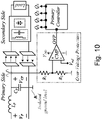
- an Over-Voltage Protection (OVP) mechanism has been implemented, as illustrated by Fig. 10 .
- the voltage V CP is sensed and scaled down by a high-resistance divider network to voltage levels suitable for the comparator operation.
- the scaling of V CP and the value of the reference voltage, V ref are determined according to the highest voltage allowed across the capacitor C P , i.e., across the coupling plates.
- the comparator output is fed to the primary's controller disabling the gate drive signals (Q 1 -Q 4 ), and as a result the system is turned off, until it is being reset. This also allows avoiding undesired safety concerns due to arcing and high electric fields around the coupling plates.
- the coupling plates have been designed symmetrically, such that each plate is 30x30cm.
- the full-bridge inverter has been implemented with GaN power devices operable in several MHz. The overall nominal operating conditions and parameters of the experimental prototype are summarized in Table I.
- the first step of the experimental validation has been carried out by characterizing the inductance of the variable inductor, and the resulting operating frequency of the CPT prototype as a function of the bias current.
- Fig. 11 shows the measured results for varying the bias current in the range of 0 to 2 A. It can be seen that in the vicinity of the nominal operating conditions the inductance and operating frequency f 0 are approximately 75 ⁇ H and 1.2 MHz, respectively, for a bias current of 0.5 A.
- Fig. 12B and Fig. 12C show zoomed-in views of the tuning process with the waveforms of the switching nodes voltages and resonant currents upon initialization and the end ( Fig. 12C ) of the tuning process.
- the switching frequency increases from 892 kHz to 1.2 MHz.
- the output parameters ( I S and V S ) also increase by more than 2.5 times, delivering more energy to the load, while the transfer efficiency has improved considerably (over 25% improvement).
- the primary current I P is slightly lagging the primary voltage V P , which is the necessary condition to enable soft-switching operation.
- the experimental prototype has been also tested for a target power of 10 W over various output load resistances, whereas the coupling capacitance C M ⁇ 20 pF, as shown in Fig. 13A .
- a virtually constant power delivery is obtained throughout the load range.
- the coupling capacitance has been varied to demonstrate the closed-loop operation under variations in the distance or displacement of the coupling plates.
Landscapes
- Engineering & Computer Science (AREA)
- Power Engineering (AREA)
- Computer Networks & Wireless Communication (AREA)
- Inverter Devices (AREA)
- Transceivers (AREA)
- Dc-Dc Converters (AREA)
Claims (15)
- Système de transfert d'énergie capacitive (CPT) sans fil contrôlé, basé sur des réseaux adaptatifs, comprenant :a) un côté transmetteur d'énergie primaire pour la transmission sans fil d'une puissance à un côté récepteur d'énergie secondaire via des plaques de couplage présentant une capacité mutuelle CM , ledit côté primaire comprenant :a.1) une source d'énergie connectée à un étage de puissance fonctionnant à une fréquence de commutation fsw déterminée ;a.2) un réseau adaptatif primaire constitué d'un circuit résonnant primaire avec une inductance primaire variable contrôlée par polarisation, branchée en série à ladite capacité mutuelle CM et d'un condensateur branché en parallèle à ladite capacité mutuelle CM pour la régulation du courant s'écoulent dudit côté primaire via ladite capacité mutuelle CM ,a.3) un contrôleur primaire constitué de :a.3.1) une première boucle de contrôle permettant d'ajuster la fréquence de commutation fsw afin de compenser les changements dans l'impédance dudit réseau adaptatif primaire lorsque ladite capacité mutuelle CM varie ;a.3.2) une deuxième boucle de contrôle permettant d'ajuster la fréquence de résonance dudit circuit résonnant primaire afin de suivre la fréquence de commutation fsw en appliquant une polarisation appropriée à ladite inductance primaire et en modifiant ladite fréquence de résonance dudit circuit résonnant primaire ;ledit côté secondaire comprenant :b.l) un circuit redresseur connecté à une charge et fonctionnant à la fréquence de résonance dudit circuit résonnant primaire ;b.2) un deuxième circuit adaptatif connecté entre ladite capacité mutuelle CM et ledit circuit redresseur et constitué d'un circuit résonnant secondaire avec une inductance secondaire variable contrôlée par polarisation, branchée en série à ladite capacité mutuelle CM et un condensateur parallèle branché en parallèle à ladite capacité mutuelle CM afin d'adapter l'impédance dudit réseau adaptatif secondaire ;b.3) un contrôleur secondaire constitué de :
b.3.1) une boucle de contrôle permettant d'ajuster l'impédance dudit réseau adaptatif secondaire afin d'adapter la fréquence de résonance dudit circuit résonnant primaire en appliquant une polarisation appropriée à ladite inductance secondaire. - Système selon la revendication 1, dans lequel la fréquence de commutation est synthétisée afin de suivre de manière continue la fréquence de résonance du côté primaire, en réponse aux variations des paramètres du système, dans lequel ladite synthèse de la fréquence de commutation est facilitée par DPLL.
- Système selon la revendication 1, dans lequel l'apport d'énergie du côté primaire au côté secondaire est syntonisé de manière adaptative afin de respecter les conditions de puissance soit au niveau des bornes des plaques de couplage soit au niveau des bornes de sortie, de façon à ce que ledit apport d'énergie soit désengagé des interactions croisées entre les côtés de transmission et de réception et des variations des circuits électriques et du support capacitif.
- Système selon la revendication 1, dans lequel l'apport d'énergie du côté primaire au côté secondaire est syntonisé de manière adaptative en ajustant la fréquence de fonctionnement et en faisant varier la valeur d'un ou plusieurs composants réactifs.
- Système selon la revendication 1, dans lequel le réseau adaptatif comprend une inductance ou capacitance contrôlée par polarisation ou contrôlée par une commande, ladite inductance ou capacitance contrôlée variant de manière continue ou par segments.
- Système selon la revendication 1, dans lequel la fréquence de résonance des circuits résonnants primaire et secondaire est ajustée en modifiant les valeurs des inductances ou des condensateurs parallèles ou les deux.
- Système selon la revendication 1, dans lequel la fréquence de commande suit la fréquence de résonance à la volée et l'énergie transmise est régulée par les caractéristiques du circuit résonnant afin d'obtenir un courant constant ou régulé délivré du côté primaire au côté secondaire.
- Système selon la revendication 1, dans lequel le réseau résonnant comprend une pluralité d'inductances et de condensateurs branchés soit en série soit en parallèle, ou une combinaison des deux branchements.
- Système selon la revendication 1, dans lequel le réseau résonnant comprend, dans chaque côté, deux composants variables ou plus.
- Système selon la revendication 1, dans lequel la largeur de bande de la première boucle de contrôle est la largeur de bande la plus élevée afin d'obtenir la réponse la plus rapide, la largeur de bande de la boucle de contrôle du côté secondaire étant inférieure à la largeur de bande de la première boucle de contrôle et la largeur de bande de la deuxième boucle de contrôle étant la largeur de bande la plus faible.
- Système selon la revendication 1, dans lequel le contrôleur de polarisation des inductances variables est constitué soit d'un régulateur linéaire soit d'un convertisseur abaisseur de tension et est régulé par une boucle de courant fermé interne.
- Système selon la revendication 1, dans lequel les boucles de contrôle diffèrent par leurs largeurs de bande.
- Système selon la revendication 1, dans lequel le signal transmis au niveau des bornes de sortie du côté primaire est modulé pour la transmission de l'énergie à une pluralité de charges, chacune correspondant à un côté secondaire, de façon à ce que chaque charge reçoive l'énergie transmise à une fréquence différente.
- Système selon la revendication 1, dans lequel une boucle de retour optionnelle est employée pour faciliter la régulation directe des caractéristiques de sortie par l'intermédiaire d'une communication de retour du côté secondaire vers le côté primaire, dans lequel ladite boucle de retour optionnelle ajuste le signal transmis par le côté primaire jusqu'à ce qu'un signal transmis souhaité soit obtenu.
- Procédé de contrôle d'un transfert d'énergie dans un système de transfert d'énergie capacitive (CPT), dans lequel ce système comprend un côté primaire et un côté secondaire, le côté primaire comprenant un réseau adaptatif primaire comprenant une inductance Lp et un condensateur Cp et le côté secondaire comprend un réseau adaptatif secondaire comprenant une inductance Ls et un condensateur Cs, ce procédé comprenant :a) lors de l'initiation de la syntonisation des réseaux adaptatifs primaire et secondaire, la détermination de la fréquence de commutation fsw et des valeurs d'inductance des inductances primaire et secondaire variables en tant qu'ensemble par défaut de valeur pré-chargées ;b) la syntonisation de la fréquence de commutation de la commande primaire par une première boucle de contrôle ;c) la détection d'une différence de phase entre les signaux Vp, c'est-à-dire la tension d'entrée du système au niveau du côté primaire, et VCP, c'est-à-dire la tension aux bornes de Cp, et le maintien d'un angle de phase de 90° entre VP et VCP à tout moment ;d) lorsque la différence de phase détectée entre lesdits signaux n'est pas égale à 90°, la génération d'un signal d'erreur afin de créer une nouvelle fréquence de commutation, jusqu'à ce que ladite fréquence de commutation soit égale à la fréquence de résonance ;e) la détection d'une différence de phase entre Vs, c'est-à-dire la tension de sortie du système au niveau du côté secondaire, et Vcs, c'est-à-dire la tension aux bornes de Cs, et le maintien de ladite différence de phase à 90° ;f) l'ajustement de la valeur d'inductance Ls du côté secondaire afin de syntoniser le réseau adaptatif secondaire, en fonction de la fréquence de commutation fsw du côté primaire ;g) la génération d'un signal de correction afin d'ajuster la valeur d'inductance Ls jusqu'à ce que le réseau soit en résonance (jusqu'à fsw = fo) et la différence de phase entre les signaux Vs et Vcs soit égale à 90° ;h) la génération d'un signal de correction qui ajuste l'inductance LP par l'intermédiaire d'un enroulement de polarisation jusqu'à ce que le courant souhaité soit obtenu.
Applications Claiming Priority (2)
| Application Number | Priority Date | Filing Date | Title |
|---|---|---|---|
| US201762582328P | 2017-11-07 | 2017-11-07 | |
| PCT/IL2018/051183 WO2019092701A1 (fr) | 2017-11-07 | 2018-11-06 | Transfert de puissance sans fil capacitif au moyen de réseaux d'adaptation adaptatifs |
Publications (3)
| Publication Number | Publication Date |
|---|---|
| EP3707801A1 EP3707801A1 (fr) | 2020-09-16 |
| EP3707801A4 EP3707801A4 (fr) | 2021-08-25 |
| EP3707801B1 true EP3707801B1 (fr) | 2022-10-05 |
Family
ID=66439097
Family Applications (1)
| Application Number | Title | Priority Date | Filing Date |
|---|---|---|---|
| EP18875280.2A Active EP3707801B1 (fr) | 2017-11-07 | 2018-11-06 | Transfert de puissance sans fil capacitif au moyen de réseaux d'adaptation adaptatifs |
Country Status (5)
| Country | Link |
|---|---|
| US (1) | US10965156B2 (fr) |
| EP (1) | EP3707801B1 (fr) |
| CN (1) | CN111279577B (fr) |
| ES (1) | ES2930112T3 (fr) |
| WO (1) | WO2019092701A1 (fr) |
Families Citing this family (26)
| Publication number | Priority date | Publication date | Assignee | Title |
|---|---|---|---|---|
| US12057711B2 (en) * | 2018-02-19 | 2024-08-06 | Naptilus Technology Lab, S.L. | Tuner and rectifier circuit for wireless power receiver |
| CN111937285B (zh) * | 2018-03-28 | 2023-11-17 | 株式会社村田制作所 | 电压转换器 |
| KR102544616B1 (ko) * | 2018-04-10 | 2023-06-19 | 삼성전자주식회사 | 무선 전력 전송 시스템 및 그 시스템을 포함하는 디스플레이 장치 |
| US11264835B2 (en) * | 2019-05-15 | 2022-03-01 | Qatar University | Inductive-capacitive network circuit for capacitive power transfer |
| FR3097701B1 (fr) * | 2019-06-24 | 2022-01-21 | Valeo Systemes De Controle Moteur | Circuit électrique pour charge d’une source de tension continue |
| US11079822B2 (en) * | 2019-06-28 | 2021-08-03 | Western Digital Technologies, Inc. | Integrated power and thermal management in non-volatile memory |
| CN110707832B (zh) * | 2019-10-15 | 2021-10-29 | 浙江大学 | 一种非完全补偿的无线电能传输系统 |
| CN110829624A (zh) * | 2019-10-18 | 2020-02-21 | 成都斯普奥汀科技有限公司 | 一种用于磁共振无线充电的自适应匹配系统 |
| CN111541425B (zh) * | 2020-04-11 | 2023-04-07 | 复旦大学 | 一种基于耦合传输线的阻抗匹配电路 |
| CN112242752B (zh) * | 2020-09-07 | 2022-07-05 | 合肥有感科技有限责任公司 | 无线充电系统工作频率的选调方法 |
| CN111817451B (zh) * | 2020-09-07 | 2021-02-02 | 北京有感科技有限责任公司 | 无线充电系统 |
| US11175319B1 (en) * | 2020-09-18 | 2021-11-16 | Stmicroelectronics Asia Pacific Pte Ltd | High accuracy low temperature drift high-side current sensing hardware and method |
| WO2022075092A1 (fr) * | 2020-10-09 | 2022-04-14 | パナソニックIpマネジメント株式会社 | Système de transmission d'énergie sans fil, dispositif de transmission d'énergie, et corps mobile |
| CN112701803B (zh) * | 2021-01-19 | 2022-12-02 | 华中科技大学 | 基于fsk并联注入通信的无线能量信号同步传输系统 |
| CN113054752B (zh) * | 2021-03-18 | 2022-04-29 | 中国人民解放军海军工程大学 | 一种恒压输出的电场耦合无线电能传输系统参数设计方法 |
| CN113078739B (zh) * | 2021-03-18 | 2022-07-19 | 中国人民解放军海军工程大学 | 一种恒流输出的电场耦合无线电能传输系统参数设计方法 |
| CN113037230B (zh) * | 2021-03-22 | 2022-06-24 | 湖南大学 | 电声换能系统阻抗匹配控制方法及系统 |
| CN113346630A (zh) * | 2021-05-10 | 2021-09-03 | 伏达半导体(合肥)有限公司 | 通信设备、系统及其方法 |
| CN113567759B (zh) * | 2021-07-20 | 2022-05-13 | 南京航空航天大学 | 基于阻抗稳定边界的电力电子装置参数优化方法及系统 |
| CN117652075A (zh) | 2021-09-29 | 2024-03-05 | 三星电子株式会社 | 包括用于减少谐波的尺寸减小的逆变器的无线电力发送器 |
| CN113972749B (zh) * | 2021-10-27 | 2023-08-11 | 西南交通大学 | 多端口电容式耦合机构及解耦型补偿拓扑的cpt系统 |
| WO2023128440A1 (fr) * | 2021-12-27 | 2023-07-06 | 삼성전자 주식회사 | Dispositif et procédé d'émission de tension de taille constante dans un système de communication sans fil |
| CN115459585B (zh) * | 2022-09-13 | 2024-09-20 | 浙江大学 | 一种基于电磁干扰模型的变流器箱体接地设计方法 |
| CN115648959B (zh) * | 2022-10-26 | 2024-06-18 | 西南交通大学 | 轨道交通非接触式供电系统 |
| WO2024166114A1 (fr) * | 2023-02-08 | 2024-08-15 | Remote Energy Ltd. | Système auto-oscillant pour transmission d'énergie sans fil et son procédé de mise en oeuvre |
| WO2024176240A1 (fr) * | 2023-02-26 | 2024-08-29 | Remote Energy Ltd. | Procédé et appareil de transmission d'énergie sans fil capacitive |
Family Cites Families (8)
| Publication number | Priority date | Publication date | Assignee | Title |
|---|---|---|---|---|
| GB2511448B (en) | 2011-11-24 | 2017-10-04 | Murata Manufacturing Co | Power transmission device and power transmission control method |
| KR101905783B1 (ko) * | 2012-04-05 | 2018-12-05 | 엘지이노텍 주식회사 | 임피던스 정합 장치 |
| US9276440B2 (en) * | 2012-09-07 | 2016-03-01 | WIPQTUS Inc. | Multi-mode multi-coupling multi-protocol ubiquitous wireless power transmitter |
| WO2014112639A1 (fr) * | 2013-01-21 | 2014-07-24 | 株式会社村田製作所 | Système d'émission de puissance |
| US20170005532A1 (en) * | 2013-12-26 | 2017-01-05 | Mitsubishi Electric Engineering Company, Limited | Automatic matching circuit for high frequency rectification circuit |
| WO2016161280A1 (fr) * | 2015-04-01 | 2016-10-06 | The Regents Of The University Of Michigan | Topologie à compensation lclc à deux côtés pour un transfert d'énergie capacitive |
| CA2985091C (fr) * | 2015-05-04 | 2023-09-26 | The Regents Of The University Of Colorado, A Body Corporate | Transfert d'energie sans fil |
| CN106787253B (zh) * | 2017-03-11 | 2019-04-09 | 重庆大学 | 基于t-π复合谐振网络ecpt系统及其参数设计方法 |
-
2018
- 2018-11-06 US US16/651,225 patent/US10965156B2/en active Active
- 2018-11-06 EP EP18875280.2A patent/EP3707801B1/fr active Active
- 2018-11-06 WO PCT/IL2018/051183 patent/WO2019092701A1/fr unknown
- 2018-11-06 CN CN201880063140.XA patent/CN111279577B/zh active Active
- 2018-11-06 ES ES18875280T patent/ES2930112T3/es active Active
Also Published As
| Publication number | Publication date |
|---|---|
| US20200287413A1 (en) | 2020-09-10 |
| EP3707801A4 (fr) | 2021-08-25 |
| EP3707801A1 (fr) | 2020-09-16 |
| WO2019092701A1 (fr) | 2019-05-16 |
| CN111279577B (zh) | 2023-10-17 |
| CN111279577A (zh) | 2020-06-12 |
| ES2930112T3 (es) | 2022-12-07 |
| US10965156B2 (en) | 2021-03-30 |
Similar Documents
| Publication | Publication Date | Title |
|---|---|---|
| EP3707801B1 (fr) | Transfert de puissance sans fil capacitif au moyen de réseaux d'adaptation adaptatifs | |
| Abramov et al. | Multi-loop control for power transfer regulation in capacitive wireless systems by means of variable matching networks | |
| US11349342B2 (en) | Voltage regulation in wireless power receivers | |
| JP6489212B2 (ja) | 固定チューニングおよび電力制限機能を有する可変距離ワイヤレス給電システム | |
| US10103578B2 (en) | Power supply device, integrated circuit, energy transmitter and impedance matching method | |
| US9985442B2 (en) | Wireless power transfer receiver having closed loop voltage control | |
| US9899880B2 (en) | Power receiver, resonance-type contactless power supply and control method therefor | |
| US10923958B2 (en) | Power transmitter, resonance-type contactless power supply and control method thereof | |
| EP3453100A1 (fr) | Procédés et appareil d'adaptation d'impédance par régulation de tension | |
| WO2012085119A2 (fr) | Récepteur de puissance sans fil pour recevoir un signal de puissance sur un couplage inductif, et amélioration du procédé de mise en œuvre d'un récepteur de puissance sans fil | |
| US12057711B2 (en) | Tuner and rectifier circuit for wireless power receiver | |
| Pham et al. | Active rectifier design and synchronization control for 6.78 MHz wireless power transfer | |
| Abramov et al. | Regulated power transfer using self-tuned networks for capacitive wireless systems | |
| CN110535343B (zh) | 用于谐振电路的控制器和控制方法以及直流-直流转换器 | |
| EP3528365B1 (fr) | Appareil de syntoniseur et de redresseur pour récepteur de transfert de puissance sans fil | |
| US20230327650A1 (en) | Continuously variable active reactance systems and methods | |
| US11462947B2 (en) | Wireless power receiver having transfer optimization and method thereof | |
| Lu et al. | Wireless Power Transfer Systems | |
| Nikiforidis et al. | Primary-side Output Regulation Principles in Dynamic Multi-MHz Inductive Power Transfer Systems and Isolated DC/DC Converters |
Legal Events
| Date | Code | Title | Description |
|---|---|---|---|
| STAA | Information on the status of an ep patent application or granted ep patent |
Free format text: STATUS: THE INTERNATIONAL PUBLICATION HAS BEEN MADE |
|
| PUAI | Public reference made under article 153(3) epc to a published international application that has entered the european phase |
Free format text: ORIGINAL CODE: 0009012 |
|
| STAA | Information on the status of an ep patent application or granted ep patent |
Free format text: STATUS: REQUEST FOR EXAMINATION WAS MADE |
|
| 17P | Request for examination filed |
Effective date: 20200326 |
|
| AK | Designated contracting states |
Kind code of ref document: A1 Designated state(s): AL AT BE BG CH CY CZ DE DK EE ES FI FR GB GR HR HU IE IS IT LI LT LU LV MC MK MT NL NO PL PT RO RS SE SI SK SM TR |
|
| AX | Request for extension of the european patent |
Extension state: BA ME |
|
| DAV | Request for validation of the european patent (deleted) | ||
| DAX | Request for extension of the european patent (deleted) | ||
| A4 | Supplementary search report drawn up and despatched |
Effective date: 20210726 |
|
| RIC1 | Information provided on ipc code assigned before grant |
Ipc: H02J 50/05 20160101AFI20210720BHEP Ipc: H02J 50/90 20160101ALI20210720BHEP Ipc: H02J 7/04 20060101ALI20210720BHEP |
|
| RIC1 | Information provided on ipc code assigned before grant |
Ipc: H02M 3/335 20060101ALI20220323BHEP Ipc: H02J 7/04 20060101ALI20220323BHEP Ipc: H02J 50/90 20160101ALI20220323BHEP Ipc: H02J 50/05 20160101AFI20220323BHEP |
|
| GRAP | Despatch of communication of intention to grant a patent |
Free format text: ORIGINAL CODE: EPIDOSNIGR1 |
|
| STAA | Information on the status of an ep patent application or granted ep patent |
Free format text: STATUS: GRANT OF PATENT IS INTENDED |
|
| INTG | Intention to grant announced |
Effective date: 20220516 |
|
| GRAS | Grant fee paid |
Free format text: ORIGINAL CODE: EPIDOSNIGR3 |
|
| GRAA | (expected) grant |
Free format text: ORIGINAL CODE: 0009210 |
|
| STAA | Information on the status of an ep patent application or granted ep patent |
Free format text: STATUS: THE PATENT HAS BEEN GRANTED |
|
| AK | Designated contracting states |
Kind code of ref document: B1 Designated state(s): AL AT BE BG CH CY CZ DE DK EE ES FI FR GB GR HR HU IE IS IT LI LT LU LV MC MK MT NL NO PL PT RO RS SE SI SK SM TR |
|
| REG | Reference to a national code |
Ref country code: GB Ref legal event code: FG4D |
|
| REG | Reference to a national code |
Ref country code: CH Ref legal event code: EP |
|
| REG | Reference to a national code |
Ref country code: AT Ref legal event code: REF Ref document number: 1523372 Country of ref document: AT Kind code of ref document: T Effective date: 20221015 |
|
| REG | Reference to a national code |
Ref country code: IE Ref legal event code: FG4D |
|
| REG | Reference to a national code |
Ref country code: DE Ref legal event code: R096 Ref document number: 602018041546 Country of ref document: DE |
|
| REG | Reference to a national code |
Ref country code: ES Ref legal event code: FG2A Ref document number: 2930112 Country of ref document: ES Kind code of ref document: T3 Effective date: 20221207 |
|
| REG | Reference to a national code |
Ref country code: LT Ref legal event code: MG9D |
|
| REG | Reference to a national code |
Ref country code: NL Ref legal event code: MP Effective date: 20221005 |
|
| REG | Reference to a national code |
Ref country code: AT Ref legal event code: MK05 Ref document number: 1523372 Country of ref document: AT Kind code of ref document: T Effective date: 20221005 |
|
| PG25 | Lapsed in a contracting state [announced via postgrant information from national office to epo] |
Ref country code: NL Free format text: LAPSE BECAUSE OF FAILURE TO SUBMIT A TRANSLATION OF THE DESCRIPTION OR TO PAY THE FEE WITHIN THE PRESCRIBED TIME-LIMIT Effective date: 20221005 |
|
| PG25 | Lapsed in a contracting state [announced via postgrant information from national office to epo] |
Ref country code: SE Free format text: LAPSE BECAUSE OF FAILURE TO SUBMIT A TRANSLATION OF THE DESCRIPTION OR TO PAY THE FEE WITHIN THE PRESCRIBED TIME-LIMIT Effective date: 20221005 Ref country code: PT Free format text: LAPSE BECAUSE OF FAILURE TO SUBMIT A TRANSLATION OF THE DESCRIPTION OR TO PAY THE FEE WITHIN THE PRESCRIBED TIME-LIMIT Effective date: 20230206 Ref country code: NO Free format text: LAPSE BECAUSE OF FAILURE TO SUBMIT A TRANSLATION OF THE DESCRIPTION OR TO PAY THE FEE WITHIN THE PRESCRIBED TIME-LIMIT Effective date: 20230105 Ref country code: LT Free format text: LAPSE BECAUSE OF FAILURE TO SUBMIT A TRANSLATION OF THE DESCRIPTION OR TO PAY THE FEE WITHIN THE PRESCRIBED TIME-LIMIT Effective date: 20221005 Ref country code: FI Free format text: LAPSE BECAUSE OF FAILURE TO SUBMIT A TRANSLATION OF THE DESCRIPTION OR TO PAY THE FEE WITHIN THE PRESCRIBED TIME-LIMIT Effective date: 20221005 Ref country code: AT Free format text: LAPSE BECAUSE OF FAILURE TO SUBMIT A TRANSLATION OF THE DESCRIPTION OR TO PAY THE FEE WITHIN THE PRESCRIBED TIME-LIMIT Effective date: 20221005 |
|
| PG25 | Lapsed in a contracting state [announced via postgrant information from national office to epo] |
Ref country code: RS Free format text: LAPSE BECAUSE OF FAILURE TO SUBMIT A TRANSLATION OF THE DESCRIPTION OR TO PAY THE FEE WITHIN THE PRESCRIBED TIME-LIMIT Effective date: 20221005 Ref country code: PL Free format text: LAPSE BECAUSE OF FAILURE TO SUBMIT A TRANSLATION OF THE DESCRIPTION OR TO PAY THE FEE WITHIN THE PRESCRIBED TIME-LIMIT Effective date: 20221005 Ref country code: LV Free format text: LAPSE BECAUSE OF FAILURE TO SUBMIT A TRANSLATION OF THE DESCRIPTION OR TO PAY THE FEE WITHIN THE PRESCRIBED TIME-LIMIT Effective date: 20221005 Ref country code: IS Free format text: LAPSE BECAUSE OF FAILURE TO SUBMIT A TRANSLATION OF THE DESCRIPTION OR TO PAY THE FEE WITHIN THE PRESCRIBED TIME-LIMIT Effective date: 20230205 Ref country code: HR Free format text: LAPSE BECAUSE OF FAILURE TO SUBMIT A TRANSLATION OF THE DESCRIPTION OR TO PAY THE FEE WITHIN THE PRESCRIBED TIME-LIMIT Effective date: 20221005 Ref country code: GR Free format text: LAPSE BECAUSE OF FAILURE TO SUBMIT A TRANSLATION OF THE DESCRIPTION OR TO PAY THE FEE WITHIN THE PRESCRIBED TIME-LIMIT Effective date: 20230106 |
|
| P01 | Opt-out of the competence of the unified patent court (upc) registered |
Effective date: 20230511 |
|
| REG | Reference to a national code |
Ref country code: CH Ref legal event code: PL |
|
| REG | Reference to a national code |
Ref country code: DE Ref legal event code: R097 Ref document number: 602018041546 Country of ref document: DE |
|
| REG | Reference to a national code |
Ref country code: BE Ref legal event code: MM Effective date: 20221130 |
|
| PG25 | Lapsed in a contracting state [announced via postgrant information from national office to epo] |
Ref country code: SM Free format text: LAPSE BECAUSE OF FAILURE TO SUBMIT A TRANSLATION OF THE DESCRIPTION OR TO PAY THE FEE WITHIN THE PRESCRIBED TIME-LIMIT Effective date: 20221005 Ref country code: RO Free format text: LAPSE BECAUSE OF FAILURE TO SUBMIT A TRANSLATION OF THE DESCRIPTION OR TO PAY THE FEE WITHIN THE PRESCRIBED TIME-LIMIT Effective date: 20221005 Ref country code: MC Free format text: LAPSE BECAUSE OF FAILURE TO SUBMIT A TRANSLATION OF THE DESCRIPTION OR TO PAY THE FEE WITHIN THE PRESCRIBED TIME-LIMIT Effective date: 20221005 Ref country code: LI Free format text: LAPSE BECAUSE OF NON-PAYMENT OF DUE FEES Effective date: 20221130 Ref country code: EE Free format text: LAPSE BECAUSE OF FAILURE TO SUBMIT A TRANSLATION OF THE DESCRIPTION OR TO PAY THE FEE WITHIN THE PRESCRIBED TIME-LIMIT Effective date: 20221005 Ref country code: DK Free format text: LAPSE BECAUSE OF FAILURE TO SUBMIT A TRANSLATION OF THE DESCRIPTION OR TO PAY THE FEE WITHIN THE PRESCRIBED TIME-LIMIT Effective date: 20221005 Ref country code: CZ Free format text: LAPSE BECAUSE OF FAILURE TO SUBMIT A TRANSLATION OF THE DESCRIPTION OR TO PAY THE FEE WITHIN THE PRESCRIBED TIME-LIMIT Effective date: 20221005 Ref country code: CH Free format text: LAPSE BECAUSE OF NON-PAYMENT OF DUE FEES Effective date: 20221130 |
|
| PLBE | No opposition filed within time limit |
Free format text: ORIGINAL CODE: 0009261 |
|
| STAA | Information on the status of an ep patent application or granted ep patent |
Free format text: STATUS: NO OPPOSITION FILED WITHIN TIME LIMIT |
|
| PG25 | Lapsed in a contracting state [announced via postgrant information from national office to epo] |
Ref country code: SK Free format text: LAPSE BECAUSE OF FAILURE TO SUBMIT A TRANSLATION OF THE DESCRIPTION OR TO PAY THE FEE WITHIN THE PRESCRIBED TIME-LIMIT Effective date: 20221005 Ref country code: LU Free format text: LAPSE BECAUSE OF NON-PAYMENT OF DUE FEES Effective date: 20221106 Ref country code: AL Free format text: LAPSE BECAUSE OF FAILURE TO SUBMIT A TRANSLATION OF THE DESCRIPTION OR TO PAY THE FEE WITHIN THE PRESCRIBED TIME-LIMIT Effective date: 20221005 |
|
| 26N | No opposition filed |
Effective date: 20230706 |
|
| PG25 | Lapsed in a contracting state [announced via postgrant information from national office to epo] |
Ref country code: IE Free format text: LAPSE BECAUSE OF NON-PAYMENT OF DUE FEES Effective date: 20221106 |
|
| PG25 | Lapsed in a contracting state [announced via postgrant information from national office to epo] |
Ref country code: SI Free format text: LAPSE BECAUSE OF FAILURE TO SUBMIT A TRANSLATION OF THE DESCRIPTION OR TO PAY THE FEE WITHIN THE PRESCRIBED TIME-LIMIT Effective date: 20221005 Ref country code: BE Free format text: LAPSE BECAUSE OF NON-PAYMENT OF DUE FEES Effective date: 20221130 |
|
| PGFP | Annual fee paid to national office [announced via postgrant information from national office to epo] |
Ref country code: GB Payment date: 20231121 Year of fee payment: 6 |
|
| PGFP | Annual fee paid to national office [announced via postgrant information from national office to epo] |
Ref country code: ES Payment date: 20231219 Year of fee payment: 6 |
|
| PGFP | Annual fee paid to national office [announced via postgrant information from national office to epo] |
Ref country code: IT Payment date: 20231124 Year of fee payment: 6 Ref country code: FR Payment date: 20231123 Year of fee payment: 6 Ref country code: DE Payment date: 20231127 Year of fee payment: 6 |
|
| PG25 | Lapsed in a contracting state [announced via postgrant information from national office to epo] |
Ref country code: CY Free format text: LAPSE BECAUSE OF FAILURE TO SUBMIT A TRANSLATION OF THE DESCRIPTION OR TO PAY THE FEE WITHIN THE PRESCRIBED TIME-LIMIT Effective date: 20221005 |
|
| PG25 | Lapsed in a contracting state [announced via postgrant information from national office to epo] |
Ref country code: MK Free format text: LAPSE BECAUSE OF FAILURE TO SUBMIT A TRANSLATION OF THE DESCRIPTION OR TO PAY THE FEE WITHIN THE PRESCRIBED TIME-LIMIT Effective date: 20221005 Ref country code: HU Free format text: LAPSE BECAUSE OF FAILURE TO SUBMIT A TRANSLATION OF THE DESCRIPTION OR TO PAY THE FEE WITHIN THE PRESCRIBED TIME-LIMIT; INVALID AB INITIO Effective date: 20181106 |
|
| PG25 | Lapsed in a contracting state [announced via postgrant information from national office to epo] |
Ref country code: BG Free format text: LAPSE BECAUSE OF FAILURE TO SUBMIT A TRANSLATION OF THE DESCRIPTION OR TO PAY THE FEE WITHIN THE PRESCRIBED TIME-LIMIT Effective date: 20221005 |
|
| PG25 | Lapsed in a contracting state [announced via postgrant information from national office to epo] |
Ref country code: MT Free format text: LAPSE BECAUSE OF FAILURE TO SUBMIT A TRANSLATION OF THE DESCRIPTION OR TO PAY THE FEE WITHIN THE PRESCRIBED TIME-LIMIT Effective date: 20221005 |