EP3707750B1 - Optoelektronische module mit verriegelungsanordnungen und verfahren zu ihrer herstellung - Google Patents
Optoelektronische module mit verriegelungsanordnungen und verfahren zu ihrer herstellung Download PDFInfo
- Publication number
- EP3707750B1 EP3707750B1 EP18875232.3A EP18875232A EP3707750B1 EP 3707750 B1 EP3707750 B1 EP 3707750B1 EP 18875232 A EP18875232 A EP 18875232A EP 3707750 B1 EP3707750 B1 EP 3707750B1
- Authority
- EP
- European Patent Office
- Prior art keywords
- overmold
- assembly
- optical element
- housing
- tool
- Prior art date
- Legal status (The legal status is an assumption and is not a legal conclusion. Google has not performed a legal analysis and makes no representation as to the accuracy of the status listed.)
- Active
Links
Images


Classifications
-
- G—PHYSICS
- G02—OPTICS
- G02B—OPTICAL ELEMENTS, SYSTEMS OR APPARATUS
- G02B7/00—Mountings, adjusting means, or light-tight connections, for optical elements
- G02B7/02—Mountings, adjusting means, or light-tight connections, for optical elements for lenses
-
- H—ELECTRICITY
- H10—SEMICONDUCTOR DEVICES; ELECTRIC SOLID-STATE DEVICES NOT OTHERWISE PROVIDED FOR
- H10F—INORGANIC SEMICONDUCTOR DEVICES SENSITIVE TO INFRARED RADIATION, LIGHT, ELECTROMAGNETIC RADIATION OF SHORTER WAVELENGTH OR CORPUSCULAR RADIATION
- H10F39/00—Integrated devices, or assemblies of multiple devices, comprising at least one element covered by group H10F30/00, e.g. radiation detectors comprising photodiode arrays
- H10F39/80—Constructional details of image sensors
- H10F39/804—Containers or encapsulations
-
- H—ELECTRICITY
- H10—SEMICONDUCTOR DEVICES; ELECTRIC SOLID-STATE DEVICES NOT OTHERWISE PROVIDED FOR
- H10F—INORGANIC SEMICONDUCTOR DEVICES SENSITIVE TO INFRARED RADIATION, LIGHT, ELECTROMAGNETIC RADIATION OF SHORTER WAVELENGTH OR CORPUSCULAR RADIATION
- H10F77/00—Constructional details of devices covered by this subclass
- H10F77/40—Optical elements or arrangements
- H10F77/407—Optical elements or arrangements indirectly associated with the devices
-
- H—ELECTRICITY
- H10—SEMICONDUCTOR DEVICES; ELECTRIC SOLID-STATE DEVICES NOT OTHERWISE PROVIDED FOR
- H10F—INORGANIC SEMICONDUCTOR DEVICES SENSITIVE TO INFRARED RADIATION, LIGHT, ELECTROMAGNETIC RADIATION OF SHORTER WAVELENGTH OR CORPUSCULAR RADIATION
- H10F77/00—Constructional details of devices covered by this subclass
- H10F77/50—Encapsulations or containers
-
- H—ELECTRICITY
- H10—SEMICONDUCTOR DEVICES; ELECTRIC SOLID-STATE DEVICES NOT OTHERWISE PROVIDED FOR
- H10H—INORGANIC LIGHT-EMITTING SEMICONDUCTOR DEVICES HAVING POTENTIAL BARRIERS
- H10H20/00—Individual inorganic light-emitting semiconductor devices having potential barriers, e.g. light-emitting diodes [LED]
- H10H20/80—Constructional details
- H10H20/85—Packages
- H10H20/8506—Containers
-
- H—ELECTRICITY
- H10—SEMICONDUCTOR DEVICES; ELECTRIC SOLID-STATE DEVICES NOT OTHERWISE PROVIDED FOR
- H10H—INORGANIC LIGHT-EMITTING SEMICONDUCTOR DEVICES HAVING POTENTIAL BARRIERS
- H10H20/00—Individual inorganic light-emitting semiconductor devices having potential barriers, e.g. light-emitting diodes [LED]
- H10H20/80—Constructional details
- H10H20/85—Packages
- H10H20/855—Optical field-shaping means, e.g. lenses
-
- H—ELECTRICITY
- H10—SEMICONDUCTOR DEVICES; ELECTRIC SOLID-STATE DEVICES NOT OTHERWISE PROVIDED FOR
- H10W—GENERIC PACKAGES, INTERCONNECTIONS, CONNECTORS OR OTHER CONSTRUCTIONAL DETAILS OF DEVICES COVERED BY CLASS H10
- H10W74/00—Encapsulations, e.g. protective coatings
- H10W74/10—Encapsulations, e.g. protective coatings characterised by their shape or disposition
- H10W74/111—Encapsulations, e.g. protective coatings characterised by their shape or disposition the semiconductor body being completely enclosed
- H10W74/114—Encapsulations, e.g. protective coatings characterised by their shape or disposition the semiconductor body being completely enclosed by a substrate and the encapsulations
-
- H—ELECTRICITY
- H10—SEMICONDUCTOR DEVICES; ELECTRIC SOLID-STATE DEVICES NOT OTHERWISE PROVIDED FOR
- H10W—GENERIC PACKAGES, INTERCONNECTIONS, CONNECTORS OR OTHER CONSTRUCTIONAL DETAILS OF DEVICES COVERED BY CLASS H10
- H10W74/00—Encapsulations, e.g. protective coatings
- H10W74/10—Encapsulations, e.g. protective coatings characterised by their shape or disposition
- H10W74/111—Encapsulations, e.g. protective coatings characterised by their shape or disposition the semiconductor body being completely enclosed
- H10W74/127—Encapsulations, e.g. protective coatings characterised by their shape or disposition the semiconductor body being completely enclosed characterised by arrangements for sealing or adhesion
-
- H—ELECTRICITY
- H10—SEMICONDUCTOR DEVICES; ELECTRIC SOLID-STATE DEVICES NOT OTHERWISE PROVIDED FOR
- H10W—GENERIC PACKAGES, INTERCONNECTIONS, CONNECTORS OR OTHER CONSTRUCTIONAL DETAILS OF DEVICES COVERED BY CLASS H10
- H10W76/00—Containers; Fillings or auxiliary members therefor; Seals
- H10W76/10—Containers or parts thereof
- H10W76/12—Containers or parts thereof characterised by their shape
-
- H—ELECTRICITY
- H10—SEMICONDUCTOR DEVICES; ELECTRIC SOLID-STATE DEVICES NOT OTHERWISE PROVIDED FOR
- H10H—INORGANIC LIGHT-EMITTING SEMICONDUCTOR DEVICES HAVING POTENTIAL BARRIERS
- H10H20/00—Individual inorganic light-emitting semiconductor devices having potential barriers, e.g. light-emitting diodes [LED]
- H10H20/01—Manufacture or treatment
- H10H20/036—Manufacture or treatment of packages
Definitions
- the present disclosure relates to optoelectronic modules having locking assemblies and methods for manufacturing such modules.
- An optoelectronic module such as a proximity sensor, a structured-light generator, a two- or three-dimensional imaging camera, or an ambient light sensor, typically includes an optical assembly mounted to an optoelectronic component, such as a light emitting diode, a photodiode, a laser diode, or an imaging sensor. Mounting (i.e., involving the alignment and joining of these components) can be a challenge. Moreover, the useful lifetime of an optoelectronic module can be significantly reduced when an optical assembly becomes misaligned relative to a corresponding optoelectronic component during normal use. Consequently, a need for optoelectronic modules with improved mounting technology, and their manufacture, is needed.
- an optoelectronic module includes an optical element assembly.
- the optical element assembly includes an optical element mounted within an optical element housing.
- the optoelectronic module further includes an overmold assembly.
- the overmold assembly includes an optoelectronic component mounted to a substrate via electrical connections.
- the optoelectronic component and electrical connections are encapsulated by an overmold and the overmold is laterally circumscribed by an overmold housing.
- the optical element assembly is mounted to the overmold assembly via a locking assembly such that lateral movement of the optical element assembly relative to the overmold assembly is substantially restrained.
- the present disclosure describes a method for manufacturing optoelectronic modules having locking assemblies.
- the method includes:
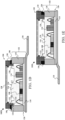
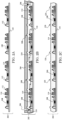
- FIG. 1A - FIG. 1E Examples of optoelectronic modules 100A - 100E are depicted in FIG. 1A - FIG. 1E , respectively.
- Each example optoelectronic module includes a locking assembly.
- the locking assembly improves mounting steps during manufacturing and increases the useful lifetime of the optoelectronic modules into which they are incorporated.
- Common reference numerals indicate similar features
- FIG. 1B - FIG. 1D depict optoelectronic modules according to the claimed invention.
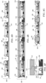
- FIG. 2A - FIG. 2K depict a method of manufacturing optoelectronic assemblies according to the claimed invention.
- Each of the optoelectronic modules 100A - 100E includes an overmold assembly 102 and an optical element assembly 104.
- the optical element assembly 104 can be mounted to the overmold assembly 102 via adhesive 106.
- the overmold assembly includes an optoelectronic component 108 mounted to a substrate 110 (e.g., printed circuit board) via electrical connections 112 (e.g., wire bonds). Still other electrical components 114 (e.g., capacitors) can be mounted to the substrate 110 via the electrical connections 112.
- the overmold assembly 102 further includes an overmold 116.
- the overmold 116 together with the substrate 110, encapsulates the optoelectronic component 108, the electrical connections 112, and any other electrical components 114 (if present).
- the overmold assembly 102 further includes an overmold housing 118 circumscribing the overmold 116.
- the overmold 116 can include overmold protrusions 120 and an overmold trench 122 both incorporated into a first side 124 of the overmold 116.
- the overmold assembly 102 can include a substrate trench 126 (i.e., a trench incised or otherwise formed in the substrate 110). When present, the overmold housing 118 can extend into the substrate trench 126.
- the substrate trench 126 can improve mechanical robustness of the optoelectronic modules 100A and/or can eliminate stray light from passing between the substrate 110 and the overmold housing 118.
- the first side 124 of the overmold 116 can include one or more optical elements.
- an optical element such as an optical filter, could be coated onto the first side 124.
- an optical element can be formed into the first side 124 of the overmold 116 as depicted din FIG. 1D .
- the optical element assembly 104 includes an optical element 128 mounted within an optical element housing 130.
- the optical element 128 can include a refractive lens, a diffractive lens, a microlens array, a diffuser, other diffractive elements, an optical filter (e.g., an infrared filter), or any combination of the aforementioned.
- the optical element assembly 104 further includes an optical element housing protrusion 132 extending form the optical element housing 130. Both the optical element housing 130 and the optical element housing 132 can be composed, at least partially, of cured epoxy. In some instances, the optical element housing protrusion 132 and the optical element housing 130 can be formed at the same time and can be materially contiguous, though they need not be.
- the overmold housing 118 can include a locking edge 134 configured to engage with the optical element housing protrusion 132 (as depicted in FIG. 1A - FIG. 1D ).
- the optoelectronic modules 100A - 100E can be mounted onto a flex cable 136 (not depicted in FIG. 1A - FIG. 1C for clarity).
- FIG. 2A - FIG. 2K depict an example of a method for manufacturing optoelectronic modules having locking assemblies, such as the optoelectronic modules 100A - 100E depicted in FIG. 1A - FIG. 1E , respectively.
- a wafer assembly 202 is constructed.
- the wafer assembly 202 can include various films and mounting components as would be apparent to a person of ordinary skill in the art.
- the wafer assembly 202 can be mounted to a vacuum chuck during various steps of the example manufacturing method.
- the wafer assembly 202 is constructed in part by mounting a plurality of optoelectronic components 108 to the substrate 110 via the electrical connections 112 as depicted in FIG. 2A .
- an overmold tool 204 is mounted to the wafer assembly 202.
- the overmold tool 204 includes a plurality of overmold tool channels 206 and a plurality of overmold tool trenches 206 as depicted in FIG. 2B .
- a formable overmold material 210 is introduced into the wafer assembly 202 via the plurality of overmold tool channels 206 such that the plurality of optoelectronic components 108 and electrical connections 112 (and in some instances other electrical components 114) are encapsulated and the plurality of overmold tool trenches 208 are at least partially filled with the formable overmold material 210 as further depicted in FIG. 2B .
- the formable overmold material 210 is then cured in a subsequent step with electromagnetic radiation (e.g., infrared or ultraviolet light) and/or thermal energy such that the formable overmold material 210 is substantially solid.
- the overmold tool 204 is then removed from the wafer assembly 202 in a subsequent step as depicted in FIG. 2C .
- the overmold 116 and substrate 110 are dice into such that a plurality of module trenches 212 is formed. In some instances, only the overmold 116 is diced into.
- a housing tool 214 is mounted to the wafer assembly 202.
- the housing tool 214 includes a plurality of housing tool channels 216 and a plurality of housing tool protrusions 218.
- a formable housing material 220 is introduced into the wafer assembly 202 via the plurality of housing tool channels 216 such that the module trenches 212 are at least partially filled with formable housing material 220 as depicted in FIG. 2E .
- FIG. 2F depicts an enlarged portion of FIG. 2E .
- the housing tool 214 does not make contact with the overmold protrusion 120. Rather, in some instances as depicted, the housing tool 214 (via the housing tool protrusion 218) makes contact with a small portion of the first side 124 of the overmold 116. In some instances, such a feature can prevent formable housing material 220 from migrating onto a large portion of the first side 124 of the overmold 116.
- the formable housing material 220 is cured with electromagnetic radiation and/or thermal energy such that the formable housing material 220 is substantially solid.
- the housing tool 214 is removed from the wafer assembly 202 as depicted in FIG. 2G .
- the substantially solid housing material is diced through along dicing lines 222 ( FIG. 2H ) generating a plurality of discrete overmold assemblies 202 as depicted in FIG. 2I .
- the overmold assembly 202 can be mounted to the felx cable 136; e.g., the optoelectronic component 108 can be electrically connected to the flex cable 136.
- the optical element assembly 104 is mounted to the overmold assembly 102 via adhesive and components of a locking assembly described above (e.g., overmold protrusions 120 and optical element protrusions 132).
- the adhesive can be partially or fully cured (e.g., with electromagnetic radiation and/or thermal energy), though need not be.
- the performance of the assembled optoelectronic module, 100C as depicted in FIG. 2K can be evaluated.
- the optoelectronic components 108 for example, can be activated via the flex cable 136 and tested for performance, efficiency and so on.
- Some of the aforementioned implementations describe a collection of steps for manufacturing pluralities of discrete optoelectronic modules. Various steps are described sequentially, though steps need not occur in the sequence described. Moreover, steps described sequentially may be carried out simultaneously. Further, the example steps described above can be repeated in some instances. Further, modifications can be made to the foregoing implementations, for example additional steps, such as steps involving the application of a releasing agent and steps involving oxygen plasma treatments, can be included in any of the aforementioned implementations.
- any of the above implementation can include an aperture (e.g., at least partially composed of black chrome) mounted or deposited onto any of the optical elements 128 (e.g., via photolithographic techniques, screen printing, and so forth). Still further, features described above in different implementations may be combined in the same implementations.
Landscapes
- Physics & Mathematics (AREA)
- General Physics & Mathematics (AREA)
- Optics & Photonics (AREA)
- Semiconductor Lasers (AREA)
- Light Receiving Elements (AREA)
- Led Device Packages (AREA)
- Optical Couplings Of Light Guides (AREA)
- Surface Acoustic Wave Elements And Circuit Networks Thereof (AREA)
- Photovoltaic Devices (AREA)
- Engineering & Computer Science (AREA)
- Microelectronics & Electronic Packaging (AREA)
Claims (11)
- Optoelektronisches Modul (100B, 100C, 100D) aufweisend:eine optische Element-Baugruppe (104) mit einem optischen Element (128), das in einem optischen Elementgehäuse (130) montiert ist;eine Umspritzung-Baugruppe (102), die Umspritzung-Baugruppe aufweisend:ein optoelektronisches Bauteil (108), das über elektrische Verbindungen (112) an einem Substrat (110) angebracht ist,eine Umspritzung (116), die das optoelektronische Bauteil und die elektrischen Verbindungen einkapselt, und ein Umspritzung-Gehäuse (118),das die Umspritzung seitlich umschließt;wobei die optische Element-Baugruppe über eine Verriegelungsbaugruppe (132, 134) an der Umspritzung-Baugruppe befestigt ist, so dass eine seitliche Bewegung der optischen Element-Baugruppe relativ zur Umspritzung-Baugruppe im Wesentlichen eingeschränkt ist,die Verriegelungsbaugruppe aufweisend:einen Vorsprung (132) des optischen Elementgehäuses, der sich von dem optischen Elementgehäuse erstreckt, wobei der Vorsprung des optischen Elementgehäuses in Kontakt mit einer ersten Seite (124) der Umspritzung ist;eine Verriegelungskante (134), die in das Umspritzung-Gehäuse eingearbeitet ist, wobei die Verriegelungskante benachbart zu dem Vorsprung des optischen Elementgehäuses angeordnet ist und eingerichtet ist, eine seitliche Bewegung der optischen Element-Baugruppe relativ zu der Umspritzung-Baugruppe im Wesentlichen einzuschränken; undeinen Umspritzungsgraben (122), der innerhalb der ersten Seite der Umspritzung angeordnet ist, wobei der Vorsprung des optischen Elementgehäuses mittels des Umspritzungsgrabens in Kontakt mit der ersten Seite der Umspritzung steht, wobei der Umspritzungsgraben zusammen mit der Verriegelungskante eingerichtet ist, eine seitliche Bewegung der optischen Element-Baugruppe relativ zur Umspritzung-Baugruppe im Wesentlichen einzuschränken.
- Optoelektronisches Modul nach Anspruch 1, wobei das optoelektronische Bauteil so betrieben werden kann, dass es eine bestimmte Wellenlänge elektromagnetischer Strahlung erfasst und/oder emittiert, wobei optional die Umspritzung für die bestimmte Wellenlänge im Wesentlichen transparent ist und das optische Elementgehäuse für die bestimmte Wellenlänge im Wesentlichen undurchsichtig ist.
- Optoelektronisches Modul nach Anspruch 2, wobei das optische Element einen Diffusor, ein refraktives optisches Element, ein diffraktives optisches Element, eine Mikrolinsenanordnung und/oder einen optischen Filter aufweist.
- Optoelektronisches Modul nach Anspruch 1, wobei das optische Elementgehäuse über Klebstoff (106) mit dem Umspritzung-Gehäuse in Kontakt steht.
- Optoelektronisches Modul nach Anspruch 1, wobei die Verriegelungsbaugruppe einen Umspritzungsvorsprung (120) an der aufweist, der sich von der ersten Seite der Umspritzung aus erstreckt, wobei der Umspritzungsvorsprung zusammen mit dem Umspritzungsgraben und der Verriegelungskante eine seitliche Bewegung der optischen Elementbaugruppe relativ zu der Umspritzungsbaugruppe im Wesentlichen einschränkt; wobei der Umspritzungsvorsprung optional so eingerichtet ist, dass er die Migration des Klebstoffs auf die erste Seite der Umspritzung im Wesentlichen blockiert.
- Optoelektronisches Modul nach einem der vorhergehenden Ansprüche, bei dem sich das optische Elementgehäuse in das Substrat der Umspritzungsbaugruppe erstreckt.
- Optoelektronisches Modul nach einem der Ansprüche 1, 4 oder 5, bei dem die erste Seite der Umspritzung ein optisches Element aufweist, wobei das optische Element wahlweise in die erste Seite der Umspritzung eingeformt ist.
- Optoelektronisches Modul nach einem der vorhergehenden Ansprüche, wobei das optoelektronische Bauelement eine kantenemittierende Laserdiode, einen oberflächenemittierenden Laser mit vertikalem Resonator, eine lichtemittierende Diode, eine Fotodiode, ein Demodulationspixel und/oder einen Bildsensor aufweist.
- Verfahren zum Herstellen von optoelektronischen Modulen (100B, 100C, 100D), wobei jedes optoelektronische Modul eine Verriegelungsbaugruppe aufweist, das Verfahren aufweisend:Aufbau einer Wafer-Baugruppe (202), wobei die Wafer-Baugruppe zum Teil durch Anbringen einer Vielzahl von optoelektronischen Komponenten (108) auf einem Substrat (110) mit elektrischen Verbindungen (112) aufgebaut wird;Anbringen eines Umspritzungswerkzeugs (204) an der Wafer-Baugruppe, wobei das Umspritzungswerkzeug eine Vielzahl von Umspritzung-Werkzeugkanälen (206) und eine Vielzahl von Umspritzungswerkzeug-Gräben (208) aufweist;Einbringen eines verformbaren Umspritzungmaterials (210) in die Wafer-Baugruppe mittels der Vielzahl von Umspritzungswerkzeug-Kanälen, so dass die Vielzahl von optoelektronischen Komponenten und elektrischen Verbindungen eingekapselt werden und die Vielzahl von Umspritzungswerkzeug-Gräben zumindest teilweise mit verformbarem Umspritzungmaterial gefüllt werden;Aushärten des verformbaren Umspritzungmaterials, so dass das verformbare Umspritzungmaterial im Wesentlichen fest ist;Entfernen des Umspritzungwerkzeugs von der Wafer-Baugruppe;Einschneiden in die Umspritzung und das Substrat, so dass eine Vielzahl von Modulgräben (212) gebildet wird;Anbringen eines Gehäusewerkzeugs (214) an der Wafer-Baugruppe, wobei das Gehäusewerkzeug eine Vielzahl von Gehäusewerkzeugkanälen (216) und eine Vielzahl von Gehäusewerkzeugvorsprüngen (218) aufweist;Einbringen eines verformbaren Gehäusematerials (220) in die Wafer-Baugruppe über die Vielzahl von Gehäusewerkzeugkanälen, so dass die Modulgräben zumindest teilweise mit verformbarem Gehäusematerial gefüllt werden;Aushärten des verformbaren Gehäusematerials, so dass das verformbare Gehäusematerial im Wesentlichen fest ist;Entfernen des Gehäusewerkzeugs von der Wafer-Baugruppe;Vereinzeln durch das im Wesentlichen feste Gehäusematerial, wodurch eine Vielzahl von diskreten Umspritzung-Baugruppen (202) erzeugt wird; undMontage einer optischen Element-Baugruppe (104) auf der mindestens einen diskreten Umspritzung- Baugruppe über die Verriegelungsbaugruppe, wobei die so gebildete Baugruppe ein optoelektronisches Modul (100B, 100C, 100D) ist,wobei die Verriegelungsbaugruppe aufweist:einen Vorsprung (132) des optischen Elementgehäuses, der sich von dem optischen Elementgehäuse erstreckt, wobei der Vorsprung des optischen Elementgehäuses in Kontakt mit einer ersten Seite (124) des im Wesentlichen festen verformbaren Umspritzungsmaterials ist;eine Verriegelungskante (134), die in das im Wesentlichen feste verformbaren Gehäusematerial eingearbeitet ist, wobei die Verriegelungskante benachbart zu dem Vorsprung des optischen Elementgehäuses angeordnet ist und eingerichtet ist, eine seitliche Bewegung der optischen Element-Baugruppe relativ zu der mindestens einen Umspritzung-Baugruppe im Wesentlichen einzuschränken; undeinen Umspritzungsgraben (122), der innerhalb der ersten Seite des im Wesentlichen festen verformbaren Umspritzungsmaterials angeordnet ist, wobei der Vorsprung des optischen Elementgehäuses mittels des Umspritzungsgrabens in Kontakt mit der ersten Seite des im Wesentlichen festen verformbaren Umspritzungsmaterials steht, wobei der Umspritzungsgraben zusammen mit der Verriegelungskante eingerichtet ist, eine seitliche Bewegung der optischen Element-Baugruppe relativ zu der mindestens einen diskreten Umspritzung-Baugruppe im Wesentlichen einzuschränken.
- Verfahren nach Anspruch 9, das ferner das Anbringen mindestens eines der Vielzahl von diskreten Umspritzung-Baugruppen an einem flexiblen Kabel (136) aufweist.
- Verfahren nach Anspruch 9, das ferner die Bewertung der Leistung des optoelektronischen Moduls durch Aktivieren des optoelektronischen Moduls über das flexible Kabel aufweist.
Applications Claiming Priority (2)
| Application Number | Priority Date | Filing Date | Title |
|---|---|---|---|
| US201762582433P | 2017-11-07 | 2017-11-07 | |
| PCT/SG2018/050540 WO2019093965A1 (en) | 2017-11-07 | 2018-10-25 | Optoelectronic modules having locking assemblies and methods for manufacturing the same |
Publications (3)
| Publication Number | Publication Date |
|---|---|
| EP3707750A1 EP3707750A1 (de) | 2020-09-16 |
| EP3707750A4 EP3707750A4 (de) | 2021-09-01 |
| EP3707750B1 true EP3707750B1 (de) | 2024-12-04 |
Family
ID=66438021
Family Applications (1)
| Application Number | Title | Priority Date | Filing Date |
|---|---|---|---|
| EP18875232.3A Active EP3707750B1 (de) | 2017-11-07 | 2018-10-25 | Optoelektronische module mit verriegelungsanordnungen und verfahren zu ihrer herstellung |
Country Status (5)
| Country | Link |
|---|---|
| US (1) | US11662541B2 (de) |
| EP (1) | EP3707750B1 (de) |
| CN (1) | CN111602245B (de) |
| TW (1) | TWI822707B (de) |
| WO (1) | WO2019093965A1 (de) |
Families Citing this family (1)
| Publication number | Priority date | Publication date | Assignee | Title |
|---|---|---|---|---|
| US11437539B2 (en) * | 2020-09-30 | 2022-09-06 | Lite-On Singapore Pte. Ltd. | Optical sensor package and manufacturing method for the same |
Family Cites Families (28)
| Publication number | Priority date | Publication date | Assignee | Title |
|---|---|---|---|---|
| US5274456A (en) * | 1987-12-28 | 1993-12-28 | Hitachi, Ltd. | Semiconductor device and video camera unit using it and their manufacturing method |
| US6588949B1 (en) * | 1998-12-30 | 2003-07-08 | Honeywell Inc. | Method and apparatus for hermetically sealing photonic devices |
| CN1164085C (zh) * | 1999-08-19 | 2004-08-25 | 三菱电机株式会社 | 摄象装置和摄象机 |
| TW523924B (en) * | 2001-01-12 | 2003-03-11 | Konishiroku Photo Ind | Image pickup device and image pickup lens |
| US6686588B1 (en) * | 2001-01-16 | 2004-02-03 | Amkor Technology, Inc. | Optical module with lens integral holder |
| FR2835654B1 (fr) * | 2002-02-06 | 2004-07-09 | St Microelectronics Sa | Boitier semi-conducteur optique a porte-lentille accouple |
| JP2003333437A (ja) * | 2002-05-13 | 2003-11-21 | Rohm Co Ltd | イメージセンサモジュールおよびその製造方法 |
| JP4285966B2 (ja) * | 2002-09-27 | 2009-06-24 | 三洋電機株式会社 | カメラモジュール |
| KR100539234B1 (ko) | 2003-06-11 | 2005-12-27 | 삼성전자주식회사 | 투명 고분자 소재를 적용한 씨모스형 이미지 센서 모듈 및그 제조방법 |
| DE10344760A1 (de) * | 2003-09-26 | 2005-05-04 | Siemens Ag | Optisches Modul und optisches System |
| CN100483655C (zh) * | 2005-09-09 | 2009-04-29 | 鸿富锦精密工业(深圳)有限公司 | 数码相机模组的制程 |
| JP2007142042A (ja) * | 2005-11-16 | 2007-06-07 | Sharp Corp | 半導体パッケージとその製造方法,半導体モジュール,および電子機器 |
| JP2007140179A (ja) * | 2005-11-18 | 2007-06-07 | Seiko Epson Corp | 光モジュールおよびその製造方法 |
| US20070170449A1 (en) * | 2006-01-24 | 2007-07-26 | Munisamy Anandan | Color sensor integrated light emitting diode for LED backlight |
| CN101261347A (zh) * | 2007-03-09 | 2008-09-10 | 鸿富锦精密工业(深圳)有限公司 | 相机模组及其制造方法 |
| US8351219B2 (en) * | 2009-09-03 | 2013-01-08 | Visera Technologies Company Limited | Electronic assembly for an image sensing device |
| US8308379B2 (en) * | 2010-12-01 | 2012-11-13 | Digitaloptics Corporation | Three-pole tilt control system for camera module |
| US8791489B2 (en) | 2012-04-05 | 2014-07-29 | Heptagon Micro Optics Pte. Ltd. | Opto-electronic module |
| US9543354B2 (en) * | 2013-07-30 | 2017-01-10 | Heptagon Micro Optics Pte. Ltd. | Optoelectronic modules that have shielding to reduce light leakage or stray light, and fabrication methods for such modules |
| WO2015038064A2 (en) | 2013-09-10 | 2015-03-19 | Heptagon Micro Optics Pte. Ltd. | Compact opto-electronic modules and fabrication methods for such modules |
| US10455131B2 (en) * | 2015-01-26 | 2019-10-22 | Omnivision Technologies, Inc. | Wafer-level methods for packing camera modules, and associated camera modules |
| US10498943B2 (en) * | 2015-07-09 | 2019-12-03 | Ams Sensors Singapore Pte. Ltd. | Optoelectronic modules including overmold supporting an optical assembly |
| CN108700721B (zh) * | 2015-11-12 | 2021-12-31 | 赫普塔冈微光有限公司 | 光学元件堆叠组件 |
| EP3378096B1 (de) * | 2015-11-17 | 2021-08-11 | Heptagon Micro Optics Pte. Ltd. | Dünne optoelektronische module mit öffnungen und deren herstellung |
| CN105721749B (zh) * | 2016-02-24 | 2020-07-24 | 宁波舜宇光电信息有限公司 | 摄像模组及其电气支架和线路板组件及制造方法 |
| KR102193819B1 (ko) | 2016-03-12 | 2020-12-23 | 닝보 써니 오포테크 코., 엘티디. | 어레이 이미징 모듈, 성형 감광성 어셈블리 및 그 제조 방법, 및 전자 장치 |
| CN109155258B (zh) * | 2016-04-08 | 2022-04-26 | 赫普塔冈微光有限公司 | 具有孔径的薄光电模块及其制造 |
| US10718922B2 (en) * | 2016-06-01 | 2020-07-21 | Ams Sensors Singapore Pte. Ltd. | Optoelectronic module including lens barrel comprising flanges and adhesive thereon and resting directly on a cover glass |
-
2018
- 2018-10-25 EP EP18875232.3A patent/EP3707750B1/de active Active
- 2018-10-25 CN CN201880085536.4A patent/CN111602245B/zh active Active
- 2018-10-25 US US16/762,102 patent/US11662541B2/en active Active
- 2018-10-25 WO PCT/SG2018/050540 patent/WO2019093965A1/en not_active Ceased
- 2018-11-06 TW TW107139264A patent/TWI822707B/zh active
Also Published As
| Publication number | Publication date |
|---|---|
| US11662541B2 (en) | 2023-05-30 |
| CN111602245B (zh) | 2024-10-15 |
| CN111602245A (zh) | 2020-08-28 |
| TW201929245A (zh) | 2019-07-16 |
| EP3707750A1 (de) | 2020-09-16 |
| TWI822707B (zh) | 2023-11-21 |
| EP3707750A4 (de) | 2021-09-01 |
| US20200355885A1 (en) | 2020-11-12 |
| WO2019093965A1 (en) | 2019-05-16 |
Similar Documents
| Publication | Publication Date | Title |
|---|---|---|
| KR102280613B1 (ko) | 광 누설 또는 미광을 감소시키는 차폐를 갖는 광전자 모듈들, 및 이러한 모듈들의 제조 방법들 | |
| US10680023B2 (en) | Optoelectronic modules having a silicon substrate, and fabrication methods for such modules | |
| US9094593B2 (en) | Optoelectronic modules that have shielding to reduce light leakage or stray light, and fabrication methods for such modules | |
| EP2742529B1 (de) | Optoelektronisches modul und verfahren zu seiner herstellung | |
| US20160247976A1 (en) | Partial spacers for wafer-level fabricated modules | |
| US11013123B2 (en) | Molded circuit substrates | |
| US10510932B2 (en) | Optoelectronic modules including optoelectronic device subassemblies and methods of manufacturing the same | |
| CN106817910B (zh) | 光学元件堆叠组件 | |
| US20110274395A1 (en) | Wafer integrated optical sub-modules | |
| EP3707750B1 (de) | Optoelektronische module mit verriegelungsanordnungen und verfahren zu ihrer herstellung | |
| US11296270B2 (en) | Optoelectronic modules having transparent substrates and method for manufacturing the same |
Legal Events
| Date | Code | Title | Description |
|---|---|---|---|
| STAA | Information on the status of an ep patent application or granted ep patent |
Free format text: STATUS: THE INTERNATIONAL PUBLICATION HAS BEEN MADE |
|
| PUAI | Public reference made under article 153(3) epc to a published international application that has entered the european phase |
Free format text: ORIGINAL CODE: 0009012 |
|
| STAA | Information on the status of an ep patent application or granted ep patent |
Free format text: STATUS: REQUEST FOR EXAMINATION WAS MADE |
|
| 17P | Request for examination filed |
Effective date: 20200510 |
|
| AK | Designated contracting states |
Kind code of ref document: A1 Designated state(s): AL AT BE BG CH CY CZ DE DK EE ES FI FR GB GR HR HU IE IS IT LI LT LU LV MC MK MT NL NO PL PT RO RS SE SI SK SM TR |
|
| AX | Request for extension of the european patent |
Extension state: BA ME |
|
| RIN1 | Information on inventor provided before grant (corrected) |
Inventor name: CESANA, MARIO Inventor name: RUDMANN, HARTMUT Inventor name: TESANOVIC, BOJAN Inventor name: CAMARRI, CAMILLA |
|
| DAV | Request for validation of the european patent (deleted) | ||
| DAX | Request for extension of the european patent (deleted) | ||
| A4 | Supplementary search report drawn up and despatched |
Effective date: 20210803 |
|
| RIC1 | Information provided on ipc code assigned before grant |
Ipc: H01L 27/146 20060101AFI20210728BHEP Ipc: G02B 7/02 20210101ALI20210728BHEP Ipc: H01L 31/0232 20140101ALI20210728BHEP Ipc: H01L 27/15 20060101ALI20210728BHEP |
|
| P01 | Opt-out of the competence of the unified patent court (upc) registered |
Effective date: 20230613 |
|
| GRAP | Despatch of communication of intention to grant a patent |
Free format text: ORIGINAL CODE: EPIDOSNIGR1 |
|
| STAA | Information on the status of an ep patent application or granted ep patent |
Free format text: STATUS: GRANT OF PATENT IS INTENDED |
|
| INTG | Intention to grant announced |
Effective date: 20240606 |
|
| GRAS | Grant fee paid |
Free format text: ORIGINAL CODE: EPIDOSNIGR3 |
|
| GRAA | (expected) grant |
Free format text: ORIGINAL CODE: 0009210 |
|
| STAA | Information on the status of an ep patent application or granted ep patent |
Free format text: STATUS: THE PATENT HAS BEEN GRANTED |
|
| REG | Reference to a national code |
Ref country code: DE Ref legal event code: R079 Ref document number: 602018077375 Country of ref document: DE Free format text: PREVIOUS MAIN CLASS: H01L0027146000 Ipc: H10F0039180000 |
|
| AK | Designated contracting states |
Kind code of ref document: B1 Designated state(s): AL AT BE BG CH CY CZ DE DK EE ES FI FR GB GR HR HU IE IS IT LI LT LU LV MC MK MT NL NO PL PT RO RS SE SI SK SM TR |
|
| REG | Reference to a national code |
Ref country code: GB Ref legal event code: FG4D |
|
| REG | Reference to a national code |
Ref country code: CH Ref legal event code: EP |
|
| REG | Reference to a national code |
Ref country code: DE Ref legal event code: R096 Ref document number: 602018077375 Country of ref document: DE |
|
| REG | Reference to a national code |
Ref country code: IE Ref legal event code: FG4D |
|
| REG | Reference to a national code |
Ref country code: LT Ref legal event code: MG9D |
|
| REG | Reference to a national code |
Ref country code: NL Ref legal event code: MP Effective date: 20241204 |
|
| PG25 | Lapsed in a contracting state [announced via postgrant information from national office to epo] |
Ref country code: HR Free format text: LAPSE BECAUSE OF FAILURE TO SUBMIT A TRANSLATION OF THE DESCRIPTION OR TO PAY THE FEE WITHIN THE PRESCRIBED TIME-LIMIT Effective date: 20241204 |
|
| PG25 | Lapsed in a contracting state [announced via postgrant information from national office to epo] |
Ref country code: FI Free format text: LAPSE BECAUSE OF FAILURE TO SUBMIT A TRANSLATION OF THE DESCRIPTION OR TO PAY THE FEE WITHIN THE PRESCRIBED TIME-LIMIT Effective date: 20241204 |
|
| PG25 | Lapsed in a contracting state [announced via postgrant information from national office to epo] |
Ref country code: BG Free format text: LAPSE BECAUSE OF FAILURE TO SUBMIT A TRANSLATION OF THE DESCRIPTION OR TO PAY THE FEE WITHIN THE PRESCRIBED TIME-LIMIT Effective date: 20241204 |
|
| PG25 | Lapsed in a contracting state [announced via postgrant information from national office to epo] |
Ref country code: ES Free format text: LAPSE BECAUSE OF FAILURE TO SUBMIT A TRANSLATION OF THE DESCRIPTION OR TO PAY THE FEE WITHIN THE PRESCRIBED TIME-LIMIT Effective date: 20241204 |
|
| PG25 | Lapsed in a contracting state [announced via postgrant information from national office to epo] |
Ref country code: NO Free format text: LAPSE BECAUSE OF FAILURE TO SUBMIT A TRANSLATION OF THE DESCRIPTION OR TO PAY THE FEE WITHIN THE PRESCRIBED TIME-LIMIT Effective date: 20250304 |
|
| PG25 | Lapsed in a contracting state [announced via postgrant information from national office to epo] |
Ref country code: GR Free format text: LAPSE BECAUSE OF FAILURE TO SUBMIT A TRANSLATION OF THE DESCRIPTION OR TO PAY THE FEE WITHIN THE PRESCRIBED TIME-LIMIT Effective date: 20250305 Ref country code: LV Free format text: LAPSE BECAUSE OF FAILURE TO SUBMIT A TRANSLATION OF THE DESCRIPTION OR TO PAY THE FEE WITHIN THE PRESCRIBED TIME-LIMIT Effective date: 20241204 |
|
| PG25 | Lapsed in a contracting state [announced via postgrant information from national office to epo] |
Ref country code: RS Free format text: LAPSE BECAUSE OF FAILURE TO SUBMIT A TRANSLATION OF THE DESCRIPTION OR TO PAY THE FEE WITHIN THE PRESCRIBED TIME-LIMIT Effective date: 20250304 |
|
| PG25 | Lapsed in a contracting state [announced via postgrant information from national office to epo] |
Ref country code: NL Free format text: LAPSE BECAUSE OF FAILURE TO SUBMIT A TRANSLATION OF THE DESCRIPTION OR TO PAY THE FEE WITHIN THE PRESCRIBED TIME-LIMIT Effective date: 20241204 |
|
| REG | Reference to a national code |
Ref country code: AT Ref legal event code: MK05 Ref document number: 1749128 Country of ref document: AT Kind code of ref document: T Effective date: 20241204 |
|
| PG25 | Lapsed in a contracting state [announced via postgrant information from national office to epo] |
Ref country code: SM Free format text: LAPSE BECAUSE OF FAILURE TO SUBMIT A TRANSLATION OF THE DESCRIPTION OR TO PAY THE FEE WITHIN THE PRESCRIBED TIME-LIMIT Effective date: 20241204 |
|
| PG25 | Lapsed in a contracting state [announced via postgrant information from national office to epo] |
Ref country code: PL Free format text: LAPSE BECAUSE OF FAILURE TO SUBMIT A TRANSLATION OF THE DESCRIPTION OR TO PAY THE FEE WITHIN THE PRESCRIBED TIME-LIMIT Effective date: 20241204 |
|
| PG25 | Lapsed in a contracting state [announced via postgrant information from national office to epo] |
Ref country code: IS Free format text: LAPSE BECAUSE OF FAILURE TO SUBMIT A TRANSLATION OF THE DESCRIPTION OR TO PAY THE FEE WITHIN THE PRESCRIBED TIME-LIMIT Effective date: 20250404 |
|
| PG25 | Lapsed in a contracting state [announced via postgrant information from national office to epo] |
Ref country code: PT Free format text: LAPSE BECAUSE OF FAILURE TO SUBMIT A TRANSLATION OF THE DESCRIPTION OR TO PAY THE FEE WITHIN THE PRESCRIBED TIME-LIMIT Effective date: 20250404 |
|
| PG25 | Lapsed in a contracting state [announced via postgrant information from national office to epo] |
Ref country code: EE Free format text: LAPSE BECAUSE OF FAILURE TO SUBMIT A TRANSLATION OF THE DESCRIPTION OR TO PAY THE FEE WITHIN THE PRESCRIBED TIME-LIMIT Effective date: 20241204 |
|
| PG25 | Lapsed in a contracting state [announced via postgrant information from national office to epo] |
Ref country code: AT Free format text: LAPSE BECAUSE OF FAILURE TO SUBMIT A TRANSLATION OF THE DESCRIPTION OR TO PAY THE FEE WITHIN THE PRESCRIBED TIME-LIMIT Effective date: 20241204 Ref country code: RO Free format text: LAPSE BECAUSE OF FAILURE TO SUBMIT A TRANSLATION OF THE DESCRIPTION OR TO PAY THE FEE WITHIN THE PRESCRIBED TIME-LIMIT Effective date: 20241204 |
|
| PG25 | Lapsed in a contracting state [announced via postgrant information from national office to epo] |
Ref country code: SK Free format text: LAPSE BECAUSE OF FAILURE TO SUBMIT A TRANSLATION OF THE DESCRIPTION OR TO PAY THE FEE WITHIN THE PRESCRIBED TIME-LIMIT Effective date: 20241204 |
|
| PG25 | Lapsed in a contracting state [announced via postgrant information from national office to epo] |
Ref country code: CZ Free format text: LAPSE BECAUSE OF FAILURE TO SUBMIT A TRANSLATION OF THE DESCRIPTION OR TO PAY THE FEE WITHIN THE PRESCRIBED TIME-LIMIT Effective date: 20241204 |
|
| PG25 | Lapsed in a contracting state [announced via postgrant information from national office to epo] |
Ref country code: IT Free format text: LAPSE BECAUSE OF FAILURE TO SUBMIT A TRANSLATION OF THE DESCRIPTION OR TO PAY THE FEE WITHIN THE PRESCRIBED TIME-LIMIT Effective date: 20241204 |
|
| REG | Reference to a national code |
Ref country code: DE Ref legal event code: R097 Ref document number: 602018077375 Country of ref document: DE |
|
| PG25 | Lapsed in a contracting state [announced via postgrant information from national office to epo] |
Ref country code: SE Free format text: LAPSE BECAUSE OF FAILURE TO SUBMIT A TRANSLATION OF THE DESCRIPTION OR TO PAY THE FEE WITHIN THE PRESCRIBED TIME-LIMIT Effective date: 20241204 |
|
| PG25 | Lapsed in a contracting state [announced via postgrant information from national office to epo] |
Ref country code: DK Free format text: LAPSE BECAUSE OF FAILURE TO SUBMIT A TRANSLATION OF THE DESCRIPTION OR TO PAY THE FEE WITHIN THE PRESCRIBED TIME-LIMIT Effective date: 20241204 |
|
| PLBE | No opposition filed within time limit |
Free format text: ORIGINAL CODE: 0009261 |
|
| STAA | Information on the status of an ep patent application or granted ep patent |
Free format text: STATUS: NO OPPOSITION FILED WITHIN TIME LIMIT |
|
| 26N | No opposition filed |
Effective date: 20250905 |
|
| PGFP | Annual fee paid to national office [announced via postgrant information from national office to epo] |
Ref country code: DE Payment date: 20251021 Year of fee payment: 8 |