EP3707737B1 - Leistungselektronikeinrichtung - Google Patents
Leistungselektronikeinrichtung Download PDFInfo
- Publication number
- EP3707737B1 EP3707737B1 EP18803368.2A EP18803368A EP3707737B1 EP 3707737 B1 EP3707737 B1 EP 3707737B1 EP 18803368 A EP18803368 A EP 18803368A EP 3707737 B1 EP3707737 B1 EP 3707737B1
- Authority
- EP
- European Patent Office
- Prior art keywords
- power electronics
- connecting means
- electrode plate
- electronics device
- busbar
- Prior art date
- Legal status (The legal status is an assumption and is not a legal conclusion. Google has not performed a legal analysis and makes no representation as to the accuracy of the status listed.)
- Active
Links
Images




Classifications
-
- H—ELECTRICITY
- H01—ELECTRIC ELEMENTS
- H01G—CAPACITORS; CAPACITORS, RECTIFIERS, DETECTORS, SWITCHING DEVICES, LIGHT-SENSITIVE OR TEMPERATURE-SENSITIVE DEVICES OF THE ELECTROLYTIC TYPE
- H01G2/00—Details of capacitors not covered by a single one of groups H01G4/00-H01G11/00
- H01G2/02—Mountings
- H01G2/04—Mountings specially adapted for mounting on a chassis
-
- H—ELECTRICITY
- H01—ELECTRIC ELEMENTS
- H01G—CAPACITORS; CAPACITORS, RECTIFIERS, DETECTORS, SWITCHING DEVICES, LIGHT-SENSITIVE OR TEMPERATURE-SENSITIVE DEVICES OF THE ELECTROLYTIC TYPE
- H01G4/00—Fixed capacitors; Processes of their manufacture
- H01G4/38—Multiple capacitors, i.e. structural combinations of fixed capacitors
-
- H—ELECTRICITY
- H01—ELECTRIC ELEMENTS
- H01G—CAPACITORS; CAPACITORS, RECTIFIERS, DETECTORS, SWITCHING DEVICES, LIGHT-SENSITIVE OR TEMPERATURE-SENSITIVE DEVICES OF THE ELECTROLYTIC TYPE
- H01G4/00—Fixed capacitors; Processes of their manufacture
- H01G4/002—Details
- H01G4/005—Electrodes
-
- H—ELECTRICITY
- H01—ELECTRIC ELEMENTS
- H01G—CAPACITORS; CAPACITORS, RECTIFIERS, DETECTORS, SWITCHING DEVICES, LIGHT-SENSITIVE OR TEMPERATURE-SENSITIVE DEVICES OF THE ELECTROLYTIC TYPE
- H01G4/00—Fixed capacitors; Processes of their manufacture
- H01G4/002—Details
- H01G4/228—Terminals
-
- H—ELECTRICITY
- H01—ELECTRIC ELEMENTS
- H01G—CAPACITORS; CAPACITORS, RECTIFIERS, DETECTORS, SWITCHING DEVICES, LIGHT-SENSITIVE OR TEMPERATURE-SENSITIVE DEVICES OF THE ELECTROLYTIC TYPE
- H01G4/00—Fixed capacitors; Processes of their manufacture
- H01G4/32—Wound capacitors
-
- H—ELECTRICITY
- H01—ELECTRIC ELEMENTS
- H01G—CAPACITORS; CAPACITORS, RECTIFIERS, DETECTORS, SWITCHING DEVICES, LIGHT-SENSITIVE OR TEMPERATURE-SENSITIVE DEVICES OF THE ELECTROLYTIC TYPE
- H01G4/00—Fixed capacitors; Processes of their manufacture
- H01G4/40—Structural combinations of fixed capacitors with other electric elements, the structure mainly consisting of a capacitor, e.g. RC combinations
-
- H—ELECTRICITY
- H01—ELECTRIC ELEMENTS
- H01G—CAPACITORS; CAPACITORS, RECTIFIERS, DETECTORS, SWITCHING DEVICES, LIGHT-SENSITIVE OR TEMPERATURE-SENSITIVE DEVICES OF THE ELECTROLYTIC TYPE
- H01G2/00—Details of capacitors not covered by a single one of groups H01G4/00-H01G11/00
- H01G2/10—Housing; Encapsulation
-
- H—ELECTRICITY
- H01—ELECTRIC ELEMENTS
- H01G—CAPACITORS; CAPACITORS, RECTIFIERS, DETECTORS, SWITCHING DEVICES, LIGHT-SENSITIVE OR TEMPERATURE-SENSITIVE DEVICES OF THE ELECTROLYTIC TYPE
- H01G4/00—Fixed capacitors; Processes of their manufacture
- H01G4/002—Details
- H01G4/224—Housing; Encapsulation
-
- H—ELECTRICITY
- H02—GENERATION; CONVERSION OR DISTRIBUTION OF ELECTRIC POWER
- H02M—APPARATUS FOR CONVERSION BETWEEN AC AND AC, BETWEEN AC AND DC, OR BETWEEN DC AND DC, AND FOR USE WITH MAINS OR SIMILAR POWER SUPPLY SYSTEMS; CONVERSION OF DC OR AC INPUT POWER INTO SURGE OUTPUT POWER; CONTROL OR REGULATION THEREOF
- H02M7/00—Conversion of AC power input into DC power output; Conversion of DC power input into AC power output
- H02M7/003—Constructional details, e.g. physical layout, assembly, wiring or busbar connections
Definitions
- the invention relates to a power electronics device, in particular for use in electric vehicles.
- Such a power electronics device for example charging devices for energy storage devices, inverters or DC-DC converters, are generally known.
- Such a power electronics device includes a DC voltage intermediate circuit with an intermediate circuit capacitor.
- An intermediate circuit capacitor is usually formed from two opposing electrode plates, between which one or more windings are held. Each winding has two opposite end faces that can be electrically contacted by Schooping. The schooped end faces are usually soldered or welded to the respective electrode plate. The electrode plate in turn is firmly connected to a busbar, which has a connection element for connection to an external circuit, line or the like. In certain embodiments, the electrode plate with the windings held between them and the busbars, with the exception of the connection elements provided therein, are cast with a casting compound. Intermediate circuit capacitors are usually purchased by the manufacturers of power electronics devices from suppliers who manufacture the intermediate circuit capacitors according to the manufacturer's specifications. If there is a change in a manufacturer's specifications, it is therefore necessary for the supplier to produce a correspondingly adapted intermediate circuit capacitor separately. This is cumbersome and time-consuming.
- the DE 10 2008 050452 A1 discloses a capacitor assembly comprising a capacitor having a first contact area and a second contact area, the first and second contact areas being arranged opposite one another; a first connection plate which is connected to the first contact surface, the first connection plate having extensions at one end which are suitable for engaging in recesses in a first angled region of a first power rail of a power electronics module; and a second connection plate which is connected to the second contact surface, the second connection plate having extensions at one end which are suitable for engaging in recesses in a first angled area of a second power rail of the power electronics module, so that the capacitor is arranged directly in the power electronics module can be.
- the connecting plates are connected to the power rails by a plug connection by means of the extensions and the recesses.
- the U.S. 2011/102966 A1 discloses a molded capacitor having a capacitor element assembly including a first capacitor element, a second capacitor element, and a bus bar having a terminal and having a first electrode of the first capacitor element.
- the second capacitor element is provided with the bus bar and connected to the first capacitor element.
- the object of the invention is to eliminate the disadvantages of the prior art.
- a power electronics device is to be specified which can be produced with reduced effort.
- a winding is electrically conductively attached to two opposing electrode plates, with several first connecting means being provided on each electrode plate for producing a plug-in connection with corresponding second connecting means attached to a busbar of a power electronics module.
- the intermediate circuit capacitor module has no busbars. Only first connecting means are provided on each electrode plate, which are suitable for connection to second connecting means provided on the busbars. This makes it possible to mount the busbars with the second connecting means provided thereon in the power electronics module and then in a later one Manufacturing step to connect the intermediate circuit capacitor module by means of a simple plug connection electrically conductive with the busbars.
- the intermediate circuit capacitor module can have further windings attached to the electrode plates in an electrically conductive manner.
- the intermediate circuit capacitor module can be provided with a different number of windings and/or windings with different properties by the supplier. Irrespective of this, the geometry of the electrode plates and the arrangement and design of the first connecting means can be retained. This makes it possible for the manufacturer to quickly and easily assemble intermediate circuit capacitor modules, which have different capacitances, for example, while maintaining the assembly geometry of the busbars attached to the power electronics module.
- the supplier eliminates the costly and time-consuming step of assembling the busbar to the electrode plates.
- intermediate circuit capacitor modules of this type can also be kept available by the supplier in smaller units, several of which can then also be mounted on the busbars by the manufacturer using the plug-in connection.
- the first connecting means is formed in one piece with the electrode plate.
- the first connecting means can be produced in one piece with the electrode plate, for example by means of stamping, laser cutting and bending technology.
- the first connecting means can in particular be designed in the manner of a socket or lug suitable for receiving a contact pin.
- the socket or lug can have a clamping spring or the like, for example.
- a first pair of electrode plates formed from the electrode plates with the first winding accommodated between them and a second pair of electrode plates formed from two further opposite electrode plates with one or more second windings accommodated between them are provided in a parallel arrangement
- the proposed subdivision of the intermediate circuit capacitor module into a first and a second pair of electrode plates, each with windings held between them, makes it possible to reduce the areas spanned between the electrode plates while maintaining a predetermined geometry. As a result, a stray inductance of the intermediate circuit capacitor module is reduced.
- Such an intermediate circuit capacitor module is suitable for particularly fast switching processes.
- second connecting means are provided on each busbar for producing the plug-in connection with the corresponding first connecting means attached to the intermediate circuit capacitor module.
- the power electronics module can advantageously initially be produced by the manufacturer without the intermediate circuit capacitor module. It can be quickly and easily connected to the intermediate circuit capacitor module in a later production step by producing a plug connection. As a result, it is possible, for example, to mount the busbars at the manufacturer so that they are attached close to a cooling device or are in direct contact with a cooling device.
- the busbars can each be provided with a standardized arrangement of second connecting means. This makes it possible to mount one or more intermediate circuit capacitor modules that are correspondingly geometrically adapted to the busbars.
- the busbars can be mounted in an arrangement opposite one another, in particular in the manner of a sandwich.
- a busbar can have openings for the passage of the second connecting means of the other busbar.
- the second connecting means is designed in the manner of a contact pin which extends from the busbar is frictionally inserted into the first connecting means.
- the term "contact pin” is to be understood in general here, ie it can also involve one or more contact tongues arranged next to one another, which are designed, for example, in a plan view to be rectangular, trapezoidal or tapering to a point.
- the contact pin can also be designed as a pin or pipe socket. It can be round, square or rectangular in cross-section.
- the second connecting means is expediently designed in one piece with the busbar.
- the second connecting means can be formed, for example, by means of stamping, laser cutting and bending.
- the busbar can have a connection element for connection to a supply line, a circuit or the like.
- a connection element for connection to a supply line, a circuit or the like.
- This is, for example, a connecting lug with an opening for the passage of a fastening element, for example a screw, a threaded bolt or the like.
- the power electronics module is preferably designed as a charging device for an electrical energy store, as an inverter or as a DC voltage converter.
- the intermediate circuit capacitor module is connected to the busbars of the power electronics module by means of the plug connection.
- a power electronics device can be produced with less effort.
- it can also be combined with several intermediate circuit capacitor modules of the same or different capacitance, dielectric strength, leakage inductance and the like.
- improved cooling of the intermediate circuit capacitor module can be achieved with the proposed separation of the busbars from the intermediate circuit capacitor module.
- the Busbars can be factory-installed in the power electronics module so that they can be cooled with improved efficiency.
- the power electronics device can also include a cover element which encloses the windings in a gas-tight manner.
- the cover element protects the winding from moisture and heat, which can damage the winding, particularly during transport.
- the cover element is particularly preferably deformable in order to enable pressure equalization without gas exchange between the coils accommodated in the interior of the cover element and the environment. In particular, it is possible in this way to dispense with the metalized one-way foils that are usually used and into which conventional rolls are welded during transport.
- the power electronics device can include a sealing element that seals the cover element in relation to a busbar.
- the cover element can rest on the busbar.
- the second connecting means is deformed so that the connection becomes non-detachable, i. H. can no longer be released without deforming or destroying the connecting means.
- FIG. 1 shows an intermediate circuit capacitor module generally designated by the reference symbol 1 .
- the intermediate circuit capacitor module 1 has a first electrode plate 2a and a second electrode plate 2b, which lie opposite one another and form a first pair of electrode plates 2, and a third electrode plate 3a and a fourth electrode plate 3b, which also lie opposite one another and form a second pair of electrode plates 3.
- a plurality of first coils 4 are mounted between the first pair of electrode plates 2 and second coils 5 are mounted between the second pair of electrode plates 3 .
- the winding 4, 5 are schoopiert frontally.
- the coils 4 are connected to the electrode plates 2a, 2b and the coils 5 to the electrode plates 3a, 3b by means of soldering, welding or another connection technique.
- the electrode plates 2a, 2b, 3a, 3b are each provided with first connecting means 6.
- the first connecting means 6 are bent tabs which are formed in one piece with the electrode plates 2a, 2b, 3a, 3b.
- FIG. 1 also shows a first busbar 7a and a second busbar 7b (here partially covered) of a power electronics module 8.
- the busbars 7a, 7b are arranged in a sandwich-like manner so that they are electrically isolated from one another.
- Second connecting means 9a, 9b which are designed in the manner of a plug-in lug, extend from the busbars 7a, 7b.
- the second connecting means 9a extending from the first busbar 7a pass through openings 10 in the second busbar 7b.
- the first connecting means 6 and the second connecting means 9a, 9b are designed to correspond to the production of a non-detachable plug connection.
- An arrangement of the first connecting means 6 on the intermediate circuit capacitor module 1 corresponds to the arrangement of the second connecting means 9a, 9b on the busbars 7a, 7b, so that the plug-in connection is present between all first connecting means 6 and all second connecting means 9 when the intermediate circuit capacitor module 1 is placed on the busbars 7a, 7b is producible.
- the first busbar 7a is connected to a first connection element 11a.
- the second busbar 7b is connected to a second connection element 11b.
- the connecting elements 11a and 11b each have an opening 12 through which, for example, screws for connecting to power lines can be passed.
- the arrangement of the busbars 7a, 7b shown is an integral part of the power electronics module 8.
- the intermediate circuit capacitor module 1 is connected to the power electronics module 8 by means of the plug-in connection to form a power electronics device 14.
- Another intermediate circuit capacitor module 1' of a different design can also be connected to the first busbar 7a and second busbar 7b.
- the further intermediate circuit capacitor module 1' has only a first electrode plate 2a and a second electrode plate 2b, which form a pair of electrode plates 2 and between which a plurality of first windings 4 are held. Since the power electronics module 8 is standardized with regard to the arrangement and design of the busbars 7a, 7b and the second connecting means 9a, 9b provided thereon, correspondingly designed intermediate circuit capacitor modules 1, 1' can be used with regard to the arrangement and design of the first connecting means Effort to be connected by means of the connector.
- the intermediate circuit capacitor modules 1, 1′ can be designed differently with regard to the number and design of the electrode plates 2a, 2b, 3a, 3b and the windings 4, 5 held between them. This makes it possible to combine intermediate circuit capacitor modules 1 , 1 ′ with different capacitances, stray inductances or the like with the power electronics module 8 .
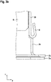
- Figure 3a shows a perspective, sectional view of a first connecting means 6 attached to an electrode plate (here, for example, the third electrode plate 3a) and a second connecting means 9a extending from a busbar (here, for example, the first busbar 7a) in a first position before connection.
- the first connecting means 6 is formed here in the manner of a bent tab, which is produced in one piece with the first electrode plate 2a.
- the second connecting means 9a consists of two tongues which extend from the first busbar 7a and converge at a free end of the first connecting means 6 .
- the first connecting means 6 can be inserted with a friction fit into the second connecting means 9a, which is designed as a tab.
- 3c shows the intermediate circuit capacitor module 1, which is connected to the power electronics module 8 by means of the plug connection in a second position, the second connecting means 9a having been deformed to produce the non-detachable connection.
- FIG. 4 shows a perspective partial view of a power electronics device 14, which includes the intermediate circuit capacitor module 1 connected to the power electronics module 8 and a cover element 15, in an assembled state.
- the power electronics module 8 includes other power electronics components, not shown, which implement a function as a charging device for an energy store, as an inverter or as a DC voltage converter.
- the cover element 15 rests on the second busbar 7b and is sealed off from it by means of a seal 16 .
- the cover element 15 is designed to be deformable, so that pressure equalization is possible without gas exchange between the interior 17 of the cover element, which accommodates the rolls 4, 5, and the environment.
Landscapes
- Engineering & Computer Science (AREA)
- Power Engineering (AREA)
- Microelectronics & Electronic Packaging (AREA)
- Manufacturing & Machinery (AREA)
- Inverter Devices (AREA)
- Dc-Dc Converters (AREA)
- Power Conversion In General (AREA)
Description
- Die Erfindung betrifft eine Leistungselektronikeinrichtung, insbesondere zur Verwendung in Elektrofahrzeugen.
- Nach dem Stand der Technik sind Leistungselektronikeinrichtungen, beispielsweise Ladeeinrichtungen für Energiespeicher, Inverter oder Gleichspannungswandler allgemein bekannt. Eine solche Leistungselektronikeinrichtung umfasst einen Gleichspannungszwischenkreis mit einem Zwischenkreiskondensator.
- Bei Leistungselektronikeinrichtungen mit Gleichspannungszwischenkreis, welche beispielsweise für Anwendungen in Fahrzeugen mit kombiniertem oder ausschließlichem elektrischen Antrieb vorgesehen sind, kommen häufig sehr leistungsfähige Leistungshalbleiter oder Leistungshalbleitermodule zum Einsatz. Diese sind in der Lage, mittels teilweise komplexer Regelungsverfahren und geeigneter Ansteuerverfahren, große elektrische Leistungen mittels hoher Schaltgeschwindigkeiten bedarfsgerecht zu schalten. Das schnelle Schalten von hohen Strömen am Gleichspannungszwischenkreis führt in Kombination mit aufbaubedingten Induktivitäten, insbesondere Leitungsinduktivitäten, während eines Ausschaltvorgangs des Leistungshalbleiter bzw. Leistungshalbleitermodule jedoch oft zu unerwünschten Spannungsspitzen. Meist verursachen hochfrequente Schaltvorgänge der Leistungshalbleiter bzw. Leistungshalbleitermodule am Gleichspannungszwischenkreis aus noch Beeinträchtigungen der elektromagnetischen Verträglichkeit.
- Es ist bekannt, diesen unerwünschten elektrischen Effekten mit dem Einsatz des Zwischenkreiskondensators im Gleichspannungszwischenkreis entgegenzuwirken. Entscheidend für den Erfolg dieser Maßnahme ist es insbesondere, dass mittels entsprechender Aufbau- und Verbindungstechnologien eine möglichst gute elektrische und mechanische Anbindung des Zwischenkreiskondensators an den Leistungshalbleiter bzw. die Leistungshalbleitermodule hergestellt wird.
- Ein Zwischenkreiskondensator ist üblicherweise aus zwei einander gegenüberliegenden Elektrodenplatten gebildet, zwischen denen ein oder mehrere Wickel gehalten sind. Jeder Wickel weist zwei einander gegenüberliegende Stirnseiten auf, die durch Schoopierung elektrisch kontaktierbar sind. Die schoopierten Stirnflächen werden üblicherweise an die jeweilige Elektrodenplatte angelötet oder angeschweißt. Die Elektrodenplatte ihrerseits ist wiederum fest mit einer Stromschiene verbunden, welche ein Anschlusselement zur Verbindung mit einer externen Schaltung, Leitung oder dgl. aufweist. Bei bestimmten Ausführungsformen sind die Elektrodenplatte mit den dazwischen gehaltenen Wickeln sowie die Stromschienen mit Ausnahme der darin vorgesehenen Anschlusselemente mit einer Vergussmasse vergossen. Zwischenkreiskondensatoren werden von den Herstellern von Leistungselektronikeinrichtungen üblicherweise von Lieferanten zugekauft, welche die Zwischenkreiskondensatoren nach Vorgaben der Hersteller fertigen. Bei einer Änderung der Vorgabe eines Herstellers ist es also erforderlich, dass der Lieferant gesondert einen entsprechend angepassten Zwischenkreiskondensator fertigt. Das ist umständlich und aufwändig.
- Die
DE 10 2008 050452 A1 offenbart eine Kondensatoranordnung, mit einem Kondensator mit einer ersten Kontaktfläche und einer zweiten Kontaktfläche, wobei die erste und die zweite Kontaktfläche gegenüberliegend angeordnet sind; einem ersten Anschlussblech, das mit der ersten Kontaktfläche verbunden ist, wobei das erste Anschlussblech an einem Ende Fortsätze aufweist, die geeignet sind, um in Ausnehmungen eines ersten abgewinkelten Bereichs einer ersten Leistungsschiene eines Leistungselektronikmoduls einzugreifen; und einem zweiten Anschlussblech, das mit der zweiten Kontaktfläche verbunden ist, wobei das zweite Anschlussblech an einem Ende Fortsätze aufweist, die geeignet sind, um in Ausnehmungen eines ersten abgewinkelten Bereichs einer zweiten Leistungsschiene des Leistungselektronikmoduls einzugreifen, so dass der Kondensator direkt in dem Leistungselektronikmodul angeordnet sein kann. Die Anschlussbleche sind mit den Leistungsschienen durch eine Steckverbindung mittels der Fortsätze und den Ausnehmungen verbunden. - Die
US 2011/102966 A1 offenbart einen vergossenen Kondensator mit einer Kondensatorelementanordnung, die ein erstes Kondensatorelement, ein zweites Kondensatorelement und eine Stromschiene, welche einen Anschluss aufweist und mit einer ersten Elektrode des ersten Kondensatorelements verfügt ist, umfasst. Das zweite Kondensatorelement ist mit der Stromschiene verfügt und mit dem ersten Kondensatorelement verbunden. - Aufgabe der Erfindung ist es, die Nachteile nach dem Stand der Technik zu beseitigen. Es soll insbesondere eine Leistungselektronikeinrichtung angegeben werden, welcher mit vermindertem Aufwand herstellbar ist.
- Diese Aufgabe wird durch die Merkmale des Patentanspruchs 1 gelöst. Zweckmäßige Ausgestaltungen der Erfindung ergeben sich aus den Merkmalen der abhängigen Patentansprüche.
- Bei dem Zwischenkreiskondensatormodul ist an zwei einander gegenüberliegenden Elektrodenplatten ein Wickel elektrisch leitend angebracht, wobei an jeder Elektrodenplatte mehrere erste Verbindungsmittel zur Herstellung einer Steckverbindung mit dazu korrespondierenden, an einer Stromschiene eines Leistungselektronikmoduls angebrachten zweiten Verbindungsmitteln vorgesehen sind.
- Das Zwischenkreiskondensatormodul weist in Abweichung vom Stand der Technik keine Stromschienen auf. Es sind lediglich an jeder Elektrodenplatte erste Verbindungsmittel vorgesehen, welche zur Verbindung mit an den Stromschienen vorgesehenen zweiten Verbindungsmitteln geeignet sind. Damit ist es möglich, die Stromschienen mit den daran vorgesehen zweiten Verbindungsmitteln im Leistungselektronikmodul zu montieren und sodann in einem späteren Fertigungsschritt das Zwischenkreiskondensatormodul mittels einer einfachen Steckverbindung elektrisch leitend mit den Stromschienen zu verbinden.
- Das Zwischenkreiskondensatormodul kann weitere an den Elektrodenplatten elektrisch leitend angebrachte Wickel aufweisen. Das Zwischenkreiskondensatormodul kann lieferantenseitig je nach Anforderung des Herstellers von Leistungselektronikeinrichtungen mit einer unterschiedlichen Anzahl an Wickeln und/oder Wickeln unterschiedlicher Eigenschaften versehen sein. Unabhängig davon können die Geometrie der Elektrodenplatten sowie die Anordnung und Ausbildung der ersten Verbindungsmittel beibehalten werden. Damit ist es herstellerseitig möglich, unter Beibehaltung der Montagegeometrie der am Leistungselektronikmodul angebrachten Stromschienen schnell und einfach Zwischenkreiskondensatormodule zu montieren, welche beispielsweise eine unterschiedliche Kapazität aufweisen. Seitens des Lieferanten entfällt der kosten- und zeitaufwändige Schritt der Montage der Stromschiene an die Elektrodenplatten. Abgesehen davon können derartige Zwischenkreiskondensatormodule auch in kleineren Einheiten lieferantenseitig vorgehalten werden, von denen dann auch mehrere herstellerseitig mittels der Steckverbindung auf die Stromschienen montiert werden können.
- Nach einer besonders vorteilhaften Ausgestaltung ist das erste Verbindungsmittel einstückig mit der Elektrodenplatte ausgebildet. Das erste Verbindungsmittel kann beispielsweise mittels Stanz-, Laserschneid- und Biegetechnik in einem Stück mit der Elektrodenplatte hergestellt sein. Das erste Verbindungsmittel kann insbesondere nach Art einer zur Aufnahme eines Kontaktstifts geeigneten Buchse oder Lasche ausgebildet sein. Die Buchse oder Lasche kann beispielsweise eine Klemmfeder oder dgl. aufweisen.
- Nach einer weiteren vorteilhaften Ausgestaltung sind in paralleler Anordnung ein aus den Elektrodenplatten gebildetes erstes Elektrodenplattenpaar mit dem dazwischen aufgenommenen ersten Wickel und ein aus zwei weiteren einander gegenüberliegenden Elektrodenplatten gebildetes zweites Elektrodenplattenpaar mit einem oder mehreren dazwischen aufgenommenen zweiten Wickeln vorgesehen Die vorgeschlagene Untergliederung des Zwischenkreiskondensatormoduls in ein erstes und ein zweites Elektrodenplattenpaar mit jeweils dazwischen gehaltenen Wickeln ermöglicht bei Beibehaltung einer vorgegebenen Geometrie eine Verminderung der zwischen den Elektrodenplatten aufgespannten Flächen. Infolgedessen wird eine Streu-Induktivität des Zwischenkreiskondensatormoduls herabgesetzt. Ein solches Zwischenkreiskondensatormodul eignet sich für besonders schnelle Schaltvorgänge.
- Bei dem Leistungselektronikmodul mit zumindest zwei Stromschienen sind an jeder Stromschiene zweite Verbindungsmittel zur Herstellung der Steckverbindung mit den dazu korrespondierenden, an dem Zwischenkreiskondensatormodul angebrachten ersten Verbindungsmitteln vorgesehen.
- Das Leistungselektronikmodul kann herstellerseitig vorteilhafterweise zunächst ohne das Zwischenkreiskondensatormodul hergestellt werden. Es kann in einem späteren Fertigungsschritt schnell und einfach durch Herstellung einer Steckverbindung mit dem Zwischenkreiskondensatormodul verbunden werden. Infolgedessen ist es beispielsweise möglich, die Stromschienen herstellerseitig so zu montieren, dass sie nahe an einer Kühleinrichtung angebracht oder unmittelbar in Kontakt mit einer Kühleinrichtung sind. Die Stromschienen können jeweils mit einer standardisierten Anordnung an zweiten Verbindungsmitteln versehen sein. Damit ist es möglich, einen oder mehrere geometrisch entsprechend angepasste Zwischenkreiskondensatormodule an den Stromschienen zu montieren.
- Die Stromschienen können in einander gegenüberliegender Anordnung, insbesondere sandwichartig, montiert sein. Eine Stromschiene kann Durchbrechungen zum Durchführen der zweiten Verbindungsmittel der anderen Stromschiene aufweisen.
- Nach einer vorteilhaften Ausgestaltung ist das zweite Verbindungsmittel nach Art eines sich von der Stromschiene erstreckenden Kontaktstifts ausgebildet, welcher reibschlüssig in das erste Verbindungsmittel einsteckbar ist. Der Begriff "Kontaktstift" ist vorliegend allgemein zu verstehen, d. h. es kann sich dabei auch um eine oder mehrere nebeneinander angeordnete Kontaktzungen handeln, welche beispielsweise in Draufsicht rechteckig, trapezförmig oder spitzzulaufend ausgebildet sind. Der Kontaktstift kann auch als Stift oder Rohrstutzen ausgebildet sein. Er kann im Querschnitt rund, quadratisch oder rechteckig sein.
- Das zweite Verbindungsmittel ist zweckmäßigerweise einstückig mit der Stromschiene ausgebildet. Das zweite Verbindungsmittel kann beispielsweise mittels Stanzen, Laserschneiden und Umbiegen ausgebildet sein.
- Die Stromschiene kann ein Anschlusselement zum Anschluss an eine Versorgungsleitung, eine Schaltung oder dgl. aufweisen. Es handelt sich dabei beispielsweise um eine Anschlussfahne mit einem Durchbruch zum Durchführen eines Befestigungselements, beispielsweise einer Schraube, eines Gewindebolzens oder dgl.
- Bevorzugt ist das Leistungselektronikmodul als Ladeeinrichtung für einen elektrischen Energiespeicher, als Inverter oder als Gleichspannungswandler ausgebildet.
- Bei der vorgeschlagenen Leistungselektronikeinrichtung ist das Zwischenkreiskondensatormodul mittels der Steckverbindung mit den Stromschienen des Leistungselektronikmoduls Eine solche Leistungselektronikeinrichtung lässt sich mit verringertem Aufwand herstellen. Er lässt sich - je nach Anforderung - auch mit mehreren Zwischenkreiskondensatormodulen gleicher oder unterschiedlicher Kapazität, Spannungsfestigkeit, Streuinduktivität und dgl. kombinieren. Ferner kann mit der vorgeschlagenen Trennung der Stromschienen vom Zwischenkreiskondensatormodul eine verbesserte Kühlung des Zwischenkreiskondensatormoduls erreicht werden. Die Stromschienen können herstellerseitig so im Leistungselektronikmodul angebracht werden, dass sie mit verbesserter Effizienz gekühlt werden können.
- Die erfindungsgemäße Leistungselektronikeinrichtung kann ferner ein Deckelelement, welches die Wickel gasdicht einhaust umfassen. Das Deckelelement schützt die Wickel vor Feuchtigkeit und Wärme, die insbesondere beim Transport die Wickel schädigen kann. Besonders bevorzugt ist das Deckelelement verformbar, um einen Druckausgleich ohne Gasaustausch zwischen den im Inneren des Deckelelements aufgenommenen Wickeln und der Umgebung zu ermöglichen. Insbesondere kann so auf üblicherweise verwendete metallisierte Einwegfolien, in die herkömmliche Wickel beim Transport eingeschweißt werden, verzichtet werden.
- Daneben kann die Leistungselektronikeinrichtung ein das Deckelelement gegenüber einer Stromschiene abdichtendes Dichtelement umfassen. Das Deckelelement kann dabei auf der Stromschiene aufliegen.
- Nach dem Herstellen der Steckverbindung wird das zweite Verbindungsmittel verformt, so dass die Verbindung unlösbar wird, d. h. ohne eine Verformung oder Zerstörung der Verbindungsmittel nicht mehr lösbar ist.
- Nachfolgend werden vorteilhafte Ausgestaltungen der Erfindung anhand der Zeichnungen näher erläutert. Es zeigen:
- Fig. 1
- eine perspektivische Teilansicht einer ersten Leistungselektronikeinrichtung,
- Fig. 2
- eine perspektivische Teilansicht einer zweiten Leistungselektronikeinrichtung,
- Fig. 3a
- eine perspektivische geschnittene Ansicht erster und zweiter Verbindungsmittel in einer ersten Position,
- Fig. 3b
- eine geschnittene Seitenansicht der ersten und zweiten Verbindungsmittel in der ersten Position,
- Fig. 3c
- eine geschnittene perspektivische Ansicht der ersten und zweiten Verbindungsmittel in einer zweiten Position und
- Fig. 4
- eine perspektivische Ansicht einer Leistungselektronikeinrichtung in einem montierten Zustand.
-
Fig. 1 zeigt ein allgemein mit dem Bezugszeichen 1 bezeichnetes Zwischenkreiskondensatormodul. Das Zwischenkreiskondensatormodul 1 weist eine erste Elektrodenplatte 2a und eine zweite Elektrodenplatte 2b, welche einander gegenüber liegen und ein erstes Elektrodenplattenpaar 2 bilden, sowie eine dritte Elektrodenplatte 3a und eine vierte Elektrodenplatte 3b auf, welche ebenfalls einander gegenüber liegen und ein zweites Elektrodenplattenpaar 3 bilden. Zwischen dem ersten Elektrodenplattenpaar 2 sind mehrere erste Wickel 4 und zwischen dem zweiten Elektrodenplattenpaar 3 zweite Wickel 5 angebracht. Die Wickel 4, 5 sind stirnseitig schoopiert. Mittels Löten, Schweißen oder einer anderen Verbindungstechnik sind die Wickel 4 mit den Elektrodenplatten 2a, 2b und die Wickel 5 mit den Elektrodenplatten 3a, 3b verbunden. - Die Elektrodenplatten 2a, 2b, 3a, 3b sind jeweils mit ersten Verbindungsmitteln 6 versehen. Bei den ersten Verbindungsmitteln 6 handelt es sich hier um einstückig mit den Elektrodenplatten 2a, 2b, 3a, 3b ausgebildete, umgebogene Laschen.
-
Fig. 1 zeigt ferner eine erste Stromschiene 7a und eine (hier teilweise verdeckte) zweite Stromschiene 7b eines Leistungselektronikmoduls 8. Die Stromschienen 7a, 7b sind sandwichartig voneinander elektrisch isoliert angeordnet. Von den Stromschienen 7a, 7b erstrecken sich zweite Verbindungsmittel 9a, 9b, welche nach Art einer Stecklasche ausgebildet sind. Die sich von der ersten Stromschiene 7a erstreckenden zweiten Verbindungsmittel 9a durchsetzen Durchbrüche 10 der zweiten Stromschiene 7b. - Die ersten Verbindungsmittel 6 und die zweiten Verbindungsmittel 9a, 9b sind korrespondierend zur Herstellung einer unlösbaren Steckverbindung ausgebildet. Eine Anordnung der ersten Verbindungsmittel 6 am Zwischenkreiskondensatormodul 1 ist korrespondierend zur Anordnung der zweiten Verbindungsmittel 9a, 9b an den Stromschienen 7a, 7b so dass zwischen sämtlichen ersten Verbindungsmitteln 6 und sämtlichen zweiten Verbindungsmitteln 9 beim Aufsetzen des Zwischenkreiskondensatormoduls 1 auf die Stromschienen 7a, 7b die Steckverbindung herstellbar ist.
- Die erste Stromschiene 7a ist mit einem ersten Anschlusselement 11a verbunden. Die zweite Stromschiene 7b ist mit einem zweiten Anschlusselement 11b verbunden. Die Anschlusselemente 11a und 11b weisen jeweils einen Durchbruch 12 auf, durch welche beispielsweise Schrauben zur Verbindung mit Stromleitungen geführt werden können.
- Die in
Fig. 1 gezeigte Anordnung der Stromschienen 7a, 7b ist fester Bestandteil des Leistungselektronikmoduls 8. Das Zwischenkreiskondensatormodul 1 wird mittels der Steckverbindung mit dem Leistungselektronikmodul 8 zu einer Leistungselektronikeinrichtung 14 verbunden. - Wie insbesondere aus
Fig. 2 ersichtlich ist, können bei gleichbleibender Ausbildung der Stromschienen 7a, 7b auch ein weiteres andersartig ausgestaltetes Zwischenkreiskondensatormodul 1', mit der ersten Stromschiene 7a und zweiten Stromschiene 7b, verbunden werden. Das weitere Zwischenkreiskondensatormodul 1' weist lediglich eine erste Elektrodenplatte 2a und eine zweite Elektrodenplatten 2b auf, die ein Elektrodenplattenpaar 2 bilden und zwischen denen mehrere erste Wickel 4 gehalten sind. Indem hinsichtlich der Anordnung und Ausbildung der Stromschienen 7a, 7b und der daran vorgesehenen zweiten Verbindungsmittel 9a, 9b das Leistungselektronikmodul 8 standardisiert ist, können damit hinsichtlich der Anordnung und Ausbildung der ersten Verbindungsmittel korrespondierend ausgebildete Zwischenkreiskondensatormodule 1, 1' ohne großen Aufwand mittels der Steckverbindung verbunden werden. Die Zwischenkreiskondensatormodule 1, 1' können allerdings hinsichtlich der Anzahl und Ausgestaltung der Elektrodenplatten 2a, 2b, 3a, 3b und der dazwischen gehaltenen Wickel 4, 5 unterschiedlich ausgestaltet sein. Damit ist es möglich, Zwischenkreiskondensatormodule 1, 1' unterschiedlicher Kapazität, Streuinduktivität oder dgl. mit dem Leistungselektronikmodul 8 zu kombinieren. -
Fig. 3a zeigt eine perspektivische, geschnittene Ansicht eines an einer Elektrodenplatte (hier beispielhaft der dritten Elektrodenplatte 3a) angebrachten ersten Verbindungsmittels 6 sowie ein sich von einer Stromschiene (hier beispielhaft der ersten Stromschiene 7a) erstreckendes zweites Verbindungsmittel 9a in einer ersten Position vor einem Verbinden. Wie insbesondere in Zusammensicht mit einer inFig. 3b gezeigten geschnittenen Seitenansicht ersichtlich ist, ist das erste Verbindungsmittel 6 hier nach Art einer umgebogenen Lasche gebildet, welche in einstückiger Ausbildung mit der ersten Elektrodenplatte 2a hergestellt ist. Das zweite Verbindungsmittel 9a besteht aus zwei sich von der ersten Stromschiene 7a erstreckenden Zungen, welche an einem freien Ende des ersten Verbindungsmittels 6 zusammenlaufen. Das erste Verbindungsmittel 6 ist in das als Lasche ausgebildete zweite Verbindungsmittel 9a reibschlüssig einsteckbar.Fig. 3c zeigt das Zwischenkreiskondensatormodul 1, welches mittels der Steckverbindung mit dem Leistungselektronikmodul 8 in einer zweiten Position verbunden ist, wobei das zweite Verbindungsmittel 9a zur Herstellung der unlösbaren Verbindung verformt worden ist. -
Fig. 4 zeigt eine perspektivische Teilansicht einer Leistungselektronikeinrichtung 14, welche das mit dem Leistungselektronikmodul 8 verbundene Zwischenkreiskondensatormodul 1 sowie ein Deckelelement 15 umfasst, in einem montierten Zustand. Daneben umfasst das Leistungselektronikmodul 8 weitere nicht gezeigte Leistungselektronikkomponenten, welche eine Funktion als Ladeeinrichtung für einen Energiespeicher, als Inverter oder als Gleichspannungswandler realisieren. - Das Deckelelement 15 liegt auf der zweiten Stromschiene 7b auf und ist mittels einer Dichtung 16 dieser gegenüber abgedichtet. Das Deckelelement 15 ist verformbar ausgebildet, so dass ein Druckausgleich ohne Gasaustausch zwischen dem die Wickel 4, 5 aufnehmenden Inneren 17 des Deckelelements und der Umgebung möglich ist.
Claims (11)
- Leistungselektronikeinrichtung (14), umfassend:ein Zwischenkreiskondensatormodul (1, 1'), bei dem an zwei einander gegenüberliegenden Elektrodenplatten (2a, 2b) ein Wickel (4, 5) elektrisch leitend angebracht ist; undein Leistungselektronikmodul (8) mit zumindest zwei Stromschienen (7a, 7b); wobei das Zwischenkreiskondensatormodul (1, 1') mittels einer Steckverbindung mit dem Leistungselektronikmodul (8) verbunden ist;wobei an jeder Elektrodenplatte (2a, 2b) mehrere erste Verbindungsmittel (6) zur Herstellung der Steckverbindung mit dazu korrespondierenden, an den Stromschienen (7a, 7b) des Leistungselektronikmoduls (8) angebrachten, zweiten Verbindungsmitteln (9a, 9b) vorgesehen sind;wobei an jeder Stromschiene (7a, 7b) die zweiten Verbindungsmittel (9a, 9b) zur Herstellung der Steckverbindung mit den dazu korrespondierenden, an den Elektrodenplatten (2a, 2b) des Zwischenkreiskondensatormoduls (1, 1') angebrachten, ersten Verbindungsmitteln (6) vorgesehen sind,dadurch gekennzeichnet, dassnach dem Herstellen der Steckverbindung die zweiten Verbindungsmittel (9a, 9b) verformt worden sind, so dass die Steckverbindung ohne eine Verformung oder Zerstörung der Verbindungsmittel (6, 9a, 9b) nicht mehr lösbar ist.
- Leistungselektronikeinrichtung (14) nach Anspruch 1, wobei die ersten Verbindungsmittel (6) einstückig mit der Elektrodenplatte (2a, 2b, 3a, 3b) ausgebildet sind.
- Leistungselektronikeinrichtung (14) nach Anspruch 1 oder 2, wobei die ersten Verbindungsmittel (6) nach Art einer zur Aufnahme eines Kontaktstifts geeigneten Buchse oder Lasche ausgebildet sind.
- Leistungselektronikeinrichtung (14) nach einem der vorhergehenden Ansprüche, wobei in paralleler Anordnung ein aus den Elektrodenplatten (2a, 2b) gebildetes erstes Elektrodenplattenpaar (2) mit dem dazwischen aufgenommenen ersten Wickel (4) und ein aus zwei weiteren einander gegenüberliegenden Elektrodenplatten (3a, 3b) gebildetes zweites Elektrodenplattenpaar (3) mit einem dazwischen aufgenommenen zweiten Wickel (5) vorgesehen sind.
- Leistungselektronikeinrichtung (14) nach Anspruch 4, wobei eine erste Elektrodenplatte (2a) des ersten Elektrodenplattenpaars (2) mit einer dritten Elektrodenplatte (3a) des zweiten Elektrodenplattenpaars (3), und eine zweite Elektrodenplatte (2b) des ersten Elektrodenplattenpaars (2) mit einer vierten Elektrodenplatte (3b) des zweiten Elektrodenplattenpaars (3) verbunden ist.
- Leistungselektronikeinrichtung (14) nach einem der vorhergehenden Ansprüche, wobei die zweiten Verbindungsmittel (9a, 9b) einstückig mit der Stromschiene (7a, 7b) ausgebildet sind.
- Leistungselektronikeinrichtung (14) nach einem der vorhergehenden Ansprüche, wobei die zweiten Verbindungsmittel (9a, 9b) nach Art eines sich von der Stromschiene (7a, 7b) erstreckenden Kontaktstifts ausgebildet sind, welche reibschlüssig in die ersten Verbindungsmittel (6) einsteckbar sind.
- Leistungselektronikeinrichtung (14) nach einem der vorhergehenden Ansprüche, wobei eine der Stromschienen (7a, 7b) ein Anschlusselement (11a, 11b) zum Anschluss an eine Versorgungsleitung aufweist.
- Leistungselektronikeinrichtung (14) nach einem der vorhergehenden Ansprüche, wobei die Leistungselektronikeinrichtung (14) als Ladeeinrichtung für einen elektrischen Energiespeicher, als Inverter oder als Gleichspannungswandler ausgebildet ist.
- Leistungselektronikeinrichtung (14) nach einem der vorhergehenden Ansprüche, ferner umfassend ein, insbesondere verformbares, Deckelelement (15), welches die Wickel (4, 5) gasdicht einhaust.
- Leistungselektronikeinrichtung (14) nach Anspruch 10, ferner umfassend ein das Deckelelement (15) gegenüber einer Stromschiene (7a, 7b) abdichtendes Dichtelement (16).
Applications Claiming Priority (2)
| Application Number | Priority Date | Filing Date | Title |
|---|---|---|---|
| DE102017126394.2A DE102017126394A1 (de) | 2017-11-10 | 2017-11-10 | Zwischenkreiskondensatormodul, Leistungselektronikmodul und Leistungselektronikeinrichtung |
| PCT/EP2018/080564 WO2019092077A1 (de) | 2017-11-10 | 2018-11-08 | Zwischenkreiskondensatormodul, leistungselektronikmodul und leistungselektronikeinrichtung |
Publications (2)
| Publication Number | Publication Date |
|---|---|
| EP3707737A1 EP3707737A1 (de) | 2020-09-16 |
| EP3707737B1 true EP3707737B1 (de) | 2022-08-17 |
Family
ID=64308729
Family Applications (1)
| Application Number | Title | Priority Date | Filing Date |
|---|---|---|---|
| EP18803368.2A Active EP3707737B1 (de) | 2017-11-10 | 2018-11-08 | Leistungselektronikeinrichtung |
Country Status (6)
| Country | Link |
|---|---|
| US (1) | US11417470B2 (de) |
| EP (1) | EP3707737B1 (de) |
| JP (1) | JP2021502702A (de) |
| CN (1) | CN111344823B (de) |
| DE (1) | DE102017126394A1 (de) |
| WO (1) | WO2019092077A1 (de) |
Families Citing this family (11)
| Publication number | Priority date | Publication date | Assignee | Title |
|---|---|---|---|---|
| DE102021113683A1 (de) | 2021-05-27 | 2022-12-01 | Schaeffler Technologies AG & Co. KG | Kondensatormodul für eine Wechselrichterelektronik |
| EP4125104A1 (de) | 2021-07-15 | 2023-02-01 | Valeo eAutomotive France SAS | Stromwandler |
| EP4125103A1 (de) | 2021-07-15 | 2023-02-01 | Valeo eAutomotive France SAS | Kondensatorzelle |
| DE102021209859A1 (de) * | 2021-09-07 | 2023-03-09 | Valeo Eautomotive Germany Gmbh | Zwischenkreiskondensator für einen Stromrichter, insbesondere für einen Wechselrichter |
| DE102021209858A1 (de) | 2021-09-07 | 2023-03-09 | Valeo Eautomotive Germany Gmbh | Filmkondensatorelement, insbesondere für einen Zwischenkreiskondensator in einem Stromrichter |
| EP4184536A1 (de) | 2021-11-23 | 2023-05-24 | Valeo eAutomotive France SAS | Gehäuse mit fächern für gleichspannungskondensatoren und abdichtung |
| CN114391949B (zh) * | 2021-12-15 | 2024-04-16 | 深圳爱博合创医疗机器人有限公司 | 一种多路走线介入手术机器人 |
| DE102022207478A1 (de) * | 2022-07-21 | 2024-02-01 | Zf Friedrichshafen Ag | Modularer Zwischenkreiskondensator und Stromrichter mit einem derartigen Zwischenkreiskondensator |
| FR3158583B1 (fr) * | 2024-01-24 | 2025-12-26 | Valeo Eautomotive Germany Gmbh | Condensateur pour bus continu d’un onduleur |
| WO2025237539A1 (de) * | 2024-05-17 | 2025-11-20 | Pierburg Gmbh | Kondensator-modul |
| US20250385043A1 (en) * | 2024-06-12 | 2025-12-18 | BorgWarner US Technologies LLC | Systems for capacitor for inverter for electric vehicle |
Citations (1)
| Publication number | Priority date | Publication date | Assignee | Title |
|---|---|---|---|---|
| DE102008050452B4 (de) * | 2008-10-08 | 2010-09-16 | Mtu Aero Engines Gmbh | Kontaktierungsanordnung für einen Kondensator, Leistungsmodul und Verfahren zum Herstellen eines Leistungsmoduls |
Family Cites Families (15)
| Publication number | Priority date | Publication date | Assignee | Title |
|---|---|---|---|---|
| US3806766A (en) * | 1972-12-27 | 1974-04-23 | Western Electric Co | Packaged electrical component assembly and method of fabrication |
| JPH0291331U (de) * | 1988-12-29 | 1990-07-19 | ||
| JP4747560B2 (ja) * | 2004-11-17 | 2011-08-17 | パナソニック株式会社 | フィルムコンデンサおよびその製造方法 |
| JP2009136041A (ja) * | 2007-11-28 | 2009-06-18 | Autonetworks Technologies Ltd | 回路保護材および回路保護材の接続構造 |
| CN102089839B (zh) | 2008-07-10 | 2013-04-03 | 松下电器产业株式会社 | 模制电容器和其制造方法 |
| JP5424030B2 (ja) * | 2009-08-31 | 2014-02-26 | 株式会社指月電機製作所 | コンデンサ |
| US20110228442A1 (en) * | 2010-03-16 | 2011-09-22 | Strategic Polymer Sciences, Inc. | Capacitor having high temperature stability, high dielectric constant, low dielectric loss, and low leakage current |
| DE102011007307A1 (de) * | 2011-04-13 | 2012-10-18 | Robert Bosch Gmbh | Speichereinheit zum Speichern elektrischer Energie mit einem Kühlelement |
| US8787003B2 (en) * | 2011-10-12 | 2014-07-22 | Infineon Technologies Ag | Low inductance capacitor module and power system with low inductance capacitor module |
| KR101506231B1 (ko) * | 2013-06-25 | 2015-03-26 | 삼화콘덴서공업주식회사 | 차량용 전력전자 커패시터 모듈 |
| JP6400673B2 (ja) * | 2014-03-03 | 2018-10-03 | 京セラ株式会社 | フィルムコンデンサおよび連結型コンデンサ、ならびにインバータ、電動車輌 |
| CN105529188A (zh) * | 2014-11-28 | 2016-04-27 | 比亚迪股份有限公司 | 薄膜电容器 |
| CN105680266B (zh) * | 2016-04-11 | 2017-11-03 | 珠海英搏尔电气股份有限公司 | 交流电机控制器、叠层母排组件及其制作方法 |
| CN105845440B (zh) * | 2016-04-11 | 2017-09-01 | 珠海英搏尔电气股份有限公司 | 交流电机控制器、电容阵列及其制作方法 |
| CN206179679U (zh) * | 2016-11-28 | 2017-05-17 | 威斯康电容器有限公司 | 电容器安装底座 |
-
2017
- 2017-11-10 DE DE102017126394.2A patent/DE102017126394A1/de active Pending
-
2018
- 2018-11-08 JP JP2020525850A patent/JP2021502702A/ja not_active Ceased
- 2018-11-08 US US16/762,327 patent/US11417470B2/en active Active
- 2018-11-08 EP EP18803368.2A patent/EP3707737B1/de active Active
- 2018-11-08 WO PCT/EP2018/080564 patent/WO2019092077A1/de not_active Ceased
- 2018-11-08 CN CN201880072625.5A patent/CN111344823B/zh active Active
Patent Citations (1)
| Publication number | Priority date | Publication date | Assignee | Title |
|---|---|---|---|---|
| DE102008050452B4 (de) * | 2008-10-08 | 2010-09-16 | Mtu Aero Engines Gmbh | Kontaktierungsanordnung für einen Kondensator, Leistungsmodul und Verfahren zum Herstellen eines Leistungsmoduls |
Also Published As
| Publication number | Publication date |
|---|---|
| WO2019092077A1 (de) | 2019-05-16 |
| EP3707737A1 (de) | 2020-09-16 |
| US11417470B2 (en) | 2022-08-16 |
| DE102017126394A1 (de) | 2019-05-16 |
| CN111344823A (zh) | 2020-06-26 |
| CN111344823B (zh) | 2022-10-21 |
| US20210110978A1 (en) | 2021-04-15 |
| JP2021502702A (ja) | 2021-01-28 |
Similar Documents
| Publication | Publication Date | Title |
|---|---|---|
| WO2019092077A1 (de) | Zwischenkreiskondensatormodul, leistungselektronikmodul und leistungselektronikeinrichtung | |
| EP2328392B1 (de) | Umrichter, insbesondere mehrphasiger Drehstromumrichter | |
| EP3363105B1 (de) | Platine, b-lagerschild, motorbausatz und elektromotor | |
| EP3349344B1 (de) | Filteranordnung | |
| EP2328391B1 (de) | Umrichter | |
| DE102017109706B3 (de) | Leistungselektronische Anordnung mit Gleichspannungsverbindungselement | |
| EP3358921B1 (de) | Leistungselektronische anordnung und fahrzeug hiermit | |
| DE102020211091A1 (de) | Elektrischer Kontaktverbinder sowie Batterie | |
| EP2608323A1 (de) | Gehäusedurchführungsverbinder | |
| DE102012104259B4 (de) | Gleichstrommotor zum Antrieb von Aggregaten eines Kraftfahrzeugs | |
| EP2328390A2 (de) | Umrichter mit einem Kühlkörper | |
| DE102012018086A1 (de) | Stromschienenanordnung | |
| WO2018108498A1 (de) | Entkopplungselement zur verbindung einer leistungselektronik mit einer elektrischen maschine | |
| DE112019000450T5 (de) | Elektrischer Kompressor | |
| DE102019133954B4 (de) | Anordnung zur Filterung von Störungen | |
| WO2023052298A1 (de) | Elektrische verschaltungseinrichtung für einen stator und verfahren zum herstellen einer elektrischen verschaltungseinrichtung für einen stator | |
| DE102017206146B4 (de) | Hochstrom-Steckbuchse und Hochstrom-Steckeranordnung mit einer Hochstrom-Steckbuchse | |
| EP3329753A1 (de) | Elektrische schaltungsanordnung mit kondensator mit gehäusefunktion | |
| DE112016000036T5 (de) | Anschlussverbindungsstruktur eines Leistungshalbleitermoduls | |
| EP3408857B1 (de) | Niederinduktiver elektrischer aussenanschluss für in einem gehäuse angeordnete wickel elektrischer leistungskondensatoren | |
| DE102012222704A1 (de) | Elektrischer Kondensator | |
| DE102012201752A1 (de) | Kondensator und Verfahren zum Herstellen eines Kondensators | |
| WO2013041078A1 (de) | Steckelement | |
| DE202010008274U1 (de) | Elektrische Verbindung zwischen zwei Busbars aus ebenen Leitern und einer zwischen den Leitern angeordneten Isolationsschicht | |
| DE102016208737A1 (de) | Montageadapter und Leistungsmodulsystem |
Legal Events
| Date | Code | Title | Description |
|---|---|---|---|
| STAA | Information on the status of an ep patent application or granted ep patent |
Free format text: STATUS: UNKNOWN |
|
| STAA | Information on the status of an ep patent application or granted ep patent |
Free format text: STATUS: THE INTERNATIONAL PUBLICATION HAS BEEN MADE |
|
| PUAI | Public reference made under article 153(3) epc to a published international application that has entered the european phase |
Free format text: ORIGINAL CODE: 0009012 |
|
| STAA | Information on the status of an ep patent application or granted ep patent |
Free format text: STATUS: REQUEST FOR EXAMINATION WAS MADE |
|
| 17P | Request for examination filed |
Effective date: 20200508 |
|
| AK | Designated contracting states |
Kind code of ref document: A1 Designated state(s): AL AT BE BG CH CY CZ DE DK EE ES FI FR GB GR HR HU IE IS IT LI LT LU LV MC MK MT NL NO PL PT RO RS SE SI SK SM TR |
|
| AX | Request for extension of the european patent |
Extension state: BA ME |
|
| DAV | Request for validation of the european patent (deleted) | ||
| DAX | Request for extension of the european patent (deleted) | ||
| STAA | Information on the status of an ep patent application or granted ep patent |
Free format text: STATUS: EXAMINATION IS IN PROGRESS |
|
| 17Q | First examination report despatched |
Effective date: 20210623 |
|
| GRAP | Despatch of communication of intention to grant a patent |
Free format text: ORIGINAL CODE: EPIDOSNIGR1 |
|
| STAA | Information on the status of an ep patent application or granted ep patent |
Free format text: STATUS: GRANT OF PATENT IS INTENDED |
|
| RIC1 | Information provided on ipc code assigned before grant |
Ipc: H02M 7/00 20060101ALN20220204BHEP Ipc: H01G 4/32 20060101ALN20220204BHEP Ipc: H01G 4/224 20060101ALN20220204BHEP Ipc: H01G 2/10 20060101ALN20220204BHEP Ipc: H01G 4/40 20060101ALI20220204BHEP Ipc: H01G 4/38 20060101ALI20220204BHEP Ipc: H01G 4/228 20060101ALI20220204BHEP Ipc: H01G 4/005 20060101ALI20220204BHEP Ipc: H01G 2/04 20060101AFI20220204BHEP |
|
| INTG | Intention to grant announced |
Effective date: 20220307 |
|
| GRAS | Grant fee paid |
Free format text: ORIGINAL CODE: EPIDOSNIGR3 |
|
| GRAA | (expected) grant |
Free format text: ORIGINAL CODE: 0009210 |
|
| STAA | Information on the status of an ep patent application or granted ep patent |
Free format text: STATUS: THE PATENT HAS BEEN GRANTED |
|
| REG | Reference to a national code |
Ref country code: DE Ref legal event code: R081 Ref document number: 502018010439 Country of ref document: DE Owner name: VALEO EAUTOMOTIVE GERMANY GMBH, DE Free format text: FORMER OWNER: VALEO SIEMENS EAUTOMOTIVE GERMANY GMBH, 91056 ERLANGEN, DE |
|
| AK | Designated contracting states |
Kind code of ref document: B1 Designated state(s): AL AT BE BG CH CY CZ DE DK EE ES FI FR GB GR HR HU IE IS IT LI LT LU LV MC MK MT NL NO PL PT RO RS SE SI SK SM TR |
|
| RAP4 | Party data changed (patent owner data changed or rights of a patent transferred) |
Owner name: VALEO EAUTOMOTIVE GERMANY GMBH |
|
| REG | Reference to a national code |
Ref country code: CH Ref legal event code: EP |
|
| REG | Reference to a national code |
Ref country code: DE Ref legal event code: R096 Ref document number: 502018010439 Country of ref document: DE |
|
| REG | Reference to a national code |
Ref country code: IE Ref legal event code: FG4D Free format text: LANGUAGE OF EP DOCUMENT: GERMAN |
|
| REG | Reference to a national code |
Ref country code: AT Ref legal event code: REF Ref document number: 1512709 Country of ref document: AT Kind code of ref document: T Effective date: 20220915 |
|
| REG | Reference to a national code |
Ref country code: NL Ref legal event code: MP Effective date: 20220817 |
|
| REG | Reference to a national code |
Ref country code: LT Ref legal event code: MG9D |
|
| PG25 | Lapsed in a contracting state [announced via postgrant information from national office to epo] |
Ref country code: SE Free format text: LAPSE BECAUSE OF FAILURE TO SUBMIT A TRANSLATION OF THE DESCRIPTION OR TO PAY THE FEE WITHIN THE PRESCRIBED TIME-LIMIT Effective date: 20220817 Ref country code: RS Free format text: LAPSE BECAUSE OF FAILURE TO SUBMIT A TRANSLATION OF THE DESCRIPTION OR TO PAY THE FEE WITHIN THE PRESCRIBED TIME-LIMIT Effective date: 20220817 Ref country code: PT Free format text: LAPSE BECAUSE OF FAILURE TO SUBMIT A TRANSLATION OF THE DESCRIPTION OR TO PAY THE FEE WITHIN THE PRESCRIBED TIME-LIMIT Effective date: 20221219 Ref country code: NO Free format text: LAPSE BECAUSE OF FAILURE TO SUBMIT A TRANSLATION OF THE DESCRIPTION OR TO PAY THE FEE WITHIN THE PRESCRIBED TIME-LIMIT Effective date: 20221117 Ref country code: NL Free format text: LAPSE BECAUSE OF FAILURE TO SUBMIT A TRANSLATION OF THE DESCRIPTION OR TO PAY THE FEE WITHIN THE PRESCRIBED TIME-LIMIT Effective date: 20220817 Ref country code: LV Free format text: LAPSE BECAUSE OF FAILURE TO SUBMIT A TRANSLATION OF THE DESCRIPTION OR TO PAY THE FEE WITHIN THE PRESCRIBED TIME-LIMIT Effective date: 20220817 Ref country code: LT Free format text: LAPSE BECAUSE OF FAILURE TO SUBMIT A TRANSLATION OF THE DESCRIPTION OR TO PAY THE FEE WITHIN THE PRESCRIBED TIME-LIMIT Effective date: 20220817 Ref country code: FI Free format text: LAPSE BECAUSE OF FAILURE TO SUBMIT A TRANSLATION OF THE DESCRIPTION OR TO PAY THE FEE WITHIN THE PRESCRIBED TIME-LIMIT Effective date: 20220817 |
|
| PG25 | Lapsed in a contracting state [announced via postgrant information from national office to epo] |
Ref country code: PL Free format text: LAPSE BECAUSE OF FAILURE TO SUBMIT A TRANSLATION OF THE DESCRIPTION OR TO PAY THE FEE WITHIN THE PRESCRIBED TIME-LIMIT Effective date: 20220817 Ref country code: IS Free format text: LAPSE BECAUSE OF FAILURE TO SUBMIT A TRANSLATION OF THE DESCRIPTION OR TO PAY THE FEE WITHIN THE PRESCRIBED TIME-LIMIT Effective date: 20221217 Ref country code: HR Free format text: LAPSE BECAUSE OF FAILURE TO SUBMIT A TRANSLATION OF THE DESCRIPTION OR TO PAY THE FEE WITHIN THE PRESCRIBED TIME-LIMIT Effective date: 20220817 Ref country code: GR Free format text: LAPSE BECAUSE OF FAILURE TO SUBMIT A TRANSLATION OF THE DESCRIPTION OR TO PAY THE FEE WITHIN THE PRESCRIBED TIME-LIMIT Effective date: 20221118 |
|
| PG25 | Lapsed in a contracting state [announced via postgrant information from national office to epo] |
Ref country code: SM Free format text: LAPSE BECAUSE OF FAILURE TO SUBMIT A TRANSLATION OF THE DESCRIPTION OR TO PAY THE FEE WITHIN THE PRESCRIBED TIME-LIMIT Effective date: 20220817 Ref country code: RO Free format text: LAPSE BECAUSE OF FAILURE TO SUBMIT A TRANSLATION OF THE DESCRIPTION OR TO PAY THE FEE WITHIN THE PRESCRIBED TIME-LIMIT Effective date: 20220817 Ref country code: ES Free format text: LAPSE BECAUSE OF FAILURE TO SUBMIT A TRANSLATION OF THE DESCRIPTION OR TO PAY THE FEE WITHIN THE PRESCRIBED TIME-LIMIT Effective date: 20220817 Ref country code: DK Free format text: LAPSE BECAUSE OF FAILURE TO SUBMIT A TRANSLATION OF THE DESCRIPTION OR TO PAY THE FEE WITHIN THE PRESCRIBED TIME-LIMIT Effective date: 20220817 Ref country code: CZ Free format text: LAPSE BECAUSE OF FAILURE TO SUBMIT A TRANSLATION OF THE DESCRIPTION OR TO PAY THE FEE WITHIN THE PRESCRIBED TIME-LIMIT Effective date: 20220817 |
|
| REG | Reference to a national code |
Ref country code: DE Ref legal event code: R097 Ref document number: 502018010439 Country of ref document: DE |
|
| PG25 | Lapsed in a contracting state [announced via postgrant information from national office to epo] |
Ref country code: SK Free format text: LAPSE BECAUSE OF FAILURE TO SUBMIT A TRANSLATION OF THE DESCRIPTION OR TO PAY THE FEE WITHIN THE PRESCRIBED TIME-LIMIT Effective date: 20220817 Ref country code: EE Free format text: LAPSE BECAUSE OF FAILURE TO SUBMIT A TRANSLATION OF THE DESCRIPTION OR TO PAY THE FEE WITHIN THE PRESCRIBED TIME-LIMIT Effective date: 20220817 |
|
| PLBE | No opposition filed within time limit |
Free format text: ORIGINAL CODE: 0009261 |
|
| STAA | Information on the status of an ep patent application or granted ep patent |
Free format text: STATUS: NO OPPOSITION FILED WITHIN TIME LIMIT |
|
| PG25 | Lapsed in a contracting state [announced via postgrant information from national office to epo] |
Ref country code: MC Free format text: LAPSE BECAUSE OF FAILURE TO SUBMIT A TRANSLATION OF THE DESCRIPTION OR TO PAY THE FEE WITHIN THE PRESCRIBED TIME-LIMIT Effective date: 20220817 Ref country code: AL Free format text: LAPSE BECAUSE OF FAILURE TO SUBMIT A TRANSLATION OF THE DESCRIPTION OR TO PAY THE FEE WITHIN THE PRESCRIBED TIME-LIMIT Effective date: 20220817 |
|
| REG | Reference to a national code |
Ref country code: CH Ref legal event code: PL |
|
| P01 | Opt-out of the competence of the unified patent court (upc) registered |
Effective date: 20230528 |
|
| 26N | No opposition filed |
Effective date: 20230519 |
|
| REG | Reference to a national code |
Ref country code: BE Ref legal event code: MM Effective date: 20221130 |
|
| PG25 | Lapsed in a contracting state [announced via postgrant information from national office to epo] |
Ref country code: LI Free format text: LAPSE BECAUSE OF NON-PAYMENT OF DUE FEES Effective date: 20221130 Ref country code: CH Free format text: LAPSE BECAUSE OF NON-PAYMENT OF DUE FEES Effective date: 20221130 |
|
| PG25 | Lapsed in a contracting state [announced via postgrant information from national office to epo] |
Ref country code: SI Free format text: LAPSE BECAUSE OF FAILURE TO SUBMIT A TRANSLATION OF THE DESCRIPTION OR TO PAY THE FEE WITHIN THE PRESCRIBED TIME-LIMIT Effective date: 20220817 Ref country code: LU Free format text: LAPSE BECAUSE OF NON-PAYMENT OF DUE FEES Effective date: 20221108 |
|
| PG25 | Lapsed in a contracting state [announced via postgrant information from national office to epo] |
Ref country code: IE Free format text: LAPSE BECAUSE OF NON-PAYMENT OF DUE FEES Effective date: 20221108 |
|
| PG25 | Lapsed in a contracting state [announced via postgrant information from national office to epo] |
Ref country code: BE Free format text: LAPSE BECAUSE OF NON-PAYMENT OF DUE FEES Effective date: 20221130 |
|
| PG25 | Lapsed in a contracting state [announced via postgrant information from national office to epo] |
Ref country code: CY Free format text: LAPSE BECAUSE OF FAILURE TO SUBMIT A TRANSLATION OF THE DESCRIPTION OR TO PAY THE FEE WITHIN THE PRESCRIBED TIME-LIMIT Effective date: 20220817 |
|
| PG25 | Lapsed in a contracting state [announced via postgrant information from national office to epo] |
Ref country code: MK Free format text: LAPSE BECAUSE OF FAILURE TO SUBMIT A TRANSLATION OF THE DESCRIPTION OR TO PAY THE FEE WITHIN THE PRESCRIBED TIME-LIMIT Effective date: 20220817 Ref country code: IT Free format text: LAPSE BECAUSE OF FAILURE TO SUBMIT A TRANSLATION OF THE DESCRIPTION OR TO PAY THE FEE WITHIN THE PRESCRIBED TIME-LIMIT Effective date: 20220817 Ref country code: HU Free format text: LAPSE BECAUSE OF FAILURE TO SUBMIT A TRANSLATION OF THE DESCRIPTION OR TO PAY THE FEE WITHIN THE PRESCRIBED TIME-LIMIT; INVALID AB INITIO Effective date: 20181108 |
|
| PG25 | Lapsed in a contracting state [announced via postgrant information from national office to epo] |
Ref country code: TR Free format text: LAPSE BECAUSE OF FAILURE TO SUBMIT A TRANSLATION OF THE DESCRIPTION OR TO PAY THE FEE WITHIN THE PRESCRIBED TIME-LIMIT Effective date: 20220817 |
|
| PG25 | Lapsed in a contracting state [announced via postgrant information from national office to epo] |
Ref country code: BG Free format text: LAPSE BECAUSE OF FAILURE TO SUBMIT A TRANSLATION OF THE DESCRIPTION OR TO PAY THE FEE WITHIN THE PRESCRIBED TIME-LIMIT Effective date: 20220817 |
|
| PG25 | Lapsed in a contracting state [announced via postgrant information from national office to epo] |
Ref country code: MT Free format text: LAPSE BECAUSE OF FAILURE TO SUBMIT A TRANSLATION OF THE DESCRIPTION OR TO PAY THE FEE WITHIN THE PRESCRIBED TIME-LIMIT Effective date: 20220817 |
|
| REG | Reference to a national code |
Ref country code: AT Ref legal event code: MM01 Ref document number: 1512709 Country of ref document: AT Kind code of ref document: T Effective date: 20231108 |
|
| PG25 | Lapsed in a contracting state [announced via postgrant information from national office to epo] |
Ref country code: AT Free format text: LAPSE BECAUSE OF NON-PAYMENT OF DUE FEES Effective date: 20231108 |
|
| PG25 | Lapsed in a contracting state [announced via postgrant information from national office to epo] |
Ref country code: AT Free format text: LAPSE BECAUSE OF NON-PAYMENT OF DUE FEES Effective date: 20231108 |
|
| PGFP | Annual fee paid to national office [announced via postgrant information from national office to epo] |
Ref country code: DE Payment date: 20251117 Year of fee payment: 8 |
|
| PGFP | Annual fee paid to national office [announced via postgrant information from national office to epo] |
Ref country code: GB Payment date: 20251126 Year of fee payment: 8 |
|
| PGFP | Annual fee paid to national office [announced via postgrant information from national office to epo] |
Ref country code: FR Payment date: 20251128 Year of fee payment: 8 |
|
| PGFP | Annual fee paid to national office [announced via postgrant information from national office to epo] |
Ref country code: AT Payment date: 20260410 Year of fee payment: 5 |