EP3707597B1 - Bitweises schreibgerät für system-on-chip-system - Google Patents
Bitweises schreibgerät für system-on-chip-system Download PDFInfo
- Publication number
- EP3707597B1 EP3707597B1 EP18897840.7A EP18897840A EP3707597B1 EP 3707597 B1 EP3707597 B1 EP 3707597B1 EP 18897840 A EP18897840 A EP 18897840A EP 3707597 B1 EP3707597 B1 EP 3707597B1
- Authority
- EP
- European Patent Office
- Prior art keywords
- bit
- data
- write request
- bitwise
- device interface
- Prior art date
- Legal status (The legal status is an assumption and is not a legal conclusion. Google has not performed a legal analysis and makes no representation as to the accuracy of the status listed.)
- Active
Links
Images



Classifications
-
- G—PHYSICS
- G06—COMPUTING OR CALCULATING; COUNTING
- G06F—ELECTRIC DIGITAL DATA PROCESSING
- G06F13/00—Interconnection of, or transfer of information or other signals between, memories, input/output devices or central processing units
- G06F13/14—Handling requests for interconnection or transfer
- G06F13/36—Handling requests for interconnection or transfer for access to common bus or bus system
- G06F13/362—Handling requests for interconnection or transfer for access to common bus or bus system with centralised access control
-
- G—PHYSICS
- G06—COMPUTING OR CALCULATING; COUNTING
- G06F—ELECTRIC DIGITAL DATA PROCESSING
- G06F15/00—Digital computers in general; Data processing equipment in general
- G06F15/76—Architectures of general purpose stored program computers
- G06F15/78—Architectures of general purpose stored program computers comprising a single central processing unit
- G06F15/7807—System on chip, i.e. computer system on a single chip; System in package, i.e. computer system on one or more chips in a single package
-
- G—PHYSICS
- G06—COMPUTING OR CALCULATING; COUNTING
- G06F—ELECTRIC DIGITAL DATA PROCESSING
- G06F9/00—Arrangements for program control, e.g. control units
- G06F9/06—Arrangements for program control, e.g. control units using stored programs, i.e. using an internal store of processing equipment to receive or retain programs
- G06F9/30—Arrangements for executing machine instructions, e.g. instruction decode
- G06F9/30003—Arrangements for executing specific machine instructions
- G06F9/3004—Arrangements for executing specific machine instructions to perform operations on memory
- G06F9/30043—LOAD or STORE instructions; Clear instruction
-
- G—PHYSICS
- G06—COMPUTING OR CALCULATING; COUNTING
- G06F—ELECTRIC DIGITAL DATA PROCESSING
- G06F13/00—Interconnection of, or transfer of information or other signals between, memories, input/output devices or central processing units
- G06F13/14—Handling requests for interconnection or transfer
- G06F13/16—Handling requests for interconnection or transfer for access to memory bus
- G06F13/1668—Details of memory controller
-
- G—PHYSICS
- G06—COMPUTING OR CALCULATING; COUNTING
- G06F—ELECTRIC DIGITAL DATA PROCESSING
- G06F13/00—Interconnection of, or transfer of information or other signals between, memories, input/output devices or central processing units
- G06F13/38—Information transfer, e.g. on bus
- G06F13/42—Bus transfer protocol, e.g. handshake; Synchronisation
- G06F13/4282—Bus transfer protocol, e.g. handshake; Synchronisation on a serial bus, e.g. I2C bus, SPI bus
Definitions
- the area occupied by a storage module accounts for a large proportion of the chip area, and accordingly reducing the area of the storage module poses a challenge to the architecture, instruction set design, and division of work between software and hardware.
- dedicated hardware modules are designed in some SOC systems to reduce the instruction storage space. Multiple instructions used frequently are implemented in hardware. But the conventional systems have several technical problems.
- US2011238883 A1 discloses a bit operation of a register included in a peripheral module coupled to a CPU.
- the CPU has a function of issuing a bus command for commanding a bitwise write operation to the register included in the peripheral module, in order to execute a bit operation command fetched.
- the peripheral module executes a bitwise write operation for the register.
- the present disclosure provides a bitwise writing apparatus for an SOC system and a bitwise writing method for an SoC system.
- FIG. 1 is a schematic diagram of an exemplary bitwise writing apparatus for an SOC system, according to some embodiments of the present disclosure.
- bitwise writing apparatus 1 is connected to bus controller 2 in the SOC system and is connected to a master device (e.g., CPU 3) and peripherals 4-n through bus controller 2.
- master device e.g., CPU 3
- Bitwise writing apparatus 1 is independent of bus controller 2, the master device, and peripherals 4-n.
- FIG. 2 is a schematic diagram of an exemplary connection between a bitwise writing apparatus for an SOC system and a bus controller, according to some embodiments of the present disclosure.
- bitwise writing apparatus 1 is connected to a master device interface 21 of bus controller 2 and a slave device interface 22 of bus controller 2.
- Bitwise writing apparatus 1 comprises a slave device interface module 11, a decoding module 12, and a master device interface module 13.
- Slave device interface module 11 is configured to receive a write request sent by master device interface 21 of bus controller 2 and to send the write request to decoding module 12.
- the write request includes a mapping address and an operation data.
- slave device interface module 11 is configured to control and receive a valid write request sent by master device interface 21 of bus controller 2.
- Decoding module 12 is configured to receive the write request sent from slave device interface module 11, to decode the write request, and to send valid information after decoding to master device interface module 13.
- the valid information after decoding includes a destination address, bit selection information, and bit valid data.
- decoding module 12 is configured to convert the mapping address in the write request into a corresponding destination address and a bit selection information according to an agreed mapping relationship.
- Master device interface module 13 is configured to receive the valid information sent from decoding module 12, to read data in the destination address, to perform a bitwise operation on the read data to obtain new data, to send a write request to slave device interface 22, and to write the obtained new data into a peripheral register corresponding to the destination address.
- master device interface module 13 is configured to modify according to the bit selection information a designated bit of the read data into the bit valid data to obtain new data.
- the bitwise writing apparatus for an SOC system provided in the present disclosure is an independent apparatus located between the master device and the bus controller.
- the bitwise write operation of the bitwise writing apparatus has a different mode of implementation from those located in the bus, the master device, or the slave device.
- the bitwise writing apparatus is implemented in the following steps. For a bitwise write operation initiated by a CPU, first the write operation is sent to the bus controller, then the bus controller sends a request to the bitwise writing apparatus. The bitwise writing apparatus then decodes the write operation to convert the write operation into a bitwise write operation on the bus. Due to its independence from other devices, this mode of implementation allows for a more convenient extension to an existing system.
- the bitwise writing apparatus for an SOC system in the present disclosure can be applied in a system in which software of an SOC system has frequent bitwise write operations.
- the bitwise writing apparatus receives a write request corresponding to a mapping address.
- the bitwise writing apparatus decodes the valid write request.
- the bitwise writing apparatus initiates a read request, a bitwise operation, and a write request to complete the bitwise write operation.
- the bitwise writing apparatus can convert the three instructions (e.g., the read request, the bitwise operation, and the write request) into one bitwise write request for implementation. Therefore, at least in an SOC system having frequent bitwise operations, the bitwise writing apparatus can effectively reduce the instruction storage space and thereby achieve the objective of lowering the cost of hardware resources.
- FIG. 3 is a flowchart of an exemplary implementation solution of a bitwise writing apparatus for an SOC system, according to some embodiments of the present disclosure.
- a slave device interface module e.g., slave device interface module 11
- a master device e.g., CPU 3
- a master device interface e.g., master device interface 21
- a bus controller e.g., bus controller 2
- the slave device interface module is responsible for maintaining and controlling a valid write request sent by the master device interface of the bus controller and receiving write request information sent by the master device interface of the bus controller. At the same time the slave device interface module is responsible for performing data processing on the received information and sending the processed information to a decoding module (e.g., decoding module 12 of bitwise writing apparatus 1), hence completing data communication with the decoding module.
- a decoding module e.g., decoding module 12 of bitwise writing apparatus 1
- the slave device interface module receives one write request initiated by the master device interface of the bus controller.
- the request address belongs to the bitwise writing apparatus for the SOC system, and requests of other addresses are arbitrated by the bus.
- the write request received by the slave device interface module includes a write address, a bit selection control, a valid bit for write data and bit data information, rather than a normal write address and an operation data.
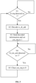
- FIG. 4 is a flowchart of an exemplary implementation solution of a slave device interface module, according to some embodiments of the present disclosure.
- step a1 a received write request signal of a master device is monitored. If it is detected that the received write request signal is valid (e.g., equal to 1), step a2 is performed. If the received write request signal is not valid (e.g., equal to 0), the slave device interface module continuously monitors subsequent received write request signals.
- step a2 after the valid write request signal is detected, a received write address and operation data (w_dt_adr) and request signal (req) are sent to the decoding module, wherein the request signal (req) is set to be valid (e.g., set to 1).
- step a3 the slave interface module monitors whether a valid acknowledgment signal (ack) from the decoding module is received. If it is detected that the valid acknowledgment signal is received and the valid acknowledgment signal (ack) is valid (e.g., equal to 1), the request signal (req) is cleared (e.g., set to 0), and then step a1 is performed. If the valid acknowledgment signal is not valid (e.g., equal to 0), the slave interface module continues to monitor whether a subsequent valid acknowledgment signal is received.
- ack valid acknowledgment signal
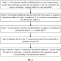
- step 2 after the decoding module receives the write address and operation data (w_dt_adr) and request signal (req), the decoding module decodes the received write address and operation data (w_dt_adr) to generate a destination address C and a bit selection D corresponding to the destination address C.
- the decoding module is responsible for decoding encoded information received from the slave device interface module and sending valid information after the decoding to the master device interface module.
- the mode of implementing the decoding module of the bitwise writing apparatus is superior to the decoding mode of a conventional internal control register. In conventional systems, configuration bit selection control and bit valid data of the internal control register need to occupy instruction space. In the decoding mode of the disclosed bitwise writing apparatus, however, an address, bit selection control, and bit data information are obtained directly by decoding an address and operation data in a current write request of a master control interface of the register. Compared with the conventional decoding mode of configuring the register, the direct decoding mode used by the disclosed bitwise writing apparatus can save the instruction storage space.
- FIG. 5 is flowchart of an exemplary implementation solution of the decoding module, according to some embodiments of the present disclosure.
- step b1 the request signal (req) sent by the slave device interface module is monitored. If the request signal (req) is detected to be valid (e.g., equal to 1), step b2 is performed. If the request signal (req) is not valid (e.g., equal to 0), the decoding module continuously monitors subsequent request signals (req).
- step b2 decoding is performed according to the write address and operation data (w_dt_adr) received from the slave interface module to obtain a destination address C, a bit selection D, and an operand B.
- step b3 the decoding module sends the destination address C, the bit selection D, and the operand B that are obtained in step b2 to the master device interface module.
- the decoding module also sends a read request signal (ym_req) to the master device interface module, wherein the read request signal (ym_req) is set to be valid (e.g., set to 1).
- step b4 the decoding module monitors whether an acknowledgment signal (ym_ack) from the master device interface module is received. If it is detected that the acknowledgment signal (ym_ack) is received and the acknowledgment signal (ym_ack) is valid (e.g., equal to 1), step b5 is performed. If the acknowledgment signal (ym_ack) is not valid (e.g., equal to 0), the decoding module continues to monitor whether a subsequent acknowledgment signal is received.
- step b5 the read request signal (ym_req) is cleared (e.g., set to 0), and then step b1 is performed.
- the decoding module maps the mapping address A into 1) the destination address C, and 2) the bit selection D in the peripheral register corresponding to the destination address C.
- the decoding module then converts the write request information of the master device into peripheral bitwise operation information provided to the master device interface module.
- the decoding mode of the decoding module works as follows: write address and operation data (w_dt_adr) come from both an address signal (w_adr) and a data signal (w_dt) that are received by the slave device interface module.
- the bit selection D comes from a lower bit of the address signal (w_adr) (e.g., if a bus has a 32-bit data width, the bit selection D comes from the lower 5 bits).
- the valid bit for write data can be the lower two bits of the address signal (w_adr), which are used to determine from which bit of the data signal (w_dt) the operand B comes.
- the operand B which represents the bit data information, comes from the bit 0 of the data signal (w_dt). If the lower two bits of the address signal (w_adr) are 1, the operand B comes from the bit 8 of the data signal (w_dt). If the lower two bits of the address signal (w_adr) are 2, the operand B comes from the bit 16 of the data signal (w_dt). If the lower two bits of the address signal (w_adr) are 3, the operand B comes from the bit 24 of the data signal (w_dt).
- step 3 the master device interface module initiates a request to read the destination address C in order to acquire data F.
- step 4 the bit at the D location of data F is replaced with operand B to generate new data G.
- step 5 a request to write the destination address C is initiated and new data G is used as write data, and the new data G is written into the peripheral register corresponding to the destination address C.
- the master device interface module (e.g., master device interface module 13 of FIG. 2 ) first initiates according to the received decoded information a read request to the slave interface of the bus controller to obtain read data.
- the master device interface module then processes the decoded data and the read data according to the decoded information and sends a write request to the slave interface of the bus controller, thereby completing the bitwise write operation.
- FIG. 6 is a flowchart of an exemplary implementation solution of the master device interface module, according to some embodiments of the present disclosure.
- step c1 the master device interface module monitors whether a received read request signal (ym_req) is valid (e.g., equal to 1). If so, step c2 is performed. If, however, the read request signal is not valid (e.g., equal to 0), the master device interface module continues to monitor whether a received read request signal is valid.
- a received read request signal ym_req
- step c2 after it is detected that the read request signal (ym_req) is valid, a read request packet is sent to the bus according to the destination address C obtained by decoding in order to obtain data F.
- step c3 after the read request is completed, a bit at the D location of data F is replaced with operand B to obtain write data G.
- step c4 a request to write data G to the destination address C is sent to the slave device interface of the bus controller.
- step c5 an acknowledgment signal (ym_ack) is set to be valid (e.g., set to 1), and then step c1 is performed.
- ym_ack an acknowledgment signal
- a slave device interface module receives a write request sent by the master device interface of a bus controller and sends received address and data to a decoding module.
- the decoding module decodes the received address and data information and then sends valid information after the decoding to a master device interface module.
- the master device interface module first sends a read request to a slave interface module of the bus controller according to the received decoded information to obtain read data, and then processes the decoded data and the read data according to the decoded information and sends a write request to the slave interface of the bus controller, thus implementing a function of a bitwise write operation.
- embodiments of the present disclosure can directly obtain an address and data of a write request by decoding in a manner that a bitwise write operation of the master device is converted into one write request for implementation, therefore effectively reducing the instruction storage space and lowering the chip cost.
- the program can be stored in a computer readable storage medium.
- the program can comprise processes of the embodiments of the above methods, wherein the storage medium can be a magnetic disk, an optical disc, a Read-Only Memory (ROM), a Random Access Memory (RAM), and the like.
Landscapes
- Engineering & Computer Science (AREA)
- Theoretical Computer Science (AREA)
- General Engineering & Computer Science (AREA)
- Computer Hardware Design (AREA)
- Physics & Mathematics (AREA)
- General Physics & Mathematics (AREA)
- Computing Systems (AREA)
- Microelectronics & Electronic Packaging (AREA)
- Software Systems (AREA)
- Information Transfer Systems (AREA)
- Bus Control (AREA)
Claims (16)
- Bitweises Schreibgerät für ein System-on-Chip-System, wobei das bitweise Schreibgerät kommunikativ an eine Master-Vorrichtungsschnittstelle einer Bussteuerung und eine Slave-Vorrichtungsschnittstelle der Bussteuerung gekoppelt ist und das bitweise Schreibgerät Folgendes umfasst:ein Dekodiermodul, das dazu konfiguriert ist, eine Schreibanforderung von einer Master-Vorrichtung zu empfangen und die Schreibanforderung zu dekodieren, um eine Zieladresse, Bitauswahlinformationen und gültige Bitdaten zu erfassen; undein Master-Vorrichtungsschnittstellenmodul, das zu Folgendem konfiguriert ist:Empfangen der Zieladresse, der Bitauswahlinformationen und der gültigen Bitdaten von dem Dekodiermodul,Lesen von Daten in der Zieladresse, um gelesene Daten zu erhalten;Durchführen einer bitweisen Operation für die gelesenen Daten, um neue Daten gemäß den Bitauswahlinformationen und den gültigen Bitdaten zu erhalten, indem ein zugewiesenes Bit der gelesenen Daten gemäß den Bitauswahlinformationen nach der Dekodierung in die gültigen Bitdaten modifiziert wird, um die neuen Daten zu erhalten, undSenden einer Schreibanforderung an die Slave-Vorrichtungsschnittstelle der Bussteuerung und Schreiben der erhaltenen neuen Daten in ein Peripherieregister, das der Zieladresse entspricht.
- Bitweises Schreibgerät gemäß Anspruch 1, ferner umfassend ein Slave-Vorrichtungsschnittstellenmodul, das dazu konfiguriert ist, eine von der Master-Vorrichtungsschnittstelle der Bussteuerung gesendete Schreibanforderung zu empfangen, wobei die Schreibanforderung eine Zuordnungsadresse und Operationsdaten umfasst.
- Bitweises Schreibgerät gemäß Anspruch 2, wobei das Slave-Vorrichtungsschnittstellenmodul ferner dazu konfiguriert ist, die von der Master-Vorrichtungsschnittstelle der Bussteuerung gesendete Schreibanforderung zu steuern.
- Bitweises Schreibgerät gemäß einem der Ansprüche 2 und 3, wobei die Schreibanforderung ferner eine Bitauswahlsteuerung, eine Steuerung gültiger Bits der Schreibbitdaten und Bitdateninformationen umfasst.
- Bitweises Schreibgerät gemäß einem der Ansprüche 2-4, wobei das Slave-Vorrichtungsschnittstellenmodul ferner dazu konfiguriert ist, ein gültiges Bestätigungssignal von dem Dekodiermodul zu empfangen und zu detektieren.
- Bitweises Schreibgerät gemäß einem der Ansprüche 2-5, wobei das Dekodiermodul ferner dazu konfiguriert ist, die Zuordnungsadresse in der empfangenen Schreibanforderung in eine entsprechende Zieladresse und Bitauswahlinformationen gemäß einer vereinbarten Zuordnungsbeziehung umzuwandeln.
- Bitweises Schreibgerät gemäß einem der Ansprüche 2-6, wobei die Bitauswahlinformationen ein oder mehrere Bits aus den unteren Bits in der Zuordnungsadresse umfassen.
- Bitweises Schreibgerät gemäß einem der Ansprüche 1-7, wobei das Dekodiermodul ferner dazu konfiguriert ist, ein Bestätigungssignal von dem Master-Vorrichtungsschnittstellenmodul zu empfangen und zu detektieren.
- Bitweises Schreibgerät gemäß einem der Ansprüche 1-8, wobei das Master-Vorrichtungsschnittstellenmodul ferner dazu konfiguriert ist, ein Bestätigungssignal an das Dekodiermodul zu senden, nachdem die Schreibanforderung abgeschlossen ist.
- Bitweises Schreibverfahren für ein System-on-Chip-System, umfassendEmpfangen einer Schreibanforderung von einer Master-Vorrichtung;Dekodieren der Schreibanforderung, um eine Zieladresse, Bitauswahlinformationen und gültige Bitdaten zu erfassen;Lesen von Daten in der Zieladresse, um gelesene Daten zu erhalten;Durchführen einer bitweisen Operation für die gelesenen Daten, um neue Daten gemäß den Bitauswahlinformationen und den gültigen Bitdaten zu erhalten, wobei das Durchführen Modifizieren eines zugewiesenen Bits der gelesenen Daten gemäß den Bitauswahlinformationen nach der Dekodierung in die gültigen Bitdaten umfasst, um die neuen Daten zu erhalten;Senden einer Schreibanforderung an eine Slave-Vorrichtung und Schreiben der erhaltenen neuen Daten in ein Peripherieregister, das der Zieladresse entspricht.
- Bitweises Schreibverfahren gemäß Anspruch 10, wobei die Schreibanforderung eine Zuordnungsadresse und Operationsdaten umfasst.
- Bitweises Schreibverfahren gemäß Anspruch 11, wobei das Dekodieren der Schreibanforderung zum Erfassen einer Zieladresse, von Bitauswahlinformationen und gültiger Bitdaten ferner Umwandeln der Zuordnungsadresse in der Schreibanforderung in eine entsprechende Zieladresse und Bitauswahlinformationen gemäß einer vereinbarte Zuordnungsbeziehung umfasst.
- Bitweises Schreibverfahren gemäß Anspruch 10 oder 12, wobei die Schreibanforderung ferner eine Bitauswahlsteuerung, eine Steuerung gültiger Bits der Schreibbitdaten und Bitdateninformationen umfasst.
- Bitweises Schreibverfahren gemäß einem der Ansprüche 10-13, wobei das Dekodieren der Schreibanforderung zum Erfassen einer Zieladresse, von Bitauswahlinformationen und gültiger Bitdaten ferner Senden eines Gültigkeitsbestätigungssignals umfasst.
- Bitweises Schreibverfahren gemäß einem der Ansprüche 10-14, wobei die Bitauswahlinformationen ein oder mehrere Bits aus den unteren Bits in der Zuordnungsadresse umfassen.
- Bitweises Schreibverfahren gemäß einem der Ansprüche 10-15, wobei das Senden einer Schreibanforderung an eine Slave-Vorrichtung und das Schreiben der erhaltenen neuen Daten in ein Peripherieregister, das der Zieladresse entspricht, ferner Senden eines Bestätigungssignals, nachdem die Schreibanforderung abgeschlossen ist.
Applications Claiming Priority (2)
| Application Number | Priority Date | Filing Date | Title |
|---|---|---|---|
| CN201711465004.7A CN108170470A (zh) | 2017-12-28 | 2017-12-28 | Soc系统按位写装置 |
| PCT/CN2018/123486 WO2019128987A1 (en) | 2017-12-28 | 2018-12-25 | Bitwise writing apparatus for system-on-chip system |
Publications (3)
| Publication Number | Publication Date |
|---|---|
| EP3707597A1 EP3707597A1 (de) | 2020-09-16 |
| EP3707597A4 EP3707597A4 (de) | 2021-04-07 |
| EP3707597B1 true EP3707597B1 (de) | 2024-02-28 |
Family
ID=62519289
Family Applications (1)
| Application Number | Title | Priority Date | Filing Date |
|---|---|---|---|
| EP18897840.7A Active EP3707597B1 (de) | 2017-12-28 | 2018-12-25 | Bitweises schreibgerät für system-on-chip-system |
Country Status (5)
| Country | Link |
|---|---|
| US (1) | US10824578B2 (de) |
| EP (1) | EP3707597B1 (de) |
| JP (1) | JP2021508871A (de) |
| CN (1) | CN108170470A (de) |
| WO (1) | WO2019128987A1 (de) |
Families Citing this family (3)
| Publication number | Priority date | Publication date | Assignee | Title |
|---|---|---|---|---|
| CN108170470A (zh) * | 2017-12-28 | 2018-06-15 | 杭州中天微系统有限公司 | Soc系统按位写装置 |
| CN112532207B (zh) * | 2020-11-19 | 2024-01-26 | 浙江集速合芯科技有限公司 | 一种片上可变滤波器快速调谐的方法 |
| CN117118828B (zh) * | 2023-10-23 | 2024-01-23 | 上海芯联芯智能科技有限公司 | 一种协议转换器、电子设备及一种配置方法 |
Family Cites Families (10)
| Publication number | Priority date | Publication date | Assignee | Title |
|---|---|---|---|---|
| US6307789B1 (en) * | 1999-12-28 | 2001-10-23 | Intel Corporation | Scratchpad memory |
| CN102150132A (zh) * | 2008-09-10 | 2011-08-10 | 瑞萨电子株式会社 | 信息处理装置 |
| KR20100063219A (ko) * | 2008-12-03 | 2010-06-11 | 삼성전자주식회사 | 시스템 온 칩에서 비트 단위의 데이터 쓰기 방법 및 장치 |
| CN101477504B (zh) | 2009-02-19 | 2011-07-20 | 浙江中控技术股份有限公司 | 数据传输系统及数据传输方法 |
| KR101620460B1 (ko) | 2010-05-04 | 2016-05-13 | 삼성전자주식회사 | 인터커넥트, 그것을 포함하는 버스 시스템 그리고 버스 시스템의 동작 방법 |
| CN101950279B (zh) * | 2010-09-30 | 2012-09-19 | 华为技术有限公司 | 均衡数据信息流量的方法、总线系统和译码器 |
| CN103605632B (zh) | 2013-11-18 | 2016-06-29 | 山东大学 | 一种axi总线与ahb总线的通信方法与装置 |
| CN106940684B (zh) * | 2016-01-05 | 2020-04-21 | 青岛海信电器股份有限公司 | 一种按比特写数据的方法及装置 |
| US9607682B1 (en) * | 2016-03-28 | 2017-03-28 | Amazon Technologies, Inc. | Address decoding circuit |
| CN108170470A (zh) * | 2017-12-28 | 2018-06-15 | 杭州中天微系统有限公司 | Soc系统按位写装置 |
-
2017
- 2017-12-28 CN CN201711465004.7A patent/CN108170470A/zh active Pending
-
2018
- 2018-12-25 EP EP18897840.7A patent/EP3707597B1/de active Active
- 2018-12-25 WO PCT/CN2018/123486 patent/WO2019128987A1/en not_active Ceased
- 2018-12-25 JP JP2020534266A patent/JP2021508871A/ja active Pending
- 2018-12-25 US US16/479,580 patent/US10824578B2/en active Active
Also Published As
| Publication number | Publication date |
|---|---|
| JP2021508871A (ja) | 2021-03-11 |
| EP3707597A4 (de) | 2021-04-07 |
| US20190370200A1 (en) | 2019-12-05 |
| WO2019128987A1 (en) | 2019-07-04 |
| EP3707597A1 (de) | 2020-09-16 |
| CN108170470A (zh) | 2018-06-15 |
| US10824578B2 (en) | 2020-11-03 |
Similar Documents
| Publication | Publication Date | Title |
|---|---|---|
| TWI684868B (zh) | 記憶體控制器及其操作方法以及記憶體系統之控制方法 | |
| KR100909119B1 (ko) | 집적 dma 엔진을 사용하는 고성능 휘발성 디스크드라이브 메모리 액세스 장치 및 방법 | |
| KR102111741B1 (ko) | 임베디드 멀티미디어 카드 및 이의 동작 방법 | |
| CN105095128B (zh) | 中断处理方法及中断控制器 | |
| US8156376B2 (en) | Method, device and system for storing data in cache in case of power failure | |
| EP3707597B1 (de) | Bitweises schreibgerät für system-on-chip-system | |
| US7689734B2 (en) | Method for toggling non-adjacent channel identifiers during DMA double buffering operations | |
| US7173964B2 (en) | Method for detecting data transmission rate of USB controller by using USB device | |
| CN104021101A (zh) | 基于lpc1768平台的usb接口系统及实现方法 | |
| US7620747B1 (en) | Software based native command queuing | |
| JP2008225577A (ja) | Pciデバイスのホットプラグにおけるモード設定方法及びpciバスを有するシステム | |
| CN102708079B (zh) | 应用于微控制器的控制数据传输的方法及系统 | |
| JP2017045199A (ja) | 制御装置 | |
| CN101739367B (zh) | 多类总线存储控制的方法与装置 | |
| EP4325491A1 (de) | Speichervorrichtung | |
| US7415555B2 (en) | Bus bridge device | |
| KR20240044695A (ko) | 전자 장치 및 그 제어 방법 | |
| US20030018842A1 (en) | Interrupt controller | |
| KR20190058115A (ko) | 대기 모드 전환이 가능한 프린터를 이용하여 인쇄를 수행하는 방법 및 이를 수행하기 위한 장치 | |
| WO2022126398A1 (zh) | 消息通知方法及装置 | |
| US20260037183A1 (en) | Memory controllers, memory systems and control methods thereof, memory mediums, and program products | |
| CN101702133A (zh) | 软件系统管理中断信号处理方法与计算机系统 | |
| US20070088879A1 (en) | Method for initializing bus device | |
| JPH10198524A (ja) | ハードディスク制御装置 | |
| JP5227601B2 (ja) | 制御システム |
Legal Events
| Date | Code | Title | Description |
|---|---|---|---|
| STAA | Information on the status of an ep patent application or granted ep patent |
Free format text: STATUS: THE INTERNATIONAL PUBLICATION HAS BEEN MADE |
|
| PUAI | Public reference made under article 153(3) epc to a published international application that has entered the european phase |
Free format text: ORIGINAL CODE: 0009012 |
|
| STAA | Information on the status of an ep patent application or granted ep patent |
Free format text: STATUS: REQUEST FOR EXAMINATION WAS MADE |
|
| 17P | Request for examination filed |
Effective date: 20200612 |
|
| AK | Designated contracting states |
Kind code of ref document: A1 Designated state(s): AL AT BE BG CH CY CZ DE DK EE ES FI FR GB GR HR HU IE IS IT LI LT LU LV MC MK MT NL NO PL PT RO RS SE SI SK SM TR |
|
| AX | Request for extension of the european patent |
Extension state: BA ME |
|
| RAP1 | Party data changed (applicant data changed or rights of an application transferred) |
Owner name: ALIBABA GROUP HOLDING LIMITED |
|
| A4 | Supplementary search report drawn up and despatched |
Effective date: 20210305 |
|
| DAV | Request for validation of the european patent (deleted) | ||
| DAX | Request for extension of the european patent (deleted) | ||
| RIC1 | Information provided on ipc code assigned before grant |
Ipc: G06F 13/42 20060101ALI20210301BHEP Ipc: G06F 9/30 20180101AFI20210301BHEP Ipc: G06F 15/78 20060101ALI20210301BHEP |
|
| P01 | Opt-out of the competence of the unified patent court (upc) registered |
Effective date: 20230418 |
|
| GRAP | Despatch of communication of intention to grant a patent |
Free format text: ORIGINAL CODE: EPIDOSNIGR1 |
|
| STAA | Information on the status of an ep patent application or granted ep patent |
Free format text: STATUS: GRANT OF PATENT IS INTENDED |
|
| INTG | Intention to grant announced |
Effective date: 20231109 |
|
| GRAS | Grant fee paid |
Free format text: ORIGINAL CODE: EPIDOSNIGR3 |
|
| GRAA | (expected) grant |
Free format text: ORIGINAL CODE: 0009210 |
|
| STAA | Information on the status of an ep patent application or granted ep patent |
Free format text: STATUS: THE PATENT HAS BEEN GRANTED |
|
| AK | Designated contracting states |
Kind code of ref document: B1 Designated state(s): AL AT BE BG CH CY CZ DE DK EE ES FI FR GB GR HR HU IE IS IT LI LT LU LV MC MK MT NL NO PL PT RO RS SE SI SK SM TR |
|
| REG | Reference to a national code |
Ref country code: GB Ref legal event code: FG4D |
|
| REG | Reference to a national code |
Ref country code: CH Ref legal event code: EP |
|
| REG | Reference to a national code |
Ref country code: DE Ref legal event code: R096 Ref document number: 602018066037 Country of ref document: DE |
|
| REG | Reference to a national code |
Ref country code: IE Ref legal event code: FG4D |
|
| REG | Reference to a national code |
Ref country code: LT Ref legal event code: MG9D |
|
| PG25 | Lapsed in a contracting state [announced via postgrant information from national office to epo] |
Ref country code: IS Free format text: LAPSE BECAUSE OF FAILURE TO SUBMIT A TRANSLATION OF THE DESCRIPTION OR TO PAY THE FEE WITHIN THE PRESCRIBED TIME-LIMIT Effective date: 20240628 |
|
| REG | Reference to a national code |
Ref country code: NL Ref legal event code: MP Effective date: 20240228 |
|
| PG25 | Lapsed in a contracting state [announced via postgrant information from national office to epo] |
Ref country code: LT Free format text: LAPSE BECAUSE OF FAILURE TO SUBMIT A TRANSLATION OF THE DESCRIPTION OR TO PAY THE FEE WITHIN THE PRESCRIBED TIME-LIMIT Effective date: 20240228 |
|
| PG25 | Lapsed in a contracting state [announced via postgrant information from national office to epo] |
Ref country code: GR Free format text: LAPSE BECAUSE OF FAILURE TO SUBMIT A TRANSLATION OF THE DESCRIPTION OR TO PAY THE FEE WITHIN THE PRESCRIBED TIME-LIMIT Effective date: 20240529 |
|
| PG25 | Lapsed in a contracting state [announced via postgrant information from national office to epo] |
Ref country code: HR Free format text: LAPSE BECAUSE OF FAILURE TO SUBMIT A TRANSLATION OF THE DESCRIPTION OR TO PAY THE FEE WITHIN THE PRESCRIBED TIME-LIMIT Effective date: 20240228 Ref country code: RS Free format text: LAPSE BECAUSE OF FAILURE TO SUBMIT A TRANSLATION OF THE DESCRIPTION OR TO PAY THE FEE WITHIN THE PRESCRIBED TIME-LIMIT Effective date: 20240528 Ref country code: NL Free format text: LAPSE BECAUSE OF FAILURE TO SUBMIT A TRANSLATION OF THE DESCRIPTION OR TO PAY THE FEE WITHIN THE PRESCRIBED TIME-LIMIT Effective date: 20240228 |
|
| PG25 | Lapsed in a contracting state [announced via postgrant information from national office to epo] |
Ref country code: ES Free format text: LAPSE BECAUSE OF FAILURE TO SUBMIT A TRANSLATION OF THE DESCRIPTION OR TO PAY THE FEE WITHIN THE PRESCRIBED TIME-LIMIT Effective date: 20240228 |
|
| PG25 | Lapsed in a contracting state [announced via postgrant information from national office to epo] |
Ref country code: RS Free format text: LAPSE BECAUSE OF FAILURE TO SUBMIT A TRANSLATION OF THE DESCRIPTION OR TO PAY THE FEE WITHIN THE PRESCRIBED TIME-LIMIT Effective date: 20240528 Ref country code: NO Free format text: LAPSE BECAUSE OF FAILURE TO SUBMIT A TRANSLATION OF THE DESCRIPTION OR TO PAY THE FEE WITHIN THE PRESCRIBED TIME-LIMIT Effective date: 20240528 Ref country code: NL Free format text: LAPSE BECAUSE OF FAILURE TO SUBMIT A TRANSLATION OF THE DESCRIPTION OR TO PAY THE FEE WITHIN THE PRESCRIBED TIME-LIMIT Effective date: 20240228 Ref country code: LT Free format text: LAPSE BECAUSE OF FAILURE TO SUBMIT A TRANSLATION OF THE DESCRIPTION OR TO PAY THE FEE WITHIN THE PRESCRIBED TIME-LIMIT Effective date: 20240228 Ref country code: IS Free format text: LAPSE BECAUSE OF FAILURE TO SUBMIT A TRANSLATION OF THE DESCRIPTION OR TO PAY THE FEE WITHIN THE PRESCRIBED TIME-LIMIT Effective date: 20240628 Ref country code: HR Free format text: LAPSE BECAUSE OF FAILURE TO SUBMIT A TRANSLATION OF THE DESCRIPTION OR TO PAY THE FEE WITHIN THE PRESCRIBED TIME-LIMIT Effective date: 20240228 Ref country code: GR Free format text: LAPSE BECAUSE OF FAILURE TO SUBMIT A TRANSLATION OF THE DESCRIPTION OR TO PAY THE FEE WITHIN THE PRESCRIBED TIME-LIMIT Effective date: 20240529 Ref country code: FI Free format text: LAPSE BECAUSE OF FAILURE TO SUBMIT A TRANSLATION OF THE DESCRIPTION OR TO PAY THE FEE WITHIN THE PRESCRIBED TIME-LIMIT Effective date: 20240228 Ref country code: ES Free format text: LAPSE BECAUSE OF FAILURE TO SUBMIT A TRANSLATION OF THE DESCRIPTION OR TO PAY THE FEE WITHIN THE PRESCRIBED TIME-LIMIT Effective date: 20240228 Ref country code: BG Free format text: LAPSE BECAUSE OF FAILURE TO SUBMIT A TRANSLATION OF THE DESCRIPTION OR TO PAY THE FEE WITHIN THE PRESCRIBED TIME-LIMIT Effective date: 20240228 |
|
| PG25 | Lapsed in a contracting state [announced via postgrant information from national office to epo] |
Ref country code: PT Free format text: LAPSE BECAUSE OF FAILURE TO SUBMIT A TRANSLATION OF THE DESCRIPTION OR TO PAY THE FEE WITHIN THE PRESCRIBED TIME-LIMIT Effective date: 20240628 Ref country code: PL Free format text: LAPSE BECAUSE OF FAILURE TO SUBMIT A TRANSLATION OF THE DESCRIPTION OR TO PAY THE FEE WITHIN THE PRESCRIBED TIME-LIMIT Effective date: 20240228 |
|
| REG | Reference to a national code |
Ref country code: AT Ref legal event code: MK05 Ref document number: 1661855 Country of ref document: AT Kind code of ref document: T Effective date: 20240228 |
|
| PG25 | Lapsed in a contracting state [announced via postgrant information from national office to epo] |
Ref country code: SE Free format text: LAPSE BECAUSE OF FAILURE TO SUBMIT A TRANSLATION OF THE DESCRIPTION OR TO PAY THE FEE WITHIN THE PRESCRIBED TIME-LIMIT Effective date: 20240228 Ref country code: PT Free format text: LAPSE BECAUSE OF FAILURE TO SUBMIT A TRANSLATION OF THE DESCRIPTION OR TO PAY THE FEE WITHIN THE PRESCRIBED TIME-LIMIT Effective date: 20240628 Ref country code: PL Free format text: LAPSE BECAUSE OF FAILURE TO SUBMIT A TRANSLATION OF THE DESCRIPTION OR TO PAY THE FEE WITHIN THE PRESCRIBED TIME-LIMIT Effective date: 20240228 Ref country code: LV Free format text: LAPSE BECAUSE OF FAILURE TO SUBMIT A TRANSLATION OF THE DESCRIPTION OR TO PAY THE FEE WITHIN THE PRESCRIBED TIME-LIMIT Effective date: 20240228 |
|
| PG25 | Lapsed in a contracting state [announced via postgrant information from national office to epo] |
Ref country code: DK Free format text: LAPSE BECAUSE OF FAILURE TO SUBMIT A TRANSLATION OF THE DESCRIPTION OR TO PAY THE FEE WITHIN THE PRESCRIBED TIME-LIMIT Effective date: 20240228 |
|
| PG25 | Lapsed in a contracting state [announced via postgrant information from national office to epo] |
Ref country code: SM Free format text: LAPSE BECAUSE OF FAILURE TO SUBMIT A TRANSLATION OF THE DESCRIPTION OR TO PAY THE FEE WITHIN THE PRESCRIBED TIME-LIMIT Effective date: 20240228 |
|
| PG25 | Lapsed in a contracting state [announced via postgrant information from national office to epo] |
Ref country code: CZ Free format text: LAPSE BECAUSE OF FAILURE TO SUBMIT A TRANSLATION OF THE DESCRIPTION OR TO PAY THE FEE WITHIN THE PRESCRIBED TIME-LIMIT Effective date: 20240228 Ref country code: EE Free format text: LAPSE BECAUSE OF FAILURE TO SUBMIT A TRANSLATION OF THE DESCRIPTION OR TO PAY THE FEE WITHIN THE PRESCRIBED TIME-LIMIT Effective date: 20240228 |
|
| PG25 | Lapsed in a contracting state [announced via postgrant information from national office to epo] |
Ref country code: AT Free format text: LAPSE BECAUSE OF FAILURE TO SUBMIT A TRANSLATION OF THE DESCRIPTION OR TO PAY THE FEE WITHIN THE PRESCRIBED TIME-LIMIT Effective date: 20240228 |
|
| PG25 | Lapsed in a contracting state [announced via postgrant information from national office to epo] |
Ref country code: SK Free format text: LAPSE BECAUSE OF FAILURE TO SUBMIT A TRANSLATION OF THE DESCRIPTION OR TO PAY THE FEE WITHIN THE PRESCRIBED TIME-LIMIT Effective date: 20240228 |
|
| PG25 | Lapsed in a contracting state [announced via postgrant information from national office to epo] |
Ref country code: SM Free format text: LAPSE BECAUSE OF FAILURE TO SUBMIT A TRANSLATION OF THE DESCRIPTION OR TO PAY THE FEE WITHIN THE PRESCRIBED TIME-LIMIT Effective date: 20240228 Ref country code: SK Free format text: LAPSE BECAUSE OF FAILURE TO SUBMIT A TRANSLATION OF THE DESCRIPTION OR TO PAY THE FEE WITHIN THE PRESCRIBED TIME-LIMIT Effective date: 20240228 Ref country code: RO Free format text: LAPSE BECAUSE OF FAILURE TO SUBMIT A TRANSLATION OF THE DESCRIPTION OR TO PAY THE FEE WITHIN THE PRESCRIBED TIME-LIMIT Effective date: 20240228 Ref country code: EE Free format text: LAPSE BECAUSE OF FAILURE TO SUBMIT A TRANSLATION OF THE DESCRIPTION OR TO PAY THE FEE WITHIN THE PRESCRIBED TIME-LIMIT Effective date: 20240228 Ref country code: DK Free format text: LAPSE BECAUSE OF FAILURE TO SUBMIT A TRANSLATION OF THE DESCRIPTION OR TO PAY THE FEE WITHIN THE PRESCRIBED TIME-LIMIT Effective date: 20240228 Ref country code: CZ Free format text: LAPSE BECAUSE OF FAILURE TO SUBMIT A TRANSLATION OF THE DESCRIPTION OR TO PAY THE FEE WITHIN THE PRESCRIBED TIME-LIMIT Effective date: 20240228 Ref country code: AT Free format text: LAPSE BECAUSE OF FAILURE TO SUBMIT A TRANSLATION OF THE DESCRIPTION OR TO PAY THE FEE WITHIN THE PRESCRIBED TIME-LIMIT Effective date: 20240228 |
|
| REG | Reference to a national code |
Ref country code: DE Ref legal event code: R097 Ref document number: 602018066037 Country of ref document: DE |
|
| PG25 | Lapsed in a contracting state [announced via postgrant information from national office to epo] |
Ref country code: IT Free format text: LAPSE BECAUSE OF FAILURE TO SUBMIT A TRANSLATION OF THE DESCRIPTION OR TO PAY THE FEE WITHIN THE PRESCRIBED TIME-LIMIT Effective date: 20240228 |
|
| PG25 | Lapsed in a contracting state [announced via postgrant information from national office to epo] |
Ref country code: IT Free format text: LAPSE BECAUSE OF FAILURE TO SUBMIT A TRANSLATION OF THE DESCRIPTION OR TO PAY THE FEE WITHIN THE PRESCRIBED TIME-LIMIT Effective date: 20240228 |
|
| PLBE | No opposition filed within time limit |
Free format text: ORIGINAL CODE: 0009261 |
|
| STAA | Information on the status of an ep patent application or granted ep patent |
Free format text: STATUS: NO OPPOSITION FILED WITHIN TIME LIMIT |
|
| 26N | No opposition filed |
Effective date: 20241129 |
|
| PG25 | Lapsed in a contracting state [announced via postgrant information from national office to epo] |
Ref country code: SI Free format text: LAPSE BECAUSE OF FAILURE TO SUBMIT A TRANSLATION OF THE DESCRIPTION OR TO PAY THE FEE WITHIN THE PRESCRIBED TIME-LIMIT Effective date: 20240228 |
|
| PG25 | Lapsed in a contracting state [announced via postgrant information from national office to epo] |
Ref country code: MC Free format text: LAPSE BECAUSE OF FAILURE TO SUBMIT A TRANSLATION OF THE DESCRIPTION OR TO PAY THE FEE WITHIN THE PRESCRIBED TIME-LIMIT Effective date: 20240228 |
|
| REG | Reference to a national code |
Ref country code: CH Ref legal event code: PL |
|
| PG25 | Lapsed in a contracting state [announced via postgrant information from national office to epo] |
Ref country code: LU Free format text: LAPSE BECAUSE OF NON-PAYMENT OF DUE FEES Effective date: 20241225 |
|
| REG | Reference to a national code |
Ref country code: BE Ref legal event code: MM Effective date: 20241231 |
|
| PG25 | Lapsed in a contracting state [announced via postgrant information from national office to epo] |
Ref country code: BE Free format text: LAPSE BECAUSE OF NON-PAYMENT OF DUE FEES Effective date: 20241231 |
|
| PG25 | Lapsed in a contracting state [announced via postgrant information from national office to epo] |
Ref country code: CH Free format text: LAPSE BECAUSE OF NON-PAYMENT OF DUE FEES Effective date: 20241231 |
|
| PG25 | Lapsed in a contracting state [announced via postgrant information from national office to epo] |
Ref country code: IE Free format text: LAPSE BECAUSE OF NON-PAYMENT OF DUE FEES Effective date: 20241225 |
|
| PGFP | Annual fee paid to national office [announced via postgrant information from national office to epo] |
Ref country code: DE Payment date: 20251212 Year of fee payment: 8 |
|
| PGFP | Annual fee paid to national office [announced via postgrant information from national office to epo] |
Ref country code: GB Payment date: 20251211 Year of fee payment: 8 |
|
| PGFP | Annual fee paid to national office [announced via postgrant information from national office to epo] |
Ref country code: FR Payment date: 20251212 Year of fee payment: 8 |