EP3706175B1 - Anzeigetafel, bildschirm und anzeigeendgerät - Google Patents
Anzeigetafel, bildschirm und anzeigeendgerät Download PDFInfo
- Publication number
- EP3706175B1 EP3706175B1 EP19846394.5A EP19846394A EP3706175B1 EP 3706175 B1 EP3706175 B1 EP 3706175B1 EP 19846394 A EP19846394 A EP 19846394A EP 3706175 B1 EP3706175 B1 EP 3706175B1
- Authority
- EP
- European Patent Office
- Prior art keywords
- type
- display panel
- display
- separation
- substrate
- Prior art date
- Legal status (The legal status is an assumption and is not a legal conclusion. Google has not performed a legal analysis and makes no representation as to the accuracy of the status listed.)
- Active
Links
Images



Classifications
-
- H—ELECTRICITY
- H10—SEMICONDUCTOR DEVICES; ELECTRIC SOLID-STATE DEVICES NOT OTHERWISE PROVIDED FOR
- H10K—ORGANIC ELECTRIC SOLID-STATE DEVICES
- H10K59/00—Integrated devices, or assemblies of multiple devices, comprising at least one organic light-emitting element covered by group H10K50/00
- H10K59/10—OLED displays
- H10K59/12—Active-matrix OLED [AMOLED] displays
- H10K59/122—Pixel-defining structures or layers, e.g. banks
-
- H—ELECTRICITY
- H10—SEMICONDUCTOR DEVICES; ELECTRIC SOLID-STATE DEVICES NOT OTHERWISE PROVIDED FOR
- H10K—ORGANIC ELECTRIC SOLID-STATE DEVICES
- H10K50/00—Organic light-emitting devices
- H10K50/80—Constructional details
- H10K50/805—Electrodes
- H10K50/81—Anodes
-
- H—ELECTRICITY
- H10—SEMICONDUCTOR DEVICES; ELECTRIC SOLID-STATE DEVICES NOT OTHERWISE PROVIDED FOR
- H10K—ORGANIC ELECTRIC SOLID-STATE DEVICES
- H10K50/00—Organic light-emitting devices
- H10K50/80—Constructional details
- H10K50/805—Electrodes
- H10K50/82—Cathodes
-
- H—ELECTRICITY
- H10—SEMICONDUCTOR DEVICES; ELECTRIC SOLID-STATE DEVICES NOT OTHERWISE PROVIDED FOR
- H10K—ORGANIC ELECTRIC SOLID-STATE DEVICES
- H10K59/00—Integrated devices, or assemblies of multiple devices, comprising at least one organic light-emitting element covered by group H10K50/00
- H10K59/10—OLED displays
- H10K59/12—Active-matrix OLED [AMOLED] displays
- H10K59/128—Active-matrix OLED [AMOLED] displays comprising two independent displays, e.g. for emitting information from two major sides of the display
-
- H—ELECTRICITY
- H10—SEMICONDUCTOR DEVICES; ELECTRIC SOLID-STATE DEVICES NOT OTHERWISE PROVIDED FOR
- H10K—ORGANIC ELECTRIC SOLID-STATE DEVICES
- H10K59/00—Integrated devices, or assemblies of multiple devices, comprising at least one organic light-emitting element covered by group H10K50/00
- H10K59/10—OLED displays
- H10K59/17—Passive-matrix OLED displays
- H10K59/173—Passive-matrix OLED displays comprising banks or shadow masks
-
- H—ELECTRICITY
- H10—SEMICONDUCTOR DEVICES; ELECTRIC SOLID-STATE DEVICES NOT OTHERWISE PROVIDED FOR
- H10K—ORGANIC ELECTRIC SOLID-STATE DEVICES
- H10K59/00—Integrated devices, or assemblies of multiple devices, comprising at least one organic light-emitting element covered by group H10K50/00
- H10K59/10—OLED displays
- H10K59/17—Passive-matrix OLED displays
- H10K59/176—Passive-matrix OLED displays comprising two independent displays, e.g. for emitting information from two major sides of the display
-
- H—ELECTRICITY
- H10—SEMICONDUCTOR DEVICES; ELECTRIC SOLID-STATE DEVICES NOT OTHERWISE PROVIDED FOR
- H10K—ORGANIC ELECTRIC SOLID-STATE DEVICES
- H10K59/00—Integrated devices, or assemblies of multiple devices, comprising at least one organic light-emitting element covered by group H10K50/00
- H10K59/60—OLEDs integrated with inorganic light-sensitive elements, e.g. with inorganic solar cells or inorganic photodiodes
-
- H—ELECTRICITY
- H10—SEMICONDUCTOR DEVICES; ELECTRIC SOLID-STATE DEVICES NOT OTHERWISE PROVIDED FOR
- H10K—ORGANIC ELECTRIC SOLID-STATE DEVICES
- H10K59/00—Integrated devices, or assemblies of multiple devices, comprising at least one organic light-emitting element covered by group H10K50/00
- H10K59/10—OLED displays
- H10K59/12—Active-matrix OLED [AMOLED] displays
- H10K59/1201—Manufacture or treatment
-
- H—ELECTRICITY
- H10—SEMICONDUCTOR DEVICES; ELECTRIC SOLID-STATE DEVICES NOT OTHERWISE PROVIDED FOR
- H10K—ORGANIC ELECTRIC SOLID-STATE DEVICES
- H10K59/00—Integrated devices, or assemblies of multiple devices, comprising at least one organic light-emitting element covered by group H10K50/00
- H10K59/60—OLEDs integrated with inorganic light-sensitive elements, e.g. with inorganic solar cells or inorganic photodiodes
- H10K59/65—OLEDs integrated with inorganic image sensors
-
- H—ELECTRICITY
- H10—SEMICONDUCTOR DEVICES; ELECTRIC SOLID-STATE DEVICES NOT OTHERWISE PROVIDED FOR
- H10K—ORGANIC ELECTRIC SOLID-STATE DEVICES
- H10K59/00—Integrated devices, or assemblies of multiple devices, comprising at least one organic light-emitting element covered by group H10K50/00
- H10K59/80—Constructional details
- H10K59/805—Electrodes
- H10K59/8051—Anodes
-
- H—ELECTRICITY
- H10—SEMICONDUCTOR DEVICES; ELECTRIC SOLID-STATE DEVICES NOT OTHERWISE PROVIDED FOR
- H10K—ORGANIC ELECTRIC SOLID-STATE DEVICES
- H10K59/00—Integrated devices, or assemblies of multiple devices, comprising at least one organic light-emitting element covered by group H10K50/00
- H10K59/80—Constructional details
- H10K59/805—Electrodes
- H10K59/8052—Cathodes
Definitions
- the present disclosure relates to display technologies, and more particularly relates to a display panel, a display screen, and a display terminal.
- US 2002/060518 A1 discloses an electroluminescent (EL) device comprising a first and a second electrode layer, at least the second electrode layer being provided in accordance with a desired pattern and one or more functional layers, the one or at least one of said functional layers being an electroluminescent layer.
- the EL device comprises a relief pattern having one or more overhanging sections.
- the EL device has means for hindering the transport of fluid along a capillary channel formed by an overhanging section and the surface supporting that section, an example of such means being protrusions which block and/or reroute the capillary channel.
- US 2015/090991 A1 discloses a filling material provided in an interval part between a first substrate provided with a light emitting device in a pixel and a second substrate provided with a color filter layer corresponding to each pixel which is provided to face each other and a protruding part is provided in the interval part.
- the protruding part is provided separated along one edge of each pixel.
- An end part in a length direction of the protruding part is formed in a cone or streamlined shape.
- the protruding part is formed from a material having light absorbing properties such as carbon black so as to provide light shielding properties.
- KR20160005238 A discloses an organic light emitting diode display device comprising banks having periodically shaped concave-convex side walls.
- Exemplary embodiments of the present disclosure provide a display panel, a display screen, and a display terminal.
- a display panel includes a substrate, a first pixel electrode disposed on the substrate, a pixel definition layer disposed on a side of the first pixel electrode away from the substrate, and a plurality of first type of separation pillars disposed on the pixel definition layer.
- the pixel definition layer includes a plurality of pixel openings to expose a portion of a surface of the first pixel electrode.
- a width of one of the first type of separation pillars changes continuously or intermittently in an extending direction of one of the first type of separation pillars.
- the extending direction of one of the first type of separation pillars is parallel to the substrate.
- the width is a dimension of a projection of one of the first type of separation pillars on the substrate in a direction perpendicular to the extending direction of one of the first type of separation pillars. Furthermore, the width periodically changes along the extending direction, one width changing period of the plurality of first type of separation pillars corresponding to one sub-pixel area.
- the plurality of first type of separation pillars has a bottom surface in contact with the pixel definition layer and a top surface positioned opposite to the bottom surface.
- a width of the top surface is greater than or equal to a width of the bottom surface and the top surface has a changing width along the extending direction of one of the first type of separation pillars.
- at least one of two side edges of the top surface of one of the first type of separation pillars along the extending direction of one of the first type of separation pillars has a shape of at least one of an arc and a semicircle.
- the plurality of the first type of separation pillars is arranged in parallel on the substrate.
- the first pixel electrode is made of at least one selected from the group consisting of indium tin oxide, indium zinc oxide, silver-doped indium tin oxide, and silver-doped indium zinc oxide.
- the display panel further comprises a plurality of second type of separation pillars, wherein one of the second type of separation pillars has a strip shape, and the first type of separation pillars and the second type of separation pillars are disposed alternately.
- the bottom surface is parallel to the top surface, and a shape of the bottom surface is substantially the same as a shape of the top surface.
- the plurality of first type of separation pillars further comprises two side surfaces connected to the top surface and the bottom surface, and a projection of each of the side surfaces on the substrate coincides with a projection of the side edge on the substrate.
- the shape of the side edge is formed by connecting a plurality of semicircular edges having the same opening direction, and one of the edges has an opening facing a sub-pixel area.
- a projection of one of the pixel openings on the substrate is a pattern unit or at least two pattern units connected to one another, and the pattern unit has a circular shape, elliptical shape, or dumbbell shape.
- the display panel further comprises a light emitting structure layer disposed on a side of the first pixel electrode away from the substrate and a second pixel electrode disposed on a side of the light emitting structure layer away from the first pixel electrode; an extending direction of the first pixel electrode being perpendicular to an extending direction of the second pixel electrode; wherein preferably the second pixel electrode is made of at least one selected from the group consisting of indium tin oxide, indium zinc oxide, silver-doped indium tin oxide, and silver-doped indium zinc oxide.
- a display screen includes a first display area and the aforementioned display panel.
- the first display area is configured to display a picture.
- the display panel is disposed in the first display area.
- the display screen further comprises a second display area adjacent to the first display area, and a second display panel disposed on the second display area, the display panel being a passive-matrix organic light-emitting diode, PMOLED, display panel or an active-matrix organic light-emitting diode, AMOLED, display panel, and the second display panel being an AMOLED display panel.
- a light transmittance of the first display area is greater than a light transmittance of the second display area; or a light transmittance of the first display area is the same as a light transmittance of the second display area.
- a display terminal includes a device body and the aforementioned display screen.
- the device body has a device area.
- the display screen is disposed on the device body.
- the device area is located under the first display area and a photosensitive device is disposed in the device area; wherein preferably the device area is a notched area, and the photosensitive device comprises a camera or a light sensor.
- orientation or position relationships that are indicated by the terms “center”, “transverse”, “on”, “under”, “left”, “right”, “vertical”, “horizontal”, “top”, “bottom”, “inside”, and “outside”, and the like are orientation or position relationships shown based on the accompany drawings, and are merely for convenience of the description of the present disclosure and simplifying description, rather than indicating or implying that the indicated device or element must have a particular orientation or being constructed and operated in a particular orientation, and are therefore not to be construed as limitation of the present disclosure.
- the terms “first”, “second”, and the like are used for descriptive purposes only, and cannot be understood to indicate or imply relative importance or implicitly indicate the number of technical features indicated. Therefore, the defined “first” and “second” features may explicitly or implicitly include one or more of the features.
- the inventors have found that when a photosensitive device such as a camera or the like is placed under a transparent display panel, the taken photos are blurred.
- the inventors have found after research that this problem is due to the presence of conductive traces in the display screen body of electronic devices. External light can generate diffraction phenomenon when passing through these conductive traces, and the diffraction intensity distribution is more complex, resulting in diffraction fringes, which would then affect the normal operation of the photosensitive device such as a camera or the like.
- external light can be obviously diffracted after passing through the wire material traces in the display screen, so that the picture captured by the camera is distorted.
- FIG. 1 is a cross-sectional view of a display panel in accordance with an exemplary embodiment.
- the display panel includes a substrate 110, a first pixel electrode 120, a pixel definition layer 130, and a separation pillar 140.
- the substrate 110 may be a rigid substrate or a flexible substrate.
- the rigid substrate may be a transparent substrate such as a glass substrate, a quartz substrate, a plastic substrate or the like
- the flexible substrate may be a flexible polyimide (PI) substrate or the like.
- the first pixel electrode 120 is formed on a substrate 110. There is a plurality of first pixel electrodes 120 arranged regularly on the substrate 110. In the present embodiment, one side of the substrate 110 on which the first pixel electrode 120 is formed is an upper side, and the opposite side thereof is a lower side.
- the display panel is a passive-matrix organic light-emitting diode (PMOLED) display panel.
- PMOLED passive-matrix organic light-emitting diode
- each conductive trace of the display panel, such as the first pixel electrode 120 is made of a transparent conductive metal oxide.
- the first pixel electrode 120 may be made of indium tin oxide (ITO) or indium zinc oxide (IZO).
- the first pixel electrode 120 may also be made of materials such as aluminum-doped zinc oxide, silver-doped ITO, silver-doped IZO or the like.
- the aforementioned display panel further includes a light emitting structure layer 150 formed on the first pixel electrode 120 and a second pixel electrode 160 formed on the light emitting structure layer 150.
- the second pixel electrode 160 may be made of a transparent conductive metal oxide.
- the second pixel electrode 160 may be made of indium tin oxide (ITO) or indium zinc oxide (IZO).
- ITO indium tin oxide
- IZO indium zinc oxide
- the second pixel electrode 160 may also be made of materials such as aluminum-doped zinc oxide, silver-doped ITO, silver-doped IZO or the like.
- the first pixel electrode 120 is an anode
- the second pixel electrode 160 is a cathode.
- the pixel definition layer 130 is formed on the first pixel electrode 120.
- the pixel definition layer 130 has a plurality of pixel openings 132 to expose a portion of the surface of the first pixel electrode 120. Each of the pixel openings 132 is used to define a sub-pixel area.
- the separation pillar 140 is formed on the pixel definition layer 130 and is disposed between two adjacent first pixel electrodes 120. The separation pillar 140 is used to separate the cathodes of two adjacent sub-pixel areas, as shown in FIG. 1 . The surface of the separation pillar 140 is higher than the surface of the adjacent sub-pixel area.
- the separation cathode 160b formed above the separation pillar 140 is disconnected from the cathode (the second pixel electrode 160) on the adjacent sub-pixel area, thereby achieving separation of the cathodes of the adjacent sub-pixel areas, and finally ensuring that each sub-pixel area can be normally driven. That is, the shape of the cathode is defined by a gap between adjacent separation pillars 140 and is complementary to the shape of the top surface of the separation pillar 140 to form a whole-surface structure.
- FIG. 2 is a top view of a first type of separation pillar in accordance with an exemplary embodiment.
- the separation pillar 140 includes a first type of separation pillar 140a.
- a width of the first type of separation pillar 140a changes continuously in an extending direction thereof.
- Diffraction phenomenon occurs when external light passes through the separation pillar.
- Diffraction is a physical phenomenon in which a light wave propagates away from an original straight line when encountering an obstacle. Specifically, light waves propagate with varying degrees of bending and spreading after passing through obstacles such as slits, small holes, disks, or the like.
- obstacles such as slits, small holes, disks, or the like.
- a conventional separation pillar is generally in a strip shape, and has an inverted trapezoidal structure in a longitudinal section (i.e., a section perpendicular to the substrate 110).
- the separation pillar has a bottom surface in contact with the substrate 110 and a top surface opposite to the bottom surface.
- the separation pillar is tapered from the top surface to the bottom surface such that the maximum width of the separation pillar appears on the top surface.
- the top surface is rectangular and has a constant width along the extending direction (that is, the width is the same in each position along the extending direction, which is the direction parallel to the substrate 110).
- the diffraction fringes generated at the position with the same width on the separation pillars have the same position, so that the diffraction effect is more obvious, and the normal operation of the photosensitive element located below the separation pillars is influenced finally, for example, the picture captured by the camera is distorted.
- the first type of separation pillars whose widths change continuously or intermittently in the extending direction are used, and the diffraction fringes with different positions are generated at positions of different maximum widths, so that the complex diffraction intensity distribution caused by the conventional separation pillars can be destroyed, the diffraction is relatively less obvious, and the effect of improving the diffraction is achieved.
- the first type of separation pillars 140 there may be a plurality of the first type of separation pillars 140.
- the plurality of first type of separation pillars 140a is arranged in parallel on the substrate 110.
- the first type of separation pillar 140a has a width within 5 ⁇ m to 100 ⁇ m.
- the minimum width of the first type of separation pillar 140a depends on the manufacturing process. Under the premise that the manufacturing process can be achieved, the width of the first type of separation pillar 140a can be less than or equal to 5 ⁇ m, or even less.
- a distance between two adjacent first type of separation pillars 140a depends on the design requirements of the dimension of the cathodes of two adjacent sub-pixel areas.
- the diffraction effect at various positions of the display panel can be uniformly improved, and the purpose of improving the diffraction effect of the display panel as a whole is achieved.
- the separation pillar 140 includes a bottom surface 142 in contact with the substrate 110 and a top surface 144 opposite to the bottom surface 142.
- the top surface 144 in a longitudinal section of the separation pillar 140, has a width greater than or equal to the width of the bottom surface 142.
- the maximum width of the separation pillar 140 is located on the top surface 144, that is, the separation pillars 140 are tapered along the top surface 144 to the bottom surface 142 in a height direction. Therefore, the top surface 144 has a continuously changing width or an intermittently changing width along the extending direction.
- the bottom surface 142 of the separation pillar 140 is disposed parallel to the top surface 144, and the width of the bottom surface 142 is equal to or less than the width of the top surface 144 in the same cross section, so that the entire separation pillar 140 has a structure with a larger top and a smaller bottom.
- the bottom surface 142 has substantially the same shape as the top surface 144, thereby ensuring that the separation pillars 140 have a continuously changing width or an intermittently changing width in the extending direction on any plane parallel to the substrate 110 (that is, at different height positions of the separation pillars 140), so as to ensure that no obvious diffraction effect is generated after light passes through the separation pillars 140.
- the first type of separation pillar 140a has a periodically changing width along its own extending direction.
- the width of the first type of separation pillar 140a does not change irregularly but changes regularly and periodically, so that the difficulty of the entire manufacturing process can be reduced.
- one width changing period of the first type of separation pillar 140a corresponds to one sub-pixel area.
- At least one of two side edges of the top surface of the first type of separation pillar along the extending direction has a non-linear shape.
- the non-linear shape is at least one of an arc and a semicircle.
- the non-linear shape is formed by connecting a plurality of semicircular edges having the same opening direction.
- a semicircular opening is disposed towards the sub-pixel area 130a to reduce the influence on the pixel, and ensure the aperture ratio of the pixel while ensuring the brightness thereof to meet the requirements.
- the size of the diameter of the semicircle depends on the size of the pixel. The larger the pixel, the larger the diameter of the semicircle, and the smaller the pixel, the smaller the diameter of the semicircle.
- the minimum width of the top surface is determined by process limit capabilities.
- the adoption of the semicircular non-linear shape can lead the diffraction fringes not to be diffused towards one direction like the conventional strip-shaped separation pillar but to be diffused towards 360 degrees, thereby making the diffraction extremely unobvious and having better diffraction improvement effect.
- the edge area of the top surface corresponding to the pixel area is set to be semicircular, so that the influence on the pixel is minimum, the aperture ratio of the pixel is higher, and the brightness is higher.
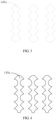
- FIG. 3 is a top view of an exemplary first type of separation pillar 140a, that is, a schematic view of the top surface thereof, which does not form part of the invention.
- the non-linear shape is formed by connecting the edges of a plurality of polyline segments, so that the first type of separation pillar is ensured to have a changing width along the extending direction, and the diffraction effect is improved.
- the opening of each of the polyline segments is disposed towards the sub-pixel area to reduce the influence on the pixel, and ensure the aperture ratio of the pixel while ensuring the brightness thereof to meet the requirements.
- the polyline segment corresponding to each of the pixel areas may also be formed by more polyline segments, thereby forming a jagged edge.
- the side edge of the non-linear shape may also be in the shape of an ellipse or the like, or as shown in FIG. 4 , the side edge of the non-linear shape is formed in an irregular shape formed by line segments and arcs alternately, and it is only necessary to ensure that the first type of separation pillar 140a has a changing width along the length direction, thereby ensuring that the slit diffraction caused by the conventional strip-shaped separation pillar can be destroyed and the effect of improving the diffraction can be achieved.
- the separation pillar 140 further includes two side surfaces 146 connected to the bottom surface 142 and the top surface 144.
- a projection of each of the side surfaces 146 on the substrate 110 coincides with a projection of the side edge of the top surface 144 on the substrate 110.
- the shape of the side surface 146 depends on the shape of the side edge of the top surface 144 and the shape of the side edge of the bottom surface 142.
- the side surface 146 is formed by connecting a plurality of planes at a certain angle.
- the side surface 146 is formed by connecting a plurality of arc surfaces, and a radius of curvature of the arc surface is the same as the diameter of the semicircle of the side edge of the top surface 144.
- the edges of pixel openings 132 in the pixel definition layer 130 are curved and are not parallel to each other.
- the projection of the pixel opening 132 on the substrate 110 is one pattern unit or formed by connecting two or more pattern units.
- the pattern unit has a circular shape, elliptical shape, or dumbbell shape.
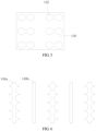
- FIG. 5 is a schematic view of a pixel definition layer 130 in accordance with an exemplary embodiment, on which a dumbbell-shaped pixel opening 132 is formed.
- the separation pillar 140 further includes a second type of separation pillar 140b.
- the second type of separation pillar 140b has a strip shape.
- the second type of separation pillar 140b has a rectangular top surface and has an inverted trapezoidal structure in a longitudinal section.
- the first type of separation pillars 140a and the second type of separation pillars 140b are disposed alternately, as shown in FIG. 6 .
- the separation pillars in the display panel are all first type of separation pillars 140a.
- the slit diffraction fringes generated by each of the first type of separation pillars 140a in different widths have different positions, so that the diffraction is less obvious, and a better effect of improving diffraction is achieved.
- the display panel may be a transparent or transflective display panel.
- the transparency of the display panel can be achieved by using various layers of materials with better light transmittance.
- each layer of the display panel is made of a material having a light transmittance of greater than 90%, so that the light transmittance of the entire display panel may be greater than 70%.
- each layer of the display panel is made of a material having a light transmittance of greater than 95%, so that the light transmittance of the display panel is further improved, and even the light transmittance of the entire display panel is greater than 80%.
- the conductive traces such as the cathode and the anode may be made of ITO, IZO, Ag + ITO, or Ag + IZO, etc.
- an insulating layer is preferably made of SiO 2 , SiN x , Al 2 O 3 , etc.
- the pixel definition layer 130 is made of a highly transparent material.
- the transparent or transflective display panel can display the picture normally when it is in an operation state.
- external light can irradiate the photosensitive device and the like disposed under the display panel through the display panel.
- FIG. 7 is a schematic view of a display screen in accordance with an embodiment, and the display screen includes a first display area 910 and a second display area 920.
- a light transmittance of the first display area 910 is greater than a light transmittance of the second display area 920.
- a photosensitive device 930 may be disposed under the first display area 910.
- a first display panel is disposed in the first display area 910.
- the first display panel is a display panel as mentioned in any of the foregoing embodiments.
- a second display panel is disposed in the second display area 920. Both the first display area 910 and the second display area 920 are used to display a static or dynamic picture.
- the display panel in the foregoing embodiments is adopted in the first display area 910, when light passes through the display area, no obvious diffraction effect is generated, so that the photosensitive device 930 located under the first display area 910 can be ensured to work normally.
- the first display area 910 may display dynamic or static pictures normally when the photosensitive device 930 is not in operation, and the first display area 910 may be in a non-display state when the photosensitive device 930 is in operation, thereby ensuring that the photosensitive device 930 can perform light collection normally through the display panel.
- the light transmittance of the first display area 910 may also be the same as the light transmittance of the second display area 920, so that the entire display panel has better light transmittance uniformity, ensuring a better display effect of the display panel.
- the first display panel disposed in the first display area 910 is a PMOLED display panel or an active-matrix organic light-emitting diode (AMOLED) display panel
- the second display panel disposed in the second display area 920 is an AMOLED display panel, thereby forming a full screen composed of a PMOLED display panel and an AMOLED display panel.
- AMOLED active-matrix organic light-emitting diode
- FIG. 8 is a schematic view of a display terminal in accordance with an embodiment, and the display terminal includes a device body 810 and a display screen 820.
- the display screen 820 is disposed on the device body 810 and is interconnected with the device body 810.
- the display screen 820 may use a display screen in any of the foregoing embodiments to display a static or dynamic picture.
- FIG. 9 is a schematic view of the device body 810 in accordance with an embodiment.
- the device body 810 may be provided with a notched area 812 and a non-notched area 814.
- Photosensitive devices such as cameras 930, optical sensors, and the like may be disposed in the notched area 812.
- the display panel in the first display area of the display screen 820 is correspondingly attached to the notched area 814, so that the aforementioned photosensitive devices such as the camera 930, the optical sensor, and the like can perform operations such as external light collection and the like through the first display area.
- the display panel in the first display area can effectively improve the diffraction phenomenon generated by the transmission of the external light through the first display area, the quality of the image captured by the camera 930 on the display device can be effectively improved, the distortion of the captured image caused by diffraction can be avoided, and the accuracy and the sensitivity of the optical sensor to sense external light can also be improved.
- the aforementioned electronic device may be a digital device such as a mobile phone, a tablet, a palmtop computer, an ipod, and the like.
Landscapes
- Engineering & Computer Science (AREA)
- Microelectronics & Electronic Packaging (AREA)
- Chemical & Material Sciences (AREA)
- Inorganic Chemistry (AREA)
- Physics & Mathematics (AREA)
- Optics & Photonics (AREA)
- Life Sciences & Earth Sciences (AREA)
- Sustainable Development (AREA)
- Manufacturing & Machinery (AREA)
- Electroluminescent Light Sources (AREA)
- Devices For Indicating Variable Information By Combining Individual Elements (AREA)
Claims (13)
- Anzeigefeld, umfassend:ein Substrat (110);eine erste Pixelelektrode (120), die auf dem Substrat (110) eingerichtet ist;eine Pixeldefinitionsschicht (130), die auf einer Seite der ersten Pixelelektrode (120) von dem Substrat (110) weg eingerichtet ist, und umfassend eine Vielzahl von Pixelöffnungen (132) um einen Abschnitt einer Oberfläche der ersten Pixelelektrode (120) freizulegen; undeine Vielzahl von Trennsäulen (140a) des ersten Typs, die auf einer Seite der Pixeldefinitionsschicht (130) von der ersten Pixelelektrode (120) weg eingerichtet ist, wobei sich eine Breite einer der Trennsäulen (140a) des ersten Typs kontinuierlich oder intermittierend in einer Erstreckungsrichtung einer der Trennsäulen (140a) des ersten Typs ändert, und die Erstreckungsrichtung einer der Trennsäulen (140a) des ersten Typs parallel zu dem Substrat (110) ist;wobei die Breite eine Abmessung einer Projektion einer der Trennsäulen (140a) des ersten Typs auf dem Substrat (110) in einer Richtung senkrecht zu der Erstreckungsrichtung einer der Trennsäulen (140a) des ersten Typs ist;wobei sich die Breite entlang der Erstreckungsrichtung periodisch ändert, wobei eine Breitenänderungsperiode der Vielzahl von Trennsäulen (140a) des ersten Typs einem Subpixelbereich entspricht;wobeidie Vielzahl der Trennsäulen (140a) des ersten Typs eine untere Oberfläche (142) in Kontakt mit der Pixeldefinitionsschicht (130) und eine obere Oberfläche (144), die gegenüber der unteren Oberfläche (142) positioniert ist, aufweist;wobei in der Richtung senkrecht zu der Erstreckungsrichtung einer der Trennsäulen (140a) des ersten Typs eine Breite der oberen Oberfläche (144) größer als oder gleich einer Breite der unteren Oberfläche (142) ist; undund wobeidie obere Oberfläche (144) eine sich ändernde Breite entlang der Erstreckungsrichtung einer der Trennsäulen (140a) des ersten Typs aufweist;dadurch gekennzeichnet, dassmindestens eine der zwei Seitenkanten der oberen Oberfläche (144) einer der Trennsäulen (140a) des ersten Typs entlang der Erstreckungsrichtung einer der Trennsäulen (140a) des ersten Typs die Form eines Bogens oder eines Halbkreises aufweist.
- Anzeigefeld nach Anspruch 1, wobei die Vielzahl der Trennsäulen (140a) des ersten Typs parallel auf dem Substrat (110) angeordnet ist.
- Anzeigefeld nach Anspruch 1, wobei die erste Pixelelektrode (120) aus mindestens einem Material hergestellt ist, das aus der Gruppe ausgewählt ist, bestehend aus Indiumzinnoxid, Indiumzinkoxid, silberdotiertem Indiumzinnoxid und silberdotiertem Indiumzinkoxid.
- Anzeigefeld nach Anspruch 1, ferner umfassend eine Vielzahl von Trennsäulen (140b) des zweiten Typs, wobei eine der Trennsäulen (140b) des zweiten Typs eine Streifenform aufweist und die Trennsäulen (140a) des ersten Typs und die Trennsäulen (140b) des zweiten Typs abwechselnd eingerichtet sind.
- Anzeigefeld nach Anspruch 1, wobei die untere Oberfläche (142) parallel zu der oberen Oberfläche (144) ist und ein Form der unteren Oberfläche (142) im Wesentlichen die gleiche wie eine Form der oberen Oberfläche (144) ist.
- Anzeigefeld nach Anspruch 1, wobei die Vielzahl der Trennsäulen (140a) des ersten Typs ferner zwei Seitenoberflächen (146) umfasst, die mit der oberen Oberfläche (144) und der unteren Oberfläche (142) verbunden sind, und eine Projektion jeder der Seitenoberflächen (146) auf dem Substrat (110) mit einer Projektion der Seitenkante auf dem Substrat (110) übereinstimmt.
- Anzeigefeld nach Anspruch 1, wobei die Form der Seitenkante durch Verbinden einer Vielzahl von halbkreisförmigen Kanten, die dieselbe Öffnungsrichtung aufweisen, ausgebildet wird und eine der Kanten eine Öffnung aufweist, die einem Subpixelbereich (130a) zugewandt ist.
- Anzeigefeld nach Anspruch 1, wobei eine Projektion einer der Pixelöffnungen (132) auf dem Substrat (110) eine Mustereinheit oder mindestens zwei miteinander verbundene Mustereinheiten ist und die Mustereinheit eine Kreisform, eine Ellipsenform oder eine Hantelform aufweist.
- Anzeigefeld nach Anspruch 1, ferner umfassend eine Licht emittierende Strukturschicht (150), die auf einer Seite der ersten Pixelelektrode (120) von dem Substrat (110) weg eingerichtet ist, und eine zweite Pixelelektrode (160), die auf einer Seite der Licht emittierenden Strukturschicht (150) von der ersten Pixelelektrode (120) weg eingerichtet ist; wobei eine Erstreckungsrichtung der ersten Pixelelektrode (120) senkrecht zu einer Erstreckungsrichtung der zweiten Pixelelektrode (160) ist.
- Anzeigebildschirm (820), umfassend:einen ersten Anzeigebereich (910), der konfiguriert ist, um ein Bild anzuzeigen; unddas Anzeigefeld nach einem der Ansprüche 1 bis 9, das in dem ersten Anzeigebereich (910) eingerichtet ist.
- Anzeigebildschirm (820) nach Anspruch 10, ferner umfassend einen zweiten Anzeigebereich (920) angrenzend an den ersten Anzeigebereich (910) und ein zweites Anzeigefeld, das auf dem zweiten Anzeigebereich (920) eingerichtet ist, wobei das Anzeigefeld ein Anzeigefeld mit organischen Leuchtdioden mit passiver Matrix (PMOLED) oder ein Anzeigefeld mit organischen Leuchtdioden mit aktiver Matrix (AMOLED) ist, und wobei das zweite Anzeigefeld ein AMOLED-Anzeigefeld ist.
- Anzeigebildschirm (820) nach Anspruch 11, wobei eine Lichtdurchlässigkeit des ersten Anzeigebereichs (910) größer als eine Lichtdurchlässigkeit des zweiten Anzeigebereichs (920) ist; oder
eine Lichtdurchlässigkeit des ersten Anzeigebereichs (910) gleich einer Lichtdurchlässigkeit des zweiten Anzeigebereichs (920) ist. - Anzeigeendgerät, umfassend:einen Vorrichtungskörper (810), der einen Vorrichtungsbereich aufweist; undden Anzeigebildschirm (820) nach Anspruch 10, der auf dem Vorrichtungskörper (810) eingerichtet ist;wobei sich der Vorrichtungsbereich unter dem ersten Anzeigebereich (910) befindet und eine lichtempfindliche Vorrichtung (930) in dem Vorrichtungsbereich eingerichtet ist.
Applications Claiming Priority (2)
| Application Number | Priority Date | Filing Date | Title |
|---|---|---|---|
| CN201810887652.XA CN110767677B (zh) | 2018-08-06 | 2018-08-06 | 显示面板、显示屏及显示终端 |
| PCT/CN2019/085577 WO2020029621A1 (zh) | 2018-08-06 | 2019-05-05 | 显示面板、显示屏及显示终端 |
Publications (3)
| Publication Number | Publication Date |
|---|---|
| EP3706175A1 EP3706175A1 (de) | 2020-09-09 |
| EP3706175A4 EP3706175A4 (de) | 2021-04-21 |
| EP3706175B1 true EP3706175B1 (de) | 2024-11-06 |
Family
ID=69328516
Family Applications (1)
| Application Number | Title | Priority Date | Filing Date |
|---|---|---|---|
| EP19846394.5A Active EP3706175B1 (de) | 2018-08-06 | 2019-05-05 | Anzeigetafel, bildschirm und anzeigeendgerät |
Country Status (6)
| Country | Link |
|---|---|
| US (1) | US10903303B2 (de) |
| EP (1) | EP3706175B1 (de) |
| JP (1) | JP6912668B2 (de) |
| KR (1) | KR102394880B1 (de) |
| CN (1) | CN110767677B (de) |
| WO (1) | WO2020029621A1 (de) |
Families Citing this family (19)
| Publication number | Priority date | Publication date | Assignee | Title |
|---|---|---|---|---|
| CA3002752A1 (en) | 2015-10-26 | 2017-05-04 | Oti Lumionics Inc. | Method for patterning a coating on a surface and device including a patterned coating |
| KR102802931B1 (ko) | 2016-12-02 | 2025-05-08 | 오티아이 루미오닉스 인크. | 방출 영역 위에 배치된 전도성 코팅을 포함하는 디바이스 및 이를 위한 방법 |
| KR102563713B1 (ko) | 2017-04-26 | 2023-08-07 | 오티아이 루미오닉스 인크. | 표면의 코팅을 패턴화하는 방법 및 패턴화된 코팅을 포함하는 장치 |
| CN110832660B (zh) | 2017-05-17 | 2023-07-28 | Oti照明公司 | 在图案化涂层上选择性沉积传导性涂层的方法和包括传导性涂层的装置 |
| US11751415B2 (en) | 2018-02-02 | 2023-09-05 | Oti Lumionics Inc. | Materials for forming a nucleation-inhibiting coating and devices incorporating same |
| US11489136B2 (en) | 2018-05-07 | 2022-11-01 | Oti Lumionics Inc. | Method for providing an auxiliary electrode and device including an auxiliary electrode |
| CN110767674B (zh) * | 2018-08-06 | 2022-05-17 | 苏州清越光电科技股份有限公司 | 显示面板、显示屏及显示终端 |
| JP2022508040A (ja) | 2018-11-23 | 2022-01-19 | オーティーアイ ルミオニクス インコーポレーテッド | 光透過領域を含むオプトエレクトロニクスデバイス |
| CN111384284B (zh) * | 2018-12-29 | 2021-06-25 | 武汉华星光电半导体显示技术有限公司 | 显示面板、电子设备及显示面板的制作方法 |
| KR20250160226A (ko) | 2019-03-07 | 2025-11-11 | 오티아이 루미오닉스 인크. | 핵생성 억제 코팅물 형성용 재료 및 이를 포함하는 디바이스 |
| JP7555600B2 (ja) | 2019-04-18 | 2024-09-25 | オーティーアイ ルミオニクス インコーポレーテッド | 核生成抑制コーティングを形成するための材料およびそれを組み込んだデバイス |
| JP7576337B2 (ja) | 2019-05-08 | 2024-11-01 | オーティーアイ ルミオニクス インコーポレーテッド | 核生成抑制コーティングを形成するための材料およびそれを組み込んだデバイス |
| US11832473B2 (en) | 2019-06-26 | 2023-11-28 | Oti Lumionics Inc. | Optoelectronic device including light transmissive regions, with light diffraction characteristics |
| KR20240134240A (ko) | 2019-06-26 | 2024-09-06 | 오티아이 루미오닉스 인크. | 광 회절 특성을 갖는 광 투과 영역을 포함하는 광전자 디바이스 |
| KR102818817B1 (ko) | 2019-08-09 | 2025-06-11 | 오티아이 루미오닉스 인크. | 보조 전극 및 파티션을 포함하는 광전자 디바이스 |
| CN115552643B (zh) | 2019-12-24 | 2025-08-19 | Oti照明公司 | 包含覆盖层的发光装置和其制造方法 |
| US12113279B2 (en) | 2020-09-22 | 2024-10-08 | Oti Lumionics Inc. | Device incorporating an IR signal transmissive region |
| CN114038894B (zh) * | 2021-11-25 | 2026-04-28 | 京东方科技集团股份有限公司 | 显示基板及其制备方法、显示装置 |
| CN119911076A (zh) * | 2025-03-25 | 2025-05-02 | 奇瑞汽车股份有限公司 | 挡风玻璃组件及汽车 |
Citations (2)
| Publication number | Priority date | Publication date | Assignee | Title |
|---|---|---|---|---|
| EP1775772A2 (de) * | 2005-10-14 | 2007-04-18 | LG Electronics Inc. | Lichtemittierende Vorrichtung |
| KR20160005238A (ko) * | 2014-07-04 | 2016-01-14 | 엘지디스플레이 주식회사 | 유기발광 다이오드 표시장치 |
Family Cites Families (32)
| Publication number | Priority date | Publication date | Assignee | Title |
|---|---|---|---|---|
| EP1096568A3 (de) * | 1999-10-28 | 2007-10-24 | Sony Corporation | Bilderzeugungsgerät und Herstellungsverfahren dafür |
| JP4308522B2 (ja) * | 2000-11-17 | 2009-08-05 | ティーピーオー ディスプレイズ コーポレイション | 有機エレクトロルミネセンス・デバイスおよびその製造方法 |
| JP2002221730A (ja) * | 2001-01-24 | 2002-08-09 | Sony Corp | 液晶表示装置 |
| WO2005051049A1 (en) * | 2003-11-21 | 2005-06-02 | Koninklijke Philips Electronics N.V. | Display panel |
| GB2450675A (en) * | 2007-04-04 | 2009-01-07 | Cambridge Display Tech Ltd | Active matrix organic displays |
| US8350468B2 (en) * | 2008-06-30 | 2013-01-08 | Samsung Display Co., Ltd. | Organic electroluminescence display including a spacer and method for fabricating the same |
| KR101084245B1 (ko) * | 2010-01-04 | 2011-11-16 | 삼성모바일디스플레이주식회사 | 표시 장치 |
| CN202693831U (zh) * | 2012-07-16 | 2013-01-23 | 京东方科技集团股份有限公司 | 一种狭缝光栅及显示装置 |
| US10333066B2 (en) * | 2013-06-28 | 2019-06-25 | Boe Technology Group Co., Ltd. | Pixel definition layer and manufacturing method thereof, display substrate and display device |
| JP6275439B2 (ja) * | 2013-09-30 | 2018-02-07 | 株式会社ジャパンディスプレイ | エレクトロルミネセンス装置およびその製造方法 |
| KR102207563B1 (ko) * | 2013-10-29 | 2021-01-27 | 삼성디스플레이 주식회사 | 유기 발광 표시장치 및 유기 발광 표시장치의 제조 방법 |
| DE112015002810T5 (de) * | 2014-06-13 | 2017-03-09 | Semiconductor Energy Laboratory Co., Ltd. | Anzeigevorrichtung |
| JP6561281B2 (ja) * | 2014-12-12 | 2019-08-21 | 株式会社Joled | 有機el素子および有機el素子の製造方法 |
| US9312312B1 (en) * | 2014-12-30 | 2016-04-12 | Industrial Technology Research Institute | Display |
| CN204651324U (zh) * | 2015-06-12 | 2015-09-16 | 昆山国显光电有限公司 | 有机发光二极管显示器 |
| WO2017037560A1 (en) * | 2015-08-28 | 2017-03-09 | Semiconductor Energy Laboratory Co., Ltd. | Display device |
| JP2017068030A (ja) * | 2015-09-30 | 2017-04-06 | キヤノン株式会社 | 表示装置、その制御方法、および制御プログラム |
| US9864400B2 (en) * | 2015-10-30 | 2018-01-09 | Essential Products, Inc. | Camera integrated into a display |
| CN105428389B (zh) * | 2015-11-30 | 2018-12-18 | 上海天马有机发光显示技术有限公司 | 一种有机发光显示装置及制造方法 |
| KR102417986B1 (ko) * | 2015-12-28 | 2022-07-07 | 삼성디스플레이 주식회사 | 표시 장치 |
| KR102498258B1 (ko) * | 2016-01-20 | 2023-02-10 | 삼성디스플레이 주식회사 | 표시 장치 |
| KR20170113066A (ko) * | 2016-03-24 | 2017-10-12 | 삼성전자주식회사 | 디스플레이를 가진 전자 장치 및 그의 이미지 표시 방법 |
| CN105807484B (zh) * | 2016-06-03 | 2019-03-12 | 京东方科技集团股份有限公司 | 彩膜基板及其制作方法、显示装置 |
| KR102668610B1 (ko) * | 2016-10-21 | 2024-05-24 | 삼성디스플레이 주식회사 | 표시 장치 |
| CN106601768A (zh) * | 2016-12-22 | 2017-04-26 | Tcl集团股份有限公司 | 透明显示装置及其制备方法 |
| CN107123621A (zh) * | 2017-05-10 | 2017-09-01 | 京东方科技集团股份有限公司 | 一种oled触控显示面板及其制作方法、触控显示装置 |
| KR102492735B1 (ko) * | 2017-09-12 | 2023-01-27 | 삼성디스플레이 주식회사 | 표시 장치 |
| CN108257514A (zh) * | 2017-09-30 | 2018-07-06 | 昆山国显光电有限公司 | 显示屏、显示屏驱动方法及其显示装置 |
| US20190165305A1 (en) | 2017-11-28 | 2019-05-30 | Shenzhen China Star Optoelectronics Semiconductor Display Technology Co., Ltd. | Oled display panel and manufacturing method thereof |
| CN108010943B (zh) | 2017-11-28 | 2019-04-02 | 深圳市华星光电半导体显示技术有限公司 | Oled显示面板及其制造方法 |
| CN208608202U (zh) * | 2018-08-06 | 2019-03-15 | 云谷(固安)科技有限公司 | 显示面板、显示屏及显示终端 |
| CN209071332U (zh) * | 2018-10-31 | 2019-07-05 | 云谷(固安)科技有限公司 | 显示面板、显示屏和显示终端 |
-
2018
- 2018-08-06 CN CN201810887652.XA patent/CN110767677B/zh active Active
-
2019
- 2019-05-05 WO PCT/CN2019/085577 patent/WO2020029621A1/zh not_active Ceased
- 2019-05-05 EP EP19846394.5A patent/EP3706175B1/de active Active
- 2019-05-05 KR KR1020207014705A patent/KR102394880B1/ko active Active
- 2019-05-05 JP JP2020527800A patent/JP6912668B2/ja active Active
-
2020
- 2020-02-26 US US16/801,181 patent/US10903303B2/en active Active
Patent Citations (2)
| Publication number | Priority date | Publication date | Assignee | Title |
|---|---|---|---|---|
| EP1775772A2 (de) * | 2005-10-14 | 2007-04-18 | LG Electronics Inc. | Lichtemittierende Vorrichtung |
| KR20160005238A (ko) * | 2014-07-04 | 2016-01-14 | 엘지디스플레이 주식회사 | 유기발광 다이오드 표시장치 |
Also Published As
| Publication number | Publication date |
|---|---|
| KR102394880B1 (ko) | 2022-05-06 |
| US20200194538A1 (en) | 2020-06-18 |
| JP2021503631A (ja) | 2021-02-12 |
| CN110767677B (zh) | 2025-06-27 |
| JP6912668B2 (ja) | 2021-08-04 |
| EP3706175A1 (de) | 2020-09-09 |
| EP3706175A4 (de) | 2021-04-21 |
| US10903303B2 (en) | 2021-01-26 |
| CN110767677A (zh) | 2020-02-07 |
| KR20200066728A (ko) | 2020-06-10 |
| WO2020029621A1 (zh) | 2020-02-13 |
Similar Documents
| Publication | Publication Date | Title |
|---|---|---|
| US10903303B2 (en) | Display panel with a separation pillar having slanting side surfaces disposed on a pixel definition layer | |
| US11244992B2 (en) | Display panels, display screens, and display terminals | |
| CN110767674B (zh) | 显示面板、显示屏及显示终端 | |
| US11335765B2 (en) | Display panels, display screens, and display terminals | |
| KR102308647B1 (ko) | 디스플레이 패널, 디스플레이 스크린 및 디스플레이 단말기 | |
| CN208608202U (zh) | 显示面板、显示屏及显示终端 | |
| CN110783481A (zh) | 显示面板、显示屏及显示装置 | |
| CN108089759B (zh) | 一种触控显示面板及触控显示装置 | |
| CN105094433A (zh) | 显示基板和显示装置 | |
| CN110767678B (zh) | 显示面板、显示屏及显示终端 | |
| US11042254B2 (en) | Touch display devices | |
| CN112673307B (zh) | 触控基板及其制作方法、显示面板 | |
| US20250258572A1 (en) | Touch substrate, design structure of touch electrode layer, display panel, and display device | |
| US10571756B2 (en) | LCD panel, LCD panel manufacturing method and display device |
Legal Events
| Date | Code | Title | Description |
|---|---|---|---|
| STAA | Information on the status of an ep patent application or granted ep patent |
Free format text: STATUS: THE INTERNATIONAL PUBLICATION HAS BEEN MADE |
|
| PUAI | Public reference made under article 153(3) epc to a published international application that has entered the european phase |
Free format text: ORIGINAL CODE: 0009012 |
|
| STAA | Information on the status of an ep patent application or granted ep patent |
Free format text: STATUS: REQUEST FOR EXAMINATION WAS MADE |
|
| 17P | Request for examination filed |
Effective date: 20200602 |
|
| AK | Designated contracting states |
Kind code of ref document: A1 Designated state(s): AL AT BE BG CH CY CZ DE DK EE ES FI FR GB GR HR HU IE IS IT LI LT LU LV MC MK MT NL NO PL PT RO RS SE SI SK SM TR |
|
| AX | Request for extension of the european patent |
Extension state: BA ME |
|
| RAP1 | Party data changed (applicant data changed or rights of an application transferred) |
Owner name: SUZHOU QINGYUE OPTOELECTRONICS TECHNOLOGY CO., LTD. Owner name: YUNGU (GU'AN) TECHNOLOGY CO., LTD. Owner name: KUNSHAN GO-VISIONOX OPTO-ELECTRONICS CO., LTD. |
|
| A4 | Supplementary search report drawn up and despatched |
Effective date: 20210318 |
|
| RIC1 | Information provided on ipc code assigned before grant |
Ipc: H01L 27/32 20060101AFI20210312BHEP |
|
| DAV | Request for validation of the european patent (deleted) | ||
| DAX | Request for extension of the european patent (deleted) | ||
| STAA | Information on the status of an ep patent application or granted ep patent |
Free format text: STATUS: EXAMINATION IS IN PROGRESS |
|
| 17Q | First examination report despatched |
Effective date: 20230412 |
|
| REG | Reference to a national code |
Ref country code: DE Ref legal event code: R079 Free format text: PREVIOUS MAIN CLASS: H01L0027320000 Ipc: H10K0059122000 Ref country code: DE Ref legal event code: R079 Ref document number: 602019061650 Country of ref document: DE Free format text: PREVIOUS MAIN CLASS: H01L0027320000 Ipc: H10K0059122000 |
|
| GRAP | Despatch of communication of intention to grant a patent |
Free format text: ORIGINAL CODE: EPIDOSNIGR1 |
|
| STAA | Information on the status of an ep patent application or granted ep patent |
Free format text: STATUS: GRANT OF PATENT IS INTENDED |
|
| RIC1 | Information provided on ipc code assigned before grant |
Ipc: H10K 59/65 20230101ALN20240717BHEP Ipc: H10K 59/173 20230101ALI20240717BHEP Ipc: H10K 59/122 20230101AFI20240717BHEP |
|
| INTG | Intention to grant announced |
Effective date: 20240802 |
|
| GRAS | Grant fee paid |
Free format text: ORIGINAL CODE: EPIDOSNIGR3 |
|
| GRAA | (expected) grant |
Free format text: ORIGINAL CODE: 0009210 |
|
| STAA | Information on the status of an ep patent application or granted ep patent |
Free format text: STATUS: THE PATENT HAS BEEN GRANTED |
|
| AK | Designated contracting states |
Kind code of ref document: B1 Designated state(s): AL AT BE BG CH CY CZ DE DK EE ES FI FR GB GR HR HU IE IS IT LI LT LU LV MC MK MT NL NO PL PT RO RS SE SI SK SM TR |
|
| REG | Reference to a national code |
Ref country code: GB Ref legal event code: FG4D |
|
| REG | Reference to a national code |
Ref country code: CH Ref legal event code: EP |
|
| REG | Reference to a national code |
Ref country code: DE Ref legal event code: R096 Ref document number: 602019061650 Country of ref document: DE |
|
| REG | Reference to a national code |
Ref country code: IE Ref legal event code: FG4D |
|
| REG | Reference to a national code |
Ref country code: LT Ref legal event code: MG9D |
|
| REG | Reference to a national code |
Ref country code: NL Ref legal event code: MP Effective date: 20241106 |
|
| PG25 | Lapsed in a contracting state [announced via postgrant information from national office to epo] |
Ref country code: HR Free format text: LAPSE BECAUSE OF FAILURE TO SUBMIT A TRANSLATION OF THE DESCRIPTION OR TO PAY THE FEE WITHIN THE PRESCRIBED TIME-LIMIT Effective date: 20241106 Ref country code: PT Free format text: LAPSE BECAUSE OF FAILURE TO SUBMIT A TRANSLATION OF THE DESCRIPTION OR TO PAY THE FEE WITHIN THE PRESCRIBED TIME-LIMIT Effective date: 20250306 Ref country code: IS Free format text: LAPSE BECAUSE OF FAILURE TO SUBMIT A TRANSLATION OF THE DESCRIPTION OR TO PAY THE FEE WITHIN THE PRESCRIBED TIME-LIMIT Effective date: 20250306 |
|
| PG25 | Lapsed in a contracting state [announced via postgrant information from national office to epo] |
Ref country code: FI Free format text: LAPSE BECAUSE OF FAILURE TO SUBMIT A TRANSLATION OF THE DESCRIPTION OR TO PAY THE FEE WITHIN THE PRESCRIBED TIME-LIMIT Effective date: 20241106 Ref country code: NL Free format text: LAPSE BECAUSE OF FAILURE TO SUBMIT A TRANSLATION OF THE DESCRIPTION OR TO PAY THE FEE WITHIN THE PRESCRIBED TIME-LIMIT Effective date: 20241106 |
|
| REG | Reference to a national code |
Ref country code: AT Ref legal event code: MK05 Ref document number: 1740843 Country of ref document: AT Kind code of ref document: T Effective date: 20241106 |
|
| PG25 | Lapsed in a contracting state [announced via postgrant information from national office to epo] |
Ref country code: BG Free format text: LAPSE BECAUSE OF FAILURE TO SUBMIT A TRANSLATION OF THE DESCRIPTION OR TO PAY THE FEE WITHIN THE PRESCRIBED TIME-LIMIT Effective date: 20241106 |
|
| PG25 | Lapsed in a contracting state [announced via postgrant information from national office to epo] |
Ref country code: ES Free format text: LAPSE BECAUSE OF FAILURE TO SUBMIT A TRANSLATION OF THE DESCRIPTION OR TO PAY THE FEE WITHIN THE PRESCRIBED TIME-LIMIT Effective date: 20241106 |
|
| PG25 | Lapsed in a contracting state [announced via postgrant information from national office to epo] |
Ref country code: NO Free format text: LAPSE BECAUSE OF FAILURE TO SUBMIT A TRANSLATION OF THE DESCRIPTION OR TO PAY THE FEE WITHIN THE PRESCRIBED TIME-LIMIT Effective date: 20250206 |
|
| PG25 | Lapsed in a contracting state [announced via postgrant information from national office to epo] |
Ref country code: LV Free format text: LAPSE BECAUSE OF FAILURE TO SUBMIT A TRANSLATION OF THE DESCRIPTION OR TO PAY THE FEE WITHIN THE PRESCRIBED TIME-LIMIT Effective date: 20241106 Ref country code: AT Free format text: LAPSE BECAUSE OF FAILURE TO SUBMIT A TRANSLATION OF THE DESCRIPTION OR TO PAY THE FEE WITHIN THE PRESCRIBED TIME-LIMIT Effective date: 20241106 Ref country code: GR Free format text: LAPSE BECAUSE OF FAILURE TO SUBMIT A TRANSLATION OF THE DESCRIPTION OR TO PAY THE FEE WITHIN THE PRESCRIBED TIME-LIMIT Effective date: 20250207 |
|
| PG25 | Lapsed in a contracting state [announced via postgrant information from national office to epo] |
Ref country code: PL Free format text: LAPSE BECAUSE OF FAILURE TO SUBMIT A TRANSLATION OF THE DESCRIPTION OR TO PAY THE FEE WITHIN THE PRESCRIBED TIME-LIMIT Effective date: 20241106 |
|
| PG25 | Lapsed in a contracting state [announced via postgrant information from national office to epo] |
Ref country code: RS Free format text: LAPSE BECAUSE OF FAILURE TO SUBMIT A TRANSLATION OF THE DESCRIPTION OR TO PAY THE FEE WITHIN THE PRESCRIBED TIME-LIMIT Effective date: 20250206 |
|
| PG25 | Lapsed in a contracting state [announced via postgrant information from national office to epo] |
Ref country code: SM Free format text: LAPSE BECAUSE OF FAILURE TO SUBMIT A TRANSLATION OF THE DESCRIPTION OR TO PAY THE FEE WITHIN THE PRESCRIBED TIME-LIMIT Effective date: 20241106 |
|
| PGFP | Annual fee paid to national office [announced via postgrant information from national office to epo] |
Ref country code: DE Payment date: 20250513 Year of fee payment: 7 |
|
| PG25 | Lapsed in a contracting state [announced via postgrant information from national office to epo] |
Ref country code: DK Free format text: LAPSE BECAUSE OF FAILURE TO SUBMIT A TRANSLATION OF THE DESCRIPTION OR TO PAY THE FEE WITHIN THE PRESCRIBED TIME-LIMIT Effective date: 20241106 |
|
| PG25 | Lapsed in a contracting state [announced via postgrant information from national office to epo] |
Ref country code: EE Free format text: LAPSE BECAUSE OF FAILURE TO SUBMIT A TRANSLATION OF THE DESCRIPTION OR TO PAY THE FEE WITHIN THE PRESCRIBED TIME-LIMIT Effective date: 20241106 |
|
| PG25 | Lapsed in a contracting state [announced via postgrant information from national office to epo] |
Ref country code: RO Free format text: LAPSE BECAUSE OF FAILURE TO SUBMIT A TRANSLATION OF THE DESCRIPTION OR TO PAY THE FEE WITHIN THE PRESCRIBED TIME-LIMIT Effective date: 20241106 |
|
| PG25 | Lapsed in a contracting state [announced via postgrant information from national office to epo] |
Ref country code: SK Free format text: LAPSE BECAUSE OF FAILURE TO SUBMIT A TRANSLATION OF THE DESCRIPTION OR TO PAY THE FEE WITHIN THE PRESCRIBED TIME-LIMIT Effective date: 20241106 |
|
| PG25 | Lapsed in a contracting state [announced via postgrant information from national office to epo] |
Ref country code: CZ Free format text: LAPSE BECAUSE OF FAILURE TO SUBMIT A TRANSLATION OF THE DESCRIPTION OR TO PAY THE FEE WITHIN THE PRESCRIBED TIME-LIMIT Effective date: 20241106 |
|
| PG25 | Lapsed in a contracting state [announced via postgrant information from national office to epo] |
Ref country code: IT Free format text: LAPSE BECAUSE OF FAILURE TO SUBMIT A TRANSLATION OF THE DESCRIPTION OR TO PAY THE FEE WITHIN THE PRESCRIBED TIME-LIMIT Effective date: 20241106 |
|
| REG | Reference to a national code |
Ref country code: DE Ref legal event code: R097 Ref document number: 602019061650 Country of ref document: DE |
|
| PG25 | Lapsed in a contracting state [announced via postgrant information from national office to epo] |
Ref country code: SE Free format text: LAPSE BECAUSE OF FAILURE TO SUBMIT A TRANSLATION OF THE DESCRIPTION OR TO PAY THE FEE WITHIN THE PRESCRIBED TIME-LIMIT Effective date: 20241106 |
|
| PLBE | No opposition filed within time limit |
Free format text: ORIGINAL CODE: 0009261 |
|
| STAA | Information on the status of an ep patent application or granted ep patent |
Free format text: STATUS: NO OPPOSITION FILED WITHIN TIME LIMIT |
|
| 26N | No opposition filed |
Effective date: 20250807 |
|
| REG | Reference to a national code |
Ref country code: CH Ref legal event code: H13 Free format text: ST27 STATUS EVENT CODE: U-0-0-H10-H13 (AS PROVIDED BY THE NATIONAL OFFICE) Effective date: 20251223 |
|
| PG25 | Lapsed in a contracting state [announced via postgrant information from national office to epo] |
Ref country code: LU Free format text: LAPSE BECAUSE OF NON-PAYMENT OF DUE FEES Effective date: 20250505 |
|
| PG25 | Lapsed in a contracting state [announced via postgrant information from national office to epo] |
Ref country code: CH Free format text: LAPSE BECAUSE OF NON-PAYMENT OF DUE FEES Effective date: 20250531 |
|
| GBPC | Gb: european patent ceased through non-payment of renewal fee |
Effective date: 20250505 |
|
| REG | Reference to a national code |
Ref country code: BE Ref legal event code: MM Effective date: 20250531 |
|
| PG25 | Lapsed in a contracting state [announced via postgrant information from national office to epo] |
Ref country code: MC Free format text: LAPSE BECAUSE OF FAILURE TO SUBMIT A TRANSLATION OF THE DESCRIPTION OR TO PAY THE FEE WITHIN THE PRESCRIBED TIME-LIMIT Effective date: 20241106 |
|
| PG25 | Lapsed in a contracting state [announced via postgrant information from national office to epo] |
Ref country code: GB Free format text: LAPSE BECAUSE OF NON-PAYMENT OF DUE FEES Effective date: 20250505 |
|
| PG25 | Lapsed in a contracting state [announced via postgrant information from national office to epo] |
Ref country code: IE Free format text: LAPSE BECAUSE OF NON-PAYMENT OF DUE FEES Effective date: 20250505 |
|
| PG25 | Lapsed in a contracting state [announced via postgrant information from national office to epo] |
Ref country code: BE Free format text: LAPSE BECAUSE OF NON-PAYMENT OF DUE FEES Effective date: 20250531 |
|
| PG25 | Lapsed in a contracting state [announced via postgrant information from national office to epo] |
Ref country code: FR Free format text: LAPSE BECAUSE OF NON-PAYMENT OF DUE FEES Effective date: 20250531 |