EP3705918B1 - Bandpassübertragungsfilter und schmalbandstrahlungsquelle - Google Patents
Bandpassübertragungsfilter und schmalbandstrahlungsquelle Download PDFInfo
- Publication number
- EP3705918B1 EP3705918B1 EP19161714.1A EP19161714A EP3705918B1 EP 3705918 B1 EP3705918 B1 EP 3705918B1 EP 19161714 A EP19161714 A EP 19161714A EP 3705918 B1 EP3705918 B1 EP 3705918B1
- Authority
- EP
- European Patent Office
- Prior art keywords
- grating
- waveguide
- transmission filter
- waveguide structure
- pitch value
- Prior art date
- Legal status (The legal status is an assumption and is not a legal conclusion. Google has not performed a legal analysis and makes no representation as to the accuracy of the status listed.)
- Active
Links
Images






Classifications
-
- G—PHYSICS
- G02—OPTICS
- G02B—OPTICAL ELEMENTS, SYSTEMS OR APPARATUS
- G02B6/00—Light guides; Structural details of arrangements comprising light guides and other optical elements, e.g. couplings
- G02B6/10—Light guides; Structural details of arrangements comprising light guides and other optical elements, e.g. couplings of the optical waveguide type
- G02B6/12—Light guides; Structural details of arrangements comprising light guides and other optical elements, e.g. couplings of the optical waveguide type of the integrated circuit kind
- G02B6/12007—Light guides; Structural details of arrangements comprising light guides and other optical elements, e.g. couplings of the optical waveguide type of the integrated circuit kind forming wavelength selective elements, e.g. multiplexer, demultiplexer
-
- G—PHYSICS
- G02—OPTICS
- G02B—OPTICAL ELEMENTS, SYSTEMS OR APPARATUS
- G02B6/00—Light guides; Structural details of arrangements comprising light guides and other optical elements, e.g. couplings
- G02B6/02—Optical fibres with cladding with or without a coating
- G02B6/02057—Optical fibres with cladding with or without a coating comprising gratings
- G02B6/02076—Refractive index modulation gratings, e.g. Bragg gratings
- G02B6/0208—Refractive index modulation gratings, e.g. Bragg gratings characterised by their structure, wavelength response
- G02B6/02085—Refractive index modulation gratings, e.g. Bragg gratings characterised by their structure, wavelength response characterised by the grating profile, e.g. chirped, apodised, tilted, helical
-
- G—PHYSICS
- G02—OPTICS
- G02B—OPTICAL ELEMENTS, SYSTEMS OR APPARATUS
- G02B6/00—Light guides; Structural details of arrangements comprising light guides and other optical elements, e.g. couplings
- G02B6/24—Coupling light guides
- G02B6/26—Optical coupling means
- G02B6/28—Optical coupling means having data bus means, i.e. plural waveguides interconnected and providing an inherently bidirectional system by mixing and splitting signals
- G02B6/293—Optical coupling means having data bus means, i.e. plural waveguides interconnected and providing an inherently bidirectional system by mixing and splitting signals with wavelength selective means
- G02B6/29379—Optical coupling means having data bus means, i.e. plural waveguides interconnected and providing an inherently bidirectional system by mixing and splitting signals with wavelength selective means characterised by the function or use of the complete device
- G02B6/29389—Bandpass filtering, e.g. 1x1 device rejecting or passing certain wavelengths
-
- G—PHYSICS
- G02—OPTICS
- G02B—OPTICAL ELEMENTS, SYSTEMS OR APPARATUS
- G02B6/00—Light guides; Structural details of arrangements comprising light guides and other optical elements, e.g. couplings
- G02B6/24—Coupling light guides
- G02B6/26—Optical coupling means
- G02B6/34—Optical coupling means utilising prism or grating
-
- G—PHYSICS
- G02—OPTICS
- G02B—OPTICAL ELEMENTS, SYSTEMS OR APPARATUS
- G02B6/00—Light guides; Structural details of arrangements comprising light guides and other optical elements, e.g. couplings
- G02B6/24—Coupling light guides
- G02B6/42—Coupling light guides with opto-electronic elements
- G02B6/4201—Packages, e.g. shape, construction, internal or external details
- G02B6/4204—Packages, e.g. shape, construction, internal or external details the coupling comprising intermediate optical elements, e.g. lenses, holograms
- G02B6/4215—Packages, e.g. shape, construction, internal or external details the coupling comprising intermediate optical elements, e.g. lenses, holograms the intermediate optical elements being wavelength selective optical elements, e.g. variable wavelength optical modules or wavelength lockers
-
- G—PHYSICS
- G02—OPTICS
- G02B—OPTICAL ELEMENTS, SYSTEMS OR APPARATUS
- G02B6/00—Light guides; Structural details of arrangements comprising light guides and other optical elements, e.g. couplings
- G02B6/10—Light guides; Structural details of arrangements comprising light guides and other optical elements, e.g. couplings of the optical waveguide type
- G02B6/12—Light guides; Structural details of arrangements comprising light guides and other optical elements, e.g. couplings of the optical waveguide type of the integrated circuit kind
- G02B2006/12035—Materials
- G02B2006/12061—Silicon
-
- G—PHYSICS
- G02—OPTICS
- G02B—OPTICAL ELEMENTS, SYSTEMS OR APPARATUS
- G02B6/00—Light guides; Structural details of arrangements comprising light guides and other optical elements, e.g. couplings
- G02B6/10—Light guides; Structural details of arrangements comprising light guides and other optical elements, e.g. couplings of the optical waveguide type
- G02B6/12—Light guides; Structural details of arrangements comprising light guides and other optical elements, e.g. couplings of the optical waveguide type of the integrated circuit kind
- G02B2006/12083—Constructional arrangements
- G02B2006/12097—Ridge, rib or the like
-
- G—PHYSICS
- G02—OPTICS
- G02B—OPTICAL ELEMENTS, SYSTEMS OR APPARATUS
- G02B6/00—Light guides; Structural details of arrangements comprising light guides and other optical elements, e.g. couplings
- G02B6/10—Light guides; Structural details of arrangements comprising light guides and other optical elements, e.g. couplings of the optical waveguide type
- G02B6/12—Light guides; Structural details of arrangements comprising light guides and other optical elements, e.g. couplings of the optical waveguide type of the integrated circuit kind
- G02B2006/12083—Constructional arrangements
- G02B2006/121—Channel; buried or the like
-
- G—PHYSICS
- G02—OPTICS
- G02B—OPTICAL ELEMENTS, SYSTEMS OR APPARATUS
- G02B6/00—Light guides; Structural details of arrangements comprising light guides and other optical elements, e.g. couplings
- G02B6/10—Light guides; Structural details of arrangements comprising light guides and other optical elements, e.g. couplings of the optical waveguide type
- G02B6/12—Light guides; Structural details of arrangements comprising light guides and other optical elements, e.g. couplings of the optical waveguide type of the integrated circuit kind
- G02B2006/12083—Constructional arrangements
- G02B2006/12107—Grating
-
- G—PHYSICS
- G02—OPTICS
- G02B—OPTICAL ELEMENTS, SYSTEMS OR APPARATUS
- G02B6/00—Light guides; Structural details of arrangements comprising light guides and other optical elements, e.g. couplings
- G02B6/10—Light guides; Structural details of arrangements comprising light guides and other optical elements, e.g. couplings of the optical waveguide type
- G02B6/12—Light guides; Structural details of arrangements comprising light guides and other optical elements, e.g. couplings of the optical waveguide type of the integrated circuit kind
- G02B2006/12083—Constructional arrangements
- G02B2006/12109—Filter
-
- G—PHYSICS
- G02—OPTICS
- G02B—OPTICAL ELEMENTS, SYSTEMS OR APPARATUS
- G02B5/00—Optical elements other than lenses
- G02B5/20—Filters
- G02B5/208—Filters for use with infrared or ultraviolet radiation, e.g. for separating visible light from infrared and/or ultraviolet radiation
-
- G—PHYSICS
- G02—OPTICS
- G02B—OPTICAL ELEMENTS, SYSTEMS OR APPARATUS
- G02B6/00—Light guides; Structural details of arrangements comprising light guides and other optical elements, e.g. couplings
- G02B6/10—Light guides; Structural details of arrangements comprising light guides and other optical elements, e.g. couplings of the optical waveguide type
- G02B6/12—Light guides; Structural details of arrangements comprising light guides and other optical elements, e.g. couplings of the optical waveguide type of the integrated circuit kind
- G02B6/122—Basic optical elements, e.g. light-guiding paths
- G02B6/124—Geodesic lenses or integrated gratings
Definitions
- Embodiments relate to the field of a bandpass transmission filter having a center wavelength ⁇ 0 of transmission. Further embodiments are directed to a narrowband radiation source having a broadband radiation source and the bandpass transmission filter.
- Narrowband radiation sources are needed for various applications, e.g., optical sensors in the field of optical absorption sensor applications.
- the mid-infrared region from about 2 to 20 ⁇ m is, for example, interesting as many environmental gasses have a unique fingerprint in this wavelength region, which allows the development of a selective absorption sensor and minimize cross sensitivities.
- JP H09 311238 relates to the formation of an optical waveguide type diffraction grating in an optical waveguide portion, such as an optical fiber or a thin-film waveguide.
- an optical fiber is irradiated with luminous fluxes for irradiation via an exposure mask and an optical system.
- This optical fiber has a core added with Ge.
- the refractive index of the core part increases when the core part is irradiated with light near a wavelength of 240nm.
- a refractive index change is induced in the core part by irradiating the core part with the UV rays of such wavelength as the luminous fluxes for irradiation.
- the optical system is a cylindrical lens.
- the core part of the optical fiber in which the refractive index change is induced in the first stage is irradiated with the luminous fluxes for irradiation via a phase mask, by which a diffraction grating forming a part is formed.
- JP 3 346440 B2 relates to the manufacturing method of a transmissive fiber grating filter which implements a bandpass filter only by the grating of an optical fiber.
- a phase shift mask having mask patterns of a linearly changing pitch is fixed to an optical fiber in tight contact therewith. Only the sections P of the pitch corresponding to the prescribed wavelength of these mask patterns are covered with a shielding plate.
- the optical fiber fixed with the phase shift mask is irradiated with a UV laser beam at a uniform velocity along its longitudinal direction, by which chirp gratings lacking in the parts corresponding to the prescribed wavelength, i.e., the wavelength to be transmitted.
- US 2002/0044743 A1 relates to a single-element optical wavelength bandpass filter formed in an optical fiber or optical waveguide and to a method of manufacturing thereof.
- the optical wavelength filter having one or more bands of transmission wavelengths of light, within a reflection spectrum of the filter, is formed using a section of an optical fiber as an optical fiber grating.
- the optical fiber core is configured with a periodically varying diffraction coefficient structure formed such that the grating pitch continuously varies in a fixed direction, with that structure containing one or more regions of interruption of the continuous variation of pitch, whereby the bands of transmission wavelengths are respectively defined by these interruption regions.
- ZHANG L. ET AL "Wide-stopband chirped fibre moiré grating transmission filters", (ELECTRONICS LETTERS, IEE STEVENAGE, GB, vol. 31, no. 6, 16 March 1995, pages 477-479 ) relates to a wide-stopband chirped fiber moiré grating transmission filter.
- WANG JUNJIA ET AL "Integrated bandpass transmission filters based on Sagnac loops incorporating Bragg gratings in SOI", 2015 IEEE 12TH INTERNATIONAL CONFERENCE ON GROUP IV PHOTONICS (GFP), IEEE, 26 August 2015 ,” relates to integrated band-pass transmission filters based on Sagnac loops incorporating Bragg gratings in SOI. It demonstrates integrated bandpass transmission filters based on incorporating uniform and chirped Bragg gratings in Sagnac loops in SOI. The latter is used as an optical spectral shaper to generate chirped microwave waveforms. The chirped Bragg grating is based on tapering the waveguide width.
- bandpass filter bandpass filter
- the bandpass transmission filter having a spectrally broad stop-band with a narrow transmission band at the center wavelength ⁇ 0 of transmission in combination with a broad-band emitter e.g., a thermal emitter
- a broad-band emitter e.g., a thermal emitter
- the filtered radiation which is transmitted through the bandpass transmission filter can be coupled, for example, into any kind of waveguides, e.g., a slab waveguide , a strip waveguide, a photonic crystal waveguide, etc., which can be used as sensor element for sensing the presence of a target gas in the environment of the waveguide.
- the figures comprise a Cartesian coordinate system x, y, z, wherein the x-y-plane corresponds, i.e. is parallel, to the first main surface region of a substrate, and wherein the depth direction vertical to the first main surface region and into the substrate corresponds to the "z" direction, i.e. is parallel to the z direction.
- the term "lateral” means a direction parallel to the x-direction
- the term “vertical” means a direction parallel to the z-direction.
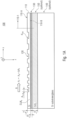
- Fig. 1A shows a schematic cross-sectional view of bandpass transmission filter 100 having a center wavelength ⁇ 0 of transmission according to an embodiment.
- the grating structure 120 has changing grating pitch values ⁇ i for diffracting a radiation "R" propagating in the waveguide structure 110 having a wavelength ⁇ 1 which is lower than the center wavelength ⁇ 0 , with ⁇ 1 ⁇ ⁇ 0 , and for reflecting, e.g., by means of a Bragg reflection, a radiation R in the waveguide structure 110 having a further wavelength ⁇ 2 which is higher than the center wavelengths ⁇ 0 , with ⁇ 2 > ⁇ 0 .
- the grating structure 120 may be formed in a first main surface region (or front face) 110-A of the waveguide structure 110.
- the radiation absorbing structure 130 may be an integrated part of the waveguide structure 110 or is formed as a layer, e.g., a dielectric layer, arranged adjacent to the waveguide structure 110, for absorbing a radiation R guided by the waveguide structure 110 having a wavelength ⁇ 3 higher than the wavelength ⁇ 2 , with ⁇ 0 ⁇ ⁇ 2 ⁇ ⁇ 3 .
- the waveguide structure 110 is arranged on a substrate 140, e.g., a semiconductor substrate, such as a silicon substrate, or a glass substrate, as exemplarily shown in Fig. 1A .
- a substrate 140 e.g., a semiconductor substrate, such as a silicon substrate, or a glass substrate, as exemplarily shown in Fig. 1A .
- the change in grating pitch values ⁇ i depends on the index i according to at least one of a linear function, an exponential function, a polynomial function or a combination thereof.
- the grating structure 120 may be formed as a "chirped" grating structure having monotonically changing (e.g. increasing or decreasing) grating pitch values ⁇ i .
- Fig. 1B shows a schematic exemplary representation of the diffraction regime, the Bragg reflection regime and sub-wavelength regime. It is to be noted that the regimes are depicted in Fig. 1B for a constant periodicity of the grating structure 120 (top) and for a constant wavelength (bottom).
- the transmission band is formed in the transmission window between the diffraction and Bragg reflection regime.
- the bandpass transmission filter 100 comprises the waveguide structure 110 with the grating structure 120 with changing grating pitch values ⁇ i in the waveguide structure 110, e.g., a chirped grating structure, in order to widen the diffraction regime and the reflection regime, i.e., in order to broaden the stop band of the resulting bandpass transmission filter 100.
- the transmission window between the diffraction and Bragg reflection regime is narrowed, leading to a narrow transmission band.
- the bandpass transmission filter 100 combines three physical effects in the form of diffraction, Bragg reflection and absorption.
- Fig. 1C shows a schematic plot of a combination of different Bragg gratings for providing a narrow transmission window between the diffraction and Bragg reflection regime.
- the illustration shows how the narrow transmission band can be created with a chirped grating.
- three different Bragg gratings I, II, III are combined, in order to narrow down the transmission window between the diffraction and Bragg reflection regime.
- the combination of all three gratings yields the combined characteristics shown in course IV with a thermal emitter, for example.
- Fig. 1D shows a schematic cross-sectional view (parallel to the x-z-plane) of the grating structure 120 on top of a considered waveguide platform, i.e. the waveguide structure 110, for illustrating a diffraction of short wavelengths (left figure) and a reflection of long wavelengths (right figure) according to an embodiment.
- grating structure 120 having the changing grating pitch values ⁇ i is described in detail together with simulation plots showing different filter characteristics of the bandpass transmission filter 100 for specific implementations.
- the grating structure is based on a modulation of the refractive index, e.g., based on a periodical modulation, an aperiodic modulation and/or monotonically varying (increasing or decreasing) modulation of the refractive index n 110 .
- Such a modulation of the refractive index n 110 of the grating structure 120 can be achieved, for example, by modifying the optical material properties of the waveguide structure 110 or by modifying the geometry of the waveguide structure 110, e.g., by a modification of the height and/or the width of the waveguide structure 110, which also leads to a modification, e.g., a periodic or aperiodic modification, of the effective mode index of the propagating wave n eff(110) and the resulting grating characteristics of the grating structure 120 in the waveguide structure 110.
- a modification e.g., a periodic or aperiodic modification
- Fig. 1D depicts the wave vectors of a mode propagating in a waveguide 110 with a grating structure 120 on top, for small wavelengths (a) and for the Bragg-wavelength (b) of the radiation R. Small wavelengths are diffracted, while the specific wavelength, where the Bragg condition holds , is reflected. Longer wavelengths ( ⁇ 0 n eff ⁇ 2 ⁇ ) ideally just see an effect on their propagation constants, but are not diffracted or reflected at all from the grating.
- ⁇ 2 is the incoming angle
- ⁇ 1 m the diffracted angle for the order m
- ⁇ is the wavelength in the material
- ⁇ is the pitch of the grating.
- n i is assumed to be purely real. Therefore the different propagation velocities have to be accounted for by adding the refractive indices of the materials to Equation 1.
- SiO 2 is further dielectric layer 150
- Si 3 N 4 is dielectric layer 130
- the two effects described above are used to form a narrow transmission band.
- the Bragg reflection is a narrow band effect, i.e. a grating with a single pitch would only reflect a narrow band.
- the grating pitch is changed, e.g. continuously increased (chirped), which leads to a broadening of the reflection band, which can therefore be used to narrow the transmission window between the diffraction and Bragg reflection regime.
- Fig. 1A shows a schematic representation of the waveguide structure 110 with the chirped grating 120.
- the grating structure 110 can be realized on a silicon or on insulator (dielectric) platform.
- the changing grating pitch values ⁇ i depend on at least one of a linear function, an exponential function and a polynomial function, wherein the changing grating pitch values ⁇ i may comprise a combination of a basis pitch value " ⁇ 0 " and a variable pitch value ⁇ i , wherein the variable pitch value is linearly changing, exponentially changing and/or polynomially changing with "i".
- the grating structure 120 may be a chirped grating structure having monotonically changing, i.e. increasing or decreasing, grating pitch values ⁇ i .
- the center pitch ⁇ center is calculated using a rearranged form of the Bragg condition (5), where ⁇ 0 is the vacuum wavelength at which high transmission is desired (center wavelength ⁇ 0 ) and n eff the effective mode index.
- the pitch of the higher number periods is calculated based on the variable pitch value ⁇ i .
- the continuous grating period change ⁇ i can be discretized to a minimum of e.g. 1 nm for lines and spaces (depending on the design rules). This can raise the need to repeat each individual grating period for a few times, before increasing the pitch ⁇ i , in order to achieve a sufficient stop-characteristic.
- ⁇ i ⁇ 0 + A ⁇ i + B ⁇ i 2 + C ⁇ i 3
- the radiation absorbing structure 130 at least partially covers a bottom face of the waveguide structure 110 having the grating structure 120.
- the waveguide structure 110 is arranged on a substrate 140, wherein a dielectric layer 130, which forms the radiation absorbing structure 130, and a further dielectric layer 150 are arranged between the waveguide structure 110 and the substrate 140.
- the further dielectric layer 150 is formed between the dielectric layer 130 and the substrate 140.
- the further dielectric layer 150 is formed between the waveguide structure 110 and the substrate 140, wherein the further dielectric layer 150 has a material thickness for suppressing a coupling of the waveguide mode from the waveguide structure 110 into the substrate 140.
- the waveguide structure 110 comprises one of a (poly) silicon (Poly-Si), Si, Ge, AIN and As 2 Se 3 material.
- the substrate 140 may comprise at least one of Si and glass material.
- a Si0 2 layer 150 ( ⁇ 2 ⁇ m) may be deposited on a Si substrate 140 in order to suppress coupling of the waveguide mode into the substrate 140.
- a thin Si 3 N 4 (e.g. 140 nm) layer 130 is used as absorbing layer for long wavelengths.
- the waveguide 110 on top may be made of silicon with a height of e.g. 660 nm.
- Eventually the grating 120 is etched into the top of the silicon waveguide 110.
- Figure 1A shows a schematic representation of the described platform.
- the waveguide structure 110 may comprise a waveguide extension structure 110-1, wherein the radiation absorbing layer 130 at least partially covers a face of the waveguide extension structure 110-1 for reducing a sideband transmission of the bandpass transmission filter 100.
- the bandpass transmission filter 100 may be used in combination with a broadband thermal emitter for providing a narrowband radiation source, which can be employed for various applications, e.g. optical sensors.
- the bandpass transmission filter 100 provides a spectrally broad stop-band with a narrow transmission band.
- the combination of this bandpass transmission filter 100 with a broadband source leads to a narrow band radiation source.
- the bandpass transmission filter 100 can be fabricated with low costs. When using a waveguide platform, for some embodiments, the bandpass transmission filter 100 can be fabricated without additional processing steps, which means no extra efforts and costs. To be more specific, the fabrication of such a bandpass transmission filter 100 requires no extra fabrication steps when carried out as sidewall grating 120, or one extra litho/etching process when carried out on top of the waveguide 110. This gives the possibility to easily create a low cost narrow band radiation source using a thermal emitter and the described bandpass transmission filter 100.
- a possible application of the bandpass transmission filter 100 may be an optical IR sensor.
- the bandpass transmission filter 100 can be combined with a thermal emitter in order to create a narrow band radiation source.
- the filtered radiation which is present at the end of the bandpass transmission filter 100 can be coupled into different kinds of waveguides (e.g. slab, strip, photonic crystals, etc.) which may act as sensor elements.
- the bandpass transmission filter 100 comprises a waveguide 110 with a changing or chirped grating 120, which is a grating 120 with a variable grating constant. Tailoring this grating and the interaction with the used materials allows creating a narrow transmission band, adapted to the desired wavelength.
- the bandpass transmission filter 100 provides a filter concept, which is well suited for optical integrated waveguides.
- the modulation is most favorably introduced by geometrical variations of the waveguide dimensions and the waveguide design can be tuned to the material characteristics.
- a changing or chirped grating 120 is engineered in order to create the transmission band filter 100, which can be used e.g. to create narrow-band IR sources.
- the transmission band filter 100 can be used e.g. to create narrow-band IR sources.
- three physical effects are combined, diffraction, Bragg reflection and absorption, wherein a tailored waveguide structure 110 allows realizing the narrow-band transmission filter 100 with a wide spectral rejection range.
- the filter 100 can be adapted for various application and fabrication tolerances.
- This narrow-band transmission filter 100 can be implemented to most waveguide designs, without significant additional fabrication costs.
- Bragg gratings, and also chirped Bragg gratings may be applied for an effective limitation of a very broad spectral rejection band.
- a waveguide design and a Bragg-grating design are combined.
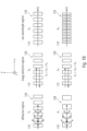
- Fig. 2A shows a schematic 3D top view of different schematic representation of changing or chirped gratings 120 on slab and strip waveguides 110 as different design options according to an embodiment.
- the waveguide structure 110 may be implemented as a slab waveguide having a top face grating 120.
- the waveguide structure 110 may comprises a strip waveguide having a top face grating 120.
- the waveguide structure 110 may comprise a strip waveguide having a side face grating 120.
- the waveguide structure may comprise a strip waveguide having a side face grating or having a top face grating (not shown in Fig. 2A ).
- the waveguide structure may comprise a slot waveguide having a side face grating or having a top face grating (not shown in Fig. 2A ).
- the waveguide structure may comprise a rib waveguide having a side face grating or having a top face grating (not shown in Fig. 2A ).
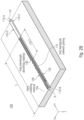
- Fig. 2B shows a schematic 3D top view of the bandpass transmission filter 100 with a strip waveguide 110 having the changing or "chirped" grating structure 120 integrated in the sidewalls 110-C, 110-D of the strip waveguide 110 and an absorbing layer for wavelengths > ⁇ 3 on top of the waveguide.
- the waveguide structure 110 comprises the waveguide extension structure 110-1, wherein the radiation absorbing layer 130 (at least partially) covers the first main surface region or top face 110-A in Fig. 2B of the waveguide extension structure 110-1 for reducing a sideband transmission of the filter 100.
- the long wavelength absorber 130 is placed on top of the waveguide structure 110, which may facilitate the fabrication process.
- Fig. 2B shows the bandpass transmission filter 100 using a strip waveguide 110, which can be used in order to filter a broadband source, e.g. thermal emitter (not shown in Fig. 2B ).
- the grating structure 120 is realized on the sidewalls 110-C, 110-D of the waveguide structure 110.
- the grating period ⁇ i for the depicted embodiment, it is also possible to arbitrarily vary the depth d 120 of the grating structure 120 in order to optimize the filter performance.
- the dielectric layer 130 of a long wavelength absorbing material is attached on the top (first main surface region) 110-A of the waveguide structure 110.
- the length L of this layer can be designed in order to sufficiently suppress the side band transmission at long wavelengths A 3 .
- the waveguide structure 110 is continued without the absorbing layer 130 on top in order to reduce the intrinsic losses.
- the center pitch ⁇ Center was 753 nm (calculated using Equation 5), the Gap ( ⁇ Gap ) was 18 nm and the variation ⁇ i was 2 nm. This leads to a variation of 1 nm for lines and spaces.
- the height h 110 of the waveguide was 660 nm and the depth d 120 of the grating was 100 nm.
- the thickness t 150 of the dielectric layer 130 e.g.
- the waveguide structure 110 was elongated (with the waveguide extension structure 110-1) for 5 pm, leading to a total filter length of 437.2 ⁇ m.
- FEM finite element method
- FEM finite element method
- FEM finite element method
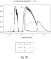
- Figs. 3A-C show FEM simulation results with (a) and without (b) taking into account material absorption, depicting the transmittance and the reflectance as well as the sum of both. Furthermore Fig. 3C shows a comparison of the transmittance through the grating filter with and without material absorption, and the transmittance through a plain slab waveguide with a length of 1.5 mm and taking into account the material absorption.
- the waveguide without grating transmits up to 9.5 ⁇ m before strong damping is induced due to leaking of the mode.
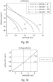
- Fig. 3D-E show schematic plots of the "diffraction angles" as a function of the wavelength, the grating pitch and the cladding material, and of the "grating pitch", which satisfies the condition for Bragg reflection as a function of the wavelength.
- Fig. 3D depicts the diffraction angles calculated according to Equation 4 for the minimum and maximum pitch ⁇ i , for the two dominant cladding materials in the form of the environmental atmosphere, e.g. air, and the further dielectric layer 150, i.e. the SiO 2 layer.
- the diffraction into the further dielectric layer 150, i.e. the SiO 2 layer already reaches the desired transmission wavelength ⁇ 0 , which is also visible in Fig. 3A , since the transmittance plus reflection R+T does not reach a value of 1.
- the stopband of the Bragg reflection there are very limited periods with a high pitch, only a small fraction of the radiation R with a wavelength around 4.26 ⁇ m is diffracted. Nevertheless, this effect leads to limitations for the stopband of the Bragg reflection.
- Fig. 3E shows the grating pitch which satisfies the condition for Bragg reflection as a function of the wavelength.
- the dashed lines mark the range for which Bragg condition is fulfilled with the used grating pitches ( ⁇ 4.32 ⁇ m to 5.28 ⁇ m).
- the Bragg condition is only satisfied up to 5.28 ⁇ m the grating influences the transmission up to ⁇ 5.53 ⁇ m.
- Fig. 3F-G show schematic plots of the filtered spectra of the bandpass transmission filter according to an embodiment.
- Fig. 3F shows the filtered spectra when the length of the waveguide structure 110, on which the chirped grating structure 120 is placed, is extended by 1.5 mm.
- the result shows that the side-band transmission can be reduced by increasing the length of the waveguide structure 110, e.g. by means of the waveguide extension structure 110-1, as the waveguide structure 110 has high losses for long wavelengths due to the used materials.
- the changing or chirped grating structure may be accordingly redesigned on the basis of the above equations.
- the interaction between waveguide 110 characteristics and material properties may be considered in order to achieve the bandpass transmission filter performance.
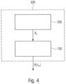
- Fig. 4 shows an exemplary block diagram of a narrowband radiation source 300 having the bandpass transmission filter 100 and a broadband radiation source 200, e.g. a thermal emitter, according to an embodiment.
- the narrowband radiation source 300 comprises the bandpass transmission filter 100 as described in Figs. 1A-B , 2A-B and 3A-G above.
- the narrowband radiation source 300 further comprises a broadband radiation source 200, e.g. a thermal emitter.
- the bandpass transmission filter 100 is arranged in a radiation R emission direction of the broadband radiation source 200 downstream to the broadband radiation source 200.
- the IR emitter may comprise a conductive strip, e.g. a semiconductor strip or a highly doped polysilicon material, having a main emission surface region vertical to the bandpass transmission filter 100 for emitting a broadband IR radiation R 0 in a main radiation emission direction to the bandpass transmission filter 100.
- the IR emitter may comprise a metallic cover layer which at least partially covers the main emission surface region of the conductive strip.
- the IR emitter may form a black body radiator and is configured to have in an actuated condition an operating temperature in a range between 600 and 1000 K, and wherein the IR emitter is connected to a power source for providing the electrical energy to bring the IR emitter in the actuated condition.
- the bandpass transmission filter 100 is arranged in an illumination direction downstream of the broadband radiation source 200 and is configured to filter the broadband IR radiation R 0 emitted by the IR emitter and to provide a filtered or narrowband IR radiation R( ⁇ 0 ) having a center wavelength ⁇ 0 .
Landscapes
- Physics & Mathematics (AREA)
- General Physics & Mathematics (AREA)
- Optics & Photonics (AREA)
- Engineering & Computer Science (AREA)
- Microelectronics & Electronic Packaging (AREA)
- Optical Integrated Circuits (AREA)
- Health & Medical Sciences (AREA)
- Toxicology (AREA)
Claims (13)
- Bandpassübertragungsfilter (100) mit einer Übertragungs-Mittenwellenlänge λ0, das folgende Merkmale aufweist:eine Wellenleiterstruktur (110), die auf einem Substrat (140) angeordnet ist,eine Gitterstruktur (120) in der Wellenleiterstruktur (110) mit einem Seitenflächengitter oder einem Oberseitenflächengitter, wobei die Gitterstruktur (120) sich ändernde Gitterabstandswerte Λi zum Ausbeugen einer geführten Strahlung in der Wellenleiterstruktur (110) mit Wellenlängen λ1, die kleiner als die Mittenwellenlänge λ0 sind, und zum Zurückreflektieren einer geführten Strahlung in der Wellenleiterstruktur mit einer Wellenlänge λ2, die größer als die Mittenwellenlänge λ0 ist, aufweist, undeine strahlungsabsorbierende Struktur (130), die als eine dielektrische Schicht ausgebildet ist, die benachbart zu der Wellenleiterstruktur (110) angeordnet ist, zum Absorbieren einer Strahlung, die durch die Wellenleiterstruktur (110) geführt wird, die eine Wellenlänge λ3 aufweist, die höher als die Wellenlänge λ2 ist, wobei λ0 < λ2 < λ3 gilt, wobei die strahlungsabsorbierende Struktur (130) eine Bodenfläche der Wellenleiterstruktur (110) mit der Gitterstruktur (120) zumindest teilweise bedeckt, und wobei eine weitere dielektrische Schicht (150) zwischen der Wellenleiterstruktur (110) und dem Substrat (140) gebildet ist, wobei die dielektrische Schicht (130) und die weitere dielektrische Schicht (150) zwischen der Wellenleiterstruktur (110) und dem Substrat (140) angeordnet sind, wobei die weitere dielektrische Schicht (150) zwischen der dielektrischen Schicht (130) und dem Substrat (140) gebildet ist, und wobei die weitere dielektrische Schicht (150) eine Materialdicke zum Unterdrücken einer Kopplung der Wellenleitermode von der Wellenleiterstruktur (110) in das Substrat (140) aufweist;wobei die Wellenleiterstruktur (110) ein Silizium-, Polysilizium-, Si-, Ge-, AIN- oder As2Se3-Material aufweist, wobei die dielektrische Schicht (130) ein Si3N4-Material aufweist, und wobei die weitere dielektrische Schicht (150) ein SiO2-Material aufweist.
- Bandpassübertragungsfilter (100) gemäß Anspruch 1, bei dem die sich ändernden Gitterabstandswerte Λi von mindestens einer von einer linearen Funktion, einer Exponentialfunktion und einer Polynomfunktion abhängen.
- Bandpassübertragungsfilter (100) gemäß Anspruch 1 oder 2, bei dem die sich ändernden Gitterabstandswerte Λi eine Kombination aus einem Basisabstandswert (Λ 0) und einem variablen Abstandswert (ΔΛi) aufweisen, wobei der variable Abstandswert sich linear ändert, sich exponentiell ändert und/oder sich polynomisch ändert.
- Bandpassübertragungsfilter (100) gemäß einem der vorhergehenden Ansprüche, bei dem die Gitterstruktur (120) eine gechirpte Gitterstruktur mit sich monoton ändernden Gitterabstandswerten Λi ist.
- Bandpassübertragungsfilter (100) gemäß einem der vorhergehenden Ansprüche, bei dem die Wellenleiterstruktur (110) einen Streifenwellenleiter mit einem Seitenflächengitter oder mit einem Oberseitenflächengitter (120) aufweist.
- Bandpassübertragungsfilter (100) gemäß einem der vorhergehenden Ansprüche, bei dem die Wellenleiterstruktur (110) einen Schlitzwellenleiter mit einem Seitenflächengitter oder mit einem Oberseitenflächengitter (120) aufweist.
- Bandpassübertragungsfilter (100) gemäß einem der vorhergehenden Ansprüche, bei dem die Wellenleiterstruktur (110) einen Rippenwellenleiter mit einem Seitenflächengitter oder mit einem Oberseitenflächengitter (120) aufweist.
- Bandpassübertragungsfilter (100) gemäß einem der Ansprüche 1 bis 5, bei dem die Wellenleiterstruktur (110) ein Plattenwellenleiter mit einem Oberseitenflächengitter (120) ist.
- Bandpassübertragungsfilter (100) gemäß einem der vorhergehenden Ansprüche, bei dem die Wellenleiterstruktur (110) eine Wellenleitererweiterungsstruktur (110-1) aufweist, ohne dass eine weitere Gitterstruktur (120) darauf angeordnet ist, wobei die strahlungsabsorbierende Struktur (130) zumindest teilweise eine Oberseitenfläche der Wellenleitererweiterungsstruktur (110-1) bedeckt, um eine Seitenbandtransmission des Filters (100) zu reduzieren.
- Bandpassübertragungsfilter (100) gemäß einem der vorhergehenden Ansprüche, bei dem die sich ändernden Gitterabstandswerte Λi abhängen von:- einer linearen Funktion mit Λi = Λ0, + ΔΛ × i , wobei "Λ0 " der Basisabstandswert ist und "ΔΛ × i" der variable Abstandswert ist, oder- einer linearen Funktion mit Λi = Λ0, + ΔΛ × (N - i) , wobei "Λ 0" der Basisabstandswert ist und "ΔΛ × (N - i)" der variable Abstandswert ist, oder- einer Exponentialfunktion mit Λi = Λ 0 + (F 1) i , wobei "Λ 0" der Basisabstandswert ist und (F 1) i der variable Abstandswert ist, oder- einer Exponentialfunktion mit Λi = Λ 0 × (F 2) i , wobei "Λ 0" der Basisabstandswert ist und (F 2) i der variable Abstandswert ist, oder- einer Polynomfunktion mit


- Bandpassübertragungsfilter (100) gemäß Anspruch 10, bei dem der Basisabstandswert "Λ 0" einen Mittenabstandswert "ΛCenter" und einen zusätzlichen Lückenwert "ΛGap" aufweist, und bei dem der Term "ΛCenter" abhängt von der Funktion:

- Bandpassübertragungsfilter (100) gemäß einem der vorhergehenden Ansprüche, bei dem der i-te Gitterabstandswert Λi N-mal mit N ≥ 4 wiederholt wird.
- Schmalband-Strahlungsquelle (300), die folgende Merkmale aufweist:das Bandpassübertragungsfilter (100) gemäß einem der vorhergehenden Ansprüche undeine Breitband-Strahlungsquelle (200),wobei das Bandpassübertragungsfilter (100) in einer Richtung einer Strahlungsemission (R) der Breitband-Strahlungsquelle (200) der Breitband-Strahlungsquelle (200) nachgelagert angeordnet ist.
Priority Applications (2)
| Application Number | Priority Date | Filing Date | Title |
|---|---|---|---|
| EP19161714.1A EP3705918B1 (de) | 2019-03-08 | 2019-03-08 | Bandpassübertragungsfilter und schmalbandstrahlungsquelle |
| US16/810,442 US11320586B2 (en) | 2019-03-08 | 2020-03-05 | Bandpass transmission filter and narrowband radiation source |
Applications Claiming Priority (1)
| Application Number | Priority Date | Filing Date | Title |
|---|---|---|---|
| EP19161714.1A EP3705918B1 (de) | 2019-03-08 | 2019-03-08 | Bandpassübertragungsfilter und schmalbandstrahlungsquelle |
Publications (2)
| Publication Number | Publication Date |
|---|---|
| EP3705918A1 EP3705918A1 (de) | 2020-09-09 |
| EP3705918B1 true EP3705918B1 (de) | 2025-04-30 |
Family
ID=65763273
Family Applications (1)
| Application Number | Title | Priority Date | Filing Date |
|---|---|---|---|
| EP19161714.1A Active EP3705918B1 (de) | 2019-03-08 | 2019-03-08 | Bandpassübertragungsfilter und schmalbandstrahlungsquelle |
Country Status (2)
| Country | Link |
|---|---|
| US (1) | US11320586B2 (de) |
| EP (1) | EP3705918B1 (de) |
Families Citing this family (5)
| Publication number | Priority date | Publication date | Assignee | Title |
|---|---|---|---|---|
| US12072534B2 (en) | 2021-08-27 | 2024-08-27 | Taiwan Semiconductor Manufacturing Company, Ltd. | Fiber to chip coupler and method of using |
| CN114859467B (zh) * | 2022-04-11 | 2023-02-17 | 上海交通大学 | 基于反向二元闪耀光栅的滤波器及制造方法 |
| US12449599B2 (en) * | 2023-01-13 | 2025-10-21 | Globalfoundries U.S. Inc. | Directional couplers with heterogenous claddings |
| CN116544781B (zh) * | 2023-04-13 | 2026-04-17 | 中国科学院半导体研究所 | 一种半导体锁模激光器及其制备方法 |
| CN120981746A (zh) * | 2023-07-05 | 2025-11-18 | 应用材料公司 | 作为用于增强现实波导组合器的抗反射涂层的图案化薄膜 |
Family Cites Families (6)
| Publication number | Priority date | Publication date | Assignee | Title |
|---|---|---|---|---|
| US3814498A (en) * | 1972-05-04 | 1974-06-04 | Bell Telephone Labor Inc | Integrated optical circuit devices employing optical gratings |
| JP3346440B2 (ja) * | 1994-09-30 | 2002-11-18 | 日本電信電話株式会社 | 透過型ファイバグレーティングフィルタの製造方法 |
| US5949934A (en) * | 1996-04-05 | 1999-09-07 | Fujikura, Ltd. | Optical waveguide grating and production method therefor |
| JPH09311238A (ja) * | 1996-05-22 | 1997-12-02 | Sumitomo Electric Ind Ltd | 光導波路型回折格子の作成方法 |
| JP2002189134A (ja) * | 2000-10-12 | 2002-07-05 | Matsushita Electric Ind Co Ltd | 光波長フィルタ及びその製造方法 |
| JP6089077B1 (ja) * | 2015-08-25 | 2017-03-01 | 沖電気工業株式会社 | 導波路型光回折格子及び光波長フィルタ |
-
2019
- 2019-03-08 EP EP19161714.1A patent/EP3705918B1/de active Active
-
2020
- 2020-03-05 US US16/810,442 patent/US11320586B2/en active Active
Non-Patent Citations (1)
| Title |
|---|
| WANG JUNJIA ET AL: "Integrated bandpass transmission filters based on Sagnac loops incorporating Bragg gratings in SOI", 2015 IEEE 12TH INTERNATIONAL CONFERENCE ON GROUP IV PHOTONICS (GFP), IEEE, 26 August 2015 (2015-08-26), pages 45 - 46, XP032798041, DOI: 10.1109/GROUP4.2015.7305976 * |
Also Published As
| Publication number | Publication date |
|---|---|
| US20200284956A1 (en) | 2020-09-10 |
| EP3705918A1 (de) | 2020-09-09 |
| US11320586B2 (en) | 2022-05-03 |
Similar Documents
| Publication | Publication Date | Title |
|---|---|---|
| EP3705918B1 (de) | Bandpassübertragungsfilter und schmalbandstrahlungsquelle | |
| Schulz et al. | Dispersion engineered slow light in photonic crystals: a comparison | |
| US6823111B2 (en) | Optical waveguide filters | |
| CN1279770A (zh) | 光波导窄带带阻滤波器 | |
| US9588339B2 (en) | Device for controlling the phase of an optical wavefront having juxtaposed metal-multidielectric-metal structures to induce a local shift | |
| JPWO2009087825A1 (ja) | フォトニック結晶体 | |
| Khonina et al. | Spectral characteristics of broad band-rejection filter based on Bragg grating, one-dimensional photonic crystal, and subwavelength grating waveguide | |
| KR20010068798A (ko) | 다중 클래딩 구조를 이용하여 온도 보상된 장주기 광섬유격자 필터 | |
| JP2005208331A (ja) | 分光光学素子 | |
| CN1292884A (zh) | 可调光纤布喇格和长周期光栅 | |
| US20040223693A1 (en) | Multidimensional optical gratings | |
| KR102074172B1 (ko) | 원형 공진기, 이를 포함하는 광 변환기 및 광학 소자 | |
| US6549707B1 (en) | Grating-type optical filter with apodised spectral response | |
| Fesenko et al. | Dispersion properties of Kolakoski-cladding hollow-core nanophotonic Bragg waveguide | |
| US20090067785A1 (en) | Optical device comprising an apodized bragg grating and method to apodize a bragg grating | |
| KR102568788B1 (ko) | 브래그 격자 및 이를 포함하는 분광 소자 | |
| Ranacher et al. | Design of a mid-infrared bandpass filter with large rejection bandwidth for silicon photonics | |
| CN113138432A (zh) | 一种基于石墨烯对的光子晶体 | |
| US6483955B2 (en) | Diffraction grating device | |
| JP2004505309A (ja) | 光学導波管フィルタ | |
| CN214174672U (zh) | 一种基于平面光波导的光栅滤波光器件 | |
| JP2000275442A (ja) | 光バンドパスフィルタ | |
| KR20090093798A (ko) | 플라즈모닉 광 도파로 | |
| JP4269056B2 (ja) | 高密度光くし型フィルタ及びその作製方法 | |
| Vardhan et al. | Design and analysis of a silicon 1-D photonic crystal waveguide for wide band reject filtering and DNA sensing |
Legal Events
| Date | Code | Title | Description |
|---|---|---|---|
| PUAI | Public reference made under article 153(3) epc to a published international application that has entered the european phase |
Free format text: ORIGINAL CODE: 0009012 |
|
| STAA | Information on the status of an ep patent application or granted ep patent |
Free format text: STATUS: THE APPLICATION HAS BEEN PUBLISHED |
|
| AK | Designated contracting states |
Kind code of ref document: A1 Designated state(s): AL AT BE BG CH CY CZ DE DK EE ES FI FR GB GR HR HU IE IS IT LI LT LU LV MC MK MT NL NO PL PT RO RS SE SI SK SM TR |
|
| AX | Request for extension of the european patent |
Extension state: BA ME |
|
| STAA | Information on the status of an ep patent application or granted ep patent |
Free format text: STATUS: REQUEST FOR EXAMINATION WAS MADE |
|
| 17P | Request for examination filed |
Effective date: 20201022 |
|
| RBV | Designated contracting states (corrected) |
Designated state(s): AL AT BE BG CH CY CZ DE DK EE ES FI FR GB GR HR HU IE IS IT LI LT LU LV MC MK MT NL NO PL PT RO RS SE SI SK SM TR |
|
| STAA | Information on the status of an ep patent application or granted ep patent |
Free format text: STATUS: EXAMINATION IS IN PROGRESS |
|
| 17Q | First examination report despatched |
Effective date: 20210319 |
|
| GRAP | Despatch of communication of intention to grant a patent |
Free format text: ORIGINAL CODE: EPIDOSNIGR1 |
|
| STAA | Information on the status of an ep patent application or granted ep patent |
Free format text: STATUS: GRANT OF PATENT IS INTENDED |
|
| RIC1 | Information provided on ipc code assigned before grant |
Ipc: G02B 6/02 20060101ALN20241024BHEP Ipc: G02B 6/293 20060101ALI20241024BHEP Ipc: G02B 6/42 20060101ALI20241024BHEP Ipc: G02B 6/124 20060101ALI20241024BHEP Ipc: G02B 6/12 20060101AFI20241024BHEP |
|
| INTG | Intention to grant announced |
Effective date: 20241114 |
|
| P01 | Opt-out of the competence of the unified patent court (upc) registered |
Free format text: CASE NUMBER: APP_1161/2025 Effective date: 20250108 |
|
| GRAS | Grant fee paid |
Free format text: ORIGINAL CODE: EPIDOSNIGR3 |
|
| GRAA | (expected) grant |
Free format text: ORIGINAL CODE: 0009210 |
|
| STAA | Information on the status of an ep patent application or granted ep patent |
Free format text: STATUS: THE PATENT HAS BEEN GRANTED |
|
| AK | Designated contracting states |
Kind code of ref document: B1 Designated state(s): AL AT BE BG CH CY CZ DE DK EE ES FI FR GB GR HR HU IE IS IT LI LT LU LV MC MK MT NL NO PL PT RO RS SE SI SK SM TR |
|
| REG | Reference to a national code |
Ref country code: CH Ref legal event code: EP Ref country code: GB Ref legal event code: FG4D |
|
| REG | Reference to a national code |
Ref country code: DE Ref legal event code: R096 Ref document number: 602019069238 Country of ref document: DE |
|
| REG | Reference to a national code |
Ref country code: IE Ref legal event code: FG4D |
|
| REG | Reference to a national code |
Ref country code: NL Ref legal event code: MP Effective date: 20250430 |
|
| REG | Reference to a national code |
Ref country code: AT Ref legal event code: MK05 Ref document number: 1790519 Country of ref document: AT Kind code of ref document: T Effective date: 20250430 |
|
| PG25 | Lapsed in a contracting state [announced via postgrant information from national office to epo] |
Ref country code: ES Free format text: LAPSE BECAUSE OF FAILURE TO SUBMIT A TRANSLATION OF THE DESCRIPTION OR TO PAY THE FEE WITHIN THE PRESCRIBED TIME-LIMIT Effective date: 20250430 Ref country code: PT Free format text: LAPSE BECAUSE OF FAILURE TO SUBMIT A TRANSLATION OF THE DESCRIPTION OR TO PAY THE FEE WITHIN THE PRESCRIBED TIME-LIMIT Effective date: 20250901 Ref country code: FI Free format text: LAPSE BECAUSE OF FAILURE TO SUBMIT A TRANSLATION OF THE DESCRIPTION OR TO PAY THE FEE WITHIN THE PRESCRIBED TIME-LIMIT Effective date: 20250430 |
|
| REG | Reference to a national code |
Ref country code: LT Ref legal event code: MG9D |
|
| PG25 | Lapsed in a contracting state [announced via postgrant information from national office to epo] |
Ref country code: NO Free format text: LAPSE BECAUSE OF FAILURE TO SUBMIT A TRANSLATION OF THE DESCRIPTION OR TO PAY THE FEE WITHIN THE PRESCRIBED TIME-LIMIT Effective date: 20250730 Ref country code: GR Free format text: LAPSE BECAUSE OF FAILURE TO SUBMIT A TRANSLATION OF THE DESCRIPTION OR TO PAY THE FEE WITHIN THE PRESCRIBED TIME-LIMIT Effective date: 20250731 |
|
| PG25 | Lapsed in a contracting state [announced via postgrant information from national office to epo] |
Ref country code: PL Free format text: LAPSE BECAUSE OF FAILURE TO SUBMIT A TRANSLATION OF THE DESCRIPTION OR TO PAY THE FEE WITHIN THE PRESCRIBED TIME-LIMIT Effective date: 20250430 Ref country code: NL Free format text: LAPSE BECAUSE OF FAILURE TO SUBMIT A TRANSLATION OF THE DESCRIPTION OR TO PAY THE FEE WITHIN THE PRESCRIBED TIME-LIMIT Effective date: 20250430 |
|
| PG25 | Lapsed in a contracting state [announced via postgrant information from national office to epo] |
Ref country code: BG Free format text: LAPSE BECAUSE OF FAILURE TO SUBMIT A TRANSLATION OF THE DESCRIPTION OR TO PAY THE FEE WITHIN THE PRESCRIBED TIME-LIMIT Effective date: 20250430 |
|
| PG25 | Lapsed in a contracting state [announced via postgrant information from national office to epo] |
Ref country code: HR Free format text: LAPSE BECAUSE OF FAILURE TO SUBMIT A TRANSLATION OF THE DESCRIPTION OR TO PAY THE FEE WITHIN THE PRESCRIBED TIME-LIMIT Effective date: 20250430 |
|
| PG25 | Lapsed in a contracting state [announced via postgrant information from national office to epo] |
Ref country code: AT Free format text: LAPSE BECAUSE OF FAILURE TO SUBMIT A TRANSLATION OF THE DESCRIPTION OR TO PAY THE FEE WITHIN THE PRESCRIBED TIME-LIMIT Effective date: 20250430 |
|
| PG25 | Lapsed in a contracting state [announced via postgrant information from national office to epo] |
Ref country code: RS Free format text: LAPSE BECAUSE OF FAILURE TO SUBMIT A TRANSLATION OF THE DESCRIPTION OR TO PAY THE FEE WITHIN THE PRESCRIBED TIME-LIMIT Effective date: 20250731 |
|
| PG25 | Lapsed in a contracting state [announced via postgrant information from national office to epo] |
Ref country code: IS Free format text: LAPSE BECAUSE OF FAILURE TO SUBMIT A TRANSLATION OF THE DESCRIPTION OR TO PAY THE FEE WITHIN THE PRESCRIBED TIME-LIMIT Effective date: 20250830 |
|
| PG25 | Lapsed in a contracting state [announced via postgrant information from national office to epo] |
Ref country code: LV Free format text: LAPSE BECAUSE OF FAILURE TO SUBMIT A TRANSLATION OF THE DESCRIPTION OR TO PAY THE FEE WITHIN THE PRESCRIBED TIME-LIMIT Effective date: 20250430 |
|
| PG25 | Lapsed in a contracting state [announced via postgrant information from national office to epo] |
Ref country code: DK Free format text: LAPSE BECAUSE OF FAILURE TO SUBMIT A TRANSLATION OF THE DESCRIPTION OR TO PAY THE FEE WITHIN THE PRESCRIBED TIME-LIMIT Effective date: 20250430 Ref country code: SM Free format text: LAPSE BECAUSE OF FAILURE TO SUBMIT A TRANSLATION OF THE DESCRIPTION OR TO PAY THE FEE WITHIN THE PRESCRIBED TIME-LIMIT Effective date: 20250430 |
|
| PG25 | Lapsed in a contracting state [announced via postgrant information from national office to epo] |
Ref country code: CZ Free format text: LAPSE BECAUSE OF FAILURE TO SUBMIT A TRANSLATION OF THE DESCRIPTION OR TO PAY THE FEE WITHIN THE PRESCRIBED TIME-LIMIT Effective date: 20250430 |
|
| PG25 | Lapsed in a contracting state [announced via postgrant information from national office to epo] |
Ref country code: EE Free format text: LAPSE BECAUSE OF FAILURE TO SUBMIT A TRANSLATION OF THE DESCRIPTION OR TO PAY THE FEE WITHIN THE PRESCRIBED TIME-LIMIT Effective date: 20250430 |
|
| PG25 | Lapsed in a contracting state [announced via postgrant information from national office to epo] |
Ref country code: SK Free format text: LAPSE BECAUSE OF FAILURE TO SUBMIT A TRANSLATION OF THE DESCRIPTION OR TO PAY THE FEE WITHIN THE PRESCRIBED TIME-LIMIT Effective date: 20250430 Ref country code: RO Free format text: LAPSE BECAUSE OF FAILURE TO SUBMIT A TRANSLATION OF THE DESCRIPTION OR TO PAY THE FEE WITHIN THE PRESCRIBED TIME-LIMIT Effective date: 20250430 |
|
| PG25 | Lapsed in a contracting state [announced via postgrant information from national office to epo] |
Ref country code: IT Free format text: LAPSE BECAUSE OF FAILURE TO SUBMIT A TRANSLATION OF THE DESCRIPTION OR TO PAY THE FEE WITHIN THE PRESCRIBED TIME-LIMIT Effective date: 20250430 |
|
| REG | Reference to a national code |
Ref country code: DE Ref legal event code: R097 Ref document number: 602019069238 Country of ref document: DE |
|
| PLBE | No opposition filed within time limit |
Free format text: ORIGINAL CODE: 0009261 |
|
| STAA | Information on the status of an ep patent application or granted ep patent |
Free format text: STATUS: NO OPPOSITION FILED WITHIN TIME LIMIT |
|
| REG | Reference to a national code |
Ref country code: CH Ref legal event code: L10 Free format text: ST27 STATUS EVENT CODE: U-0-0-L10-L00 (AS PROVIDED BY THE NATIONAL OFFICE) Effective date: 20260311 |
|
| 26N | No opposition filed |
Effective date: 20260202 |