EP3704697B1 - Referenzspannungsgenerator für widerstandsspeicheranordnung - Google Patents
Referenzspannungsgenerator für widerstandsspeicheranordnung Download PDFInfo
- Publication number
- EP3704697B1 EP3704697B1 EP18872763.0A EP18872763A EP3704697B1 EP 3704697 B1 EP3704697 B1 EP 3704697B1 EP 18872763 A EP18872763 A EP 18872763A EP 3704697 B1 EP3704697 B1 EP 3704697B1
- Authority
- EP
- European Patent Office
- Prior art keywords
- bit line
- memory
- resistive
- voltage
- vref
- Prior art date
- Legal status (The legal status is an assumption and is not a legal conclusion. Google has not performed a legal analysis and makes no representation as to the accuracy of the status listed.)
- Active
Links
Images

Classifications
-
- G—PHYSICS
- G11—INFORMATION STORAGE
- G11C—STATIC STORES
- G11C5/00—Details of stores covered by group G11C11/00
- G11C5/14—Power supply arrangements, e.g. power down, chip selection or deselection, layout of wirings or power grids, or multiple supply levels
- G11C5/147—Voltage reference generators, voltage or current regulators; Internally lowered supply levels; Compensation for voltage drops
-
- G—PHYSICS
- G11—INFORMATION STORAGE
- G11C—STATIC STORES
- G11C11/00—Digital stores characterised by the use of particular electric or magnetic storage elements; Storage elements therefor
- G11C11/02—Digital stores characterised by the use of particular electric or magnetic storage elements; Storage elements therefor using magnetic elements
- G11C11/16—Digital stores characterised by the use of particular electric or magnetic storage elements; Storage elements therefor using magnetic elements using elements in which the storage effect is based on magnetic spin effect
- G11C11/161—Digital stores characterised by the use of particular electric or magnetic storage elements; Storage elements therefor using magnetic elements using elements in which the storage effect is based on magnetic spin effect details concerning the memory cell structure, e.g. the layers of the ferromagnetic memory cell
-
- G—PHYSICS
- G11—INFORMATION STORAGE
- G11C—STATIC STORES
- G11C11/00—Digital stores characterised by the use of particular electric or magnetic storage elements; Storage elements therefor
- G11C11/02—Digital stores characterised by the use of particular electric or magnetic storage elements; Storage elements therefor using magnetic elements
- G11C11/16—Digital stores characterised by the use of particular electric or magnetic storage elements; Storage elements therefor using magnetic elements using elements in which the storage effect is based on magnetic spin effect
- G11C11/165—Auxiliary circuits
- G11C11/1653—Address circuits or decoders
- G11C11/1655—Bit-line or column circuits
-
- G—PHYSICS
- G11—INFORMATION STORAGE
- G11C—STATIC STORES
- G11C11/00—Digital stores characterised by the use of particular electric or magnetic storage elements; Storage elements therefor
- G11C11/02—Digital stores characterised by the use of particular electric or magnetic storage elements; Storage elements therefor using magnetic elements
- G11C11/16—Digital stores characterised by the use of particular electric or magnetic storage elements; Storage elements therefor using magnetic elements using elements in which the storage effect is based on magnetic spin effect
- G11C11/165—Auxiliary circuits
- G11C11/1673—Reading or sensing circuits or methods
-
- G—PHYSICS
- G11—INFORMATION STORAGE
- G11C—STATIC STORES
- G11C13/00—Digital stores characterised by the use of storage elements not covered by groups G11C11/00, G11C23/00, or G11C25/00
- G11C13/0002—Digital stores characterised by the use of storage elements not covered by groups G11C11/00, G11C23/00, or G11C25/00 using resistive RAM [RRAM] elements
- G11C13/0021—Auxiliary circuits
- G11C13/0023—Address circuits or decoders
- G11C13/0026—Bit-line or column circuits
-
- G—PHYSICS
- G11—INFORMATION STORAGE
- G11C—STATIC STORES
- G11C13/00—Digital stores characterised by the use of storage elements not covered by groups G11C11/00, G11C23/00, or G11C25/00
- G11C13/0002—Digital stores characterised by the use of storage elements not covered by groups G11C11/00, G11C23/00, or G11C25/00 using resistive RAM [RRAM] elements
- G11C13/0021—Auxiliary circuits
- G11C13/004—Reading or sensing circuits or methods
- G11C2013/0054—Read is performed on a reference element, e.g. cell, and the reference sensed value is used to compare the sensed value of the selected cell
Definitions
- the disclosure herein relates generally to resistive memory arrays, and more specifically to a method and apparatus of generating a reference voltage for resistive memory arrays.
- MRAM Magnetic random access memory
- DRAM dynamic random access memory
- MRAM memory cells use resistive-based memory cells to represent stored data through different resistance values.
- resistance-based memory cells may exhibit a resistance that varies based on a stored logic state.
- Example resistance-based memory cells may include, but are not limited to, spin-transfer-torque, spin-orbit-torque, resistor random access memory (ReRAM), phase change RAM, and/or carbon nanotube memory cells.
- spin-torque-transfer memory relies on an equivalent resistance of a magnetic tunnel junction (MTJ) to provide non-volatile storage.
- MTJ magnetic tunnel junction
- the resistance-based memory cells may be programmed to different states (e.g., to represent a logic 0 or logic 1) by varying a current and/or a voltage driven through the memory cells during program (e.g., write) operations.
- program e.g., write
- the resistance of the resistance-based memory cells may be determined by passing a controlled current through the cells and comparing the resulting voltage to a reference voltage.
- the reference voltage for an MRAM array should not only be stable but should also enable the different states of the memory cells to be easily distinguished.
- Conventional approaches to reference voltage generation may not consider factors such as parasitic resistances and capacitances, local voltage fluctuations or bit line resistance-capacitance (RC) delays associated with MRAM arrays. These factors may cause uncertainty in the reference voltage and thereby cause erroneous data to be retrieved from the memory array. As such, it is desirable to have a voltage reference that may accommodate MRAM array implementations.
- ReRAM resistance-based random access memory
- RTB reference current circuit
- US 2009/0027953 discloses a phase change memory device which includes a plurality of word lines arranged in a row direction and a plurality of bit lines arranged in a column direction. A plurality of reference bit line and a plurality of clamp bit lines are arranged in the column direction.
- a cell array block including a phase change resistance cell is arranged where a word line and a bit line intersect.
- a reference cell array block is formed where a word line and the reference bit line intersect.
- the reference cell array block is configured to output a reference current.
- a clamp cell array block is formed where a word line and a clamp bit line intersect.
- the clamp cell array block is configured to output a clamp current.
- a sense amplifier is connected to each of the bit lines and is configured to receive a clamp voltage and a reference voltage.
- determining encompasses a wide variety of actions. For example, “determining” may include calculating, computing, processing, deriving, investigating, looking up (e.g., looking up in a table, a database or another data structure), ascertaining and the like. Also, “determining” may include receiving (e.g., receiving information), accessing (e.g., accessing data in a memory) and the like. Also, “determining” may include resolving, selecting, choosing, establishing and the like. Also, “determining” may include measuring, estimating, and the like.
- generating encompasses a wide variety of actions. For example, “generating” may include calculating, causing, computing, creating, determining, processing, deriving, investigating, making, producing, providing, giving rise to, leading to, resulting in, looking up (e.g., looking up in a table, a database or another data structure), ascertaining and the like. Also, “generating” may include receiving (e.g., receiving information), accessing (e.g., accessing data in a memory) and the like. Also, “generating” may include resolving, selecting, choosing, establishing and the like.
- a phrase referring to "at least one of" a list of items refers to any combination of those items, including single members.
- "at least one of: a, b, or c” is intended to cover a, b, c, a-b, a-c, b-c, and a-b-c, as well as any such list including multiples of the same members (e.g., any lists that include aa, bb, or cc).
- a single block may be described as performing a function or functions; however, in actual practice, the function or functions performed by that block may be performed in a single component or across multiple components, and/or may be performed using hardware, using software, or using a combination of hardware and software.
- various illustrative components, blocks, modules, circuits, and steps are described below generally in terms of their functionality. Whether such functionality is implemented as hardware or software depends upon the particular application and design constraints imposed on the overall system. Skilled artisans may implement the described functionality in varying ways for each particular application, but such implementation decisions should not be interpreted as causing a departure from the scope of the claims.
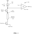
- FIG. 1 is a simplified schematic diagram 100 of an example resistance-based memory cell implementation.
- the schematic diagram 100 includes a resistive bit cell 110, a column current source I COL 120, a word line field effect transistor (FET) M1, a bit line FET M2, and a sense amp 130.
- FET word line field effect transistor
- the column current source I COL 120 may provide a bias current I BIAS for the resistive bit cell 110.
- the column current source I COL 120 may provide the bias current I BIAS for an entire column of resistive bit cells (not shown for simplicity).
- the resistive bit cell 110 may exhibit a varying resistance based on whether a logic 0 or a logic 1 is stored within the cell.
- Example implementations of the resistive bit cell 110 may include, but are not limited to, spin-transfer-torque, spin-orbit-torque, resistor random access memory (ReRAM), phase change RAM, and/or carbon nanotube memory cells.
- a voltage is generated at node N1 (e.g., a bit line associated with the resistive bit cell 110) based, at least in part, on the resistance of the resistive bit cell 110 and the bias current I BIAS .
- the sense amp 130 compares the voltage of the bit line through the bit line FET M2 to a reference voltage Vref and determines whether the voltage of the bit line (and therefore the resistive bit cell 110) is representative of a logic 0 or a logic 1.
- the source of the word line FET M1 may be coupled to any technically feasible voltage or node, shown here as "source line" for simplicity.
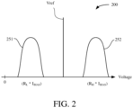
- FIG. 2 is a graph 200 depicting a relationship between voltages associated with a resistance from the resistive bit cell 110 of FIG. 1 and the reference voltage Vref in accordance with some implementations.
- the resistive bit cell 110 may be a "binary" bit cell and may have a first resistance when storing a first logic state and a second resistance when storing a second logic state.
- the resistive bit cell 110 may have a resistance of approximately 2000 ohms when storing a logic 0 and a resistance of approximately 4000 ohms when storing a logic 1.
- the resistive bit cell 110 may have a resistance of approximately 2000 ohms when storing a logic 1 and a resistance of approximately 4000 ohms when storing a logic 0.
- any suitable resistance may represent any logic state or states.
- the column current source I COL 120 may provide a bias current I BIAS to the resistive bit cell 110.
- a first resistance R L due to the resistive bit cell 110 may provide a first voltage distribution 251 (e.g., R L ⁇ I BIAS ) to represent a first logic state and a second resistance R H may provide a second voltage distribution 252 (e.g., R H ⁇ I BIAS ) to represent a second logic state.
- the voltage reference Vref may be selected so that the first voltage distribution 251 is easily distinguished from the second voltage distribution 252. In this manner, the stored logic states of the resistive bit cell 110 may easily be distinguished.
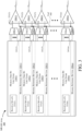
- FIG. 3 depicts a block diagram of an example implementation of a magnetic random access memory (MRAM) array 300.
- the MRAM array 300 may include a number of n memory data bit line groups 310(1)-310(n), n memory reference bit lines 320(1)-320(n), n memory data bit line multiplexers 330(1)-330(n), n reference bit line selectors 340(1)-340(n), and n sense amps 350(1)-350(n).
- Each memory data bit line group 310(1)-310(n) may include resistive bit cells 311(1)-311(n) (such as an implementation of the resistive bit cell 110 of FIG. 1 ) arranged in an array (array not shown for simplicity).
- each memory data bit line group 310(1)-310(n) may store a one bit vector (e.g. one data bit) for a plurality of words.
- a 32 bit word may include 32 memory data bit line groups that may be concatenated to form the 32 bit word.
- the memory data bit line multiplexers 330(1)-330(n) may select one of the memory data bit lines (e.g., one of the resistive bit cells in the resistive bit cells 311(1)-311(n)) in the memory data bit line group 310(1)-310(n). For example, during a read operation, a memory data bit line within the memory data bit line group 310(1)-310(n) may be activated by word line and bit line signals (e.g., as shown in FIG. 1 ). The selected memory data bit lines 331(1)-331(n) may be coupled from the memory data bit line multiplexers 330(1)-330(n) to the sense amps 350(1)-350(n).
- the selected memory data bit lines 331(1)-331(n) may carry a voltage from a selected resistive bit cell from the resistive bit cells 311(1)-311(n) of the memory data bit line group 310(1)-310(n).
- the memory data bit line multiplexers 330(1)-330(n) may be at least partially implemented with a bit line FET (such as FET M2 of FIG. 1 ).
- the sense amps 350(1)-350(n) may compare the voltage from the selected memory data bit lines 331(1)-331(n) with a reference voltage (Vref) 360.
- Vref reference voltage
- the sense amps 350(1)-350(n) may be an implementation of the sense amp 130 of FIG. 1 . If the voltage associated with the selected memory data bit lines 331(1)-331(n) is greater than the Vref 360, then the data bit stored by the associated resistance bit cell (e.g., in the selected resistive bit cells 311(1)-311(n)) may be interpreted by the sense amps 350(1)-350(n) to be a first logic state.
- each sense amp 350(1)-350(n) may generate one output data bit.
- the sense amps 350(1)-350(n) may generate a n-bit word (Dout(1)-Dout(n)).
- the number n may be 32. In some other implementations, the number n may be any feasible number.
- the memory reference bit lines 320(1)-320(n) may each generate a voltage that may be coupled together to generate the Vref 360.
- each memory reference bit line 320(1)-320(n) include at least one resistance-based memory cell (such as the resistance bit cell 110 of FIG. 1 ).
- the memory reference bit lines 320(1)-320(n) may each include a resistive bit cell similar to the resistive bit cells 311(1)-311(n) included in the memory data bit line groups 310(1)-310(n).
- the memory reference bit lines 320(1)-320(n) may be configured to generate one of two voltages: a first voltage based on the resistance R H or a second voltage based on the resistance R L .
- the reference bit line selectors 340(1)-340(n) may provide a voltage 341(1)-341(n) from each of the memory reference bit lines 320(1)-320(n) to the Vref 360. In this manner, the Vref 360 may be determined by logic states of the resistive bit cells within the memory reference bit lines 320(1)-320(n).
- the Vref 360 may be adjusted (trimmed) by the programming of the resistive bit cells included within the memory reference bit lines 320(1)-320(n). For example, increasing the number of resistive bit cells within the memory reference bit lines 320(1)-320(n) programmed to have the resistance R H and decreasing the number of resistive bit cells within the memory reference bit lines 320(1)-320(n) programmed to have the resistance R L may bias the Vref 360 toward the voltage associated with the resistance R H .
- the R H and R L resistances may be alternated (interleaved) within the memory reference bit lines 320(1)-320(n) and the associated reference bit line selectors 340(1)-340(n).
- the memory reference bit line 320(1) and the reference bit line selector 340(1) may provide a voltage associated with the resistance R H
- the memory reference bit line 320(2) and the reference bit line selector 340(2) may provide a voltage associated with the resistance R L
- the memory reference bit lines 320(3)-320(n) and the reference bit line selectors 340(3)-340(n) may alternate providing voltages associated with the resistances R H and R L .
- a memory reference bit line 320(1)-320(n) is disposed adjacent to a corresponding memory data bit line group 310(1)-310(n). More evenly distributed voltages associated with the R H and R L resistances across the area associated with the MRAM array 300 may enable the Vref 360 to more closely average out any voltage and/or parasitic fluctuations within the MRAM array 300.
- one half of the available memory reference bit lines 320(1)-320(n) may be configured to a first logic state and one half of the available memory reference bit lines 320(1)-320(n) may be configured to a second logic state.
- Such a configuration may provide a Vref 360 that may be an average (mean) of the voltage associated with the R H resistance and the voltage associated with the R L resistance.
- 32 memory reference bit lines 320(1)-320(n) may be used to cooperatively generate the Vref 360.
- the bit width of a data word, and therefore the number of memory reference bit lines 320(1)-320(n) may be any feasible number.
- the reference voltage Vref may be generated by the resistive bit cells of the memory reference bit lines 320(1)-320(n) connected in parallel though Vref 360.
- this connection achieves current-resistance (IR) averaging and/or resistance-capacitance (RC) averaging.
- IR current-resistance
- RC resistance-capacitance
- the Vref 360 may be based on similar resistive bit cell structures that may be used to implement resistive bit cells 311(1)-311(n). Therefore, the Vref 360 may advantageously track process variations, array parasitics, local voltage fluctuations, resistive-capacitive (RC) delays and other local and global aspects which may affect the operation of the MRAM array 300.
- RC resistive-capacitive
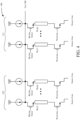
- FIG. 4 is a simplified schematic diagram 400 illustrating an example implementation of a plurality of the memory reference bit lines within the MRAM array 300 of FIG. 3 .
- each of the memory reference bit lines 320(1)-320(n) may generate a voltage associated with a resistance R H or a resistance R L
- a number n of memory reference bit lines 320(1)-320(n) may be used to generate the Vref 360.
- the schematic diagram 400 shows first group 410 including a number of p R H resistors and a second group 411 including a number q R L resistors.
- the Vref 360 may be trimmed by programming numbers of resistive bit cells included in the memory reference bit lines 320(1)-320(n) to have either a resistance R H or a resistance R L .
- programming more resistive bit cells to generate voltages associated with the resistance R H and fewer resistive bit cells to generate voltages associated with the resistance R L may bias the Vref 360 toward the voltage associated with the resistance R H .
- programming more resistive bit cells to generate voltages associated with the resistance R L and fewer resistive bit cells to generate voltages associated with the resistance R H may bias the Vref 360 toward the voltage associated with the resistance R L .
- the Vref 360 may be tuned (trimmed) to achieve near optimal performance.
- FIG. 5 is a graph 500 depicting another relationship between voltages associated with a resistance from the resistive bit cell 110 of FIG. 1 and the Vref 360.
- the resistive bit cell 110 may be a binary bit cell and may have a first resistance when storing the first logic state and a second resistance when storing the second logic state.
- the bias current I BIAS from current source I COL 120 of FIG. 1 may enable the generation of the first voltage distribution 251 and the second voltage distribution 252 of FIG. 2 .
- an initial Vref 510 may not be symmetric between the first voltage distribution 251 and the second voltage distribution 252.
- the initial Vref 510 may be based on an initial number of resistive bit cells configured to provide a resistance R H and a second number of resistive bit cells configured to provide a resistance R L .
- Vref may be adjusted through a tuning range 520 by changing the distribution of resistances R H and resistances R L (for example, within the memory reference bit lines 320(1)-320(n) of the MRAM array 300) contributing to the Vref.
- a fine-tuned Vref 530 may be adjusted to provide the Vref 360 (shown in FIG. 3 ).
- the first voltage distribution 251 and the second voltage distribution 252 may be characterized (measured) to determine an optimal voltage for Vref.
- Vref may be substantially midway between the first voltage distribution 251 and the second voltage distribution 252.
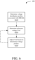
- FIG. 6 is a flowchart depicting an example operation 600 for providing a reference voltage of an MRAM array.
- the operation 600 may be performed by any feasible processor, computer system, state machine or other suitable device.
- the operation begins as the controller determines voltage distribution profiles associated with the MRAM array (610).
- the controller may characterize a plurality of resistive bit cells programmed into a first logic state and a second logic state to determine the associated voltage distribution profiles.
- the controller determines the reference voltage Vref (620).
- the controller may configure a first number of resistive bit cells associated with the memory reference bit lines 320(1)-320(n) of FIG. 3 to the first logic state and a second number of resistive bit cells of the memory reference bit lines 320(1)-320(n) of FIG. 3 to the second logic state and determine (e.g., measure) the reference voltage Vref.
- the controller adjusts the Vref based on the determined reference voltage Vref and the determined voltage distribution profiles associated with the MRAM (630).
- the controller may change the distribution of resistive bit cells configured to store the first logic state and the second logic state to change the value of the voltage Vref.
- the controller may optionally iterate the operation 600 by returning to 620 (optional iteration shown by dashed line in FIG. 6 ).
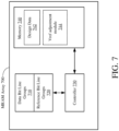
- FIG. 7 depicts an implementation of a MRAM array 700.
- the MRAM array 700 may be another implementation of the MRAM array 300 of FIG. 3 .
- the MRAM array 700 may include data bit line groups 710, reference bit line groups 720, a controller 730, and a memory 740.
- the controller 730 may be coupled to the data bit line groups 710 and the memory data bit line groups 720.
- the data bit line groups 710 may be an implementation of the memory data bit line groups 310(1)-310(n) of FIG. 3 .
- the memory data bit line groups 710 may include one or more resistive bit cells configured to store data (not shown for simplicity).
- the reference bit line groups 720 may be an implementation of the memory reference bit lines 320(1)-320(n) of FIG. 3 .
- the reference bit line groups 720 may be configured to provide one or more voltages that may, in turn, be used to provide a reference voltage Vref.
- the controller 730 which is also coupled to the memory 740, may be any one or more suitable controllers capable of executing scripts or instructions of one or more software programs stored within the MRAM array 700 (e.g., within the memory 740).
- the controller 730 and the memory 740 may be separate from the MRAM array 700.
- the controller 730 and the memory 740 may be in a chip or die separate from the data bit line groups 710 and/or the memory data bit line groups 720.
- the controller 730 may be a host processor and the memory 740 may be system memory associated with the host processor.
- the memory 740 may be a solid state, magnetic, optical, magneto-optical, or any other suitable device capable of transient and/or non-volatile storage.
- the memory 740 may store design data 742.
- the design data 742 may include design information associated with the MRAM array 700.
- the design data 742 may include information describing the number of resistive bit cells included within the reference bit line groups 720.
- memory 740 may also include a non-transitory computer-readable storage medium (e.g., one or more nonvolatile memory elements, such as EPROM, EEPROM, Flash memory, a hard drive, etc.) that may include a Vref adjustment module 744.
- the controller 730 may execute the Vref adjustment module 744 to generate and/or adjust the generation of a reference voltage Vref as described above with respect to FIG. 6 .
- execution of the Vref adjustment module 744 may cause a determination (e.g., measurement) of Vref and configuration of one or more resistive bit cells into a first logic state or a second logic state to adjust the reference voltage Vref.
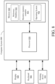
- FIG. 8 depicts an implementation of a computer system 800.
- the computer system 800 may include a processor 830 and a memory 840.
- the processor 830 which is coupled to the memory 840, may be any one or more suitable processors capable of executing scripts or instructions of one or more software programs stored within the computer system 800 (e.g., within the memory 840).
- the computer system 800 may be coupled to a display 820, a keyboard 822, and a pointing device 824.
- the memory 840 may be a solid state, magnetic, optical, magneto-optical, or any other suitable device capable of transient and/or non-volatile storage.
- the memory 840 may store a reference database 842.
- the reference database 842 may include design information associated one or more resistive memory arrays.
- the reference database 842 may include files describing a spin-transfer-torque, a spin-orbit-torque, or a carbon nanotube memory structure (e.g., files for one or more technology dependent arrangement of bit cells, sense amplifiers (amps), multiplexers, etc.).
- memory 840 may also include a non-transitory computer-readable storage medium (e.g., one or more nonvolatile memory elements, such as EPROM, EEPROM, Flash memory, a hard drive, etc.) that may include a resistive memory compiler 844 and an operating system 846.
- a non-transitory computer-readable storage medium e.g., one or more nonvolatile memory elements, such as EPROM, EEPROM, Flash memory, a hard drive, etc.
- a resistive memory compiler 844 e.g., one or more nonvolatile memory elements, such as EPROM, EEPROM, Flash memory, a hard drive, etc.
- the processor 830 may execute the operating system 846 to manage the computer system 800 hardware and provide services for execution of one or more computer programs.
- the processor 830 may execute the resistive memory compiler 844 to generate one or more output files (design files) associated with the MRAM array 300.
- the output files may include register transfer language (RTL) files and/or database files to instantiate the MRAM array 300 within a hierarchal or other suitable design.
- the output files may also include RTL and/or database files to instantiate memory reference bit lines and selectors (such as memory reference bit lines 320(1)-320(n) and reference bit line selectors 340(1)-340(n) described above with respect to FIG. 3 ).
- the processor 830 may be responsible for managing the bus and general processing, including the execution of software stored on machine-readable media (e.g., within the memory 840).
- the processor 830 may be implemented with one or more general-purpose and/or special-purpose processors. Examples include microprocessors, microcontrollers, DSP processors, and other circuitry that can execute software.
- Software shall be construed broadly to mean instructions, data, or any combination thereof, whether referred to as software, firmware, middleware, microcode, hardware description language, or otherwise.
- Machine-readable media may include, by way of example, RAM (Random Access Memory), flash memory, ROM (Read Only Memory), PROM (Programmable Read-Only Memory), EPROM (Erasable Programmable Read-Only Memory), EEPROM (Electrically Erasable Programmable Read-Only Memory), registers, magnetic disks, optical disks, hard drives, or any other suitable storage medium, or any combination thereof.
- RAM Random Access Memory
- ROM Read Only Memory
- PROM Programmable Read-Only Memory
- EPROM Erasable Programmable Read-Only Memory
- EEPROM Electrically Erasable Programmable Read-Only Memory
- registers magnetic disks, optical disks, hard drives, or any other suitable storage medium, or any combination thereof.
- the machine-readable media may be embodied in a computer-program product.
- the computer-program product may comprise packaging materials.
- DSP digital signal processor
- ASIC application specific integrated circuit
- FPGA field programmable gate array
- PLD programmable logic device
- a general-purpose processor may be a microprocessor, but in the alternative, the processor may be any commercially available processor, controller, microcontroller, or state machine.
- a processor may also be implemented as a combination of computing devices, e.g., a combination of a DSP and a microprocessor, a plurality of microprocessors, one or more microprocessors in conjunction with a DSP core, or any other such configuration.
- the functions described may be implemented in hardware, software, firmware, or any combination thereof.
- the processing system may be implemented with a bus architecture.
- the bus may include any number of interconnecting buses and bridges depending on the specific application of the processing system and the overall design constraints.
- the bus may link together various circuits including a processor, machine-readable media, and a bus interface.
- the bus interface may be used to connect a network adapter, among other things, to the processing system via the bus.
- the bus may also link various other circuits such as timing sources, peripherals, voltage regulators, power management circuits, and the like, which are well known in the art, and therefore, will not be described any further.
Landscapes
- Engineering & Computer Science (AREA)
- Computer Hardware Design (AREA)
- Power Engineering (AREA)
- Hall/Mr Elements (AREA)
- Mram Or Spin Memory Techniques (AREA)
Claims (10)
- Magnetisches Direktzugriffsspeicher (MRAM)-Array (300), das aufweist:mehrere Speicherdaten-Bitleitungsgruppen (310(1)-310(n)), die dazu ausgebildet sind, Daten zu speichern;mehrere Referenz-Bitleitungen (320(1)-320(n)), die dazu ausgebildet sind, eine Referenzspannung (Vref 360) bereitzustellen, wobei die Referenzspannung (Vref 360) auf Spannungen basiert, die durch zumindest eine resistive Bitzelle jeder Referenz-Bitleitung bereitgestellt werden; undmehrere Leseverstärker (350(1)-350(n)), die dazu ausgebildet sind, eine Datenbitleitungsspannung aus den mehreren Speicherdatenbitleitungsgruppen (310(1)-310(n)) mit der Referenzspannung zu vergleichen, wobei jede Referenzbitleitung benachbart zu einer entsprechenden Speicherdatenbitleitungsgruppe angeordnet ist.
- MRAM-Array (300) nach Anspruch 1, wobei die Referenzbitleitungen (320(1)-320(n)) eine erste Anzahl von resistiven Bitzellen aufweisen, die dazu ausgebildet sind, einen ersten logischen Zustand zu speichern, und eine zweite Anzahl von resistiven Bitzellen, die dazu ausgebildet sind, einen zweiten logischen Zustand zu speichern.
- MRAM-Array (300) nach Anspruch 2, wobei eine erste Spannung dem ersten logischen Zustand zugeordnet ist und eine zweite Spannung dem zweiten logischen Zustand zugeordnet ist.
- MRAM-Array (300) nach Anspruch 3, wobei die Referenzspannung (Vref 360) zwischen der dem ersten logischen Zustand zugeordneten ersten Spannung und der dem zweiten logischen Zustand zugeordneten zweiten Spannung liegt.
- MRAM-Array (300) nach Anspruch 2, wobei die mehreren Referenzbitleitungen (320(1)-320(n)) weiterhin dazu ausgebildet sind, eine Referenzspannung basierend auf der ersten Anzahl von resistiven Bitzellen und der zweiten Anzahl von resistiven Bitzellen bereitzustellen.
- MRAM-Array (300) nach Anspruch 2, wobei die erste Anzahl von resistiven Bitzellen gleich der zweiten Anzahl von resistiven Bitzellen ist.
- MRAM-Array (300) nach Anspruch 1, wobei die Referenzspannung (Vref 360) auf einem Durchschnitt von Spannungen basiert, die durch die zumindest eine resistive Bitzelle bereitgestellt werden.
- MRAM-Array (300) nach Anspruch 1, wobei jede Referenzbitleitung zumindest eine resistive Bitzelle enthält und jede Referenzbitleitung benachbart zu einer entsprechenden Speicherdatenbitleitungsgruppe angeordnet ist, einschließlich einer ersten Referenzbitleitung, die benachbart zu einer ersten Speicherdatenbitleitungsgruppe und benachbart zu einer zweiten Speicherdatenbitleitungsgruppe angeordnet ist, wobei die mehreren Speicherdatenbitleitungsgruppen (310(1)-310(n)) dazu ausgebildet sind, Daten in einer oder mehr resistiven Bitzellen zu speichern, wobei jede Datenbitleitungsgruppe dazu ausgebildet ist, einen einzelnen Bitvektor eines Datenworts zu bilden.
- MRAM-Array (300) nach Anspruch 1, das weiterhin aufweist: einen Multiplexer, der dazu ausgebildet ist, zumindest eine Datenbitleitung aus den mehreren Speicherdatenbitleitungsgruppen (310(1)-310(n)) auszuwählen und eine Datenbitleitung aus den Speicherdatenbitleitungsgruppen (310(1)-310(n)) mit einem Leseverstärker der mehreren Leseverstärker (350(1)- 350(n)) zu koppeln.
- MRAM-Array (300) nach Anspruch 1, wobei die Referenzspannung (Vref 360) im Wesentlichen in der Mitte zwischen einer Spannungsverteilung, die einem ersten logischen Zustand einer resistiven Bitzelle zugeordnet ist, und einer Spannungsverteilung, die einem zweiten logischen Zustand der resistiven Bitzelle zugeordnet ist, liegt.
Priority Applications (1)
| Application Number | Priority Date | Filing Date | Title |
|---|---|---|---|
| EP23185744.2A EP4235668A3 (de) | 2017-11-02 | 2018-11-02 | Referenzspannungsgenerator für resistive speichermatrix |
Applications Claiming Priority (2)
| Application Number | Priority Date | Filing Date | Title |
|---|---|---|---|
| US201762580968P | 2017-11-02 | 2017-11-02 | |
| PCT/US2018/059076 WO2019090162A1 (en) | 2017-11-02 | 2018-11-02 | Reference voltage generator for resistive memory array |
Related Child Applications (1)
| Application Number | Title | Priority Date | Filing Date |
|---|---|---|---|
| EP23185744.2A Division EP4235668A3 (de) | 2017-11-02 | 2018-11-02 | Referenzspannungsgenerator für resistive speichermatrix |
Publications (4)
| Publication Number | Publication Date |
|---|---|
| EP3704697A1 EP3704697A1 (de) | 2020-09-09 |
| EP3704697A4 EP3704697A4 (de) | 2021-11-03 |
| EP3704697C0 EP3704697C0 (de) | 2023-08-16 |
| EP3704697B1 true EP3704697B1 (de) | 2023-08-16 |
Family
ID=66244231
Family Applications (2)
| Application Number | Title | Priority Date | Filing Date |
|---|---|---|---|
| EP18872763.0A Active EP3704697B1 (de) | 2017-11-02 | 2018-11-02 | Referenzspannungsgenerator für widerstandsspeicheranordnung |
| EP23185744.2A Withdrawn EP4235668A3 (de) | 2017-11-02 | 2018-11-02 | Referenzspannungsgenerator für resistive speichermatrix |
Family Applications After (1)
| Application Number | Title | Priority Date | Filing Date |
|---|---|---|---|
| EP23185744.2A Withdrawn EP4235668A3 (de) | 2017-11-02 | 2018-11-02 | Referenzspannungsgenerator für resistive speichermatrix |
Country Status (4)
| Country | Link |
|---|---|
| US (1) | US10726880B2 (de) |
| EP (2) | EP3704697B1 (de) |
| CN (1) | CN111316357B (de) |
| WO (1) | WO2019090162A1 (de) |
Families Citing this family (3)
| Publication number | Priority date | Publication date | Assignee | Title |
|---|---|---|---|---|
| JP2018147532A (ja) * | 2017-03-03 | 2018-09-20 | ソニーセミコンダクタソリューションズ株式会社 | 半導体記憶装置及び情報処理装置 |
| US11705176B2 (en) * | 2020-08-07 | 2023-07-18 | Tohoku University | Storage circuit provided with variable resistance type elements, and its test device |
| JP7677611B2 (ja) | 2021-03-03 | 2025-05-15 | 国立大学法人東北大学 | 抵抗変化型素子を備えた記憶回路 |
Family Cites Families (26)
| Publication number | Priority date | Publication date | Assignee | Title |
|---|---|---|---|---|
| US6055178A (en) | 1998-12-18 | 2000-04-25 | Motorola, Inc. | Magnetic random access memory with a reference memory array |
| JP4407828B2 (ja) | 2003-04-21 | 2010-02-03 | 日本電気株式会社 | データの読み出し方法が改善された磁気ランダムアクセスメモリ |
| US7099193B2 (en) | 2003-09-08 | 2006-08-29 | Kabushiki Kaisha Toshiba | Nonvolatile semiconductor memory device, electronic card and electronic apparatus |
| KR100590767B1 (ko) | 2003-12-17 | 2006-06-15 | 한국전자통신연구원 | 기능 블럭을 용이하게 구성할 수 있는 소프트아이피의의존성 사양 파일 생성 방법 및 이 기능을 실현하는 기록매체 |
| KR100558012B1 (ko) | 2004-07-16 | 2006-03-06 | 삼성전자주식회사 | 반도체 메모리 소자 |
| US8202561B2 (en) * | 2005-09-16 | 2012-06-19 | Mott's Llp | Tomato-based alcohol compositions and methods of preparation |
| JP2007164969A (ja) | 2005-12-15 | 2007-06-28 | Samsung Electronics Co Ltd | 選択された基準メモリセルを具備する抵抗型メモリ素子 |
| US7733718B2 (en) * | 2007-07-04 | 2010-06-08 | Hynix Semiconductor, Inc. | One-transistor type DRAM |
| KR100887061B1 (ko) | 2007-07-24 | 2009-03-04 | 주식회사 하이닉스반도체 | 상 변화 메모리 장치 |
| US7881094B2 (en) | 2008-11-12 | 2011-02-01 | Seagate Technology Llc | Voltage reference generation for resistive sense memory cells |
| US8437171B1 (en) | 2009-12-31 | 2013-05-07 | Adesto Technologies Corporation | Methods and circuits for temperature varying write operations of programmable impedance elements |
| US8434032B2 (en) | 2010-11-19 | 2013-04-30 | Taiwan Semiconductor Maufacturing Company, Ltd. | Method of generating an intellectual property block design kit, method of generating an integrated circuit design, and simulation system for the integrated circuit design |
| US8665638B2 (en) * | 2011-07-11 | 2014-03-04 | Qualcomm Incorporated | MRAM sensing with magnetically annealed reference cell |
| US8780657B2 (en) * | 2012-03-01 | 2014-07-15 | Apple Inc. | Memory with bit line current injection |
| US8902641B2 (en) * | 2012-04-10 | 2014-12-02 | Taiwan Semiconductor Manufacturing Co., Ltd. | Adjusting reference resistances in determining MRAM resistance states |
| US9147457B2 (en) * | 2012-09-13 | 2015-09-29 | Qualcomm Incorporated | Reference cell repair scheme |
| KR102060488B1 (ko) * | 2012-12-27 | 2019-12-30 | 삼성전자주식회사 | 불휘발성 랜덤 액세스 메모리 장치 및 그것의 데이터 읽기 방법 |
| US9165629B2 (en) * | 2013-03-12 | 2015-10-20 | Taiwan Semiconductor Manufacturing Co., Ltd. | Method and apparatus for MRAM sense reference trimming |
| KR102187116B1 (ko) * | 2014-04-07 | 2020-12-04 | 삼성전자주식회사 | 비휘발성 메모리 장치와 이를 포함하는 메모리 시스템, 및 비휘발성 메모리 장치의 구동 방법 |
| WO2016068911A1 (en) | 2014-10-29 | 2016-05-06 | Hewlett Packard Enterprise Development Lp | Resistive memory device |
| US9373395B1 (en) * | 2015-03-04 | 2016-06-21 | Intel Corporation | Apparatus to reduce retention failure in complementary resistive memory |
| US9704541B2 (en) | 2015-06-12 | 2017-07-11 | Micron Technology, Inc. | Simulating access lines |
| US10747921B2 (en) | 2016-01-05 | 2020-08-18 | Cyient, Inc. | Software tool for simulating operation of hardware and software systems |
| US9659624B1 (en) * | 2016-03-15 | 2017-05-23 | Avago Technologies General Ip (Singapore) Pte. Ltd. | Method for sense reference generation for MTJ based memories |
| US9576653B1 (en) * | 2016-05-10 | 2017-02-21 | Taiwan Semiconductor Manufacturing Co., Ltd. | Fast sense amplifier with bit-line pre-charging |
| US10430534B2 (en) | 2016-11-30 | 2019-10-01 | Numem Inc. | Resistance-based memory compiler |
-
2018
- 2018-11-02 WO PCT/US2018/059076 patent/WO2019090162A1/en not_active Ceased
- 2018-11-02 EP EP18872763.0A patent/EP3704697B1/de active Active
- 2018-11-02 EP EP23185744.2A patent/EP4235668A3/de not_active Withdrawn
- 2018-11-02 CN CN201880071320.2A patent/CN111316357B/zh active Active
- 2018-11-02 US US16/179,739 patent/US10726880B2/en active Active
Also Published As
| Publication number | Publication date |
|---|---|
| EP4235668A3 (de) | 2023-12-06 |
| EP3704697A4 (de) | 2021-11-03 |
| EP3704697A1 (de) | 2020-09-09 |
| US20190130945A1 (en) | 2019-05-02 |
| WO2019090162A1 (en) | 2019-05-09 |
| CN111316357A (zh) | 2020-06-19 |
| EP3704697C0 (de) | 2023-08-16 |
| CN111316357B (zh) | 2022-03-15 |
| US10726880B2 (en) | 2020-07-28 |
| EP4235668A2 (de) | 2023-08-30 |
Similar Documents
| Publication | Publication Date | Title |
|---|---|---|
| US10460056B2 (en) | Resistance-based memory compiler | |
| US11721399B2 (en) | Memory system with dynamic calibration using a trim management mechanism | |
| KR101787223B1 (ko) | 워드라인 전압 증가 보상용 장치, 감지 회로, 및 방법 | |
| US8929127B2 (en) | Current generator for nonvolatile memory device and write and/or read currents calibrating method using the same | |
| US10395734B2 (en) | Method and apparatus for determining a cell state of a resistive memory cell | |
| EP3704697B1 (de) | Referenzspannungsgenerator für widerstandsspeicheranordnung | |
| US9953706B2 (en) | Method and apparatus for faster determination of cell state of a resistive memory cell using a parallel resistor | |
| CN109872751B (zh) | 存储器装置及其操作方法 | |
| WO2019133328A1 (en) | Memory array with individually trimmable sense amplifiers | |
| US20110096587A1 (en) | Dynamic sense current supply circuit and associated method for reading and characterizing a resistive memory array | |
| US10224088B1 (en) | Memory with a global reference circuit | |
| US11442877B2 (en) | Data bus duty cycle distortion compensation | |
| JPWO2013128854A1 (ja) | 不揮発性半導体記憶装置 | |
| US12131787B2 (en) | Page buffer counting for in-memory search | |
| US20230367497A1 (en) | Memory system, operating method and controller | |
| CN117079685A (zh) | 写操作电路和存储器 |
Legal Events
| Date | Code | Title | Description |
|---|---|---|---|
| STAA | Information on the status of an ep patent application or granted ep patent |
Free format text: STATUS: THE INTERNATIONAL PUBLICATION HAS BEEN MADE |
|
| PUAI | Public reference made under article 153(3) epc to a published international application that has entered the european phase |
Free format text: ORIGINAL CODE: 0009012 |
|
| STAA | Information on the status of an ep patent application or granted ep patent |
Free format text: STATUS: REQUEST FOR EXAMINATION WAS MADE |
|
| 17P | Request for examination filed |
Effective date: 20200601 |
|
| AK | Designated contracting states |
Kind code of ref document: A1 Designated state(s): AL AT BE BG CH CY CZ DE DK EE ES FI FR GB GR HR HU IE IS IT LI LT LU LV MC MK MT NL NO PL PT RO RS SE SI SK SM TR |
|
| AX | Request for extension of the european patent |
Extension state: BA ME |
|
| DAV | Request for validation of the european patent (deleted) | ||
| DAX | Request for extension of the european patent (deleted) | ||
| REG | Reference to a national code |
Ref country code: DE Ref legal event code: R079 Ref document number: 602018055678 Country of ref document: DE Free format text: PREVIOUS MAIN CLASS: G11C0007020000 Ipc: G11C0011160000 Ref country code: DE Ref legal event code: R079 Free format text: PREVIOUS MAIN CLASS: G11C0007020000 Ipc: G11C0011160000 |
|
| A4 | Supplementary search report drawn up and despatched |
Effective date: 20211001 |
|
| RIC1 | Information provided on ipc code assigned before grant |
Ipc: G11C 11/15 20060101ALI20210927BHEP Ipc: G11C 11/14 20060101ALI20210927BHEP Ipc: G11C 11/02 20060101ALI20210927BHEP Ipc: G11C 11/00 20060101ALI20210927BHEP Ipc: G11C 7/02 20060101ALI20210927BHEP Ipc: G11C 11/16 20060101AFI20210927BHEP |
|
| STAA | Information on the status of an ep patent application or granted ep patent |
Free format text: STATUS: EXAMINATION IS IN PROGRESS |
|
| 17Q | First examination report despatched |
Effective date: 20220719 |
|
| GRAP | Despatch of communication of intention to grant a patent |
Free format text: ORIGINAL CODE: EPIDOSNIGR1 |
|
| STAA | Information on the status of an ep patent application or granted ep patent |
Free format text: STATUS: GRANT OF PATENT IS INTENDED |
|
| INTG | Intention to grant announced |
Effective date: 20230426 |
|
| GRAS | Grant fee paid |
Free format text: ORIGINAL CODE: EPIDOSNIGR3 |
|
| GRAA | (expected) grant |
Free format text: ORIGINAL CODE: 0009210 |
|
| STAA | Information on the status of an ep patent application or granted ep patent |
Free format text: STATUS: THE PATENT HAS BEEN GRANTED |
|
| AK | Designated contracting states |
Kind code of ref document: B1 Designated state(s): AL AT BE BG CH CY CZ DE DK EE ES FI FR GB GR HR HU IE IS IT LI LT LU LV MC MK MT NL NO PL PT RO RS SE SI SK SM TR |
|
| REG | Reference to a national code |
Ref country code: CH Ref legal event code: EP Ref country code: DE Ref legal event code: R096 Ref document number: 602018055678 Country of ref document: DE |
|
| REG | Reference to a national code |
Ref country code: IE Ref legal event code: FG4D |
|
| U01 | Request for unitary effect filed |
Effective date: 20230816 |
|
| U07 | Unitary effect registered |
Designated state(s): AT BE BG DE DK EE FI FR IT LT LU LV MT NL PT SE SI Effective date: 20230822 |
|
| U20 | Renewal fee for the european patent with unitary effect paid |
Year of fee payment: 6 Effective date: 20231122 |
|
| PG25 | Lapsed in a contracting state [announced via postgrant information from national office to epo] |
Ref country code: GR Free format text: LAPSE BECAUSE OF FAILURE TO SUBMIT A TRANSLATION OF THE DESCRIPTION OR TO PAY THE FEE WITHIN THE PRESCRIBED TIME-LIMIT Effective date: 20231117 |
|
| PG25 | Lapsed in a contracting state [announced via postgrant information from national office to epo] |
Ref country code: IS Free format text: LAPSE BECAUSE OF FAILURE TO SUBMIT A TRANSLATION OF THE DESCRIPTION OR TO PAY THE FEE WITHIN THE PRESCRIBED TIME-LIMIT Effective date: 20231216 |
|
| PG25 | Lapsed in a contracting state [announced via postgrant information from national office to epo] |
Ref country code: RS Free format text: LAPSE BECAUSE OF FAILURE TO SUBMIT A TRANSLATION OF THE DESCRIPTION OR TO PAY THE FEE WITHIN THE PRESCRIBED TIME-LIMIT Effective date: 20230816 Ref country code: NO Free format text: LAPSE BECAUSE OF FAILURE TO SUBMIT A TRANSLATION OF THE DESCRIPTION OR TO PAY THE FEE WITHIN THE PRESCRIBED TIME-LIMIT Effective date: 20231116 Ref country code: IS Free format text: LAPSE BECAUSE OF FAILURE TO SUBMIT A TRANSLATION OF THE DESCRIPTION OR TO PAY THE FEE WITHIN THE PRESCRIBED TIME-LIMIT Effective date: 20231216 Ref country code: HR Free format text: LAPSE BECAUSE OF FAILURE TO SUBMIT A TRANSLATION OF THE DESCRIPTION OR TO PAY THE FEE WITHIN THE PRESCRIBED TIME-LIMIT Effective date: 20230816 Ref country code: GR Free format text: LAPSE BECAUSE OF FAILURE TO SUBMIT A TRANSLATION OF THE DESCRIPTION OR TO PAY THE FEE WITHIN THE PRESCRIBED TIME-LIMIT Effective date: 20231117 |
|
| PG25 | Lapsed in a contracting state [announced via postgrant information from national office to epo] |
Ref country code: PL Free format text: LAPSE BECAUSE OF FAILURE TO SUBMIT A TRANSLATION OF THE DESCRIPTION OR TO PAY THE FEE WITHIN THE PRESCRIBED TIME-LIMIT Effective date: 20230816 |
|
| PG25 | Lapsed in a contracting state [announced via postgrant information from national office to epo] |
Ref country code: ES Free format text: LAPSE BECAUSE OF FAILURE TO SUBMIT A TRANSLATION OF THE DESCRIPTION OR TO PAY THE FEE WITHIN THE PRESCRIBED TIME-LIMIT Effective date: 20230816 |
|
| PG25 | Lapsed in a contracting state [announced via postgrant information from national office to epo] |
Ref country code: SM Free format text: LAPSE BECAUSE OF FAILURE TO SUBMIT A TRANSLATION OF THE DESCRIPTION OR TO PAY THE FEE WITHIN THE PRESCRIBED TIME-LIMIT Effective date: 20230816 Ref country code: RO Free format text: LAPSE BECAUSE OF FAILURE TO SUBMIT A TRANSLATION OF THE DESCRIPTION OR TO PAY THE FEE WITHIN THE PRESCRIBED TIME-LIMIT Effective date: 20230816 Ref country code: ES Free format text: LAPSE BECAUSE OF FAILURE TO SUBMIT A TRANSLATION OF THE DESCRIPTION OR TO PAY THE FEE WITHIN THE PRESCRIBED TIME-LIMIT Effective date: 20230816 Ref country code: CZ Free format text: LAPSE BECAUSE OF FAILURE TO SUBMIT A TRANSLATION OF THE DESCRIPTION OR TO PAY THE FEE WITHIN THE PRESCRIBED TIME-LIMIT Effective date: 20230816 Ref country code: SK Free format text: LAPSE BECAUSE OF FAILURE TO SUBMIT A TRANSLATION OF THE DESCRIPTION OR TO PAY THE FEE WITHIN THE PRESCRIBED TIME-LIMIT Effective date: 20230816 |
|
| PLBE | No opposition filed within time limit |
Free format text: ORIGINAL CODE: 0009261 |
|
| STAA | Information on the status of an ep patent application or granted ep patent |
Free format text: STATUS: NO OPPOSITION FILED WITHIN TIME LIMIT |
|
| REG | Reference to a national code |
Ref country code: CH Ref legal event code: PL |
|
| PG25 | Lapsed in a contracting state [announced via postgrant information from national office to epo] |
Ref country code: MC Free format text: LAPSE BECAUSE OF FAILURE TO SUBMIT A TRANSLATION OF THE DESCRIPTION OR TO PAY THE FEE WITHIN THE PRESCRIBED TIME-LIMIT Effective date: 20230816 |
|
| PG25 | Lapsed in a contracting state [announced via postgrant information from national office to epo] |
Ref country code: CH Free format text: LAPSE BECAUSE OF NON-PAYMENT OF DUE FEES Effective date: 20231130 |
|
| 26N | No opposition filed |
Effective date: 20240517 |
|
| PG25 | Lapsed in a contracting state [announced via postgrant information from national office to epo] |
Ref country code: MC Free format text: LAPSE BECAUSE OF FAILURE TO SUBMIT A TRANSLATION OF THE DESCRIPTION OR TO PAY THE FEE WITHIN THE PRESCRIBED TIME-LIMIT Effective date: 20230816 Ref country code: CH Free format text: LAPSE BECAUSE OF NON-PAYMENT OF DUE FEES Effective date: 20231130 |
|
| REG | Reference to a national code |
Ref country code: IE Ref legal event code: MM4A |
|
| PG25 | Lapsed in a contracting state [announced via postgrant information from national office to epo] |
Ref country code: IE Free format text: LAPSE BECAUSE OF NON-PAYMENT OF DUE FEES Effective date: 20231102 |
|
| PG25 | Lapsed in a contracting state [announced via postgrant information from national office to epo] |
Ref country code: IE Free format text: LAPSE BECAUSE OF NON-PAYMENT OF DUE FEES Effective date: 20231102 |
|
| U20 | Renewal fee for the european patent with unitary effect paid |
Year of fee payment: 7 Effective date: 20241031 |
|
| PGFP | Annual fee paid to national office [announced via postgrant information from national office to epo] |
Ref country code: GB Payment date: 20241106 Year of fee payment: 7 |
|
| PG25 | Lapsed in a contracting state [announced via postgrant information from national office to epo] |
Ref country code: CY Free format text: LAPSE BECAUSE OF FAILURE TO SUBMIT A TRANSLATION OF THE DESCRIPTION OR TO PAY THE FEE WITHIN THE PRESCRIBED TIME-LIMIT; INVALID AB INITIO Effective date: 20181102 |
|
| PG25 | Lapsed in a contracting state [announced via postgrant information from national office to epo] |
Ref country code: HU Free format text: LAPSE BECAUSE OF FAILURE TO SUBMIT A TRANSLATION OF THE DESCRIPTION OR TO PAY THE FEE WITHIN THE PRESCRIBED TIME-LIMIT; INVALID AB INITIO Effective date: 20181102 |
|
| PG25 | Lapsed in a contracting state [announced via postgrant information from national office to epo] |
Ref country code: TR Free format text: LAPSE BECAUSE OF FAILURE TO SUBMIT A TRANSLATION OF THE DESCRIPTION OR TO PAY THE FEE WITHIN THE PRESCRIBED TIME-LIMIT Effective date: 20230816 |