EP3702792B1 - Verfahren zur herstellung einer sonde für die rastersondenmikroskopie - Google Patents
Verfahren zur herstellung einer sonde für die rastersondenmikroskopie Download PDFInfo
- Publication number
- EP3702792B1 EP3702792B1 EP19160202.8A EP19160202A EP3702792B1 EP 3702792 B1 EP3702792 B1 EP 3702792B1 EP 19160202 A EP19160202 A EP 19160202A EP 3702792 B1 EP3702792 B1 EP 3702792B1
- Authority
- EP
- European Patent Office
- Prior art keywords
- tip
- layer
- etch
- probe
- tip body
- Prior art date
- Legal status (The legal status is an assumption and is not a legal conclusion. Google has not performed a legal analysis and makes no representation as to the accuracy of the status listed.)
- Active
Links
Images


Classifications
-
- G—PHYSICS
- G01—MEASURING; TESTING
- G01Q—SCANNING-PROBE TECHNIQUES OR APPARATUS; APPLICATIONS OF SCANNING-PROBE TECHNIQUES, e.g. SCANNING PROBE MICROSCOPY [SPM]
- G01Q70/00—General aspects of SPM probes, their manufacture or their related instrumentation, insofar as they are not specially adapted to a single SPM technique covered by group G01Q60/00
- G01Q70/08—Probe characteristics
- G01Q70/10—Shape or taper
-
- C—CHEMISTRY; METALLURGY
- C23—COATING METALLIC MATERIAL; COATING MATERIAL WITH METALLIC MATERIAL; CHEMICAL SURFACE TREATMENT; DIFFUSION TREATMENT OF METALLIC MATERIAL; COATING BY VACUUM EVAPORATION, BY SPUTTERING, BY ION IMPLANTATION OR BY CHEMICAL VAPOUR DEPOSITION, IN GENERAL; INHIBITING CORROSION OF METALLIC MATERIAL OR INCRUSTATION IN GENERAL
- C23C—COATING METALLIC MATERIAL; COATING MATERIAL WITH METALLIC MATERIAL; SURFACE TREATMENT OF METALLIC MATERIAL BY DIFFUSION INTO THE SURFACE, BY CHEMICAL CONVERSION OR SUBSTITUTION; COATING BY VACUUM EVAPORATION, BY SPUTTERING, BY ION IMPLANTATION OR BY CHEMICAL VAPOUR DEPOSITION, IN GENERAL
- C23C16/00—Chemical coating by decomposition of gaseous compounds, without leaving reaction products of surface material in the coating, i.e. chemical vapour deposition [CVD] processes
- C23C16/02—Pretreatment of the material to be coated
- C23C16/0272—Deposition of sub-layers, e.g. to promote the adhesion of the main coating
-
- C—CHEMISTRY; METALLURGY
- C23—COATING METALLIC MATERIAL; COATING MATERIAL WITH METALLIC MATERIAL; CHEMICAL SURFACE TREATMENT; DIFFUSION TREATMENT OF METALLIC MATERIAL; COATING BY VACUUM EVAPORATION, BY SPUTTERING, BY ION IMPLANTATION OR BY CHEMICAL VAPOUR DEPOSITION, IN GENERAL; INHIBITING CORROSION OF METALLIC MATERIAL OR INCRUSTATION IN GENERAL
- C23C—COATING METALLIC MATERIAL; COATING MATERIAL WITH METALLIC MATERIAL; SURFACE TREATMENT OF METALLIC MATERIAL BY DIFFUSION INTO THE SURFACE, BY CHEMICAL CONVERSION OR SUBSTITUTION; COATING BY VACUUM EVAPORATION, BY SPUTTERING, BY ION IMPLANTATION OR BY CHEMICAL VAPOUR DEPOSITION, IN GENERAL
- C23C16/00—Chemical coating by decomposition of gaseous compounds, without leaving reaction products of surface material in the coating, i.e. chemical vapour deposition [CVD] processes
- C23C16/04—Coating on selected surface areas, e.g. using masks
- C23C16/045—Coating cavities or hollow spaces, e.g. interior of tubes; Infiltration of porous substrates
-
- C—CHEMISTRY; METALLURGY
- C23—COATING METALLIC MATERIAL; COATING MATERIAL WITH METALLIC MATERIAL; CHEMICAL SURFACE TREATMENT; DIFFUSION TREATMENT OF METALLIC MATERIAL; COATING BY VACUUM EVAPORATION, BY SPUTTERING, BY ION IMPLANTATION OR BY CHEMICAL VAPOUR DEPOSITION, IN GENERAL; INHIBITING CORROSION OF METALLIC MATERIAL OR INCRUSTATION IN GENERAL
- C23C—COATING METALLIC MATERIAL; COATING MATERIAL WITH METALLIC MATERIAL; SURFACE TREATMENT OF METALLIC MATERIAL BY DIFFUSION INTO THE SURFACE, BY CHEMICAL CONVERSION OR SUBSTITUTION; COATING BY VACUUM EVAPORATION, BY SPUTTERING, BY ION IMPLANTATION OR BY CHEMICAL VAPOUR DEPOSITION, IN GENERAL
- C23C16/00—Chemical coating by decomposition of gaseous compounds, without leaving reaction products of surface material in the coating, i.e. chemical vapour deposition [CVD] processes
- C23C16/22—Chemical coating by decomposition of gaseous compounds, without leaving reaction products of surface material in the coating, i.e. chemical vapour deposition [CVD] processes characterised by the deposition of inorganic material, other than metallic material
- C23C16/26—Deposition of carbon only
- C23C16/27—Diamond only
- C23C16/278—Diamond only doping or introduction of a secondary phase in the diamond
-
- C—CHEMISTRY; METALLURGY
- C23—COATING METALLIC MATERIAL; COATING MATERIAL WITH METALLIC MATERIAL; CHEMICAL SURFACE TREATMENT; DIFFUSION TREATMENT OF METALLIC MATERIAL; COATING BY VACUUM EVAPORATION, BY SPUTTERING, BY ION IMPLANTATION OR BY CHEMICAL VAPOUR DEPOSITION, IN GENERAL; INHIBITING CORROSION OF METALLIC MATERIAL OR INCRUSTATION IN GENERAL
- C23C—COATING METALLIC MATERIAL; COATING MATERIAL WITH METALLIC MATERIAL; SURFACE TREATMENT OF METALLIC MATERIAL BY DIFFUSION INTO THE SURFACE, BY CHEMICAL CONVERSION OR SUBSTITUTION; COATING BY VACUUM EVAPORATION, BY SPUTTERING, BY ION IMPLANTATION OR BY CHEMICAL VAPOUR DEPOSITION, IN GENERAL
- C23C16/00—Chemical coating by decomposition of gaseous compounds, without leaving reaction products of surface material in the coating, i.e. chemical vapour deposition [CVD] processes
- C23C16/22—Chemical coating by decomposition of gaseous compounds, without leaving reaction products of surface material in the coating, i.e. chemical vapour deposition [CVD] processes characterised by the deposition of inorganic material, other than metallic material
- C23C16/30—Deposition of compounds, mixtures or solid solutions, e.g. borides, carbides, nitrides
-
- C—CHEMISTRY; METALLURGY
- C23—COATING METALLIC MATERIAL; COATING MATERIAL WITH METALLIC MATERIAL; CHEMICAL SURFACE TREATMENT; DIFFUSION TREATMENT OF METALLIC MATERIAL; COATING BY VACUUM EVAPORATION, BY SPUTTERING, BY ION IMPLANTATION OR BY CHEMICAL VAPOUR DEPOSITION, IN GENERAL; INHIBITING CORROSION OF METALLIC MATERIAL OR INCRUSTATION IN GENERAL
- C23C—COATING METALLIC MATERIAL; COATING MATERIAL WITH METALLIC MATERIAL; SURFACE TREATMENT OF METALLIC MATERIAL BY DIFFUSION INTO THE SURFACE, BY CHEMICAL CONVERSION OR SUBSTITUTION; COATING BY VACUUM EVAPORATION, BY SPUTTERING, BY ION IMPLANTATION OR BY CHEMICAL VAPOUR DEPOSITION, IN GENERAL
- C23C16/00—Chemical coating by decomposition of gaseous compounds, without leaving reaction products of surface material in the coating, i.e. chemical vapour deposition [CVD] processes
- C23C16/56—After-treatment
-
- C—CHEMISTRY; METALLURGY
- C30—CRYSTAL GROWTH
- C30B—SINGLE-CRYSTAL GROWTH; UNIDIRECTIONAL SOLIDIFICATION OF EUTECTIC MATERIAL OR UNIDIRECTIONAL DEMIXING OF EUTECTOID MATERIAL; REFINING BY ZONE-MELTING OF MATERIAL; PRODUCTION OF A HOMOGENEOUS POLYCRYSTALLINE MATERIAL WITH DEFINED STRUCTURE; SINGLE CRYSTALS OR HOMOGENEOUS POLYCRYSTALLINE MATERIAL WITH DEFINED STRUCTURE; AFTER-TREATMENT OF SINGLE CRYSTALS OR A HOMOGENEOUS POLYCRYSTALLINE MATERIAL WITH DEFINED STRUCTURE; APPARATUS THEREFOR
- C30B25/00—Single-crystal growth by chemical reaction of reactive gases, e.g. chemical vapour-deposition growth
- C30B25/02—Epitaxial-layer growth
- C30B25/04—Pattern deposit, e.g. by using masks
-
- C—CHEMISTRY; METALLURGY
- C30—CRYSTAL GROWTH
- C30B—SINGLE-CRYSTAL GROWTH; UNIDIRECTIONAL SOLIDIFICATION OF EUTECTIC MATERIAL OR UNIDIRECTIONAL DEMIXING OF EUTECTOID MATERIAL; REFINING BY ZONE-MELTING OF MATERIAL; PRODUCTION OF A HOMOGENEOUS POLYCRYSTALLINE MATERIAL WITH DEFINED STRUCTURE; SINGLE CRYSTALS OR HOMOGENEOUS POLYCRYSTALLINE MATERIAL WITH DEFINED STRUCTURE; AFTER-TREATMENT OF SINGLE CRYSTALS OR A HOMOGENEOUS POLYCRYSTALLINE MATERIAL WITH DEFINED STRUCTURE; APPARATUS THEREFOR
- C30B25/00—Single-crystal growth by chemical reaction of reactive gases, e.g. chemical vapour-deposition growth
- C30B25/02—Epitaxial-layer growth
- C30B25/18—Epitaxial-layer growth characterised by the substrate
-
- C—CHEMISTRY; METALLURGY
- C30—CRYSTAL GROWTH
- C30B—SINGLE-CRYSTAL GROWTH; UNIDIRECTIONAL SOLIDIFICATION OF EUTECTIC MATERIAL OR UNIDIRECTIONAL DEMIXING OF EUTECTOID MATERIAL; REFINING BY ZONE-MELTING OF MATERIAL; PRODUCTION OF A HOMOGENEOUS POLYCRYSTALLINE MATERIAL WITH DEFINED STRUCTURE; SINGLE CRYSTALS OR HOMOGENEOUS POLYCRYSTALLINE MATERIAL WITH DEFINED STRUCTURE; AFTER-TREATMENT OF SINGLE CRYSTALS OR A HOMOGENEOUS POLYCRYSTALLINE MATERIAL WITH DEFINED STRUCTURE; APPARATUS THEREFOR
- C30B29/00—Single crystals or homogeneous polycrystalline material with defined structure characterised by the material or by their shape
- C30B29/02—Elements
- C30B29/04—Diamond
-
- C—CHEMISTRY; METALLURGY
- C30—CRYSTAL GROWTH
- C30B—SINGLE-CRYSTAL GROWTH; UNIDIRECTIONAL SOLIDIFICATION OF EUTECTIC MATERIAL OR UNIDIRECTIONAL DEMIXING OF EUTECTOID MATERIAL; REFINING BY ZONE-MELTING OF MATERIAL; PRODUCTION OF A HOMOGENEOUS POLYCRYSTALLINE MATERIAL WITH DEFINED STRUCTURE; SINGLE CRYSTALS OR HOMOGENEOUS POLYCRYSTALLINE MATERIAL WITH DEFINED STRUCTURE; AFTER-TREATMENT OF SINGLE CRYSTALS OR A HOMOGENEOUS POLYCRYSTALLINE MATERIAL WITH DEFINED STRUCTURE; APPARATUS THEREFOR
- C30B33/00—After-treatment of single crystals or homogeneous polycrystalline material with defined structure
- C30B33/08—Etching
- C30B33/12—Etching in gas atmosphere or plasma
-
- G—PHYSICS
- G01—MEASURING; TESTING
- G01Q—SCANNING-PROBE TECHNIQUES OR APPARATUS; APPLICATIONS OF SCANNING-PROBE TECHNIQUES, e.g. SCANNING PROBE MICROSCOPY [SPM]
- G01Q70/00—General aspects of SPM probes, their manufacture or their related instrumentation, insofar as they are not specially adapted to a single SPM technique covered by group G01Q60/00
- G01Q70/06—Probe tip arrays
-
- G—PHYSICS
- G01—MEASURING; TESTING
- G01Q—SCANNING-PROBE TECHNIQUES OR APPARATUS; APPLICATIONS OF SCANNING-PROBE TECHNIQUES, e.g. SCANNING PROBE MICROSCOPY [SPM]
- G01Q70/00—General aspects of SPM probes, their manufacture or their related instrumentation, insofar as they are not specially adapted to a single SPM technique covered by group G01Q60/00
- G01Q70/08—Probe characteristics
- G01Q70/14—Particular materials
-
- G—PHYSICS
- G01—MEASURING; TESTING
- G01Q—SCANNING-PROBE TECHNIQUES OR APPARATUS; APPLICATIONS OF SCANNING-PROBE TECHNIQUES, e.g. SCANNING PROBE MICROSCOPY [SPM]
- G01Q10/00—Scanning or positioning arrangements, i.e. arrangements for actively controlling the movement or position of the probe
- G01Q10/04—Fine scanning or positioning
- G01Q10/045—Self-actuating probes, i.e. wherein the actuating means for driving are part of the probe itself, e.g. piezoelectric means on a cantilever probe
-
- G—PHYSICS
- G01—MEASURING; TESTING
- G01Q—SCANNING-PROBE TECHNIQUES OR APPARATUS; APPLICATIONS OF SCANNING-PROBE TECHNIQUES, e.g. SCANNING PROBE MICROSCOPY [SPM]
- G01Q60/00—Particular types of SPM [Scanning Probe Microscopy] or microscopes; Essential components thereof
- G01Q60/02—Multiple-type SPM, i.e. involving more than one SPM techniques
Definitions
- the present invention is related to probes suitable for scanning probe microscopy (SPM) techniques such as atomic force microscopy (AFM) or scanning spreading resistance microscopy (SSRM).
- SPM scanning probe microscopy
- AFM atomic force microscopy
- SSRM scanning spreading resistance microscopy
- An SPM probe comprises an elongate strip attached at one end to a holder and carrying at its other end a tip.
- the strip is referred to as the cantilever of the probe, while the tip may be a pyramid-shaped body placed onto the plane of the cantilever as illustrated for example in document US5221415 , thereby pointing in a direction essentially perpendicular to the cantilever.
- the tip may extend in the plane of the cantilever, as illustrated for example in document US8484761 , or the tip may extend from the cantilever at an angle between 0 and 90 degrees.
- the tip is placed in contact to or in close proximity with a surface and the probe is scanned along a given trajectory, usually a set of parallel lines.
- the interaction between the tip and the surface is translated into topographical, electrical or magnetic data of the surface, or into signals related to the composition of a sample, depending on the characteristics of the tip.
- the probe may be in continuous contact with the surface under investigation, or an intermittent contact mode may be applied, wherein the surface characteristics are measured by detecting changes in the impedance (electrical or other) of the probe-surface connection.
- a contactless mode is equally applicable, when the interaction between the probe and the surface is dominated by non-contact forces such as Vanderwaals forces.
- the document ⁇ Diamond-modified AFM probes From diamond nanowires to Atomic Force Microscopy-integrated boron-doped diamond electrodes', Smirnov et al, Analytical Chemistry, vol. 83, no 12, 15 June 2015, pages 4936-4941 , describes a method for producing nano-tips on a diamond coated SPM probe tip, wherein gold particles are formed on the tip, followed by an etch process, the gold particles acting as an etch mask for the formation of the nano-tips.
- Patent publication document WO 2009/012180 A1 discloses a method comprising providing a silicon substrate, wet etching the single crystal silicon substrate along the ⁇ 111> plane with an anisotropic wet etch to fabricate a depression in the form of an inverted pyramid-shaped opening with a 4-pointed scanning probe tip, growing silicon dioxide on the sidewalls of the pyramid-shaped opening of the single crystal silicon substrate, depositing 1 nm of aluminium oxide on the sidewalls of the inverted pyramid-shaped opening, depositing a tungsten layer, depositing a seed layer comprising nanocrystalline diamond particles onto the tungsten layer and depositing diamond on the seed crystals to form the scanning probe tip and separating the scanning probe tip from the depression in the substrate.
- Patent publication document EP2458391A1 is related to an atomic force microscopy-scanning electrochemical microscopy (AFM-SECM) sensor comprising an AFM tip on an AFM cantilever, with a conductive layer on the AFM tip which forms a conductive AFM tip and wherein said conductive tip is connected to a contact region on the cantilever, said contact region providing the contact site for delivering the measurement signal to the AFM microscope, wherein said conductive layer is covered by an insulating layer except for the immediate tip and the contact site, wherein said insulating layer is covered by a conductive protection layer, and wherein, due to a cavity between the conductive protection layer and the conductive AFM tip, said cavity being formed by the absence or by removal of a tip located portion of the insulating layer, the region of the conductive AFM tip forms a ring electrode with the conductive protection layer.
- AFM-SECM atomic force microscopy-scanning electrochemical microscopy
- Patent publication document US5010249 is related to a method of manufacturing a probe having an extremely hard and acute tip, which involves the steps of precipitating a carbon film mixed with a columnar diamond crystal and an amorphous carbonic component at a tip of a probe material; and protruding the columnar diamond crystal by selectively etching the amorphous carbonic component.
- Patent publication document DE102010035931 is related to a method for producing a measuring tip for a scanning probe microscope, in which at least one diamond needle is produced from the diamond layer on an existing measuring tip for the corresponding microscope that is at least partially coated with diamond and protruding beyond the existing measuring tip.
- the invention aims to provide a technically straightforward method for producing a probe tip with increased aspect ratio.
- the invention is set out in the appended set of claims.
- one or more smaller tip portions are produced on the larger tip body of a probe suitable for SPM, after the production of the probe tip body as such.
- the smaller tip portions are nano-sized tips whereas the dimensions of the tip body are in the order of micrometers.
- the probe tip body is produced by producing a mold in a substrate and depositing a probe material such as diamond in the mold.
- the creation of the smaller tip portions is realized by a self-aligned plasma etch procedure, using a mask layer on the outer surface of the probe tip body.
- the mask layer comprises a layer of irregular thickness which comprises seed particles and/or compounds formed spontaneously on the outer surface of the tip body such as oxides or oxycarbides.
- the seed particles are deposited in the mold prior to the deposition of the probe material.
- the invention provides a method for producing a probe tip suitable for scanning probe microscopy (SPM), comprising the steps of:
- the mask layer comprises a layer of irregular thickness formed prior to the etch procedure, wherein said layer of irregular thickness acts as an etch mask for the etching of the probe material.
- the tip body is produced by producing a mold in a substrate and by depositing the probe material in the mold, wherein seed particles are deposited in the mold prior to depositing the probe material therein, wherein the layer of irregular thickness comprises the seed particles, and wherein the seed particles are etched at a slower rate than the probe material, and/or wherein the layer of irregular thickness comprises compounds formed spontaneously, e.g. by oxidation, on the surface of the tip body after the production process of the tip body and prior to the etch procedure.
- the layer of irregular thickness further comprises compounds formed spontaneously on the surface of the mold.
- the etch rate of the layer of irregular thickness is considerably lower than the etch rate of the probe material.
- the etch procedure comprises :
- the probe tip body is attached to a cantilever and particles of the cantilever material are sputtered during the etch procedure, and deposited onto the probe tip body, wherein the sputtered particles from the cantilever contribute to the formation of the mask layer during the remainder of the etch procedure.
- the plasma etch procedure takes place in an etch chamber and particles from materials inside the chamber are sputtered during the etch procedure, and deposited onto the probe tip body, wherein the sputtered particles from said materials inside the chamber contribute to the formation of the mask layer during the remainder of the etch procedure.
- polymeric etch residues produced during the etch procedure are deposited onto the probe tip body, wherein the etch residues contribute to the formation of the mask layer during the remainder of the etch procedure.
- the etch procedure comprises multiple etch steps performed under different plasma conditions and during different etch times.
- the tip portions may be distributed across the totality of the tip body.
- the tip body is pyramid-shaped and at the end of the etch procedure, one or more tip portions are present on the apex area of the tip body and no tip portions are present on the side planes of the tip body, through one or a combination of the following effects :
- the etch procedure consists of a single etch process using the same plasma gas or the same mixture of plasma gases throughout the process.
- the probe material may be diamond. According to another embodiment the probe material is TiN.
- the method of the invention may further comprise the following steps performed after the etch procedure:
- the method of the invention can be used for making a probe tip suitable for scanning probe microscopy (SPM), comprising a probe tip body comprising at least an outer layer of a probe material, wherein a plurality of tip portions formed of the probe material are distributed across the totality of the tip body, the tip portions being considerably smaller and more pointed than the tip body.
- SPM scanning probe microscopy
- the tip portions comprise a capping layer on their outer surface except on a tip area of the tip portions, the tip area comprising the apex of the tip portions.
- the disclosure includes a probe tip suitable for scanning probe microscopy (SPM), comprising a probe tip body having an apex area and comprising one or more tip portions on the apex area of the tip body, and no tip portions on the remainder of the tip body, the tip portions being considerably smaller and more pointed than the tip body, wherein the tip portions comprise a capping layer on their outer surface except on a tip area of the tip portions, the tip area comprising the apex of the tip portions.
- SPM scanning probe microscopy
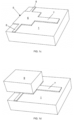
- Figure 1a shows a silicon substrate 1 wherein a pyramid-shaped mold 2 is produced. This is typically done by anisotropic wet etching along the crystallographic planes of the substrate. This is achievable for example when the substrate 1 is a (100) oriented Si substrate, by wet etching the substrate in a square opening while the rest of the substrate is protected by a mask.
- the dimensions of the mold are in the order of micrometers, for example the sides of the mold may be about 5 to 10 micrometer long and the depth of the mold may be in the same order of magnitude.
- Nano-sized diamond seed particles 3 are then deposited in the mold, as schematically illustrated in the detail image included in Figure 1a , which shows a top view of the mold.
- the seed particles enable the subsequent growth of a diamond layer in the mold.
- the deposition of the seed particles may be done by immersion seeding, wherein the substrate 1 including the mold 2 is immersed into a colloidal solution of the particles in a solvent such as ethanol or H 2 O.
- the potential of these diamond nanoparticles is adjusted to be opposite of the potential of the Si substrate which results into attraction and finally deposition of these diamond nanoparticles onto the Si surface.
- the detail image shows the particles being evenly distributed in straight arrays, but in reality the particles are distributed more randomly.
- the particles are non-doped diamond particles.
- the density of the particles when deposited in the mold may be in accordance with existing methods, for example between 1E10/cm 2 and 5E10/cm 2 .
- the density may however be controlled within a larger range of 1E9/cm 2 and 1E11/cm 2 by adjusting the seeding dispersion chemistry, the particle and substrate potential and the seeding time.
- the applied density must be such that it enables the growth of a closed (i.e. fully coalesced) diamond layer in the mold.
- the particles consist of a mixture of non-doped diamond particles and doped diamond particles, deposited at any of the above-described densities.
- Both the doped and non-doped particles enable the growth of a closed diamond layer, but only the non-doped particles will act later on as masks for the creation of the nano-tips in accordance with the invention.
- the diameter of the individual particles is typically 3 to 5 nm but they often cluster to aggregates leading to a size distribution of typically 5 to 25 nm.
- a doped diamond layer is then deposited for example by chemical vapour deposition (CVD).
- the dopant may be boron.
- the diamond layer is deposited in the mold 2 and on the surface of the substrate 1, after which it is patterned to form a patch 4 of the diamond layer inside and around the mold, as shown in Figure 1b .
- the cavity of the mold is thus not fully filled with diamond, but a layer of diamond is deposited on the inverted pyramid surfaces of the mold.
- the thickness of the diamond layer may vary according to the required probe characteristics. Diamond layers of about 1 micrometer thick are often used, but thinner layers are possible, for example about 100nm. It is also possible to produce a full diamond tip by filling the entire mold with diamond.
- the diamond deposition is followed by the deposition and patterning of a metal layer stack 5 as illustrated in Figure 1c .
- a metal layer stack 5 as illustrated in Figure 1c .
- This may for example be a combination of TaN (about 50nm) acting as adhesion and peel-off layer, Cu (about 50 nm) as seed layer for Ni electroplating, and Ni as cantilever material (about 5 microns).
- the metal fills the remainder of the mold cavity, so that this cavity is eventually filled by a solid tip formed of a metal core with a diamond layer on it.
- the patterning of the metal is done so that a base portion 6 is formed, with a cantilever 7 extending outward from the base portion 6.
- the distal end of the cantilever covers the diamond patch 4.
- Lateral arms 8 which extend outward on both sides of the base portion 6 may be included for facilitating the release of the probe.
- the cantilever 7 and the tip inside the mold are subsequently underetched and the base portion 6 is slightly peeled away from the substrate, overcoming the adhesion of the peel-off layer.
- a silicon holder chip 9 is then attached to the base portion 6, as shown in Figure 1d , and the assembly is taken away from the substrate, resulting in the finished probe shown in Figure 1e .
- a pyramid-shaped tip body 10 having a Ni core and a diamond layer at the exterior of the pyramid and at the tip, with a ground plane 11 also formed of diamond and extending around the tip body 10.
- the ground plane 11 is embedded in the material of the cantilever 7.
- the method step that characterizes this embodiment of the method of the invention is a step that is added to the above-described fabrication.
- the probe as shown in Figure 1e is subjected to a plasma etch procedure.
- This may be Reactive Ion Etching (RIE) or Inductive Coupled Plasma (ICP) etching, configured so that the non-doped diamond nanoparticles 3 have a lower etch rate than the doped diamond of the tip body 10.
- RIE Reactive Ion Etching
- ICP Inductive Coupled Plasma
- a suitable etch process having this effect is a plasma etch using O 2 as the plasma gas, hereafter referred to as O 2 -plasma, and well known in the art (an example of suitable parameters is given further in this description).
- O 2 -plasma a plasma etch using O 2 as the plasma gas
- a thin (typically 1-5 nm thick) silicon oxycarbide layer is spontaneously formed with a non-uniform thickness.
- Silicon oxycarbide is the compound SiO x C y , with x ⁇ 2 and y>0.
- the SiO x C y layer is etched slower by an O 2 plasma etch than the doped diamond, i.e. the SiO x C y also acts as an etch mask.
- the SiO x C y layer 12 is formed on the mold surface 13, in the spaces between adjacent seed particles 3, and grows thicker until the space in between the growing doped diamond islands 14 is closed and a fully coalesced diamond film 4 is formed.
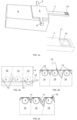
- the outer surface of the probe after its release from the mold is shown in Figure 2b .
- the SiOxCy layer 12 together with the nanoparticles 3 form a layer 16 of irregular thickness, visualized by the bold lines in Figure 2b .
- this tip is subjected to O 2 -plasma etching, the SiO x C y portions 12 and the nanoparticles 3 are slowly etched away, until parts of the doped diamond layer 4 become exposed. This happens locally due to the irregularity of the thickness of layer 16.
- nanotips are formed in the diamond layer 4, resulting in a 'hedgehog' tip structure illustrated in Figure 3a .
- the nanotips 15 are distributed on the totality of the pyramid-shaped tip body 10 and on the diamond ground plane 11 around the tip body.
- the tip is first subjected to a short plasma etch using SF 6 or a mixture of SF 6 and O 2 as the plasma gas, for example for about 20 s.
- This short 'flash' etch creates craters 17 in the SiO x C y layer 12, as illustrated in Figure 2c .
- This step is followed by an O 2 plasma etch as described above.
- the prior removal of a portion of the SiO x C y leads to a quicker exposure of the doped diamond layer 4, so that the 'hedgehog' structure of Figure 3a is obtained in an overall shorter timespan.
- a third masking effect may occur during the plasma etch procedure itself.
- the energy of the plasma may release particles from materials inside the etch chamber and/or from the cantilever by sputtering, wherein said particles are deposited on the tip where they can also act as an etch mask for a given etch recipe.
- polymeric etch residues deposited on the tip during the etch process may have the masking effect.
- the sputtering of Ni particles from the cantilever may become an important contributor to the formation of the nanotips 15.
- Ni-particles are released from the cantilever by sputtering under the influence of the ion bombardment generated by O 2 , SF 6 or SF 6 /O plasma. Also because of the bombardment with ions from the plasma, the pyramid gains static charge, resulting in an electric field, which attracts the Ni-particles. The Ni-particles are thereby deposited on the pyramid, but Ni is essentially not etched by SF 6 nor by O 2 plasma, so that the Ni-particles are also acting as etch masks in the same way as the seed particles 3 and SiO x C y layer portions 12. The field is stronger where the surface is sharper, i.e.
- the concentration of Ni-particles is higher in these areas, which may be exploited for the production of specific tip structures (see further).
- the SiO x C y 12 the seed particles 3 and the Ni-particles have the combined effect of producing the 'hedgehog' structure illustrated in Figure 3a .
- the SiO x C y and seed particle effects are more important at the start of the etch process, and may be the dominant processes in the case of thin diamond layers, e.g. about 100nm. For thicker diamond layers, e.g. 1 micrometer, or full diamond tips, all three effects contribute to the formation of the nanotips 15 and the Ni-sputtering effect will become dominant after the SiO x C y and the seed particles have been etched away.
- all three masking effects may contribute to the formation of the 'hedgehog' structure in the case of diamond tip produced in a Si mold on a Ni cantilever.
- any one of the above masking effects may occur alone or in combination with the others.
- the cantilever material is not a suitable etch mask, the sputtering effect is not or less relevant. It is also possible that a layer similar to the SiO x C y is not formed, or does not have a masking effect. The presence of seed particles in a mold is not always required, as is the case for a TiN probe tip, see further.
- the 'mask layer' referred to in appended claim 1 may consist of various constituent parts. It comprises a layer of irregular thickness, like layer 16 in Figure 2b , formed prior to the etch procedure.
- the masking layer may also comprise particles which contribute to the formation of this layer during the etch procedure itself.
- the ⁇ layer of irregular thickness' referred to in the appended claims may have various compositions depending on the materials and fabrication process of the probe tip. The layer could consist only of seed particles, or it could consist only of compounds formed spontaneously on the tip body, such as oxides formed on a TiN probe tip, see further.
- the layer can be closed, so that none of the probe material is initially exposed to the plasma, but this probe material only becomes exposed when the mask layer is locally etched away. This necessarily occurs locally due to the irregular thickness of the layer.
- the layer of irregular thickness may also be a layer that exposes locally the underlying probe material from the start of the etch procedure, for example a layer consisting only of seed particles, with thickness zero in between the seed particles.
- the etch procedures described above are stopped when the nanotips 15 have obtained a given shape and aspect ratio.
- the O 2 -etch duration defines the shape of the nanotips.
- the nanotips are cone-shaped pillars, as illustrated in Figure 3a .
- the etch time can thus be controlled to obtain a given shape.
- portions of the seed particles and/or the SiO x C y layer and/or of the sputtered particles may still be present on the nanotips.
- these remnants of the etch mask are not a problem and they may remain. Otherwise, a slight oxygen overetch may burn away these remnants, or when the tip is used in an electrical SPM measurement, the remnant may be removed by briefly applying a high bias voltage or a high scanning force.
- the drawing in Figure 3a is a schematic representation.
- the number of nanotips 15 may be higher and the nanotips may be distributed more randomly across the diamond surface.
- the dimensions of the nanotips are in the order of nanometers, for example a height of about 50 to 100nm.
- the radius of the apex area of the nanotips ranges from less than 1 nm up to a few nanometer, which is comparable to or better than the radius of a standard pyramid-shaped tip, but the nanotips are considerably smaller and more pointed than the tip body 10 prior to the etch procedure.
- the aspect ratio of the nanotips 15 is much higher compared to the aspect ratio of the apex area of the tip body 10 prior to the etch procedure.
- the aspect ratio of the apex area may be determined by approximating the apex area as a spherical surface and determining the aspect ratio as the ratio of the average diameter of the surface to its height.
- the aspect ratio of the nanotips may be calculated according to generally established definitions in accordance with the shape of the nanotips, for example as the ratio of the average width of a cone-shaped tip to the height of the tip.
- the method of the invention thus provides a way to produce a probe with increased aspect ratio of the tip portion that is actually in contact with the surface, and without requiring complex micromachining or other fabrication methods.
- the etch process is self-aligned, and requires no lithographic mask other than the particles, SiO x C y layer or other contributors to the mask layer referred to in appended claim 1.
- the nanotip that enters into contact with the sample may be the outermost nanotip on the top of the pyramid, or one of the tips adjacent to it, dependent on the angular position of the probe.
- This type of probe is therefore very suitable for use in combination with a tiltable SPM head, known per se in the art.
- the fact that a plurality of nanotips 15 is present, ensures that at least one of these tips contacts the sample.
- the presence of multiple sharp nanotips also makes the probe tip according to the invention suitable for scratching a surface and removing material from the surface, as applied for example in the known 'scalpel AFM' technique.
- the tip produced by the invention and comprising multiple sharp nanotips is for attaching nano/micro objects such as biological cells to the sharp nano-tips. This is enabled by the known fact that a plurality of closely spaced nano-tips are capable of influencing the wettability of a surface.
- the invention is not limited to the 'hedgehog' type structure described above.
- the dry etch process is continued until the nanotips 15 are etched away on the side planes of the pyramid.
- one or more nanotips 15 are nevertheless formed on the apex area of the tip body 10, as schematically illustrated in Figures 3b and 3c .
- This tip structure referred to hereafter as the 'tip-on-tip embodiment' may be obtained by exploiting one or more effects, possibly occurring simultaneously.
- the sputtering of Ni particles from the cantilever during the etch process is one effect that contributes to this type of tip structure.
- the electric field generated by the ion bombardment is stronger where the surface is sharper, i.e. at the pyramid plane edges and mostly at the apex.
- the field attracts the Ni particles, so there are more etch mask particles at the apex than on the sidewalls.
- the tip body is therefore entirely formed by Ni, except for the sharp diamond tips 15 in the apex area.
- a second contributor to this 'tip on tip' embodiment is the fact that the diamond layer may be thicker near the apex region compared to on the side planes of the pyramid.
- Figure 4 shows a cross-section of a diamond coated probe tip body, having a Ni core 20 and a doped diamond layer 21.
- Figure 4 also shows schematically the presence of the non-doped diamond seed particles 3 and of the SiO x C y layer 12. It is seen that the thickness of the diamond layer, as measured in the direction perpendicular to the ground plane of the pyramid, is larger at the apex region (thickness a 1 ) than on the sides of the pyramid (thickness a 2 ).
- the invention is applicable to the production of any type of probe suitable for SPM scanning, formed of any known material, for example Si and Si-compound tips or metal and metal alloy tips.
- the method is equally applicable to diamond tips other than boron-doped diamond tips, for example phosphor-doped diamond, non-doped diamond, NV (Nitrogen Vacancy) diamond.
- the inventors have produced a 'hedgehog' probe tip comprising nano-tips 15 formed of TiN on a Ni cantilever.
- the probe was fabricated by a molding technique similar to the methods described above. However instead of a diamond CVD layer, a TiN layer, about 150nm thick was deposited in the Si mold by sputtering of TiN. No seed particles were deposited in the mold.
- the layer of irregular thickness formed on the TiN is initially an oxide layer that spontaneously forms on the outer surface of the TiN pyramid, after its release from the mold.
- the oxide works as an etch mask in a plasma etch process under mixed SF 6 /O 2 atmosphere, in the same way as the combined effect of the seed particles and SiO x C y described above, i.e. the oxide is slowly etched, so that the TiN layer underneath is locally exposed and subsequently etched at a faster rate.
- sputtered Ni particles contribute to the mask layer, equally as described above. Exposure of the tip to a plasma etch under this atmosphere thereby produced the 'hedgehog' structure with TiN nanotips 15. Details of suitable etch parameters are provided further in this description.
- the invention is not limited to pyramid-shaped tips.
- the nanotips 15 may be produced on other tip geometries as well.
- Figure 5a illustrates an in-plane probe as known for example from US8484761 .
- the image shows the cantilever 7 with a diamond tip body 10 extending outward from the cantilever and lying in the plane of the cantilever.
- Figure 5b shows the same probe in a side view and a detail of the tip area, after applying an etch procedure.
- the nanotips 15 extend in the direction perpendicular to the plane of the cantilever 7 and the tip body 10.
- Particles having the above-described mask effect may be deposited in a separate deposition step, and/or if the cantilever material is suitable for this purpose, masking particles may be deposited during the etching step itself, by sputtering of the cantilever material, and/or of material inside the etch chamber, and/or by the masking effect of etch residues.
- Additional method steps may be performed after completion of the method according to any of the embodiments described above. These additional method steps include :
- the capping layer forms a sleeve around the nanotips 15, leaving the apex of the nanotips exposed, so that the function of the nanotips in an SPM apparatus or other application is not inhibited.
- the capping layer reinforces the nanotips, i.e. it increases the mechanical resistance of the nanotips, while the tips remain capable of performing their function. This embodiment is beneficial especially in high-force applications, where the capping layer helps to protect the nanotips from breaking off.
- the capping layer may be an SiO x layer (1 ⁇ x ⁇ 2) deposited on a hedgehog type probe tip as shown in Figure 3a or on a 'tip-on-tip' probe tip as shown in Figures 3b and 3c .
- the SiO x layer may be deposited by plasma-enhanced chemical vapour deposition (PECVD).
- PECVD plasma-enhanced chemical vapour deposition
- the thickness of the SiO x layer may be in the order of a few tens of nanometer, e.g. about 50 nm.
- the etch process for removing the SiO x layer from the apex area may be a plasma etch using a mixture of SF 6 and O 2 . The etch process is stopped when at least the apex of the nanotips is exposed. A more detailed description of suitable parameters is described further in this description.
- a capping layer on the one or more nanotips 15 can be applied also on a 'tip-on-tip' probe as described in the prior art, i.e. a probe tip comprising nanotips on the apex area of the tip body, but wherein the nanotips are produced by a method other than the above-described method involving the production of these nanotips by a self-aligned etch process.
- the capping layer may be produced by the same steps as described above, on a probe tip produced by the method described in document US6328902 .
- the present invention is therefore equally related to a method for producing a probe tip suitable for scanning probe microscopy (SPM), comprising the steps of :
- the disclosure equally includes a probe tip suitable for scanning probe microscopy (SPM), comprising a probe tip body having an apex area and comprising one or more tip portions on the apex area of the tip body, and no tip portions on the remainder of the tip body, the tip portions being considerably smaller and more pointed than the tip body, wherein the tip portions comprise a capping layer on their outer surface except on a tip area of the tip portions, the tip area comprising the apex of the tip portions.
- SPM scanning probe microscopy
- suitable parameters for producing a capping layer described in the following section is applicable to a diamond probe tip of the 'tip on tip' type, produced by the self-aligned etch method, by the method of US6328902 or by any other method known in the art.
- the inventors produced a diamond ⁇ full hedgehog' tip on a probe comprising a tip body produced by the above-described molding technique : Si mold, non-doped seed particles deposited in the mold (density about 1E10/cm 2 ), Ni cantilever, diamond layer (about 800nm thick) on Ni core.
- a diamond 'tip on tip' probe as shown in Figure 3c was produced on a probe tip produced by the same method, in the same ICP reactor, applying the same RF and ICP power and same chamber pressure, but by the following sequence of etch steps:
- the TiN full hedgehog tip referred to above was produced by the following etch conditions : Table 2: Plasma reactor type ICP Plasma gas Mixed SF 6 /O 2 Gas flow (of plasma gas) 40 sccm (SF 6 )/10 sccm (O 2 )* RF power 50 W ICP power 300 W Chamber pressure 10 mTorr Etch duration 5 min * the gas flow was supplied at 294K and 3atm
- a SiO x layer was deposited by PACVD, with a thickness of about 50nm.
- the tip was subsequently subjected to an SF 6 /O 2 plasma etch with the parameters shown in Table 3.
- Table 3 Plasma reactor type ICP Plasma gas Mixed SF 6 /O 2 Gas flow (of plasma gas) 2.5 sccm (SF 6 )/50 sccm (O 2 )* RF power 25 W ICP power 1200 W Chamber pressure 10 mTorr Etch duration 5 min the gas flow was supplied at 294K and 3atm.
- the result was that the SiOx layer was removed from the apex of the nanotips, while forming a reinforcing capping layer around the lateral surface of the nanotips.
Landscapes
- Chemical & Material Sciences (AREA)
- Engineering & Computer Science (AREA)
- Materials Engineering (AREA)
- Metallurgy (AREA)
- Organic Chemistry (AREA)
- General Chemical & Material Sciences (AREA)
- Chemical Kinetics & Catalysis (AREA)
- Physics & Mathematics (AREA)
- Mechanical Engineering (AREA)
- Health & Medical Sciences (AREA)
- General Health & Medical Sciences (AREA)
- General Physics & Mathematics (AREA)
- Nuclear Medicine, Radiotherapy & Molecular Imaging (AREA)
- Radiology & Medical Imaging (AREA)
- Crystallography & Structural Chemistry (AREA)
- Inorganic Chemistry (AREA)
- Plasma & Fusion (AREA)
- Micromachines (AREA)
- Length Measuring Devices With Unspecified Measuring Means (AREA)
Claims (8)
- Verfahren zur Herstellung einer für die Rastersondenmikroskopie (SPM) geeigneten Sondenspitze, umfassend die Schritte zum:- Herstellen eines Sondenspitzenkörpers (10), der mindestens eine äußere Schicht (21) aus einem Sondenmaterial umfasst, wobei der Spitzenkörper einen Scheitelbereich umfasst,- Während des Herstellungsprozesses des Sondenspitzenkörpers und/oder nach dem Herstellungsprozess Bilden einer Maskenschicht auf der äußeren Schicht aus Sondenmaterial,- Unterziehen des Sondenspitzenkörpers (10) einem Plasmaätzvorgang, wobei die Maskenschicht als eine Ätzmaske für das Ätzen des Sondenmaterials dient, und wobei der Ätzvorgang und die Ätzmaske konfiguriert sind, um einen oder mehrere Spitzenabschnitte (15) herzustellen, die aus dem Sondenmaterial gebildet sind, wobei der eine oder mehrere Spitzenabschnitte erheblich kleiner sind und ein höheres Aspektverhältnis als der Scheitelbereich des Spitzenkörpers (10) vor dem Ätzvorgang aufweisen,und wobei:- die Maskenschicht eine Schicht mit unregelmäßiger Dicke (16) umfasst, die vor dem Ätzvorgang gebildet wird, wobei die Schicht mit unregelmäßiger Dicke als Ätzmaske für das Ätzen des Sondenmaterials dient,- der Spitzenkörper (10) durch Herstellen einer Form (2) in einem Substrat (1) und durch Abscheiden des Sondenmaterials in der Form hergestellt wird, wobei:- Keimteilchen (3) in der Form (2) vor dem Abscheiden des Sondenmaterials darin abgeschieden werden, wobei die Schicht mit unregelmäßiger Dicke (16) die Keimteilchen (3) umfasst, und wobei die Keimteilchen (3) mit einer langsameren Rate als das Sondenmaterial geätzt werden, und/oder- die Schicht mit unregelmäßiger Dicke (16) Verbindungen umfasst, die sich nach dem Herstellungsprozess des Spitzenkörpers und vor dem Ätzvorgang spontan, z. B. durch Oxidation, auf der Oberfläche des Spitzenkörpers (10) bilden.
- Verfahren nach Anspruch 1, wobei die Schicht mit unregelmäßiger Dicke (16) weiter Verbindungen (12) umfasst, die sich spontan auf der Oberfläche der Form (2) bilden.
- Verfahren nach einem der Ansprüche 1 oder 2, wobei der Ätzvorgang umfasst:- Einen ersten Ätzprozess, der während einer ersten kurzen Ätzzeit durchgeführt wird und konfiguriert ist, um Krater (17) in der Schicht (16) mit unregelmäßiger Dicke herzustellen,- Einen zweiten Ätzprozess, der während einer zweiten Ätzzeit durchgeführt wird, die erheblich länger ist als die erste Ätzzeit, und konfiguriert ist, eine oder mehrere Spitzenabschnitte (15) herzustellen.
- Verfahren nach einem der vorstehenden Ansprüche, wobei der Sondenspitzenkörper (10) an einem Ausleger (7) befestigt ist und wobei Teilchen des Auslegermaterials während des Ätzvorgangs gesputtert und auf dem Sondenspitzenkörper (10) abgeschieden werden, und wobei die gesputterten Teilchen aus dem Ausleger zur Bildung der Maskenschicht während des restlichen Ätzvorgangs beitragen.
- Verfahren nach einem der vorstehenden Ansprüche, wobei am Ende des Ätzvorgangs die Spitzenabschnitte (15) über die Gesamtheit des Spitzenkörpers (10) verteilt sind.
- Verfahren nach einem der Ansprüche 1 bis 4, wobei der Spitzenkörper (10) pyramidenförmig ist und wobei am Ende des Ätzvorgangs ein oder mehrere Spitzenabschnitte (15) im Scheitelbereich des Spitzenkörpers vorhanden sind und keine Spitzenabschnitte in den Seitenebenen des Spitzenkörpers vorhanden sind, durch einen oder eine Kombination der folgenden Effekte:- während des Ätzvorgangs wird im Scheitelbereich eine höhere Konzentration von Maskierungsteilchen abgeschieden als auf den Seitenebenen,- der Spitzenkörper (10) umfasst einen Kern (20) und auf dem Kern eine Schicht (21) aus dem Sondenmaterial, und die Dicke der Schicht ist im Scheitelbereich größer als in den Seitenebenen, sodass am Ende des Ätzvorgangs das Sondenmaterial von den Seitenebenen entfernt ist.
- Verfahren nach einem der vorstehenden Ansprüche, wobei das Sondenmaterial Diamant ist.
- Verfahren nach einem der vorstehenden Ansprüche, das weiter die folgenden Schritte umfasst, die nach dem Ätzvorgang durchgeführt werden:- Abscheiden einer Abdeckschicht auf dem einen oder mehreren Spitzenabschnitten(15), wodurch der Spitzenabschnitt oder -abschnitte vollständig bedeckt werden,- Unterziehen der Spitzenabschnitte (15) einem Plasmaätzprozess, der konfiguriert ist, um den Abdeckschicht von einem Spitzenbereich des einen oder mehrerer Spitzenabschnitte zu entfernen, wobei der Spitzenbereich den Scheitel des einen oder mehrerer Spitzenabschnitte beinhaltet, während die Abdeckschicht um die Seitenoberfläche des einen oder mehrerer Spitzenabschnitte (15) herum im Wesentlichen erhalten bleibt.
Priority Applications (3)
| Application Number | Priority Date | Filing Date | Title |
|---|---|---|---|
| EP19160202.8A EP3702792B1 (de) | 2019-03-01 | 2019-03-01 | Verfahren zur herstellung einer sonde für die rastersondenmikroskopie |
| US16/802,944 US11035880B2 (en) | 2019-03-01 | 2020-02-27 | Method for producing a probe suitable for scanning probe microscopy |
| JP2020031411A JP7553247B2 (ja) | 2019-03-01 | 2020-02-27 | 走査型プローブ顕微鏡に適したプローブの製造方法 |
Applications Claiming Priority (1)
| Application Number | Priority Date | Filing Date | Title |
|---|---|---|---|
| EP19160202.8A EP3702792B1 (de) | 2019-03-01 | 2019-03-01 | Verfahren zur herstellung einer sonde für die rastersondenmikroskopie |
Publications (2)
| Publication Number | Publication Date |
|---|---|
| EP3702792A1 EP3702792A1 (de) | 2020-09-02 |
| EP3702792B1 true EP3702792B1 (de) | 2025-02-12 |
Family
ID=65657329
Family Applications (1)
| Application Number | Title | Priority Date | Filing Date |
|---|---|---|---|
| EP19160202.8A Active EP3702792B1 (de) | 2019-03-01 | 2019-03-01 | Verfahren zur herstellung einer sonde für die rastersondenmikroskopie |
Country Status (3)
| Country | Link |
|---|---|
| US (1) | US11035880B2 (de) |
| EP (1) | EP3702792B1 (de) |
| JP (1) | JP7553247B2 (de) |
Family Cites Families (13)
| Publication number | Priority date | Publication date | Assignee | Title |
|---|---|---|---|---|
| JPH0275902A (ja) * | 1988-09-13 | 1990-03-15 | Seiko Instr Inc | ダイヤモンド探針及びその成形方法 |
| US5221415A (en) | 1989-01-17 | 1993-06-22 | Board Of Trustees Of The Leland Stanford Junior University | Method of forming microfabricated cantilever stylus with integrated pyramidal tip |
| US5611942A (en) * | 1995-03-02 | 1997-03-18 | Kabushiki Kaisha Toshiba | Method for producing tips for atomic force microscopes |
| JP3805418B2 (ja) * | 1995-12-25 | 2006-08-02 | オリンパス株式会社 | Afmカンチレバー |
| EP0927331B1 (de) * | 1996-08-08 | 2004-03-31 | William Marsh Rice University | Makroskopisch manipulierbare, aus nanoröhrenanordnungen hergestellte vorrichtungen |
| EP0899538B1 (de) | 1997-08-27 | 2003-05-14 | IMEC vzw | Taststift-Konfiguration sowie Herstellungsverfahren und Verwendung von Taststiften |
| JP4733319B2 (ja) | 2000-09-18 | 2011-07-27 | アイメック | プローブチップ構造の製造方法 |
| JP4688400B2 (ja) * | 2001-12-04 | 2011-05-25 | エスアイアイ・ナノテクノロジー株式会社 | 走査型プローブ顕微鏡用探針 |
| US7370515B2 (en) * | 2004-06-21 | 2008-05-13 | Veeco Instruments Inc. | Probes for use in scanning probe microscopes and methods of fabricating such probes |
| WO2009012180A1 (en) * | 2007-07-13 | 2009-01-22 | Advanced Diamond Technologies, Inc. | Ultrananocrystalline diamond film deposition for spm probes |
| JP5889510B2 (ja) | 2008-06-11 | 2016-03-22 | アイメックImec | 原子間力顕微鏡プローブ構成の製造方法 |
| DE102010035931A1 (de) * | 2010-08-31 | 2012-03-01 | Fraunhofer-Gesellschaft zur Förderung der angewandten Forschung e.V. | Verfahren zur Herstellung einer Messspitze für ein Rastersondenmikroskop sowie Messsonde mit nach diesem Verfahren hergestellter Messspitze |
| EP2458391A1 (de) * | 2010-11-29 | 2012-05-30 | Technische Universität Wien | AFM-SECM-Sensor |
-
2019
- 2019-03-01 EP EP19160202.8A patent/EP3702792B1/de active Active
-
2020
- 2020-02-27 US US16/802,944 patent/US11035880B2/en active Active
- 2020-02-27 JP JP2020031411A patent/JP7553247B2/ja active Active
Also Published As
| Publication number | Publication date |
|---|---|
| EP3702792A1 (de) | 2020-09-02 |
| JP2020144120A (ja) | 2020-09-10 |
| JP7553247B2 (ja) | 2024-09-18 |
| US11035880B2 (en) | 2021-06-15 |
| US20200278379A1 (en) | 2020-09-03 |
Similar Documents
| Publication | Publication Date | Title |
|---|---|---|
| US6864481B2 (en) | Probe for scanning probe microscope | |
| US6914008B2 (en) | Structure having pores and its manufacturing method | |
| EP2231507B1 (de) | Verfahren zur herstellung einer 3d-nanostruktur mit einer nanosubstruktur, wie eine isolierpyramide mit einer metallspitze | |
| Fasching et al. | Cantilever tip probe arrays for simultaneous SECM and AFM analysis | |
| WO2006041691A2 (en) | Improved nanotube-based nanoprobe structure and method for making the same | |
| TWI229050B (en) | Microstructures | |
| CN110658360B (zh) | 一种超细原子力显微镜金属探针的制备方法和装置 | |
| US8168251B2 (en) | Method for producing tapered metallic nanowire tips on atomic force microscope cantilevers | |
| EP3702792B1 (de) | Verfahren zur herstellung einer sonde für die rastersondenmikroskopie | |
| WO2004102582A1 (en) | Carbon nanotube-based probes, related devices and methods of forming the same | |
| DE69817452T2 (de) | Verfahren zur Herstellung einer micromechanischen Messsonde, insbesondere eines Rasterkraftmikroskops | |
| US11955368B2 (en) | Wafer configured to recondition a support surface of a wafer holding stage | |
| US6227519B1 (en) | Female mold substrate having a heat flowable layer, method to make the same, and method to make a microprobe tip using the female substrate | |
| TWI439696B (zh) | Probe tip modification method | |
| JP4858924B2 (ja) | 走査型プローブ顕微鏡用探針の作成方法 | |
| EP2835654A1 (de) | Isolatorbeschichtete leitfähige Sonde und Verfahren zu deren Herstellung | |
| EP4379397A1 (de) | Verfahren zur herstellung eines substrats mit mehreren spitzen für die rastersondenmikroskopie | |
| Tao et al. | Ultrasharp high-aspect-ratio probe array for SECM and AFM Analysis | |
| WO2012028314A1 (de) | Verfahren zur herstellung einer messspitze für ein rastersondenmikroskop sowie messsonde mit nach diesem verfahren hergestellter messspitze | |
| Bajikar et al. | Microfabrication of extraction electrodes for local-electrode atom probes | |
| Chen et al. | Electrochemical preparation of STM probes for high aspect ratio nanometrology | |
| Moening | Formation of nano-sharp tips and microbumps on silicon and metal films by localized single-pulse laser irradiation | |
| Vorob'eva | Anodic-Oxidation Growth of Microscopic Pillar Arrays: Kinetic Aspects | |
| Friesen et al. | Nanoscale mechanical patterning for the selective deposition of nanostructures | |
| Beuret | Development of a double molding technique for the microfabrication of diamond scanning probe tips |
Legal Events
| Date | Code | Title | Description |
|---|---|---|---|
| PUAI | Public reference made under article 153(3) epc to a published international application that has entered the european phase |
Free format text: ORIGINAL CODE: 0009012 |
|
| STAA | Information on the status of an ep patent application or granted ep patent |
Free format text: STATUS: THE APPLICATION HAS BEEN PUBLISHED |
|
| AK | Designated contracting states |
Kind code of ref document: A1 Designated state(s): AL AT BE BG CH CY CZ DE DK EE ES FI FR GB GR HR HU IE IS IT LI LT LU LV MC MK MT NL NO PL PT RO RS SE SI SK SM TR |
|
| AX | Request for extension of the european patent |
Extension state: BA ME |
|
| STAA | Information on the status of an ep patent application or granted ep patent |
Free format text: STATUS: REQUEST FOR EXAMINATION WAS MADE |
|
| 17P | Request for examination filed |
Effective date: 20210224 |
|
| RBV | Designated contracting states (corrected) |
Designated state(s): AL AT BE BG CH CY CZ DE DK EE ES FI FR GB GR HR HU IE IS IT LI LT LU LV MC MK MT NL NO PL PT RO RS SE SI SK SM TR |
|
| STAA | Information on the status of an ep patent application or granted ep patent |
Free format text: STATUS: EXAMINATION IS IN PROGRESS |
|
| 17Q | First examination report despatched |
Effective date: 20220523 |
|
| GRAP | Despatch of communication of intention to grant a patent |
Free format text: ORIGINAL CODE: EPIDOSNIGR1 |
|
| STAA | Information on the status of an ep patent application or granted ep patent |
Free format text: STATUS: GRANT OF PATENT IS INTENDED |
|
| INTG | Intention to grant announced |
Effective date: 20240909 |
|
| P01 | Opt-out of the competence of the unified patent court (upc) registered |
Free format text: CASE NUMBER: APP_58998/2024 Effective date: 20241029 |
|
| GRAS | Grant fee paid |
Free format text: ORIGINAL CODE: EPIDOSNIGR3 |
|
| GRAA | (expected) grant |
Free format text: ORIGINAL CODE: 0009210 |
|
| STAA | Information on the status of an ep patent application or granted ep patent |
Free format text: STATUS: THE PATENT HAS BEEN GRANTED |
|
| AK | Designated contracting states |
Kind code of ref document: B1 Designated state(s): AL AT BE BG CH CY CZ DE DK EE ES FI FR GB GR HR HU IE IS IT LI LT LU LV MC MK MT NL NO PL PT RO RS SE SI SK SM TR |
|
| REG | Reference to a national code |
Ref country code: GB Ref legal event code: FG4D |
|
| REG | Reference to a national code |
Ref country code: CH Ref legal event code: EP |
|
| REG | Reference to a national code |
Ref country code: DE Ref legal event code: R096 Ref document number: 602019065677 Country of ref document: DE |
|
| REG | Reference to a national code |
Ref country code: IE Ref legal event code: FG4D |
|
| PGFP | Annual fee paid to national office [announced via postgrant information from national office to epo] |
Ref country code: DE Payment date: 20250319 Year of fee payment: 7 |
|
| REG | Reference to a national code |
Ref country code: NL Ref legal event code: MP Effective date: 20250212 |
|
| PG25 | Lapsed in a contracting state [announced via postgrant information from national office to epo] |
Ref country code: RS Free format text: LAPSE BECAUSE OF FAILURE TO SUBMIT A TRANSLATION OF THE DESCRIPTION OR TO PAY THE FEE WITHIN THE PRESCRIBED TIME-LIMIT Effective date: 20250512 |
|
| PG25 | Lapsed in a contracting state [announced via postgrant information from national office to epo] |
Ref country code: FI Free format text: LAPSE BECAUSE OF FAILURE TO SUBMIT A TRANSLATION OF THE DESCRIPTION OR TO PAY THE FEE WITHIN THE PRESCRIBED TIME-LIMIT Effective date: 20250212 |
|
| PG25 | Lapsed in a contracting state [announced via postgrant information from national office to epo] |
Ref country code: PL Free format text: LAPSE BECAUSE OF FAILURE TO SUBMIT A TRANSLATION OF THE DESCRIPTION OR TO PAY THE FEE WITHIN THE PRESCRIBED TIME-LIMIT Effective date: 20250212 |
|
| PG25 | Lapsed in a contracting state [announced via postgrant information from national office to epo] |
Ref country code: ES Free format text: LAPSE BECAUSE OF FAILURE TO SUBMIT A TRANSLATION OF THE DESCRIPTION OR TO PAY THE FEE WITHIN THE PRESCRIBED TIME-LIMIT Effective date: 20250212 |
|
| REG | Reference to a national code |
Ref country code: LT Ref legal event code: MG9D |
|
| PG25 | Lapsed in a contracting state [announced via postgrant information from national office to epo] |
Ref country code: IS Free format text: LAPSE BECAUSE OF FAILURE TO SUBMIT A TRANSLATION OF THE DESCRIPTION OR TO PAY THE FEE WITHIN THE PRESCRIBED TIME-LIMIT Effective date: 20250612 Ref country code: NO Free format text: LAPSE BECAUSE OF FAILURE TO SUBMIT A TRANSLATION OF THE DESCRIPTION OR TO PAY THE FEE WITHIN THE PRESCRIBED TIME-LIMIT Effective date: 20250512 |
|
| PG25 | Lapsed in a contracting state [announced via postgrant information from national office to epo] |
Ref country code: NL Free format text: LAPSE BECAUSE OF FAILURE TO SUBMIT A TRANSLATION OF THE DESCRIPTION OR TO PAY THE FEE WITHIN THE PRESCRIBED TIME-LIMIT Effective date: 20250212 |
|
| PG25 | Lapsed in a contracting state [announced via postgrant information from national office to epo] |
Ref country code: HR Free format text: LAPSE BECAUSE OF FAILURE TO SUBMIT A TRANSLATION OF THE DESCRIPTION OR TO PAY THE FEE WITHIN THE PRESCRIBED TIME-LIMIT Effective date: 20250212 |
|
| PG25 | Lapsed in a contracting state [announced via postgrant information from national office to epo] |
Ref country code: LV Free format text: LAPSE BECAUSE OF FAILURE TO SUBMIT A TRANSLATION OF THE DESCRIPTION OR TO PAY THE FEE WITHIN THE PRESCRIBED TIME-LIMIT Effective date: 20250212 Ref country code: PT Free format text: LAPSE BECAUSE OF FAILURE TO SUBMIT A TRANSLATION OF THE DESCRIPTION OR TO PAY THE FEE WITHIN THE PRESCRIBED TIME-LIMIT Effective date: 20250612 |
|
| PG25 | Lapsed in a contracting state [announced via postgrant information from national office to epo] |
Ref country code: BG Free format text: LAPSE BECAUSE OF FAILURE TO SUBMIT A TRANSLATION OF THE DESCRIPTION OR TO PAY THE FEE WITHIN THE PRESCRIBED TIME-LIMIT Effective date: 20250212 Ref country code: GR Free format text: LAPSE BECAUSE OF FAILURE TO SUBMIT A TRANSLATION OF THE DESCRIPTION OR TO PAY THE FEE WITHIN THE PRESCRIBED TIME-LIMIT Effective date: 20250513 |
|
| REG | Reference to a national code |
Ref country code: AT Ref legal event code: MK05 Ref document number: 1766493 Country of ref document: AT Kind code of ref document: T Effective date: 20250212 |
|
| PG25 | Lapsed in a contracting state [announced via postgrant information from national office to epo] |
Ref country code: SE Free format text: LAPSE BECAUSE OF FAILURE TO SUBMIT A TRANSLATION OF THE DESCRIPTION OR TO PAY THE FEE WITHIN THE PRESCRIBED TIME-LIMIT Effective date: 20250212 |
|
| PG25 | Lapsed in a contracting state [announced via postgrant information from national office to epo] |
Ref country code: SM Free format text: LAPSE BECAUSE OF FAILURE TO SUBMIT A TRANSLATION OF THE DESCRIPTION OR TO PAY THE FEE WITHIN THE PRESCRIBED TIME-LIMIT Effective date: 20250212 |
|
| PG25 | Lapsed in a contracting state [announced via postgrant information from national office to epo] |
Ref country code: DK Free format text: LAPSE BECAUSE OF FAILURE TO SUBMIT A TRANSLATION OF THE DESCRIPTION OR TO PAY THE FEE WITHIN THE PRESCRIBED TIME-LIMIT Effective date: 20250212 |
|
| PG25 | Lapsed in a contracting state [announced via postgrant information from national office to epo] |
Ref country code: IT Free format text: LAPSE BECAUSE OF FAILURE TO SUBMIT A TRANSLATION OF THE DESCRIPTION OR TO PAY THE FEE WITHIN THE PRESCRIBED TIME-LIMIT Effective date: 20250212 |
|
| PG25 | Lapsed in a contracting state [announced via postgrant information from national office to epo] |
Ref country code: AT Free format text: LAPSE BECAUSE OF FAILURE TO SUBMIT A TRANSLATION OF THE DESCRIPTION OR TO PAY THE FEE WITHIN THE PRESCRIBED TIME-LIMIT Effective date: 20250212 |
|
| PG25 | Lapsed in a contracting state [announced via postgrant information from national office to epo] |
Ref country code: CZ Free format text: LAPSE BECAUSE OF FAILURE TO SUBMIT A TRANSLATION OF THE DESCRIPTION OR TO PAY THE FEE WITHIN THE PRESCRIBED TIME-LIMIT Effective date: 20250212 Ref country code: EE Free format text: LAPSE BECAUSE OF FAILURE TO SUBMIT A TRANSLATION OF THE DESCRIPTION OR TO PAY THE FEE WITHIN THE PRESCRIBED TIME-LIMIT Effective date: 20250212 |
|
| PG25 | Lapsed in a contracting state [announced via postgrant information from national office to epo] |
Ref country code: RO Free format text: LAPSE BECAUSE OF FAILURE TO SUBMIT A TRANSLATION OF THE DESCRIPTION OR TO PAY THE FEE WITHIN THE PRESCRIBED TIME-LIMIT Effective date: 20250212 |
|
| REG | Reference to a national code |
Ref country code: CH Ref legal event code: H13 Free format text: ST27 STATUS EVENT CODE: U-0-0-H10-H13 (AS PROVIDED BY THE NATIONAL OFFICE) Effective date: 20251024 |
|
| PG25 | Lapsed in a contracting state [announced via postgrant information from national office to epo] |
Ref country code: SK Free format text: LAPSE BECAUSE OF FAILURE TO SUBMIT A TRANSLATION OF THE DESCRIPTION OR TO PAY THE FEE WITHIN THE PRESCRIBED TIME-LIMIT Effective date: 20250212 |
|
| REG | Reference to a national code |
Ref country code: DE Ref legal event code: R097 Ref document number: 602019065677 Country of ref document: DE |
|
| PG25 | Lapsed in a contracting state [announced via postgrant information from national office to epo] |
Ref country code: LU Free format text: LAPSE BECAUSE OF NON-PAYMENT OF DUE FEES Effective date: 20250301 |
|
| REG | Reference to a national code |
Ref country code: BE Ref legal event code: MM Effective date: 20250331 |
|
| PLBE | No opposition filed within time limit |
Free format text: ORIGINAL CODE: 0009261 |
|
| STAA | Information on the status of an ep patent application or granted ep patent |
Free format text: STATUS: NO OPPOSITION FILED WITHIN TIME LIMIT |
|
| PG25 | Lapsed in a contracting state [announced via postgrant information from national office to epo] |
Ref country code: MC Free format text: LAPSE BECAUSE OF FAILURE TO SUBMIT A TRANSLATION OF THE DESCRIPTION OR TO PAY THE FEE WITHIN THE PRESCRIBED TIME-LIMIT Effective date: 20250212 |
|
| PG25 | Lapsed in a contracting state [announced via postgrant information from national office to epo] |
Ref country code: FR Free format text: LAPSE BECAUSE OF NON-PAYMENT OF DUE FEES Effective date: 20250412 |
|
| PG25 | Lapsed in a contracting state [announced via postgrant information from national office to epo] |
Ref country code: BE Free format text: LAPSE BECAUSE OF NON-PAYMENT OF DUE FEES Effective date: 20250331 |
|
| PG25 | Lapsed in a contracting state [announced via postgrant information from national office to epo] |
Ref country code: CH Free format text: LAPSE BECAUSE OF NON-PAYMENT OF DUE FEES Effective date: 20250331 |
|
| PG25 | Lapsed in a contracting state [announced via postgrant information from national office to epo] |
Ref country code: IE Free format text: LAPSE BECAUSE OF NON-PAYMENT OF DUE FEES Effective date: 20250301 |
|
| 26N | No opposition filed |
Effective date: 20251113 |
|
| GBPC | Gb: european patent ceased through non-payment of renewal fee |
Effective date: 20250512 |