EP3688796B1 - Fabrication of apparatus including superconducting wiring layers and interconnects - Google Patents
Fabrication of apparatus including superconducting wiring layers and interconnects Download PDFInfo
- Publication number
- EP3688796B1 EP3688796B1 EP18749196.4A EP18749196A EP3688796B1 EP 3688796 B1 EP3688796 B1 EP 3688796B1 EP 18749196 A EP18749196 A EP 18749196A EP 3688796 B1 EP3688796 B1 EP 3688796B1
- Authority
- EP
- European Patent Office
- Prior art keywords
- superconducting
- layer
- niobium
- temperature
- traces
- Prior art date
- Legal status (The legal status is an assumption and is not a legal conclusion. Google has not performed a legal analysis and makes no representation as to the accuracy of the status listed.)
- Active
Links
Images



Classifications
-
- H—ELECTRICITY
- H10—SEMICONDUCTOR DEVICES; ELECTRIC SOLID-STATE DEVICES NOT OTHERWISE PROVIDED FOR
- H10N—ELECTRIC SOLID-STATE DEVICES NOT OTHERWISE PROVIDED FOR
- H10N60/00—Superconducting devices
- H10N60/01—Manufacture or treatment
- H10N60/0268—Manufacture or treatment of devices comprising copper oxide
- H10N60/0661—Processes performed after copper oxide formation, e.g. patterning
- H10N60/0688—Etching
-
- H—ELECTRICITY
- H10—SEMICONDUCTOR DEVICES; ELECTRIC SOLID-STATE DEVICES NOT OTHERWISE PROVIDED FOR
- H10N—ELECTRIC SOLID-STATE DEVICES NOT OTHERWISE PROVIDED FOR
- H10N60/00—Superconducting devices
- H10N60/01—Manufacture or treatment
- H10N60/0156—Manufacture or treatment of devices comprising Nb or an alloy of Nb with one or more of the elements of group IVB, e.g. titanium, zirconium or hafnium
-
- H—ELECTRICITY
- H10—SEMICONDUCTOR DEVICES; ELECTRIC SOLID-STATE DEVICES NOT OTHERWISE PROVIDED FOR
- H10N—ELECTRIC SOLID-STATE DEVICES NOT OTHERWISE PROVIDED FOR
- H10N60/00—Superconducting devices
- H10N60/01—Manufacture or treatment
- H10N60/0856—Manufacture or treatment of devices comprising metal borides, e.g. MgB2
-
- H—ELECTRICITY
- H10—SEMICONDUCTOR DEVICES; ELECTRIC SOLID-STATE DEVICES NOT OTHERWISE PROVIDED FOR
- H10N—ELECTRIC SOLID-STATE DEVICES NOT OTHERWISE PROVIDED FOR
- H10N60/00—Superconducting devices
- H10N60/80—Constructional details
- H10N60/805—Constructional details for Josephson-effect devices
-
- H—ELECTRICITY
- H10—SEMICONDUCTOR DEVICES; ELECTRIC SOLID-STATE DEVICES NOT OTHERWISE PROVIDED FOR
- H10N—ELECTRIC SOLID-STATE DEVICES NOT OTHERWISE PROVIDED FOR
- H10N60/00—Superconducting devices
- H10N60/80—Constructional details
- H10N60/85—Superconducting active materials
- H10N60/855—Ceramic superconductors
- H10N60/857—Ceramic superconductors comprising copper oxide
- H10N60/858—Ceramic superconductors comprising copper oxide having multilayered structures, e.g. superlattices
-
- H—ELECTRICITY
- H10—SEMICONDUCTOR DEVICES; ELECTRIC SOLID-STATE DEVICES NOT OTHERWISE PROVIDED FOR
- H10W—GENERIC PACKAGES, INTERCONNECTIONS, CONNECTORS OR OTHER CONSTRUCTIONAL DETAILS OF DEVICES COVERED BY CLASS H10
- H10W20/00—Interconnections in chips, wafers or substrates
- H10W20/01—Manufacture or treatment
- H10W20/031—Manufacture or treatment of conductive parts of the interconnections
- H10W20/064—Manufacture or treatment of conductive parts of the interconnections by modifying the conductivity of conductive parts, e.g. by alloying
-
- H—ELECTRICITY
- H10—SEMICONDUCTOR DEVICES; ELECTRIC SOLID-STATE DEVICES NOT OTHERWISE PROVIDED FOR
- H10W—GENERIC PACKAGES, INTERCONNECTIONS, CONNECTORS OR OTHER CONSTRUCTIONAL DETAILS OF DEVICES COVERED BY CLASS H10
- H10W20/00—Interconnections in chips, wafers or substrates
- H10W20/01—Manufacture or treatment
- H10W20/071—Manufacture or treatment of dielectric parts thereof
- H10W20/093—Manufacture or treatment of dielectric parts thereof by modifying materials of the dielectric parts
- H10W20/097—Manufacture or treatment of dielectric parts thereof by modifying materials of the dielectric parts by thermally treating
-
- H—ELECTRICITY
- H10—SEMICONDUCTOR DEVICES; ELECTRIC SOLID-STATE DEVICES NOT OTHERWISE PROVIDED FOR
- H10W—GENERIC PACKAGES, INTERCONNECTIONS, CONNECTORS OR OTHER CONSTRUCTIONAL DETAILS OF DEVICES COVERED BY CLASS H10
- H10W20/00—Interconnections in chips, wafers or substrates
- H10W20/40—Interconnections external to wafers or substrates, e.g. back-end-of-line [BEOL] metallisations or vias connecting to gate electrodes
- H10W20/41—Interconnections external to wafers or substrates, e.g. back-end-of-line [BEOL] metallisations or vias connecting to gate electrodes characterised by their conductive parts
- H10W20/44—Conductive materials thereof
- H10W20/4403—Conductive materials thereof based on metals, e.g. alloys, metal silicides
- H10W20/4437—Conductive materials thereof based on metals, e.g. alloys, metal silicides the principal metal being a transition metal
-
- H—ELECTRICITY
- H10—SEMICONDUCTOR DEVICES; ELECTRIC SOLID-STATE DEVICES NOT OTHERWISE PROVIDED FOR
- H10W—GENERIC PACKAGES, INTERCONNECTIONS, CONNECTORS OR OTHER CONSTRUCTIONAL DETAILS OF DEVICES COVERED BY CLASS H10
- H10W20/00—Interconnections in chips, wafers or substrates
- H10W20/40—Interconnections external to wafers or substrates, e.g. back-end-of-line [BEOL] metallisations or vias connecting to gate electrodes
- H10W20/41—Interconnections external to wafers or substrates, e.g. back-end-of-line [BEOL] metallisations or vias connecting to gate electrodes characterised by their conductive parts
- H10W20/44—Conductive materials thereof
- H10W20/4484—Superconducting materials
-
- H—ELECTRICITY
- H10—SEMICONDUCTOR DEVICES; ELECTRIC SOLID-STATE DEVICES NOT OTHERWISE PROVIDED FOR
- H10W—GENERIC PACKAGES, INTERCONNECTIONS, CONNECTORS OR OTHER CONSTRUCTIONAL DETAILS OF DEVICES COVERED BY CLASS H10
- H10W70/00—Package substrates; Interposers; Redistribution layers [RDL]
- H10W70/60—Insulating or insulated package substrates; Interposers; Redistribution layers
- H10W70/62—Insulating or insulated package substrates; Interposers; Redistribution layers characterised by their interconnections
- H10W70/66—Conductive materials thereof
- H10W70/668—Superconducting materials
-
- B—PERFORMING OPERATIONS; TRANSPORTING
- B05—SPRAYING OR ATOMISING IN GENERAL; APPLYING FLUENT MATERIALS TO SURFACES, IN GENERAL
- B05D—PROCESSES FOR APPLYING FLUENT MATERIALS TO SURFACES, IN GENERAL
- B05D1/00—Processes for applying liquids or other fluent materials
- B05D1/002—Processes for applying liquids or other fluent materials the substrate being rotated
- B05D1/005—Spin coating
-
- B—PERFORMING OPERATIONS; TRANSPORTING
- B05—SPRAYING OR ATOMISING IN GENERAL; APPLYING FLUENT MATERIALS TO SURFACES, IN GENERAL
- B05D—PROCESSES FOR APPLYING FLUENT MATERIALS TO SURFACES, IN GENERAL
- B05D5/00—Processes for applying liquids or other fluent materials to surfaces to obtain special surface effects, finishes or structures
- B05D5/12—Processes for applying liquids or other fluent materials to surfaces to obtain special surface effects, finishes or structures to obtain a coating with specific electrical properties
-
- B—PERFORMING OPERATIONS; TRANSPORTING
- B05—SPRAYING OR ATOMISING IN GENERAL; APPLYING FLUENT MATERIALS TO SURFACES, IN GENERAL
- B05D—PROCESSES FOR APPLYING FLUENT MATERIALS TO SURFACES, IN GENERAL
- B05D7/00—Processes, other than flocking, specially adapted for applying liquids or other fluent materials to particular surfaces or for applying particular liquids or other fluent materials
- B05D7/50—Multilayers
-
- B—PERFORMING OPERATIONS; TRANSPORTING
- B82—NANOTECHNOLOGY
- B82Y—SPECIFIC USES OR APPLICATIONS OF NANOSTRUCTURES; MEASUREMENT OR ANALYSIS OF NANOSTRUCTURES; MANUFACTURE OR TREATMENT OF NANOSTRUCTURES
- B82Y10/00—Nanotechnology for information processing, storage or transmission, e.g. quantum computing or single electron logic
-
- B—PERFORMING OPERATIONS; TRANSPORTING
- B82—NANOTECHNOLOGY
- B82Y—SPECIFIC USES OR APPLICATIONS OF NANOSTRUCTURES; MEASUREMENT OR ANALYSIS OF NANOSTRUCTURES; MANUFACTURE OR TREATMENT OF NANOSTRUCTURES
- B82Y40/00—Manufacture or treatment of nanostructures
-
- H—ELECTRICITY
- H05—ELECTRIC TECHNIQUES NOT OTHERWISE PROVIDED FOR
- H05K—PRINTED CIRCUITS; CASINGS OR CONSTRUCTIONAL DETAILS OF ELECTRIC APPARATUS; MANUFACTURE OF ASSEMBLAGES OF ELECTRICAL COMPONENTS
- H05K2201/00—Indexing scheme relating to printed circuits covered by H05K1/00
- H05K2201/10—Details of components or other objects attached to or integrated in a printed circuit board
- H05K2201/10227—Other objects, e.g. metallic pieces
- H05K2201/10378—Interposers
-
- H—ELECTRICITY
- H05—ELECTRIC TECHNIQUES NOT OTHERWISE PROVIDED FOR
- H05K—PRINTED CIRCUITS; CASINGS OR CONSTRUCTIONAL DETAILS OF ELECTRIC APPARATUS; MANUFACTURE OF ASSEMBLAGES OF ELECTRICAL COMPONENTS
- H05K3/00—Apparatus or processes for manufacturing printed circuits
- H05K3/46—Manufacturing multilayer circuits
- H05K3/4602—Manufacturing multilayer circuits characterized by a special circuit board as base or central core whereon additional circuit layers are built or additional circuit boards are laminated
- H05K3/4605—Manufacturing multilayer circuits characterized by a special circuit board as base or central core whereon additional circuit layers are built or additional circuit boards are laminated made from inorganic insulating material
-
- H—ELECTRICITY
- H05—ELECTRIC TECHNIQUES NOT OTHERWISE PROVIDED FOR
- H05K—PRINTED CIRCUITS; CASINGS OR CONSTRUCTIONAL DETAILS OF ELECTRIC APPARATUS; MANUFACTURE OF ASSEMBLAGES OF ELECTRICAL COMPONENTS
- H05K3/00—Apparatus or processes for manufacturing printed circuits
- H05K3/46—Manufacturing multilayer circuits
- H05K3/4644—Manufacturing multilayer circuits by building the multilayer layer by layer, i.e. build-up multilayer circuits
- H05K3/467—Adding a circuit layer by thin film methods
-
- H—ELECTRICITY
- H10—SEMICONDUCTOR DEVICES; ELECTRIC SOLID-STATE DEVICES NOT OTHERWISE PROVIDED FOR
- H10N—ELECTRIC SOLID-STATE DEVICES NOT OTHERWISE PROVIDED FOR
- H10N60/00—Superconducting devices
- H10N60/01—Manufacture or treatment
- H10N60/0912—Manufacture or treatment of Josephson-effect devices
-
- H—ELECTRICITY
- H10—SEMICONDUCTOR DEVICES; ELECTRIC SOLID-STATE DEVICES NOT OTHERWISE PROVIDED FOR
- H10W—GENERIC PACKAGES, INTERCONNECTIONS, CONNECTORS OR OTHER CONSTRUCTIONAL DETAILS OF DEVICES COVERED BY CLASS H10
- H10W70/00—Package substrates; Interposers; Redistribution layers [RDL]
- H10W70/01—Manufacture or treatment
- H10W70/05—Manufacture or treatment of insulating or insulated package substrates, or of interposers, or of redistribution layers
-
- H—ELECTRICITY
- H10—SEMICONDUCTOR DEVICES; ELECTRIC SOLID-STATE DEVICES NOT OTHERWISE PROVIDED FOR
- H10W—GENERIC PACKAGES, INTERCONNECTIONS, CONNECTORS OR OTHER CONSTRUCTIONAL DETAILS OF DEVICES COVERED BY CLASS H10
- H10W70/00—Package substrates; Interposers; Redistribution layers [RDL]
- H10W70/60—Insulating or insulated package substrates; Interposers; Redistribution layers
- H10W70/67—Insulating or insulated package substrates; Interposers; Redistribution layers characterised by their insulating layers or insulating parts
- H10W70/68—Shapes or dispositions thereof
- H10W70/685—Shapes or dispositions thereof comprising multiple insulating layers
Definitions
- CMOS complimentary metal-oxide semiconductor
- CMOS technology is reaching its limits in terms of the device size.
- power consumption at high clock speeds by digital circuits based on the CMOS technology has increasingly become a limiting factor in high performance digital circuits and systems.
- CMOS circuits are powered using DC voltage there is a certain amount of current leakage even when the CMOS circuits are inactive. Thus, even when such circuits are not processing information, certain amount of power is wasted not only as a result of the requirement to maintain the state of the CMOS transistors, but also as a result of the current leakage.
- processors and related components based on CMOS technology
- superconducting logic based apparatuses and devices can also be used to process quantum information, such as qubits.
- US 5930674 A describes an interconnection arrangement, wherein a first conductive layer, such as a polycrystalline silicon film, is formed on the surface of a semiconductor substrate.
- An oxide film having a first impurity concentration e.g. of phosphorus or boron, is formed to cover the first conductive layer, and planarized by a thermal treatment.
- a second conductive layer such as a polycrystalline silicon film and a refractory metal silicide, is formed on the surface of the oxide film having the first impurity concentration.
- An oxide film having a second impurity concentration higher than the first impurity concentration is formed to cover the second conductive layer, and planarized by a thermal treatment at a temperature lower than that of the planarization of the first oxide film.
- a third conductive layer is formed on the surface of the oxide film having the second impurity concentration. Aluminum or tungsten are envisaged as possible conductive layer materials.
- MCM multi-chip module
- BCB benzocyclobutene
- the six mask MCM process uses three Nb wire layers, two BCB layers, and Ti/Pd/Au for the pad metallization. To maximize yield of 32 mm square MCM die, Nb deposition and BCB curing parameters were optimized to minimize stress-induced failures and reduce defect density.
- US 5476719 A describes a multi-layer microstrip structure which includes a substrate and a first superconducting layer deposited on the substrate.
- a first dielectric layer made at least partially of benzocyclobutene (BCB)
- BCB benzocyclobutene
- Additional superconducting dielectric and superconducting layers can be employed.
- the superconducting layers are made from niobium.
- the multilayer microstrip structure is ideally suited for use in passive circuit components of microwave circuits and in multi-chip modules.
- TANAHASHI S et al, JAPANESE JOURNAL OF APPLIED PHYSICS, Part 2, vol. 32, no. 7A, July 1993, pages L898-L900 describe an interconnection arrangement comprising Nb/polyimide stacked layers on a multilayer ceramic substrate which makes it possible to fabricate superconducting off-chip wiring for control signal lines.
- This superconducting multichip module also provides matching circuits for the clock signal and DC bias circuits beneath the superconducting transmission lines.
- the polyimide layers were cured at about 400°C.
- the present invention is embodied by a method according to the independent claim comprising forming a first dielectric layer on a substrate by depositing a first dielectric material on the substrate and curing the first dielectric material at a first temperature, forming a first superconducting layer comprising a first set of patterned superconducting traces on the first dielectric layer, forming a second dielectric layer on the first superconducting layer by depositing a second dielectric material on the first superconducting layer and curing the second dielectric material at a second temperature, where the second temperature is lower than the first temperature, and forming a second superconducting layer comprising a second set of patterned superconducting traces on the second dielectric layer.
- the dielectric materials comprise photo-imageable polyimide, and the sets of superconducting traces are formed using proximity lithography.
- the present invention is embodied by a method according to the independent claim 7, comprising forming a first dielectric layer on a substrate by spinning on polyimide on the substrate and curing the polyimide at a first temperature, forming a first niobium layer comprising a first set of patterned niobium traces on the first dielectric layer, forming a second dielectric layer on the first niobium layer by spinning on photo-imageable polyimide on the first niobium layer and curing the photo-imageable polyimide at a second temperature, where the second temperature is lower than the first temperature, forming a second niobium layer comprising a second set of patterned niobium traces on the second dielectric layer, forming a third dielectric layer on the second niobium layer by spinning on photo-imageable polyimide on the second niobium layer and curing the photo-imageable polyimide at a third temperature, where the third temperature is lower than the second temperature.
- the present disclosure relates to superconducting apparatuses and devices.
- Superconducting apparatuses and devices use Josephson junctions to implement the functionality associated with a circuit.
- An exemplary Josephson junction may include two superconductors coupled via a region that impedes current.
- the region that impedes current may be a physical narrowing of the superconductor itself, a metal region, or a thin insulating barrier.
- the Superconductor-Insulator-Superconductor (SIS) type of Josephson junctions may be implemented as part of the superconducting circuits.
- superconductors are materials that can carry a direct electrical current (DC) in the absence of an electric field. Superconductors have a critical temperature (Tc) below which they have zero resistance.
- Niobium one such superconductor, has a critical temperature (Tc) of 9.3 Kelvin degrees. At temperatures below Tc, niobium is superconductive; however, at temperatures above Tc, it behaves as a normal metal with electrical resistance.
- Tc critical temperature
- superconductors may be niobium superconductors and insulators may be Al 2 O 3 barriers.
- the superconducting electrons are described by a quantum mechanical wave-function. A changing phase difference in time of the phase of the superconducting electron wave-function between the two superconductors corresponds to a potential difference between the two superconductors.
- Various superconducting circuits including transmission lines can be formed by coupling multiple Josephson junctions by inductors or other components, as needed.
- Microwave pulses can travel via these transmission lines under the control of at least one clock.
- the microwave pulses can be positive or negative or a combination thereof.
- the microwave pulses may have a frequency of up to 10 GHz or higher.
- Any circuit board or other type of structure, such as an interposer having such superconducting circuits may be required to support not only the high-frequency microwave signals but also direct current (DC) signals.
- the present disclosure relates to a superconducting apparatus, such as a superconducting printed circuit board, a superconducting interposer, or a similar structure.
- the superconducting interposer may be used as part of multi-chip modules for use in cryogenic environments (e.g., at or below 4 Kelvin).
- the superconducting apparatus may include a stack of superconducting layers and dielectric layers formed on a substrate.
- the superconducting apparatus may be formed to support superconducting traces with impedance in a range between 20 Ohm to 50 Ohm.
- the superconducting apparatus may be formed to support signals ranging from DC to signals having a frequency that is greater than 10 GHz.
- the superconducting apparatus may be fabricated over large silicon substrates such as 200 mm wafers, 300 mm wafers or even larger wafers.
- the design rules may be chosen to support 1x lithography, with a minimum feature size of about 5 ⁇ m.
- This example may require dielectrics having a thickness of greater than 1 ⁇ m to support the required impedances.
- the thicker dielectrics and wider line widths of the superconducting traces may advantageously allow the impedances of the lines to be in a range between approximately 20 Ohm to approximately 50 Ohm without requiring the use of complicated processes with sub-micrometre dimensions.
- niobium traces formed using sub-micrometre processes may require shorter lines to be stitched together, which may further increase the process complexity.
- the niobium traces may support an impedance of approximately 50 Ohm at a linewidth of approximately 7 ⁇ m and the niobium traces may support an impedance of approximately 20 Ohm at a linewidth of approximately 25 ⁇ m.
- the substrate could be a silicon wafer or any other insulating or conducting material.
- the traces and ground planes may be formed by sputtering niobium, or a similar superconducting material.
- compounds of niobium such as niobium nitride (NbN) or niobium titanium nitride (NbTiN) may also be used.
- PVD physical vapor deposition
- MBE molecular beam epitaxy
- chemical vapor deposition processes such as atomic layer deposition (ALD) may also be used.
- the niobium compounds such as NbN and NbTiN may be formed using the ALD process.
- the niobium traces may have a width in a range between 4 ⁇ m and 20 ⁇ m.
- Niobium may be deposited by sputtering it over a dielectric layer and defining it by subtractive etch such as CF4 or HF6 Reactive Ion Etching (RIE).
- RIE Reactive Ion Etching
- the niobium traces may be coated with a thin layer of aluminum to improve the electrical properties of the traces.
- the dielectric could be spin on polyimide.
- the dielectric layer may have a thickness in a range between 1 ⁇ m and 5 ⁇ m.
- the dielectric could be HD4110 or PI-2611 having a dielectric constant of about 3.2 and having a low loss tangent of approximately 2e -4 at a temperature of 4 Kelvin for signals having a frequency of 10 GHz.
- the cure temperatures may be kept at or below 225 degrees Centigrade so as not to adversely affect the superconducting material, such as niobium.
- the superconducting apparatus may further include vias that may be formed by conformal deposition of the niobium in the same deposition step as the traces or ground plane.
- the via wells could be patterned directly in a photo-imageable polyimide, or etched in a separate step.
- the metal traces and vias may be defined in the same subtractive etch step.
- the pad connections may be configured to support Ti/Au or Ti/Al pads for a variety of bump and wire bond technologies, such as Indium bump, C4 bump, or Copper pillar.
- FIG. 1 shows a cross-section view 100 of a superconducting apparatus during a processing stage in accordance with one example according to the present invention.
- the superconducting apparatus includes a dielectric layer 104 formed over a substrate 102.
- Substrate 102 may be a silicon substrate, a sapphire substrate, a glass substrate, or any other suitable substrate.
- Dielectric layer 104 is formed by depositing a dielectric (e.g., a liquid polymer) on substrate 102. In this example, dielectric layer 104 is formed by spinning on polyimide on substrate 102.
- a dielectric e.g., a liquid polymer
- liquid polyimide may be applied to substrate 102 while spinning the liquid over the substrate at a high rate (e.g., at a rate of a few thousand revolutions per minute). After depositing the liquid dielectric material on substrate 102, it is cured at a certain temperature to convert the dielectric material into a solid form. The polymerization of the liquid dielectric during the curing process generates the solid dielectric.
- the dielectric layer may have a thickness in a range between 1 ⁇ m and 5 ⁇ m.
- the dielectric could be HD4110 or PI-2611 having a dielectric constant of about 3.2 and having a low loss tangent of approximately 2e-4 at a temperature of 4 Kelvin for signals having a frequency of 10 GHz.
- the cure temperatures may be kept at or below 275 degrees Centigrade.
- FIG. 2 shows a cross-section view 200 of a superconducting apparatus at another stage of processing in accordance with the example.
- a superconducting layer 106 is formed over dielectric layer 104.
- Superconducting layer 106 may be formed using any of the deposition techniques, such as CVD or PCVD and then patterning the deposited material using photolithography.
- superconducting layer 106 may be formed by depositing niobium over dielectric layer 104.
- a photo-lithography process may be used to pattern superconducting layer 106 to create superconducting wires or other superconducting structures. Next, using processes, such as chemical-mechanical polishing, the excess portions of the superconducting layer 106 may be removed.
- the superconducting wires may be formed using niobium or other suitable metals.
- Niobium superconducting wires may be 0.2 micrometres wide and approximately 25 micrometres long. Certain such wires may be as wide as 20 micrometres and may be slotted. The wires may be almost as long as the length or the width of an entire die.
- the layout for the superconducting structures may be created using a place and route design tool that is used to create the layout for the superconducting wires or other elements. As an example, photo-resist may be patterned to protect only those areas of superconducting layer 106 that will be formed as superconducting wires or other structures as defined by the layout of the particular layer, such as a metal layer.
- the vias and the traces may be formed by conformal deposition of niobium in the same deposition step as the one used for forming the traces.
- Niobium may be deposited by sputtering or other similar processes.
- Other physical vapor deposition (PVD) methods, such as molecular beam epitaxy (MBE) may also be used.
- the niobium traces and vias may be formed using proximity lithography. Proximity lithography may include placing the photomask slightly lifted off the photoresist or the photo-imageable dielectric layer that is being exposed to ultra-violet light.
- the photomask may be lifted 1 ⁇ m off the photoresist or another layer that is being exposed to the ultra-violet light.
- an etching step may be performed to remove the exposed areas of the photoresist or the photo-imageable dielectric layer. This step may involve using a wet etching process or a dry etching process.
- FIG. 3 shows a cross-section view 300 of a superconducting apparatus at another stage of processing in accordance with the example.
- the superconducting apparatus includes a dielectric layer 108 formed over the superconducting layer 106.
- Dielectric layer 108 is formed by depositing a dielectric (e.g., a liquid polymer) on superconducting layer 106.
- Dielectric layer 108 may be formed by spinning on polyimide on superconducting layer 106.
- the dielectric layer may have a thickness in a range between 1 ⁇ m and 5 ⁇ m.
- dielectric layer 108 is a photo-imageable polyimide.
- the dielectric could be HD4110 or PI-2611 having a dielectric constant of about 3.2 and having a low loss tangent of approximately 2e -4 at a temperature of 4 Kelvin for signals having a frequency of 10 GHz.
- the cure temperatures may be kept at or below 225 degrees Centigrade.
- the cure temperature for dielectric layer 108 may be selected to be lower by at least 25 degrees Centigrade than the cure temperature for dielectric layer 104.
- the cure temperature for dielectric layer 108 may be selected to be lower by at least 50 degrees Centigrade than the cure temperature for dielectric layer 104.
- Lower cure temperatures may advantageously not cause any damage to niobium. Additionally, while dielectric layer 108 may not be completely polymerized, the use of superconducting apparatus in a cryogenic environment may ensure that this lack of complete polymerization does not contribute significantly to any structural or operational issues with the semiconductor apparatus.
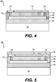
- FIG. 4 shows a cross-section view 400 of a superconducting apparatus at another stage of processing in accordance with the example.
- the superconducting apparatus includes another superconducting layer formed over dielectric layer 108.
- Vias 110 and 112 may be formed by creating via or contact holes in dielectric layer 108 and filling them with niobium or a similar superconducting material.
- Additional superconducting traces including 114, 116, and 118 are formed as part of the next superconducting layer included in the superconducting apparatus.
- the superconducting wires may be formed using niobium or other suitable metals. Niobium superconducting wires may be 0.2 micrometres wide and approximately 25 micrometres long.
- Certain such wires may be as wide as 20 micrometres and may be slotted.
- the wires may be almost as long as the length or the width of an entire die.
- the layout for the superconducting structures may be created using a place and route design tool that is used to create the layout for the superconducting wires or other elements.
- photo-resist may be patterned to protect only those areas of the superconducting layer that will be formed as superconducting wires or other structures as defined by the layout of the particular layer, such as a metal layer.
- Other superconducting metals or metal alloys may also be used as part of this step.
- the vias may be formed by conformal deposition of niobium in the same deposition step as the one used for forming the traces.
- Niobium may be deposited by sputtering or other similar processes. Other physical vapor deposition (PVD) methods, such as molecular beam epitaxy (MBE) may also be used.
- the niobium traces and vias may be formed using proximity lithography. Proximity lithography may include placing the photomask slightly lifted off the photoresist or the photo-imageable dielectric layer that is being exposed to ultra-violet light. For example, the photomask may be lifted 1 ⁇ m off the photoresist or another layer that is being exposed to the ultra-violet light. After the exposure to the light an etching step may be performed to remove the exposed areas of the photoresist or the photo-imageable dielectric layer. This step may involve using a wet etching process or a dry etching process.
- FIG. 5 shows a cross-section view 500 of at least one step used in forming a superconducting apparatus in accordance with the example.
- the superconducting apparatus includes a dielectric layer 120 formed over the superconducting traces or planes (for example the superconducting layer including superconducting traces 114, 116, and 118).
- Dielectric layer 120 is formed by depositing a dielectric (e.g., a liquid polymer) on the superconducting layer.
- Dielectric layer 120 may be formed by spinning on polyimide on the superconducting layer.
- the dielectric layer may have a thickness in a range between 1 ⁇ m and 5 ⁇ m.
- dielectric layer 120 is a photo-imageable polyimide.
- the dielectric could be HD4110 or PI-2611 having a dielectric constant of about 3.2 and having a low loss tangent of approximately 2e-4 at a temperature of 4 Kelvin for signals having a frequency of 10 GHz.
- the cure temperatures may be kept at or below 225 degrees Centigrade.
- the cure temperature for dielectric layer 120 may be selected to be lower by at least 25 degrees Centigrade than the cure temperature for dielectric layer 108.
- the cure temperature for dielectric layer 120 may be selected to be lower by at least 50 degrees Centigrade than the cure temperature for dielectric layer 108.
- FIG. 6 shows a cross-section view 600 of at least one step used in forming a superconducting apparatus subsequent to the above example.
- the superconducting apparatus may include another superconducting layer formed over dielectric layer 120. Vias may be formed by creating via or contact holes in dielectric layer 120 and filling them with niobium or a similar superconducting material. Additional superconducting traces including 124, 126, and 128 may be formed as part of the next superconducting layer included in the superconducting apparatus.
- the superconducting wires may be formed using niobium or other suitable metals. Niobium superconducting wires may be 0.2 micrometres wide and approximately 25 micrometres long.
- Certain such wires may be as wide as 20 micrometres and may be slotted.
- the wires may be almost as long as the length or the width of an entire die.
- the layout for the superconducting structures may be created using a place and route design tool that is used to create the layout for the superconducting wires or other elements.
- photo-resist may be patterned to protect only those areas of the superconducting layer that are needed to be formed as superconducting wires or other structures as defined by the layout of the particular layer, such as a metal layer.
- Other superconducting metals or metal alloys may also be used as part of this step.
- the vias may be formed by conformal deposition of niobium in the same deposition step as the one used for forming the traces.
- Niobium may be deposited by sputtering or other similar processes.
- Other physical vapor deposition (PVD) methods, such as molecular beam epitaxy (MBE) may also be used.
- the niobium traces and vias may be formed using proximity lithography. Proximity lithography may include placing the photomask slightly lifted off the photoresist or the photo-imageable dielectric layer that is being exposed to ultra-violet light. In one example, the photomask may be lifted 1 ⁇ m off the photoresist or another layer that is being exposed to the ultra-violet light. After the exposure to the light an etching step may be performed to remove the exposed areas of the photoresist or the photo-imageable dielectric layer. This step may involve using a wet etching process or a dry etching process.
- FIG. 7 shows a cross-section view 700 of at least one step used in forming a superconducting apparatus subsequent to the above example.
- the superconducting apparatus may include a dielectric layer 122 formed over superconducting traces or planes (for example the superconducting layer including superconducting traces 124, 126, and 128).
- Dielectric layer 122 may be formed by depositing a dielectric (e.g., a liquid polymer) on the superconducting layer.
- dielectric layer 122 may be formed by spinning on polyimide on the superconducting layer.
- the dielectric layer may have a thickness in a range between 1 ⁇ m and 5 ⁇ m.
- dielectric layer 122 may be a photo-imageable polyimide.
- the dielectric could be HD4110 or PI-2611 having a dielectric constant of about 3.2 and having a low loss tangent of approximately 2e-4 at a temperature of 4 Kelvin for signals having a frequency of 10 GHz. This way the formation of vias or other superconducting structures may not require the additional step of depositing a photosensitive material.
- the cure temperatures may be kept at or below 225 degrees Centigrade.
- the cure temperature for dielectric layer 122 may be selected to be lower by at least 25 degrees Centigrade than the cure temperature for dielectric layer 120.
- the cure temperature for dielectric layer 122 may be selected to be lower by at least 50 degrees Centigrade than the cure temperature for dielectric layer 120.
- the superconducting wires may be formed using niobium or other suitable metals.
- Niobium superconducting wires may be 0.2 micrometres wide and approximately 25 micrometres long. Certain such wires may be as wide as 20 micrometres and may be slotted. The wires may be almost as long as the length or the width of an entire die.
- the layout for the superconducting structures may be created using a place and route design tool that is used to create the layout for the superconducting wires or other elements.
- photo-resist may be patterned to protect only those areas of the superconducting layer that are needed to be formed as superconducting wires or other structures as defined by the layout of the particular layer, such as a metal layer.
- Other superconducting metals or metal alloys may also be used as part of this step.
- the vias may be formed by conformal deposition of niobium in the same deposition step as the one used for forming the traces.
- Niobium may be deposited by sputtering or other similar processes.
- PVD physical vapor deposition
- MBE molecular beam epitaxy
- the niobium traces and vias may be formed using proximity lithography.
- Proximity lithography may include placing the photomask slightly lifted off the photoresist or the photo-imageable dielectric layer that is being exposed to ultra-violet light.
- the photomask may be lifted 1 ⁇ m off the photoresist or another layer that is being exposed to the ultra-violet light.
- an etching step may be performed to remove the exposed areas of the photoresist or the photo-imageable dielectric layer. This step may involve using a wet etching process or a dry etching process.
- Another dielectric layer 140 may be formed as part of this stage. This layer may be formed using similar processes as described earlier.
- the cure temperatures may be kept at or below 225 degrees Centigrade.
- the cure temperature for dielectric layer 140 may be selected to be lower by at least 25 degrees Centigrade than the cure temperature for dielectric layer 122. In another example, the cure temperature for dielectric layer 140 may be selected to be lower by at least 50 degrees Centigrade than the cure temperature for dielectric layer 122.
- FIG. 7 shows a certain number of layers of the superconducting apparatus arranged in a certain manner, there could be more or fewer numbers of layers arranged differently.
- FIG. 8 shows a cross-section view 800 of at least one step used in forming a superconducting apparatus subsequent to the above example.
- vias 142 and 144 and superconducting traces 150, 152, 154, 156, and 158 may be formed.
- the superconducting wires may be formed using niobium or other suitable metals.
- Niobium superconducting wires may be 0.2 micrometres wide and approximately 25 micrometres long. Certain such wires may be as wide as 20 micrometres and may be slotted. The wires may be almost as long as the length or the width of an entire die.
- the layout for the superconducting structures may be created using a place and route design tool that is used to create the layout for the superconducting wires or other elements.
- photo-resist may be patterned to protect only those areas of the superconducting layer that are needed to be formed as superconducting wires or other structures as defined by the layout of the particular layer, such as a metal layer.
- Other superconducting metals or metal alloys may also be used as part of this step.
- the vias may be formed by conformal deposition of niobium in the same deposition step as the one used for forming the traces. Niobium may be deposited by sputtering or other similar processes.
- the niobium traces and vias may be formed using proximity lithography.
- Proximity lithography may include placing the photomask slightly lifted off the photoresist or the photo-imageable dielectric layer that is being exposed to ultra-violet light.
- the photomask may be lifted 1 ⁇ m off the photoresist or another layer that is being exposed to the ultra-violet light.
- an etching step may be performed to remove the exposed areas of the photoresist or the photo-imageable dielectric layer. This step may involve using a wet etching process or a dry etching process.
- Another dielectric layer 160 may be formed as part of this stage. This layer may be formed using similar processes as described earlier.
- the cure temperatures may be kept at or below 225 degrees Centigrade.
- the cure temperature for dielectric layer 160 may be selected to be lower by at least 25 degrees Centigrade than the cure temperature for dielectric layer 140.
- the cure temperature for dielectric layer 160 may be selected to be lower by at least 50 degrees Centigrade than the cure temperature for dielectric layer 140.
- vias 164 and 166 may be formed to provide for pad connections.
- the pad connections may be configured to support titanium/gold (Ti/Au) or titanium/aluminum (Ti/Al) pads for a variety of bump and wire bond technologies, such as Indium bump, C4 bump, or Copper pillar.
- the dielectric layers are cured at progressively lower temperatures.
- dielectric layer 104 may be cured at a temperature of 250 degrees Centigrade
- dielectric layer 108 may be cured at a temperature of 225 degrees Centigrade
- dielectric layer 120 may be cured at a temperature of 200 degrees Centigrade
- dielectric layer 122 may be cured at a temperature of 175 degrees Centigrade
- dielectric layer 140 may be cured at a temperature of 150 degrees Centigrade
- dielectric layer 160 may be cured at a temperature of 125 degrees Centigrade.
- the curing temperature difference may be less than or more than 25 degrees Centigrade.
- superconducting layer 106 may be configured to distribute clock signals through the superconducting apparatus.
- the next set of superconducting traces (e.g., superconducting traces 114, 116, and 118) may be configured to distribute clock signals through the superconducting apparatus.
- the next set of superconducting traces (e.g., superconducting traces 124, 126, and 128) may be configured to act as the ground plane for the superconducting apparatus.
- the next set of superconducting traces e.g., superconducting traces 134, 136, and 138) may be configured to distribute signals other than the clock signals through the superconducting apparatus.
- the next set of superconducting traces may be configured to distribute signals other than the clock signals through the superconducting apparatus. Indeed, the functionality of the various superconducting layers could be modified based on the requirements associated with the superconducting apparatus.
- FPGAs Field-Programmable Gate Arrays
- ASICs Application-Specific Integrated Circuits
- ASSPs Application-Specific Standard Products
- SOCs System-on-a-Chip systems
- CPLDs Complex Programmable Logic Devices
Landscapes
- Engineering & Computer Science (AREA)
- Manufacturing & Machinery (AREA)
- Chemical & Material Sciences (AREA)
- Ceramic Engineering (AREA)
- Superconductor Devices And Manufacturing Methods Thereof (AREA)
- Internal Circuitry In Semiconductor Integrated Circuit Devices (AREA)
Applications Claiming Priority (2)
| Application Number | Priority Date | Filing Date | Title |
|---|---|---|---|
| US15/715,521 US10651362B2 (en) | 2017-09-26 | 2017-09-26 | Method of forming superconducting apparatus including superconducting layers and traces |
| PCT/US2018/039214 WO2019067039A1 (en) | 2017-09-26 | 2018-06-25 | DEVICE MANUFACTURE COMPRISING SUPERCONDUCTING WIRING LAYERS AND INTERCONNECTIONS |
Publications (2)
| Publication Number | Publication Date |
|---|---|
| EP3688796A1 EP3688796A1 (en) | 2020-08-05 |
| EP3688796B1 true EP3688796B1 (en) | 2021-12-22 |
Family
ID=63077939
Family Applications (1)
| Application Number | Title | Priority Date | Filing Date |
|---|---|---|---|
| EP18749196.4A Active EP3688796B1 (en) | 2017-09-26 | 2018-06-25 | Fabrication of apparatus including superconducting wiring layers and interconnects |
Country Status (5)
| Country | Link |
|---|---|
| US (2) | US10651362B2 (https=) |
| EP (1) | EP3688796B1 (https=) |
| JP (1) | JP7170036B2 (https=) |
| AU (1) | AU2018341994B2 (https=) |
| WO (1) | WO2019067039A1 (https=) |
Families Citing this family (8)
| Publication number | Priority date | Publication date | Assignee | Title |
|---|---|---|---|---|
| US10651362B2 (en) * | 2017-09-26 | 2020-05-12 | Microsoft Technology Licensing, Llc | Method of forming superconducting apparatus including superconducting layers and traces |
| US10615223B2 (en) | 2018-06-12 | 2020-04-07 | International Business Machines Corporation | Vertical silicon-on-metal superconducting quantum interference device |
| US20200083154A1 (en) | 2018-09-10 | 2020-03-12 | At&S Austria Technologie & Systemtechnik Aktiengesellschaft | Component Carrier With a Photoimageable Dielectric Layer and a Structured Conductive Layer Being Used as a Mask for Selectively Exposing the Photoimageable Dielectric Layer With Electromagnetic Radiation |
| US11417819B2 (en) * | 2020-04-27 | 2022-08-16 | Microsoft Technology Licensing, Llc | Forming a bumpless superconductor device by bonding two substrates via a dielectric layer |
| FR3114443B1 (fr) * | 2020-09-21 | 2022-12-23 | Commissariat Energie Atomique | Structure d’intégration à routage bifonctionnel et assemblage comprenant une telle structure |
| US11742326B2 (en) * | 2020-12-28 | 2023-08-29 | Microsoft Technology Licensing, Llc | Stacked superconducting integrated circuits with three dimensional resonant clock networks |
| FR3129772B1 (fr) * | 2021-11-30 | 2024-10-04 | Commissariat Energie Atomique | Structure d’intégration destinée à connecter une pluralité de dispositifs semi-conducteurs, procédés, assemblage et système associés |
| FI20245823A1 (en) * | 2024-06-27 | 2025-12-28 | Teknologian Tutkimuskeskus Vtt Oy | Superconducting longitudinal connection and method for producing the same |
Family Cites Families (17)
| Publication number | Priority date | Publication date | Assignee | Title |
|---|---|---|---|---|
| CA1329952C (en) * | 1987-04-27 | 1994-05-31 | Yoshihiko Imanaka | Multi-layer superconducting circuit substrate and process for manufacturing same |
| JP2875093B2 (ja) * | 1992-03-17 | 1999-03-24 | 三菱電機株式会社 | 半導体装置 |
| US5476719A (en) | 1994-08-17 | 1995-12-19 | Trw Inc. | Superconducting multi-layer microstrip structure for multi-chip modules and microwave circuits |
| JPH09260378A (ja) * | 1996-03-22 | 1997-10-03 | Canon Inc | 埋め込み配線形成方法 |
| JP3457851B2 (ja) * | 1997-06-30 | 2003-10-20 | 京セラ株式会社 | 電子回路部品 |
| US6420251B1 (en) * | 1999-01-05 | 2002-07-16 | Trw Inc. | Method for fabricating a microelectronic integrated circuit with improved step coverage |
| JP4711249B2 (ja) * | 2002-08-01 | 2011-06-29 | 独立行政法人産業技術総合研究所 | 超伝導集積回路及びその作製方法 |
| EP3098865B1 (en) * | 2009-02-27 | 2018-10-03 | D-Wave Systems Inc. | Method for fabricating a superconducting integrated circuit |
| US8735326B2 (en) * | 2010-05-19 | 2014-05-27 | Northrop Grumman Systems Corporation | Methods of forming superconductor circuits |
| US9768371B2 (en) * | 2012-03-08 | 2017-09-19 | D-Wave Systems Inc. | Systems and methods for fabrication of superconducting integrated circuits |
| JP6435860B2 (ja) * | 2012-11-05 | 2018-12-19 | 大日本印刷株式会社 | 配線構造体 |
| US9741918B2 (en) * | 2013-10-07 | 2017-08-22 | Hypres, Inc. | Method for increasing the integration level of superconducting electronics circuits, and a resulting circuit |
| US10454015B2 (en) * | 2014-08-13 | 2019-10-22 | D-Wave Systems Inc. | Method of forming superconducting wiring layers with low magnetic noise |
| US9653398B1 (en) * | 2015-12-08 | 2017-05-16 | Northrop Grumman Systems Corporation | Non-oxide based dielectrics for superconductor devices |
| US10003005B2 (en) * | 2016-08-23 | 2018-06-19 | Northrop Grumman Systems Corporation | Superconductor device interconnect |
| US10276504B2 (en) * | 2017-05-17 | 2019-04-30 | Northrop Grumman Systems Corporation | Preclean and deposition methodology for superconductor interconnects |
| US10651362B2 (en) * | 2017-09-26 | 2020-05-12 | Microsoft Technology Licensing, Llc | Method of forming superconducting apparatus including superconducting layers and traces |
-
2017
- 2017-09-26 US US15/715,521 patent/US10651362B2/en active Active
-
2018
- 2018-06-25 EP EP18749196.4A patent/EP3688796B1/en active Active
- 2018-06-25 WO PCT/US2018/039214 patent/WO2019067039A1/en not_active Ceased
- 2018-06-25 AU AU2018341994A patent/AU2018341994B2/en active Active
- 2018-06-25 JP JP2020516898A patent/JP7170036B2/ja active Active
-
2020
- 2020-04-07 US US16/842,431 patent/US11114602B2/en active Active
Also Published As
| Publication number | Publication date |
|---|---|
| WO2019067039A1 (en) | 2019-04-04 |
| JP7170036B2 (ja) | 2022-11-11 |
| US20200243743A1 (en) | 2020-07-30 |
| US20190097118A1 (en) | 2019-03-28 |
| EP3688796A1 (en) | 2020-08-05 |
| AU2018341994B2 (en) | 2022-09-29 |
| AU2018341994A1 (en) | 2020-02-20 |
| US10651362B2 (en) | 2020-05-12 |
| JP2020535643A (ja) | 2020-12-03 |
| US11114602B2 (en) | 2021-09-07 |
Similar Documents
| Publication | Publication Date | Title |
|---|---|---|
| EP3688796B1 (en) | Fabrication of apparatus including superconducting wiring layers and interconnects | |
| US12518977B2 (en) | Signal distribution for a quantum computing system | |
| US10134972B2 (en) | Qubit and coupler circuit structures and coupling techniques | |
| AU2018413356B2 (en) | Computing system with superconducting and non-superconducting components located on a common substrate | |
| US10658424B2 (en) | Superconducting integrated circuit | |
| Ho et al. | High RF performance TSV silicon carrier for high frequency application | |
| CN112272811B (zh) | 具有使用金属预成型件的热管理的低温计算系统 | |
| JP2019532505A (ja) | 積層量子デバイス内の損失の低減 | |
| WO2017131831A2 (en) | Qubit and coupler circuit structures and coupling techniques | |
| CN121843229A (zh) | 半导体器件及其制造方法 | |
| HK40032665A (en) | Computing system with superconducting and nonsuperconducting components located on a common substrate | |
| HK40032665B (en) | Computing system with superconducting and nonsuperconducting components located on a common substrate |
Legal Events
| Date | Code | Title | Description |
|---|---|---|---|
| STAA | Information on the status of an ep patent application or granted ep patent |
Free format text: STATUS: UNKNOWN |
|
| STAA | Information on the status of an ep patent application or granted ep patent |
Free format text: STATUS: THE INTERNATIONAL PUBLICATION HAS BEEN MADE |
|
| PUAI | Public reference made under article 153(3) epc to a published international application that has entered the european phase |
Free format text: ORIGINAL CODE: 0009012 |
|
| STAA | Information on the status of an ep patent application or granted ep patent |
Free format text: STATUS: REQUEST FOR EXAMINATION WAS MADE |
|
| 17P | Request for examination filed |
Effective date: 20200219 |
|
| AK | Designated contracting states |
Kind code of ref document: A1 Designated state(s): AL AT BE BG CH CY CZ DE DK EE ES FI FR GB GR HR HU IE IS IT LI LT LU LV MC MK MT NL NO PL PT RO RS SE SI SK SM TR |
|
| AX | Request for extension of the european patent |
Extension state: BA ME |
|
| DAV | Request for validation of the european patent (deleted) | ||
| DAX | Request for extension of the european patent (deleted) | ||
| GRAP | Despatch of communication of intention to grant a patent |
Free format text: ORIGINAL CODE: EPIDOSNIGR1 |
|
| STAA | Information on the status of an ep patent application or granted ep patent |
Free format text: STATUS: GRANT OF PATENT IS INTENDED |
|
| INTG | Intention to grant announced |
Effective date: 20210812 |
|
| RIN1 | Information on inventor provided before grant (corrected) |
Inventor name: TUCKERMAN, DAVID B. Inventor name: ROUSE, RICHARD P. |
|
| RAP3 | Party data changed (applicant data changed or rights of an application transferred) |
Owner name: MICROSOFT TECHNOLOGY LICENSING, LLC |
|
| GRAS | Grant fee paid |
Free format text: ORIGINAL CODE: EPIDOSNIGR3 |
|
| GRAA | (expected) grant |
Free format text: ORIGINAL CODE: 0009210 |
|
| STAA | Information on the status of an ep patent application or granted ep patent |
Free format text: STATUS: THE PATENT HAS BEEN GRANTED |
|
| AK | Designated contracting states |
Kind code of ref document: B1 Designated state(s): AL AT BE BG CH CY CZ DE DK EE ES FI FR GB GR HR HU IE IS IT LI LT LU LV MC MK MT NL NO PL PT RO RS SE SI SK SM TR |
|
| REG | Reference to a national code |
Ref country code: GB Ref legal event code: FG4D |
|
| REG | Reference to a national code |
Ref country code: CH Ref legal event code: EP |
|
| REG | Reference to a national code |
Ref country code: DE Ref legal event code: R096 Ref document number: 602018028540 Country of ref document: DE |
|
| REG | Reference to a national code |
Ref country code: AT Ref legal event code: REF Ref document number: 1457627 Country of ref document: AT Kind code of ref document: T Effective date: 20220115 |
|
| REG | Reference to a national code |
Ref country code: IE Ref legal event code: FG4D |
|
| REG | Reference to a national code |
Ref country code: NL Ref legal event code: FP |
|
| REG | Reference to a national code |
Ref country code: LT Ref legal event code: MG9D |
|
| PG25 | Lapsed in a contracting state [announced via postgrant information from national office to epo] |
Ref country code: RS Free format text: LAPSE BECAUSE OF FAILURE TO SUBMIT A TRANSLATION OF THE DESCRIPTION OR TO PAY THE FEE WITHIN THE PRESCRIBED TIME-LIMIT Effective date: 20211222 Ref country code: LT Free format text: LAPSE BECAUSE OF FAILURE TO SUBMIT A TRANSLATION OF THE DESCRIPTION OR TO PAY THE FEE WITHIN THE PRESCRIBED TIME-LIMIT Effective date: 20211222 Ref country code: FI Free format text: LAPSE BECAUSE OF FAILURE TO SUBMIT A TRANSLATION OF THE DESCRIPTION OR TO PAY THE FEE WITHIN THE PRESCRIBED TIME-LIMIT Effective date: 20211222 Ref country code: BG Free format text: LAPSE BECAUSE OF FAILURE TO SUBMIT A TRANSLATION OF THE DESCRIPTION OR TO PAY THE FEE WITHIN THE PRESCRIBED TIME-LIMIT Effective date: 20220322 |
|
| REG | Reference to a national code |
Ref country code: AT Ref legal event code: MK05 Ref document number: 1457627 Country of ref document: AT Kind code of ref document: T Effective date: 20211222 |
|
| PG25 | Lapsed in a contracting state [announced via postgrant information from national office to epo] |
Ref country code: SE Free format text: LAPSE BECAUSE OF FAILURE TO SUBMIT A TRANSLATION OF THE DESCRIPTION OR TO PAY THE FEE WITHIN THE PRESCRIBED TIME-LIMIT Effective date: 20211222 Ref country code: NO Free format text: LAPSE BECAUSE OF FAILURE TO SUBMIT A TRANSLATION OF THE DESCRIPTION OR TO PAY THE FEE WITHIN THE PRESCRIBED TIME-LIMIT Effective date: 20220322 Ref country code: LV Free format text: LAPSE BECAUSE OF FAILURE TO SUBMIT A TRANSLATION OF THE DESCRIPTION OR TO PAY THE FEE WITHIN THE PRESCRIBED TIME-LIMIT Effective date: 20211222 Ref country code: HR Free format text: LAPSE BECAUSE OF FAILURE TO SUBMIT A TRANSLATION OF THE DESCRIPTION OR TO PAY THE FEE WITHIN THE PRESCRIBED TIME-LIMIT Effective date: 20211222 Ref country code: GR Free format text: LAPSE BECAUSE OF FAILURE TO SUBMIT A TRANSLATION OF THE DESCRIPTION OR TO PAY THE FEE WITHIN THE PRESCRIBED TIME-LIMIT Effective date: 20220323 |
|
| PG25 | Lapsed in a contracting state [announced via postgrant information from national office to epo] |
Ref country code: SM Free format text: LAPSE BECAUSE OF FAILURE TO SUBMIT A TRANSLATION OF THE DESCRIPTION OR TO PAY THE FEE WITHIN THE PRESCRIBED TIME-LIMIT Effective date: 20211222 Ref country code: SK Free format text: LAPSE BECAUSE OF FAILURE TO SUBMIT A TRANSLATION OF THE DESCRIPTION OR TO PAY THE FEE WITHIN THE PRESCRIBED TIME-LIMIT Effective date: 20211222 Ref country code: RO Free format text: LAPSE BECAUSE OF FAILURE TO SUBMIT A TRANSLATION OF THE DESCRIPTION OR TO PAY THE FEE WITHIN THE PRESCRIBED TIME-LIMIT Effective date: 20211222 Ref country code: PT Free format text: LAPSE BECAUSE OF FAILURE TO SUBMIT A TRANSLATION OF THE DESCRIPTION OR TO PAY THE FEE WITHIN THE PRESCRIBED TIME-LIMIT Effective date: 20220422 Ref country code: ES Free format text: LAPSE BECAUSE OF FAILURE TO SUBMIT A TRANSLATION OF THE DESCRIPTION OR TO PAY THE FEE WITHIN THE PRESCRIBED TIME-LIMIT Effective date: 20211222 Ref country code: EE Free format text: LAPSE BECAUSE OF FAILURE TO SUBMIT A TRANSLATION OF THE DESCRIPTION OR TO PAY THE FEE WITHIN THE PRESCRIBED TIME-LIMIT Effective date: 20211222 Ref country code: CZ Free format text: LAPSE BECAUSE OF FAILURE TO SUBMIT A TRANSLATION OF THE DESCRIPTION OR TO PAY THE FEE WITHIN THE PRESCRIBED TIME-LIMIT Effective date: 20211222 |
|
| PG25 | Lapsed in a contracting state [announced via postgrant information from national office to epo] |
Ref country code: PL Free format text: LAPSE BECAUSE OF FAILURE TO SUBMIT A TRANSLATION OF THE DESCRIPTION OR TO PAY THE FEE WITHIN THE PRESCRIBED TIME-LIMIT Effective date: 20211222 Ref country code: AT Free format text: LAPSE BECAUSE OF FAILURE TO SUBMIT A TRANSLATION OF THE DESCRIPTION OR TO PAY THE FEE WITHIN THE PRESCRIBED TIME-LIMIT Effective date: 20211222 |
|
| REG | Reference to a national code |
Ref country code: DE Ref legal event code: R097 Ref document number: 602018028540 Country of ref document: DE |
|
| PG25 | Lapsed in a contracting state [announced via postgrant information from national office to epo] |
Ref country code: IS Free format text: LAPSE BECAUSE OF FAILURE TO SUBMIT A TRANSLATION OF THE DESCRIPTION OR TO PAY THE FEE WITHIN THE PRESCRIBED TIME-LIMIT Effective date: 20220422 |
|
| PLBE | No opposition filed within time limit |
Free format text: ORIGINAL CODE: 0009261 |
|
| STAA | Information on the status of an ep patent application or granted ep patent |
Free format text: STATUS: NO OPPOSITION FILED WITHIN TIME LIMIT |
|
| PG25 | Lapsed in a contracting state [announced via postgrant information from national office to epo] |
Ref country code: DK Free format text: LAPSE BECAUSE OF FAILURE TO SUBMIT A TRANSLATION OF THE DESCRIPTION OR TO PAY THE FEE WITHIN THE PRESCRIBED TIME-LIMIT Effective date: 20211222 Ref country code: AL Free format text: LAPSE BECAUSE OF FAILURE TO SUBMIT A TRANSLATION OF THE DESCRIPTION OR TO PAY THE FEE WITHIN THE PRESCRIBED TIME-LIMIT Effective date: 20211222 |
|
| 26N | No opposition filed |
Effective date: 20220923 |
|
| PG25 | Lapsed in a contracting state [announced via postgrant information from national office to epo] |
Ref country code: MC Free format text: LAPSE BECAUSE OF FAILURE TO SUBMIT A TRANSLATION OF THE DESCRIPTION OR TO PAY THE FEE WITHIN THE PRESCRIBED TIME-LIMIT Effective date: 20211222 |
|
| REG | Reference to a national code |
Ref country code: CH Ref legal event code: PL |
|
| REG | Reference to a national code |
Ref country code: BE Ref legal event code: MM Effective date: 20220630 |
|
| PG25 | Lapsed in a contracting state [announced via postgrant information from national office to epo] |
Ref country code: SI Free format text: LAPSE BECAUSE OF FAILURE TO SUBMIT A TRANSLATION OF THE DESCRIPTION OR TO PAY THE FEE WITHIN THE PRESCRIBED TIME-LIMIT Effective date: 20211222 |
|
| PG25 | Lapsed in a contracting state [announced via postgrant information from national office to epo] |
Ref country code: LU Free format text: LAPSE BECAUSE OF NON-PAYMENT OF DUE FEES Effective date: 20220625 Ref country code: LI Free format text: LAPSE BECAUSE OF NON-PAYMENT OF DUE FEES Effective date: 20220630 Ref country code: IE Free format text: LAPSE BECAUSE OF NON-PAYMENT OF DUE FEES Effective date: 20220625 Ref country code: CH Free format text: LAPSE BECAUSE OF NON-PAYMENT OF DUE FEES Effective date: 20220630 |
|
| PG25 | Lapsed in a contracting state [announced via postgrant information from national office to epo] |
Ref country code: IT Free format text: LAPSE BECAUSE OF FAILURE TO SUBMIT A TRANSLATION OF THE DESCRIPTION OR TO PAY THE FEE WITHIN THE PRESCRIBED TIME-LIMIT Effective date: 20211222 Ref country code: BE Free format text: LAPSE BECAUSE OF NON-PAYMENT OF DUE FEES Effective date: 20220630 |
|
| P01 | Opt-out of the competence of the unified patent court (upc) registered |
Effective date: 20230501 |
|
| PG25 | Lapsed in a contracting state [announced via postgrant information from national office to epo] |
Ref country code: MK Free format text: LAPSE BECAUSE OF FAILURE TO SUBMIT A TRANSLATION OF THE DESCRIPTION OR TO PAY THE FEE WITHIN THE PRESCRIBED TIME-LIMIT Effective date: 20211222 Ref country code: CY Free format text: LAPSE BECAUSE OF FAILURE TO SUBMIT A TRANSLATION OF THE DESCRIPTION OR TO PAY THE FEE WITHIN THE PRESCRIBED TIME-LIMIT Effective date: 20211222 |
|
| PG25 | Lapsed in a contracting state [announced via postgrant information from national office to epo] |
Ref country code: HU Free format text: LAPSE BECAUSE OF FAILURE TO SUBMIT A TRANSLATION OF THE DESCRIPTION OR TO PAY THE FEE WITHIN THE PRESCRIBED TIME-LIMIT; INVALID AB INITIO Effective date: 20180625 |
|
| PG25 | Lapsed in a contracting state [announced via postgrant information from national office to epo] |
Ref country code: MT Free format text: LAPSE BECAUSE OF FAILURE TO SUBMIT A TRANSLATION OF THE DESCRIPTION OR TO PAY THE FEE WITHIN THE PRESCRIBED TIME-LIMIT Effective date: 20211222 |
|
| PGFP | Annual fee paid to national office [announced via postgrant information from national office to epo] |
Ref country code: NL Payment date: 20250520 Year of fee payment: 8 |
|
| PGFP | Annual fee paid to national office [announced via postgrant information from national office to epo] |
Ref country code: DE Payment date: 20250520 Year of fee payment: 8 |
|
| PGFP | Annual fee paid to national office [announced via postgrant information from national office to epo] |
Ref country code: GB Payment date: 20250520 Year of fee payment: 8 |
|
| PGFP | Annual fee paid to national office [announced via postgrant information from national office to epo] |
Ref country code: FR Payment date: 20250520 Year of fee payment: 8 |
|
| REG | Reference to a national code |
Ref country code: DE Ref legal event code: R079 Ref document number: 602018028540 Country of ref document: DE Free format text: PREVIOUS MAIN CLASS: H01L0021768000 Ipc: H10W0020000000 |
|
| PG25 | Lapsed in a contracting state [announced via postgrant information from national office to epo] |
Ref country code: TR Free format text: LAPSE BECAUSE OF FAILURE TO SUBMIT A TRANSLATION OF THE DESCRIPTION OR TO PAY THE FEE WITHIN THE PRESCRIBED TIME-LIMIT Effective date: 20211222 |