EP3687192B1 - Mikroelektromechanischer elektroakustischer wandler mit piezoelektrischer betätigung und entsprechendes herstellungsverfahren - Google Patents
Mikroelektromechanischer elektroakustischer wandler mit piezoelektrischer betätigung und entsprechendes herstellungsverfahren Download PDFInfo
- Publication number
- EP3687192B1 EP3687192B1 EP20153473.2A EP20153473A EP3687192B1 EP 3687192 B1 EP3687192 B1 EP 3687192B1 EP 20153473 A EP20153473 A EP 20153473A EP 3687192 B1 EP3687192 B1 EP 3687192B1
- Authority
- EP
- European Patent Office
- Prior art keywords
- cantilever elements
- stopper
- buried
- actuator element
- cavity
- Prior art date
- Legal status (The legal status is an assumption and is not a legal conclusion. Google has not performed a legal analysis and makes no representation as to the accuracy of the status listed.)
- Active
Links
Images


Classifications
-
- H—ELECTRICITY
- H04—ELECTRIC COMMUNICATION TECHNIQUE
- H04R—LOUDSPEAKERS, MICROPHONES, GRAMOPHONE PICK-UPS OR LIKE ACOUSTIC ELECTROMECHANICAL TRANSDUCERS; ELECTRIC HEARING AIDS; PUBLIC ADDRESS SYSTEMS
- H04R19/00—Electrostatic transducers
- H04R19/005—Electrostatic transducers using semiconductor materials
-
- H—ELECTRICITY
- H04—ELECTRIC COMMUNICATION TECHNIQUE
- H04R—LOUDSPEAKERS, MICROPHONES, GRAMOPHONE PICK-UPS OR LIKE ACOUSTIC ELECTROMECHANICAL TRANSDUCERS; ELECTRIC HEARING AIDS; PUBLIC ADDRESS SYSTEMS
- H04R19/00—Electrostatic transducers
- H04R19/02—Loudspeakers
-
- B—PERFORMING OPERATIONS; TRANSPORTING
- B81—MICROSTRUCTURAL TECHNOLOGY
- B81B—MICROSTRUCTURAL DEVICES OR SYSTEMS, e.g. MICROMECHANICAL DEVICES
- B81B3/00—Devices comprising flexible or deformable elements, e.g. comprising elastic tongues or membranes
- B81B3/0035—Constitution or structural means for controlling the movement of the flexible or deformable elements
- B81B3/0051—For defining the movement, i.e. structures that guide or limit the movement of an element
-
- B—PERFORMING OPERATIONS; TRANSPORTING
- B81—MICROSTRUCTURAL TECHNOLOGY
- B81C—PROCESSES OR APPARATUS SPECIALLY ADAPTED FOR THE MANUFACTURE OR TREATMENT OF MICROSTRUCTURAL DEVICES OR SYSTEMS
- B81C1/00—Manufacture or treatment of devices or systems in or on a substrate
- B81C1/00015—Manufacture or treatment of devices or systems in or on a substrate for manufacturing microsystems
- B81C1/00134—Manufacture or treatment of devices or systems in or on a substrate for manufacturing microsystems comprising flexible or deformable structures
- B81C1/0015—Cantilevers
-
- H—ELECTRICITY
- H04—ELECTRIC COMMUNICATION TECHNIQUE
- H04R—LOUDSPEAKERS, MICROPHONES, GRAMOPHONE PICK-UPS OR LIKE ACOUSTIC ELECTROMECHANICAL TRANSDUCERS; ELECTRIC HEARING AIDS; PUBLIC ADDRESS SYSTEMS
- H04R1/00—Details of transducers, loudspeakers or microphones
- H04R1/02—Casings; Cabinets ; Supports therefor; Mountings therein
- H04R1/025—Arrangements for fixing loudspeaker transducers, e.g. in a box, furniture
-
- H—ELECTRICITY
- H04—ELECTRIC COMMUNICATION TECHNIQUE
- H04R—LOUDSPEAKERS, MICROPHONES, GRAMOPHONE PICK-UPS OR LIKE ACOUSTIC ELECTROMECHANICAL TRANSDUCERS; ELECTRIC HEARING AIDS; PUBLIC ADDRESS SYSTEMS
- H04R31/00—Apparatus or processes specially adapted for the manufacture of transducers or diaphragms therefor
- H04R31/006—Interconnection of transducer parts
-
- B—PERFORMING OPERATIONS; TRANSPORTING
- B81—MICROSTRUCTURAL TECHNOLOGY
- B81B—MICROSTRUCTURAL DEVICES OR SYSTEMS, e.g. MICROMECHANICAL DEVICES
- B81B2201/00—Specific applications of microelectromechanical systems
- B81B2201/02—Sensors
- B81B2201/0257—Microphones or microspeakers
-
- B—PERFORMING OPERATIONS; TRANSPORTING
- B81—MICROSTRUCTURAL TECHNOLOGY
- B81B—MICROSTRUCTURAL DEVICES OR SYSTEMS, e.g. MICROMECHANICAL DEVICES
- B81B2203/00—Basic microelectromechanical structures
- B81B2203/01—Suspended structures, i.e. structures allowing a movement
- B81B2203/0118—Cantilevers
-
- B—PERFORMING OPERATIONS; TRANSPORTING
- B81—MICROSTRUCTURAL TECHNOLOGY
- B81B—MICROSTRUCTURAL DEVICES OR SYSTEMS, e.g. MICROMECHANICAL DEVICES
- B81B2203/00—Basic microelectromechanical structures
- B81B2203/01—Suspended structures, i.e. structures allowing a movement
- B81B2203/0127—Diaphragms, i.e. structures separating two media that can control the passage from one medium to another; Membranes, i.e. diaphragms with filtering function
-
- B—PERFORMING OPERATIONS; TRANSPORTING
- B81—MICROSTRUCTURAL TECHNOLOGY
- B81B—MICROSTRUCTURAL DEVICES OR SYSTEMS, e.g. MICROMECHANICAL DEVICES
- B81B2203/00—Basic microelectromechanical structures
- B81B2203/03—Static structures
- B81B2203/0315—Cavities
-
- B—PERFORMING OPERATIONS; TRANSPORTING
- B81—MICROSTRUCTURAL TECHNOLOGY
- B81C—PROCESSES OR APPARATUS SPECIALLY ADAPTED FOR THE MANUFACTURE OR TREATMENT OF MICROSTRUCTURAL DEVICES OR SYSTEMS
- B81C2201/00—Manufacture or treatment of microstructural devices or systems
- B81C2201/01—Manufacture or treatment of microstructural devices or systems in or on a substrate
- B81C2201/0101—Shaping material; Structuring the bulk substrate or layers on the substrate; Film patterning
- B81C2201/0111—Bulk micromachining
- B81C2201/0116—Thermal treatment for structural rearrangement of substrate atoms, e.g. for making buried cavities
-
- B—PERFORMING OPERATIONS; TRANSPORTING
- B81—MICROSTRUCTURAL TECHNOLOGY
- B81C—PROCESSES OR APPARATUS SPECIALLY ADAPTED FOR THE MANUFACTURE OR TREATMENT OF MICROSTRUCTURAL DEVICES OR SYSTEMS
- B81C2201/00—Manufacture or treatment of microstructural devices or systems
- B81C2201/01—Manufacture or treatment of microstructural devices or systems in or on a substrate
- B81C2201/0101—Shaping material; Structuring the bulk substrate or layers on the substrate; Film patterning
- B81C2201/0128—Processes for removing material
- B81C2201/013—Etching
- B81C2201/0133—Wet etching
-
- B—PERFORMING OPERATIONS; TRANSPORTING
- B81—MICROSTRUCTURAL TECHNOLOGY
- B81C—PROCESSES OR APPARATUS SPECIALLY ADAPTED FOR THE MANUFACTURE OR TREATMENT OF MICROSTRUCTURAL DEVICES OR SYSTEMS
- B81C2201/00—Manufacture or treatment of microstructural devices or systems
- B81C2201/01—Manufacture or treatment of microstructural devices or systems in or on a substrate
- B81C2201/0174—Manufacture or treatment of microstructural devices or systems in or on a substrate for making multi-layered devices, film deposition or growing
- B81C2201/0176—Chemical vapour Deposition
- B81C2201/0178—Oxidation
-
- H—ELECTRICITY
- H04—ELECTRIC COMMUNICATION TECHNIQUE
- H04R—LOUDSPEAKERS, MICROPHONES, GRAMOPHONE PICK-UPS OR LIKE ACOUSTIC ELECTROMECHANICAL TRANSDUCERS; ELECTRIC HEARING AIDS; PUBLIC ADDRESS SYSTEMS
- H04R17/00—Piezoelectric transducers; Electrostrictive transducers
-
- H—ELECTRICITY
- H04—ELECTRIC COMMUNICATION TECHNIQUE
- H04R—LOUDSPEAKERS, MICROPHONES, GRAMOPHONE PICK-UPS OR LIKE ACOUSTIC ELECTROMECHANICAL TRANSDUCERS; ELECTRIC HEARING AIDS; PUBLIC ADDRESS SYSTEMS
- H04R2201/00—Details of transducers, loudspeakers or microphones covered by H04R1/00 but not provided for in any of its subgroups
- H04R2201/003—Mems transducers or their use
-
- H—ELECTRICITY
- H04—ELECTRIC COMMUNICATION TECHNIQUE
- H04R—LOUDSPEAKERS, MICROPHONES, GRAMOPHONE PICK-UPS OR LIKE ACOUSTIC ELECTROMECHANICAL TRANSDUCERS; ELECTRIC HEARING AIDS; PUBLIC ADDRESS SYSTEMS
- H04R2400/00—Loudspeakers
- H04R2400/11—Aspects regarding the frame of loudspeaker transducers
Definitions
- the present solution relates to a microelectromechanical electroacoustic transducer with piezoelectric actuation (made with MEMS, Micro-ElectroMechanical Systems, technology) and to a corresponding manufacturing process; in particular, hereinafter reference will be made, without thereby this implying any loss of generality, to a MEMS transducer operating as actuator for the generation of sound waves, i.e., to a MEMS speaker.
- electromagnetically actuated speakers are currently the most widely used, for example for headphones, earpieces, and diffusers for portable devices (such as smartphones, tablets or the like).
- transducers of the so-called BA (Balanced Armature Driver) type based on the principle of electromagnetic actuation, envisage use of an electrical signal to set in vibration a thin lamina arranged between two magnetic windings. The movement of this lamina is transferred to a diaphragm, generally made of aluminum, for the generation of acoustic signals in the audio band.
- piezoelectric MEMS transducers with respect to traditional electromagnetically actuated transducers, can offer considerable advantages, which are particularly relevant for use in portable electronic devices, amongst which: an increase in the precision of mechanical actuation; a better fidelity in audio reproduction; and reduced cost, weight, and size.
- transducers of the BA type do not have a flat frequency response in the audio band and suffer from relevant resonance effects; instead, piezoelectric MEMS transducers may in general have a flatter frequency response and a faster dynamic response.
- piezoelectric MEMS transducers can guarantee preservation of the acoustic integrity even after being completely immersed in a liquid or a powder medium.
- piezoelectric MEMS transducers have a lower mechanical strength, being more subject to damages in the case of dropping or impact (an event that is, on the other hand, rather frequent in the case of use in portable devices).
- US 2017/0085994 A1 discloses a piezoelectric MEMS transducer having a stopper structure aimed at reducing the risk of breaking of a corresponding acoustic membrane.
- this piezoelectric MEMS transducer As illustrated in Figure 1 , this piezoelectric MEMS transducer, designated as a whole by 1, comprises a die 2 of semiconductor material, including a supporting substrate 3, which is frame-shaped and surrounds a coupling element 4 (formed in the same die 2).
- the piezoelectric MEMS transducer 1 further comprises a housing structure 6, having: a bottom part 6a, which is coupled to the first surface 2a of the die 2, underneath the actuation structure 5, and defines a cavity, above which the same actuation structure 5 is suspended; a central part 6b, laterally coupled to the die 2; and a top part 6c, coupled above a second surface 2b of the die 2, opposite in a vertical direction to the first surface 2a.
- the aforesaid top part 6c of the housing structure 6 carries an acoustic membrane 7, having a funnel-shape and centrally coupled to the coupling element 4.
- the piezoelectric MEMS transducer 1 further comprises a stopper mechanism 8, constituted by: a reinforcement element 9a, coupled (in particular glued) to the acoustic membrane 7 and having the same funnel shape; and a stopper element 9b, constituted by the surface of the same supporting substrate 3 at the second surface 2b of the die 2, which is facing the aforesaid reinforcement element 9a normally at a certain separation distance, in the resting position of the acoustic membrane 7.
- a stopper mechanism 8 constituted by: a reinforcement element 9a, coupled (in particular glued) to the acoustic membrane 7 and having the same funnel shape; and a stopper element 9b, constituted by the surface of the same supporting substrate 3 at the second surface 2b of the die 2, which is facing the aforesaid reinforcement element 9a normally at a certain separation distance, in the resting position of the acoustic membrane 7.
- the stopper mechanism 8 acts so as to limit the maximum deflection of the acoustic membrane 7 in a vertical direction, only towards the bottom part 6a of the housing structure 6, so as to reduce, in part, the possibility of breaking of the acoustic membrane 7 in the case of impact or dropping.
- the piezoelectric MEMS transducer 1 has some limitations that do not enable complete exploitation of its advantageous characteristics.
- the stopper mechanism 8 safeguards the acoustic membrane 7 from breaking as a result of movements that occur only in one direction of the aforesaid vertical axis, and the piezoelectric MEMS transducer 1 does not have any stopper arrangement for safeguarding the actuation structure 5 and the corresponding layer of piezoelectric material from failures; the same actuation structure 5, in the case of impact or dropping, may thus be damaged and jeopardise operation of the piezoelectric MEMS transducer 1.
- the aim of the present solution is to provide a microelectromechanical electroacoustic transducer with piezoelectric actuation that will enable the drawbacks of the prior art to be overcome.
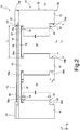
- an actuation structure 10 of a MEMS electroacoustic transducer 11 (which will be illustrated in greater detail hereinafter), according to a first embodiment of the present solution, is now disclosed.
- the actuation structure 10 is made in a die 12, comprising a monolithic body 13 of semiconductor material, in particular monocrystalline silicon, having a front surface 13a and a rear surface 13b.
- the actuation structure 10 comprises, in the same monolithic body 13, a frame 14 and an actuator element 15.
- the frame 14 surrounds the actuator element 15 and is separated from the actuator element 15 by a central opening 16; the actuator element 15 is arranged in a central position with respect to the central opening 16 and is pillar-shaped.
- the actuation structure 10 further comprises, also provided in the same monolithic body 13, in a surface portion (at the front surface 13a), cantilever elements 18, which are suspended above the central opening 16 and extend between the frame 14 and the actuator element 15.
- Each cantilever element 18 has a first end coupled to the frame 14 and a second end coupled to the actuator element 15, at a coupling portion 15' thereof.
- the coupling between the cantilever elements 18 and the actuator element 15 is through elastic coupling elements 17 (illustrated schematically in Figure 3 ).
- the actuation structure 10 further comprises: piezoelectric regions 19, arranged on the cantilever elements 18, formed by one or more overlying layers including piezoelectric material (in a known way, here not described in detail); and a passivation layer 20, made of dielectric material, arranged on the piezoelectric regions 19. In the embodiment illustrated, the layers of piezoelectric material extend also over the actuator element 15.
- Electrical-connection paths 22 are arranged over the passivation layer 20 and cross the same passivation layer 20 inside contact openings 23, to achieve the electrical connection with the piezoelectric regions 19 and enable biasing thereof by means of appropriate electrical signals.
- the central opening 16 extends vertically (along a vertical axis z orthogonal to a horizontal plane xy in which the aforesaid front and rear surfaces 13a, 13b of the monolithic body 13 lie) starting from the rear surface 13b of the monolithic body 13 up to the cantilever elements 18, which are arranged at the front surface 13a of the same monolithic body 13.
- the central opening 16 has: a first width L1 (in the direction of longitudinal extension of the cantilever elements 18 in the horizontal plane xy, along a first horizontal axis x) at the front surface 13a of the monolithic body 13, directly underneath the cantilever elements 18; a second width L2 through the thickness of the monolithic body 13; and a third width L3 at the rear surface 13b of the monolithic body 13.
- the first width L1 is greater than the second width L2
- the third width L3 is greater than the second width L2 (possibly, the third width L3 being equal to the first width L1) .
- first recesses 25a are defined along a vertical wall of the frame 14, facing the central opening 16, in a position vertically corresponding to the coupling portions with the cantilever elements 18 and in the proximity of the front surface 13a of the monolithic body 13; likewise, second recesses 25b are defined along the same vertical wall of the frame 14, at the rear surface 13b of the monolithic body 13.
- respective first recesses 26a obtained in the corresponding coupling portion 15'
- respective second recesses 26b at the rear surface 13b of the monolithic body 13.
- the actuation structure 10 comprises a first stopper arrangement 30, made integrally to the die 12 and the monolithic body 13, configured to stop movement along a first direction of the vertical axis z, in particular to stop movement of the cantilever elements 18 towards the underlying central opening 16.
- the first stopper arrangement 30 is defined by the first recesses 25a of the frame 14, which determine a first stopper surface 30' facing the cantilever elements 18, arranged at a certain distance d1 (in the vertical direction) from the cantilever elements 18, in the resting condition, i.e., in the absence of any deformation, of the cantilever elements 18 (the distance d1 moreover corresponding to the distance between the stopper surface 30' and the front surface 13a of the monolithic body 13).
- the respective first recesses 26a of the actuator element 15 can contribute to defining a further stopper arrangement 30, thus contributing to stopping movement of the cantilever elements 18 along the vertical direction, at the same actuator element 15.
- the actuation structure 10 further comprises a second stopper arrangement 32, which is also made integrally to the die 12 and the monolithic body 13, configured to limit movement of the cantilever elements 18 along a second direction of the vertical axis z (opposite to the first direction), and, as will be highlighted hereinafter, movement in the second direction of an acoustic membrane that is designed to be coupled to the actuator element 15 at the rear surface 13b of the monolithic body 13.
- a second stopper arrangement 32 which is also made integrally to the die 12 and the monolithic body 13, configured to limit movement of the cantilever elements 18 along a second direction of the vertical axis z (opposite to the first direction), and, as will be highlighted hereinafter, movement in the second direction of an acoustic membrane that is designed to be coupled to the actuator element 15 at the rear surface 13b of the monolithic body 13.
- the aforesaid second stopper arrangement 30 is defined by the second recesses 25b of the frame 14, which define a second stopper surface 32', which is designed to face a stopper element coupled to the aforesaid acoustic membrane, arranged at a certain distance d2 (in the vertical direction) with respect to the stopper element, in the resting condition, i.e., in the absence of deformations (the distance d2 moreover corresponding to the distance between the second stopper surface 32' and the rear surface 13b of the monolithic body 13) .
- the respective second recesses 26b of the actuator element 15 contribute, as on the other hand will be clear hereinafter, to limit adhesion of the actuator element 15 to an adhesive tape during the manufacturing steps, with the aim of reducing possible mechanical failures of the cantilever elements 18 during detachment of the frame 14 from the tape in the assembly steps.
- the first and the second stopper arrangements 30, 32 thus jointly define a bi-directional stopper mechanism along the vertical axis z, for limiting and stopping the movements of the actuation structure 10, thus effectively reducing the possibility of breaking in case of impact or dropping.
- the aforesaid central opening 16 has a generically circular shape in plan view and the cantilever elements 18, four in number in the example represented, have a generically triangular shape in plan view and are arranged, in pairs, on opposite sides of the actuator element 15, along diametral directions.
- the elastic coupling elements 17 that couple each cantilever element 18 to the coupling portion 15' of the actuator element 15 may have a configuration of a folded type.
- Figure 4 shows, in an assembled condition, a first embodiment of the MEMS electroacoustic transducer 11, which comprises the actuation structure 10 and moreover a rigid lamina 34, coupled to the actuator element 15, on the rear surface 13b of the monolithic body 13.
- the rigid lamina 34 has a side extension (parallel to the extension of the cantilever elements 18 along the axis x) greater than the extension of the central opening 16, so as to have end portions facing the second stopper surface 32' of the second stopper arrangement 32, at the distance d2 from the second stopper surface 32' in the resting condition.
- the MEMS electroacoustic transducer 11 further comprises a thin acoustic membrane 35, centrally coupled (for example, glued) to the rigid lamina 34 only at a corresponding central portion and supported at respective ends by supporting elements 36, coupled (for example, glued) on the rear surface 13b of the monolithic body 13 around the frame 14.
- the acoustic membrane 35 has a concave funnel shape and undergoes deformation, during operation, following movement of the actuator element 15 due to deformation by the reverse piezoelectric effect of the piezoelectric regions 19, thus generating sound waves in the audio band (the actuator element 15 hence acting as a piston actuator along the vertical axis z).
- the first stopper arrangement 30 enables stopping movement of the cantilever elements 18 and of the acoustic membrane 35 in a first direction of the vertical axis z (in the representation of Figure 4 , upwards).
- the end portions of the stopper elements 18 abut against the facing surface (first stopper surface 30') of the first stopper arrangement 30, thus stopping their movement.
- the second stopper arrangement 32 enables stopping movement of the acoustic membrane 35 and of the cantilever elements 18 in the second direction of the vertical axis z (in the representation of Figure 4 , downwards).
- the rigid lamina 34 constitutes a stopper element that abuts against the facing surface (second stopper surface 32') of the second stopper arrangement 32, thus stopping the movement.
- FIG. 5 shows a different embodiment of the MEMS electroacoustic transducer, once again designated by 11, which comprises in this case a housing structure 40 external to the actuation structure 10, having a frame shape surrounding the actuation structure 10.
- the housing structure 40 comprises: a base 41 to which the actuation structure 10 is coupled, above the front surface 13a of the monolithic body 13; and a supporting portion 42, which surrounds the actuation structure 10 and has a first surface coupled to the base 41 and a second surface, vertically opposite to the first surface, to which end portions of the acoustic membrane 35 are coupled.
- the first stopper arrangement 30 enables stopping the movement of the cantilever elements 18 and of the acoustic membrane 35 in the first direction of the vertical axis z (in the representation of Figure 5 , upwards)
- the second stopper arrangement 32 enables stopping the movement of the acoustic membrane 35 and of the cantilever elements 18 in the second direction of the vertical axis z (in the representation of Figure 5 , downwards).
- This embodiment has the advantage, at the expense of a greater encumbrance, of enabling a greater extension of the acoustic membrane 35 and, consequently, of reaching higher sound-pressure-level values, given the same displacement of the actuator element 15.
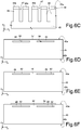
- a wafer 45 of semiconductor material in particular monocrystalline silicon, is provided, having a front surface 45a and a rear surface 45b.
- the manufacturing process then envisages formation of a buried cavity completely contained inside the wafer 45, overlaid by a membrane, with techniques described in detail, for example, in EP 1 324 382 B1 filed in the name of the present Applicant.
- an element of semiconductor material, in particular of monocrystalline silicon is concurrently defined, which is configured to form, as will be clarified hereinafter, the coupling portion 15' (see Figure 6D ) of the actuator element 15 of the actuation structure 10.
- an etching mask 46 is firstly obtained, for example made of photosensitive material, the so-called photoresist.
- the etching mask defines an etching area, which in the example is approximately rectangular (but it may likewise be circular or generically polygonal), and comprises a plurality of first mask portions 46a, for example hexagonal, which define a lattice of openings, for example a honeycomb lattice.
- the etching area of the etching mask 46 corresponds to the area that will be occupied by the buried cavity and has an extension corresponding to the extension of the membrane that will be formed above the same buried cavity.
- the etching mask 46 has a second mask portion 46b, solid and without openings, where the aforesaid coupling portion 15' will be defined.
- the trenches 47 form an open region having a complex shape (corresponding to the lattice of the etching mask 46) where the columns 48 (having a section corresponding to the first mask portions 46a) are arranged. At the centre of the aforesaid open region a central portion of semiconductor material remains, corresponding to the aforesaid second mask portion 46b.
- the etching mask 46 is removed, and an epitaxial growth is carried out in a deoxidising environment (typically, in an atmosphere with a high hydrogen concentration, preferably with trichlorosilane - SiHCl 3 ). Consequently, an epitaxial layer grows above the columns 48 and closes the aforesaid open region formed by the trenches 47 at the top.
- a deoxidising environment typically, in an atmosphere with a high hydrogen concentration, preferably with trichlorosilane - SiHCl 3 .
- a step of thermal annealing is then carried out, for example for 30 minutes at 1190°C, preferably in a reducing atmosphere, typically a hydrogen atmosphere.
- the annealing step causes migration of silicon atoms, which tend to move into a position of lower energy. Consequently, and also thanks to the short distance between the columns 48, the silicon atoms completely migrate from the portions of the columns 48 inside the aforesaid open region formed by the trenches 47, and, starting from said region, a buried cavity 50 (as illustrated in Figure 6D , which represents a more extensive portion of the wafer 45) is formed.
- a thin layer of monocrystalline silicon remains above the buried cavity 50, constituted partly by silicon atoms grown epitaxially and partly by migrated silicon atoms and which forms the membrane, designated by 49.
- the membrane 49 is coupled to the coupling portion 15', arranged centrally with respect to the buried cavity 50.
- the manufacturing process then proceeds with oxidation (which may be complete, as in the example illustrated, or even only partial, with formation of an internal coating layer) of the buried cavity 50 so as to form a buried-oxide region 52 underneath the membrane 49 and surrounding the aforesaid coupling portion 15'.
- the above oxidation step envisages carrying out an etch starting from the top surface 45a of the wafer 45 through appropriate masking so as to form access trenches, which extend through the membrane 49 and reach the buried cavity 50.
- a step of thermal oxidation of the internal walls of the buried cavity 50 is carried out, supplying oxygen through the access trenches; the oxide grows progressively starting from the walls up to complete closing of the access trenches and possibly of the buried cavity 50 (or, alternatively, with formation of the coating layer inside the buried cavity 50).
- the manufacturing process then proceeds with formation, on the front surface 45a of the wafer 45, at the top of the membrane 49, of a piezoelectric actuation structure 54, including piezoelectric material.
- the piezoelectric actuation structure 54 may be formed by a stack of layers superimposed on one another, for example made by the superposition of a bottom dielectric layer, of a first electrode layer, of a piezoelectric layer, of a second electrode layer, and of a top dielectric layer.
- a passivation layer is formed on the piezoelectric actuation structure 54 (once again designated by 20, as in the case discussed previously with regard to Figure 2 ).
- the passivation layer 20 and the underlying piezoelectric actuation structure 54 are then etched by means of an appropriate masking so as to form the contact openings 23 towards the piezoelectric actuation structure 54.
- these contact openings are filled by conductive material in a step of formation of electrical-connection paths 22 on the passivation layer 20, as illustrated in Figure 6H .
- the piezoelectric actuation structure 54 and the underlying membrane 49 are subjected to etching by means of an appropriate masking, for definition of the geometry of the cantilever elements 18 and of the overlying piezoelectric regions 19 of the actuation structure 10.
- the elastic coupling elements 17 may be formed (which are illustrated schematically only in the aforesaid Figure 6L ), which connect the cantilever elements 18 to the coupling portion 15' of the actuator element 15 of the actuation structure 10.
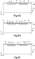
- the wafer 45 is flipped and, on the rear surface 45b of the wafer 45, oxide regions 58 are formed in a position vertically corresponding to the coupling portion 15' (inner oxide region 58a) and externally with respect to the position assumed by the cantilever elements 18 on the front surface 45a (outer oxide region 58b); in particular, the outer and inner oxide regions 58b, 58a are separated along the direction of longitudinal extension of the cantilever elements 18 by the third width L3.
- Mask regions 59 are then formed on the oxide regions 58, and in particular an inner mask region 59a that covers the inner oxide region 58a and an outer mask region 59b that covers the outer oxide region 58b; the outer and inner mask regions 59b, 59a are separated along the aforesaid direction of longitudinal extension of the cantilever elements 18 by the second width L2.
- a first etch of the wafer 45 is carried out, starting from the rear surface 45b, through the mask regions 59, to form deep cavities 60 (having the aforesaid second width L2), which extend vertically in the wafer 45, starting from the aforesaid rear surface 45b until they reach the buried-oxide region 52.
- the mask regions 59 are then removed, and a further etch of the wafer 45 is carried out, Figure 6K , once again starting from the rear surface 45b, this time through the oxide regions 58 to form surface cavities 61 (having the aforesaid third width L3), which extend in a surface portion of the wafer 45 at the aforesaid rear surface 45b.
- the aforesaid etching steps carried out in succession hence lead (concurrently, i.e., without any need for further and distinct processing steps) to formation of the second stopper arrangement 32, and in particular of the second stopper surface 32'.
- the geometrical characteristics of the mask regions 59 and of the oxide regions 58 and the characteristics of the etching determine the dimensional characteristics of the aforesaid second stopper arrangement 32 and in particular the extension of the second stopper surface 32' and the distance of the second stopper surface 32' from the rear surface 45b (i.e., the distance d2).
- the recess that is defined in the actuator element 15 at the rear surface 45b of the wafer 45 limits adhesion of the actuator element 15 to adhesive tape during the subsequent processing steps (any possible mechanical failure of the cantilever elements 18 during detachment of the wafer 45 from the tape during the assembly steps is thus reduced).
- the removal of the buried oxide also leads (concurrently, i.e., without any need for further and distinct processing steps) to definition of the first stopper arrangement 30, and in particular of the first stopper surface 30' facing the cantilever elements 18.
- the geometrical characteristics of the mask regions 59 (illustrated in the aforesaid Figure 6J ) and the geometrical characteristics of the buried cavity 50 determine in this case the dimensional characteristics of the aforesaid first stopper arrangement 30 and in particular the extension of the first stopper surface 30' and the distance d1 of the first stopper surface 30' from the cantilever elements 18.
- the process then end (in a way not illustrated) with dicing of the wafer 45 for definition of a plurality of dies 12, each comprising, in the same monolithic body 13, the frame 14, the actuator element 15, and the aforesaid cantilever elements 18, interposed between the frame 14 and the actuator element 15.
- the actuation structure 10 of the MEMS electroacoustic transducer 11 includes bi-directional stopper elements, i.e., acting in both directions of the vertical axis z, enabling, in the case of impact or dropping, effective limitation of damage both to the acoustic membrane 35 and to the cantilever elements 18 and the overlying piezoelectric regions 19.
- the first and the second stopper arrangements 30, 32 are integrated and defined in the die 12, in which the actuation structure 10 is obtained, without couplings with external structures being required; simple manufacturing and reduced dimensions are thus achieved.
- the dimensional characteristics of the stopper arrangements 30, 32 are a direct consequence of the manufacturing process for producing the actuation structure 10, being thus easy to vary the extension of the facing surface and the facing distance, in particular between the first stopper surface 30' and the facing cantilever elements 18, and between the second stopper surface 32' and the facing rigid lamina 34 (as highlighted schematically by the dashed rectangles and by the arrows in Figure 2 ).
- the cantilever elements 18, being made of monocrystalline silicon, are stress-free.
- the structure and the process described guarantee a considerable freedom of design in the manufacturing of the cantilever elements 18, in particular with the aim of obtaining a structure that, by maximising displacement of the actuator element 15 connected to the acoustic membrane 35, maximises the sound power level thereof (dB SPL) as compared to known solutions.
- the MEMS electroacoustic transducer 11 is advantageously protected from contamination, in effect being resistant to liquids (waterproof) and dust (dustproof), being developed with piezoelectric technology.
- Figures 7A-7D are schematic illustrations of possible alternative embodiments, in which in particular: the cantilever elements 18 are once again four in number and are elastically coupled to the actuator element 15 by means of respective elastic coupling elements or coupling springs 17, having, however, in this case a generically trapezoidal shape ( Figure 7A ); the cantilever elements 18 are once again four in number and have a generically triangular shape, being connected directly and integrally to the coupling element 15, i.e., without the presence of elastic coupling elements ( Figure 7B ) - also in this case, the elastic elements could in any case be present; the cantilever elements 18 are two in number, are elastically coupled to the actuator element 15 by means of respective elastic coupling elements 17 and have a generically circular half-ring shape ( Figure 7C ); the cantilever elements 18 are four in number, are elastically coupled to the actuator element 15 by means of respective elastic coupling elements 17, have a generically rectangular shape, and are carried by a same external structure 63 with a circular-ring conformation
- the piezoelectric regions 19 may extend also above the actuator element 15, or else be removed from the front surface 13a of the monolithic body 13 at the same actuator element 15.
- the piezoelectric regions 19 may also be of a bi-morphic type, i.e., including a double layer of piezoelectric material, each layer being interposed between two electrodes.
- the MEMS electroacoustic transducer 11 may further comprise an ASIC (Application-Specific Integrated Circuit), coupled to the actuation structure 10, for example to provide electrical biasing signals.
- ASIC Application-Specific Integrated Circuit
- This ASIC electronic circuit can be integrated in the same die 12 where the actuation structure 10 is made, or may be obtained in a distinct die of semiconductor material, which can be housed in the same package as that of the aforesaid die 12.
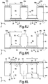
- an alternative manufacturing process may envisage different initial steps for providing the buried-oxide region 52 underneath the front surface 45a of the wafer 45.
- the process may in this case envisage providing a SOI (Silicon-On-Insulator) wafer, once again designated by 45, having an active layer 66, for example made of monocrystalline silicon, an insulating layer 67, for example made of silicon oxide, and a supporting layer 68, for example once again made of monocrystalline silicon.
- SOI Silicon-On-Insulator
- the active layer 66 (after being possibly subjected to a surface thinning-out process) and the insulating layer 67 are subjected to etching so as to define a stacked region 69 of portions of the same active layer 66 and of the insulating layer 67, having an extension corresponding to what will become the central opening 16 and having, at the centre, an opening corresponding to what will become the arrangement of the coupling portion 15' of the actuator element 15.
- FIG. 8B the front surface of the wafer is subjected to re-growth of silicon and planarization so as to cause formation, starting from the aforesaid stacked region 69, of the buried-oxide region 52, the membrane 49, over the buried-oxide region 52, and the aforesaid coupling portion 15' of the actuator element 15.
- a monolithic body of monocrystalline silicon is hence formed, in a way altogether similar to what has been described previously.
- the manufacturing process may then proceed in a way altogether similar to what has been discussed previously (in particular, starting from Figure 6F ).
- the MEMS electroacoustic transducer 11 may act so as to detect sound waves; i.e., it may provide a MEMS microphone sensor (instead of a MEMS speaker, which has been described previously).
Landscapes
- Engineering & Computer Science (AREA)
- Physics & Mathematics (AREA)
- Acoustics & Sound (AREA)
- Signal Processing (AREA)
- Manufacturing & Machinery (AREA)
- Microelectronics & Electronic Packaging (AREA)
- Computer Hardware Design (AREA)
- Micromachines (AREA)
- Piezo-Electric Transducers For Audible Bands (AREA)
Claims (21)
- Betätigungsstruktur (10) eines elektroakustischen MEMS Wandlers (11), umfassend eine Form (12) aus Halbleitermaterial, die einen monolithischen Körper (13) mit einer vorderen Oberfläche (13a) und einer hinteren Oberfläche (13b) aufweist, der sich in einer horizontalen Ebene (xy) erstreckt und Folgendes umfasst: einen Rahmen (14); ein Betätigungselement (15), das in einer mittleren Öffnung (16), die durch den Rahmen (14) definiert ist, angeordnet ist; Auslegerelemente (18), die an der vorderen Oberfläche (13a) zwischen dem Betätigungselement (15) und dem Rahmen (14) gekoppelt sind; und piezoelektrische Regionen (19), die an den Auslegerelementen (18) angeordnet sind und konfiguriert sind, um vorgespannt zu werden, um eine Verformung der Auslegerelemente (18) durch piezoelektrischen Effekt zu bewirken,
dadurch gekennzeichnet, dass sie eine erste Stopperanordnung (30) umfasst, die in der Form (12) integriert ist und konfiguriert ist, um mit den Auslegerelementen (18) zusammenzuwirken, um eine Bewegung davon in einer ersten Richtung einer vertikalen Achse (z) orthogonal zur horizontalen Ebene (xy) zur zugrundeliegenden mittleren Öffnung (16) zu begrenzen. - Struktur nach Anspruch 1, wobei der Rahmen (14) eine Wand aufweist, die der mittleren Öffnung (16) zugewandt ist, und sich entlang der vertikalen Achse (z) erstreckt, und die erste Stopperanordnung (30) erste Aussparungen (25a) der Wand des Rahmens (14) an der vorderen Oberfläche (13a) umfasst, die eine erste Stopperoberfläche (30') bestimmen, die den Auslegerelementen (18) zugewandt ist, in einem Ruhezustand in Abwesenheit einer Verformung der Auslegerelemente (18) durch den piezoelektrischen Effekt in einem ersten Abstand (d1) in Bezug auf die Auslegerelemente (18) angeordnet.
- Struktur nach Anspruch 2, wobei das Betätigungselement (15) eine jeweilige Wand aufweist, die der mittleren Öffnung (16) zugewandt ist und sich entlang der vertikalen Achse (z) erstreckt, und die erste Stopperanordnung (30) jeweilige erste Aussparungen (26a) der Wand des Betätigungselements (15) an der vorderen Oberfläche (13a) umfasst, die eine jeweilige Stopperoberfläche (30') bestimmen, die den Auslegerelementen (18) zugewandt ist.
- Struktur nach einem der vorstehenden Ansprüche, weiter eine zweite Stopperanordnung (32) umfassend, die ebenfalls in der Form (12) integriert ist, und konfiguriert ist, um eine Bewegung der Auslegerelemente (18) in einer zweiten Richtung der vertikalen Achse (z) zu begrenzen, die sich von der zugrundeliegenden mittleren Öffnung (16) wegbewegt; wobei die erste (30) und zweite (32) Stopperanordnung gemeinsam einen bidirektionalen Stoppermechanismus entlang der vertikalen Achse (z) für die Betätigungsstruktur (10) definieren.
- Struktur nach Anspruch 4, wobei der Rahmen (14) eine Wand aufweist, die der mittleren Öffnung (16) zugewandt ist, und sich entlang der vertikalen Achse (z) erstreckt, und die zweite Stopperanordnung (32) zweite Aussparungen (25b) der Wand des Rahmens (14) an der hinteren Oberfläche (13b) umfasst, die eine zweite Stopperoberfläche (32') bestimmen, die in einem zweiten Abstand (d2) in Bezug auf die hintere Oberfläche (13b) angeordnet ist.
- Struktur nach Anspruch 5, wobei das Betätigungselement (15) eine jeweilige Wand aufweist, die der mittleren Öffnung (16) zugewandt ist und sich entlang der vertikalen Achse (z) erstreckt, und die zweite Stopperanordnung (32) jeweilige zweite Aussparungen (26b) der Wand des Betätigungselements (15) an der hinteren Oberfläche (13b) umfasst, die eine jeweilige Stopperoberfläche (32') bestimmen.
- Struktur nach einem der vorstehenden Ansprüche, wobei die mittlere Öffnung (16) Folgendes beinhaltet: einen ersten Hohlraum (50) an der vorderen Oberfläche (13a), der den Auslegerelementen (18) zugrunde liegt und eine erste Breite (L1) in einer Längsrichtung einer Erstreckung der Auslegerelemente (18) entlang einer horizontalen Achse (x) der horizontalen Ebene (xy) aufweist; einen zweiten Hohlraum (60), der dem ersten Hohlraum (50) zugrunde liegt, und eine zweite Breite (L2) in der Längsrichtung aufweist; und einen dritten Hohlraum (61) an der hinteren Oberfläche (13b), der dem zweiten Hohlraum (60) zugrunde liegt und eine dritte Breite (L3) in der Längsrichtung aufweist; wobei die erste Breite (L1) und die dritte Breite (L3) größer als die zweite Breite (L2) sind.
- Struktur nach einem der vorstehenden Ansprüche, wobei die Auslegerelemente (18) ein erstes Ende aufweisen, das an den Rahmen (14) gekoppelt ist und ein zweites Ende, das durch jeweilige elastische Kopplungselemente (17) elastisch an einen Kopplungsabschnitt (15') des Betätigungselements (15) gekoppelt ist.
- Struktur nach einem der vorstehenden Ansprüche, wobei die Auslegerelemente (18) aus einkristalligem Silizium gefertigt sind.
- Elektroakustischer MEMS Wandler (11), umfassend eine Betätigungsstruktur (10) nach einem der vorstehenden Ansprüche, und eine akustische Membran (35), die mittig an das Betätigungselement (15) gekoppelt ist; wobei eine Verformung der Auslegerelemente (18) durch piezoelektrischen Effekt konfiguriert ist, um eine Verschiebung des Betätigungselements (15) und eine entsprechende Verschiebung der akustischen Membran (35) zu bestimmen.
- Wandler nach Anspruch 10, weiter ein starres Stopperelement (34) umfassend, das zwischen der akustischen Membran (35) und dem Betätigungselement (15) an der hinteren Oberfläche eingesetzt ist.
- Wandler nach Anspruch 10 oder 11, wobei die akustische Membran (35) Endabschnitte aufweist, die an Trägerelemente (36) gekoppelt sind, die an der hinteren Oberfläche (13b) des monolithischen Körpers (13) an den Rahmen (14) gekoppelt sind.
- Wandler nach Anspruch 10 oder 11, weiter eine Gehäusestruktur (40) umfassend, die Folgendes aufweist: einen Sockel (41), an den die Betätigungsstruktur (10) an der vorderen Oberfläche (13a) gekoppelt ist; und einen Trägerabschnitt (42), der die Betätigungsstruktur (10) umgibt, und eine erste Oberfläche aufweist, die an den Sockel (41) gekoppelt ist, und eine zweite Oberfläche, vertikal gegenüber der ersten Oberfläche, an die Endabschnitte der akustischen Membran (35) gekoppelt sind.
- Wandler nach einem der Ansprüche 10 bis 13, der einen Lautsprecher zum Erzeugen von Schallwellen im Audioband definiert.
- Verfahren zur Herstellung einer Betätigungsstruktur (10) eines elektroakustischen MEMS Wandlers (11), umfassend eine Form (12) aus Halbleitermaterial, die einen monolithischen Körper (13) mit einer vorderen Oberfläche (13a) und einer hinteren Oberfläche (13b) aufweist, der sich in einer horizontalen Ebene (xy) erstreckt: einen Rahmen (14); ein Betätigungselement (15), das in einer mittleren Öffnung (16), die durch den Rahmen (14) definiert ist, angeordnet ist; Auslegerelemente (18), die an der vorderen Oberfläche (13a) zwischen dem Betätigungselement (15) und dem Rahmen (14) gekoppelt sind; und piezoelektrische Regionen (19), die an den Auslegerelementen (18) angeordnet sind und konfiguriert sind, um vorgespannt zu werden, um eine Verformung der Auslegerelemente (18) durch piezoelektrischen Effekt zu bewirken,
dadurch gekennzeichnet, dass es das Integrieren einer ersten Stopperanordnung (30) in der Form (12) umfasst, die dazu bestimmt ist, mit den Auslegerelementen (18) zusammenzuwirken, um eine Bewegung davon in einer ersten Richtung einer vertikalen Achse (z) orthogonal zur horizontalen Ebene (xy) zur zugrundeliegenden mittleren Öffnung (16) zu begrenzen. - Verfahren nach Anspruch 15, wobei das Integrieren Folgendes umfasst:Bereitstellen eines Wafers (45) aus Halbleitermaterial, der eine vordere Oberfläche (45a) und eine hintere Oberfläche (45b) aufweist;Bilden einer vergrabenen Oxidregion (52), die von der vorderen Oberfläche (45a) durch eine Membran (49) getrennt ist und eine erste Breite (L1) entlang einer ersten horizontalen Achse (x) der horizontalen Ebene (xy) aufweist;Bilden einer piezoelektrischen Struktur (54) auf der Membran (49);Ätzen der piezoelektrischen Struktur (54) und der Membran (49) zum Definieren der Auslegerelemente (18) und der piezoelektrischen Regionen (19);nacheinander Ätzen des Wafers (45), von der hinteren Oberfläche (45b) beginnend, mit einer ersten Ätzung zur Bildung eines tiefen Hohlraumes (60), der die vergrabene Oxidregion (52) erreicht und eine zweite Breite (L2) aufweist, und anschließend mit einer zweiten Ätzung zur Bildung eines Oberflächenhohlraumes (61) an der hinteren Oberfläche (45b), die eine dritte Breite (L3) aufweist, wobei die erste (L1) und die dritte (L3) Breite größer als die zweite Breite (L2) sind; undEntfernen des Siliziumoxids von der vergrabenen Oxidregion (52), um einen vergrabenen Hohlraum (50) zu definieren, und die Auslegerelemente (18) oberhalb des vergrabenen Hohlraums (50) freizulegen.
- Verfahren nach Anspruch 16, wobei das Entfernen ein gleichzeitiges Definieren in dem Wafer (45) der ersten Stopperanordnung (30) umfasst.
- Verfahren nach Anspruch 16 oder 17, wobei aufeinanderfolgendes Ätzen gleichzeitiges Definieren in dem Wafer (45) einer zweiten Stopperanordnung (32) umfasst, die konfiguriert ist, um eine Bewegung der Auslegerelemente (18) in einer zweiten Richtung der vertikalen Achse (z) von der zugrunde liegenden mittleren Öffnung (16) weg zu begrenzen; wobei die erste (30) und zweite (32) Stopperanordnung gemeinsam einen bidirektionalen Stoppermechanismus entlang der vertikalen Achse (z) für die Betätigungsstruktur (10) definieren.
- Verfahren nach einem der Ansprüche 16 bis 18, wobei das Bilden einer vergrabenen Oxidregion (52) Folgendes umfasst:
Bilden des vergrabenen Hohlraumes (50), der in dem Wafer (45) enthalten ist und durch die Membran (49) von der vorderen Oberfläche (45a) getrennt ist, einen Kopplungsabschnitt (15') aus einem Halbleitermaterial, der in Bezug auf den vergrabenen Hohlraum (50) mittig angeordnet ist und an die Membran (49) gekoppelt ist; und Bilden von Siliziumoxid in dem vergrabenen Hohlraum (50) zur Bildung der vergrabenen Oxidregion (52). - Verfahren nach Anspruch 19, wobei das Bilden eines vergrabenen Hohlraumes (50) Folgendes umfasst:Graben innerhalb des Wafers (45), von der vorderen Oberfläche (45a) beginnend, von Gräben (47), die zwischen sich Säulen (48) aus Halbleitermaterial begrenzen;epitaktisches Wachsen, von den Säulen (48) beginnend, einer Sperrschicht aus Halbleitermaterial, wobei die Sperrschicht die Gräben (47) ganz oben versperrt; undAusführen einer Wärmebehandlung, um eine Migration des Halbleitermaterials der Säulen (48) zur Sperrschicht zu bewirken, um den vergrabenen Hohlraum (50) und gleichzeitig die oberhalb des vergrabenen Hohlraumes (50) aufgehängte Membran (49) zu bilden.
- Verfahren nach einem der Ansprüche 16 bis 18, wobei der Wafer ein SOI (Silicon-On-Insulator) Wafer ist, der eine aktive Schicht (66), eine Isolierschicht (67) und eine Trägerschicht (68) aufweist; und wobei das Bilden einer vergrabenen Oxidregion (52) Folgendes umfasst:Ätzen der aktiven Schicht (66) und der Isolierschicht (67), um eine gestapelte Region (69) von Abschnitten der aktiven Schicht (66) und der Isolierschicht (67) zu definieren; undUnterwerfen der vorderen Oberfläche (45a) des Wafers (45) einem erneuten Silizium-Wachstum, um von der gestapelten Region (69) beginnend die vergrabene Oxidregion (52) und die Membran (49) auf der vergrabenen Oxidregion (52) zu bilden.
Applications Claiming Priority (1)
| Application Number | Priority Date | Filing Date | Title |
|---|---|---|---|
| IT102019000001017A IT201900001017A1 (it) | 2019-01-23 | 2019-01-23 | Trasduttore elettroacustico microelettromeccanico ad attuazione piezoelettrica e relativo procedimento di fabbricazione |
Publications (2)
| Publication Number | Publication Date |
|---|---|
| EP3687192A1 EP3687192A1 (de) | 2020-07-29 |
| EP3687192B1 true EP3687192B1 (de) | 2021-06-30 |
Family
ID=66049616
Family Applications (1)
| Application Number | Title | Priority Date | Filing Date |
|---|---|---|---|
| EP20153473.2A Active EP3687192B1 (de) | 2019-01-23 | 2020-01-23 | Mikroelektromechanischer elektroakustischer wandler mit piezoelektrischer betätigung und entsprechendes herstellungsverfahren |
Country Status (3)
| Country | Link |
|---|---|
| US (1) | US11418888B2 (de) |
| EP (1) | EP3687192B1 (de) |
| IT (1) | IT201900001017A1 (de) |
Families Citing this family (20)
| Publication number | Priority date | Publication date | Assignee | Title |
|---|---|---|---|---|
| IT201900001017A1 (it) * | 2019-01-23 | 2020-07-23 | St Microelectronics Srl | Trasduttore elettroacustico microelettromeccanico ad attuazione piezoelettrica e relativo procedimento di fabbricazione |
| JP6652670B1 (ja) * | 2019-03-14 | 2020-02-26 | 株式会社フジクラ | フィルタ装置 |
| US11252511B2 (en) * | 2019-12-27 | 2022-02-15 | xMEMS Labs, Inc. | Package structure and methods of manufacturing sound producing chip, forming package structure and forming sound producing apparatus |
| US11395073B2 (en) | 2020-04-18 | 2022-07-19 | xMEMS Labs, Inc. | Sound producing package structure and method for packaging sound producing package structure |
| US11057716B1 (en) * | 2019-12-27 | 2021-07-06 | xMEMS Labs, Inc. | Sound producing device |
| IT202000015073A1 (it) * | 2020-06-23 | 2021-12-23 | St Microelectronics Srl | Trasduttore microelettromeccanico a membrana con smorzatore attivo |
| CN113839582B (zh) * | 2020-06-23 | 2025-07-01 | 意法半导体股份有限公司 | 具有有源阻尼器的微机电膜换能器 |
| TWI834968B (zh) * | 2020-10-08 | 2024-03-11 | 阿比特電子科技股份有限公司 | 微機電系統聲學感測器、微機電系統封裝結構及其製造方法 |
| CN113135548B (zh) * | 2021-04-20 | 2024-06-11 | 广州蜂鸟传感科技有限公司 | 一种压电微机械执行器 |
| US12497286B2 (en) * | 2021-07-09 | 2025-12-16 | Frore Systems Inc. | Anchor and cavity configuration for MEMS-based cooling systems |
| US12581620B2 (en) | 2021-07-12 | 2026-03-17 | Frore Systems Inc. | Exit channel configuration for MEMS-based actuator systems |
| US12552660B2 (en) * | 2021-10-26 | 2026-02-17 | Stmicroelectronics S.R.L. | Micro-electro-mechanical device for transducing high-frequency acoustic waves in a propagation medium and manufacturing process thereof |
| EP4447488A4 (de) * | 2021-12-29 | 2025-02-26 | Huawei Technologies Co., Ltd. | Piezoelektrische sensoreinheit, piezoelektrisches mikrofon und endgerät |
| US20230290663A1 (en) * | 2022-03-11 | 2023-09-14 | X-Celeprint Limited | Printing components suspended by frames |
| DE102022205608A1 (de) | 2022-06-01 | 2023-12-07 | Robert Bosch Gesellschaft mit beschränkter Haftung | MEMS-Element zur Bewegung eines Masseelements eines Schallwandlers zum Erzeugen und/oder Empfangen von Schallsignalen sowie ein Schallwandler mit solche einem MEMS-Element |
| EP4297433B1 (de) * | 2022-06-24 | 2026-03-04 | Robert Bosch GmbH | Mikroelektromechanische akustische druckerzeugungsvorrichtung mit verbessertem antrieb |
| SE546765C2 (en) * | 2023-11-06 | 2025-02-18 | Myvox Ab | A micro-electromechanical-system based sound producing device |
| CN120711330A (zh) * | 2024-03-26 | 2025-09-26 | 三美电机株式会社 | 膜片以及电声转换装置 |
| CN120711331A (zh) * | 2024-03-26 | 2025-09-26 | 三美电机株式会社 | Mems设备以及电声转换装置 |
| DE102024205334A1 (de) | 2024-06-10 | 2025-12-11 | Robert Bosch Gesellschaft mit beschränkter Haftung | MEMS-Schallwandler |
Family Cites Families (11)
| Publication number | Priority date | Publication date | Assignee | Title |
|---|---|---|---|---|
| DE60127148T2 (de) | 2001-12-28 | 2007-12-13 | Stmicroelectronics S.R.L., Agrate Brianza | Herstellungsverfahren für SOI Scheibe durch Wärmebehandlung und Oxidation von vergrabenen Kanälen |
| US6654316B1 (en) * | 2002-05-03 | 2003-11-25 | John L. Butler | Single-sided electro-mechanical transduction apparatus |
| JP2008030182A (ja) * | 2006-08-01 | 2008-02-14 | National Institute Of Advanced Industrial & Technology | 定振幅機構及びこれを用いた電位センサ |
| US9510103B2 (en) * | 2013-09-09 | 2016-11-29 | Audio Pixels Ltd. | Microelectromechanical apparatus for generating a physical effect |
| DE102014106753B4 (de) | 2014-05-14 | 2022-08-11 | USound GmbH | MEMS-Lautsprecher mit Aktuatorstruktur und davon beabstandeter Membran |
| DE102014217798A1 (de) * | 2014-09-05 | 2016-03-10 | Fraunhofer-Gesellschaft zur Förderung der angewandten Forschung e.V. | Mikromechanische piezoelektrische Aktuatoren zur Realisierung hoher Kräfte und Auslenkungen |
| DE102015116707A1 (de) * | 2015-10-01 | 2017-04-06 | USound GmbH | Flexible MEMS-Leiterplatteneinheit sowie Schallwandleranordnung |
| US20180152792A1 (en) * | 2016-11-29 | 2018-05-31 | Cirrus Logic International Semiconductor Ltd. | Mems device |
| CN108569672B (zh) * | 2017-03-13 | 2020-08-25 | 中芯国际集成电路制造(上海)有限公司 | 麦克风及其制造方法 |
| TWI683460B (zh) * | 2018-11-30 | 2020-01-21 | 美律實業股份有限公司 | 揚聲器結構 |
| IT201900001017A1 (it) * | 2019-01-23 | 2020-07-23 | St Microelectronics Srl | Trasduttore elettroacustico microelettromeccanico ad attuazione piezoelettrica e relativo procedimento di fabbricazione |
-
2019
- 2019-01-23 IT IT102019000001017A patent/IT201900001017A1/it unknown
-
2020
- 2020-01-22 US US16/749,579 patent/US11418888B2/en active Active
- 2020-01-23 EP EP20153473.2A patent/EP3687192B1/de active Active
Also Published As
| Publication number | Publication date |
|---|---|
| US11418888B2 (en) | 2022-08-16 |
| US20200236470A1 (en) | 2020-07-23 |
| EP3687192A1 (de) | 2020-07-29 |
| IT201900001017A1 (it) | 2020-07-23 |
Similar Documents
| Publication | Publication Date | Title |
|---|---|---|
| EP3687192B1 (de) | Mikroelektromechanischer elektroakustischer wandler mit piezoelektrischer betätigung und entsprechendes herstellungsverfahren | |
| KR100899482B1 (ko) | 실리콘 마이크 및 그의 제조 방법 | |
| KR101955791B1 (ko) | 콤 드라이브 mems 장치용 시스템 및 방법 | |
| EP3247134B1 (de) | Akustischer mems-wandler mit kammfingerelektroden und zugehöriges herstellungsverfahren | |
| KR101910867B1 (ko) | 차동 콤 드라이브 mems를 위한 시스템 및 방법 | |
| US20090185700A1 (en) | Vibration transducer and manufacturing method therefor | |
| KR20080034407A (ko) | 정전 압력 변환기 및 그 제조 방법 | |
| TWI738804B (zh) | Mems裝置與製程 | |
| JP2009291514A (ja) | 静電容量型トランスデューサの製造方法、及び静電容量型トランスデューサ | |
| TW200532746A (en) | Electronic component, electronic component module and method of manufacturing the electronic component | |
| JP2008546240A (ja) | シリコンマイクロフォン | |
| JP2012529207A (ja) | マイクロメカニカルマイクロフォン構造体を有する素子、および、マイクロメカニカルマイクロフォン構造体を有する素子の製造方法 | |
| KR101764314B1 (ko) | 음향 센서 및 그 제조 방법 | |
| US12302063B2 (en) | Acoustic device with connected cantilever | |
| US12509345B2 (en) | Microelectromechanical acoustic pressure-generating device with improved drive | |
| JP5721452B2 (ja) | 静電容量型memsセンサ | |
| CN110881163B (zh) | Mems换能器和用于制造mems换能器的方法 | |
| US11402288B2 (en) | Membrane-based sensor having a plurality of spacers extending from a cap layer | |
| JP2008252854A (ja) | 静電型トランスデューサおよびその製造方法 | |
| JP5775281B2 (ja) | Memsセンサおよびその製造方法 | |
| US12139394B2 (en) | Multiple layer electrode transducers | |
| JP4944494B2 (ja) | 静電容量型センサ | |
| KR102942649B1 (ko) | 패키지 구조체, 장치 및 그 형성 방법 | |
| CN120730232B (zh) | 一种三维定位压电mems麦克风及其制备方法 |
Legal Events
| Date | Code | Title | Description |
|---|---|---|---|
| PUAI | Public reference made under article 153(3) epc to a published international application that has entered the european phase |
Free format text: ORIGINAL CODE: 0009012 |
|
| STAA | Information on the status of an ep patent application or granted ep patent |
Free format text: STATUS: THE APPLICATION HAS BEEN PUBLISHED |
|
| AK | Designated contracting states |
Kind code of ref document: A1 Designated state(s): AL AT BE BG CH CY CZ DE DK EE ES FI FR GB GR HR HU IE IS IT LI LT LU LV MC MK MT NL NO PL PT RO RS SE SI SK SM TR |
|
| AX | Request for extension of the european patent |
Extension state: BA ME |
|
| STAA | Information on the status of an ep patent application or granted ep patent |
Free format text: STATUS: REQUEST FOR EXAMINATION WAS MADE |
|
| 17P | Request for examination filed |
Effective date: 20201201 |
|
| RBV | Designated contracting states (corrected) |
Designated state(s): AL AT BE BG CH CY CZ DE DK EE ES FI FR GB GR HR HU IE IS IT LI LT LU LV MC MK MT NL NO PL PT RO RS SE SI SK SM TR |
|
| GRAP | Despatch of communication of intention to grant a patent |
Free format text: ORIGINAL CODE: EPIDOSNIGR1 |
|
| STAA | Information on the status of an ep patent application or granted ep patent |
Free format text: STATUS: GRANT OF PATENT IS INTENDED |
|
| RIC1 | Information provided on ipc code assigned before grant |
Ipc: H04R 19/00 20060101AFI20201223BHEP |
|
| INTG | Intention to grant announced |
Effective date: 20210122 |
|
| GRAS | Grant fee paid |
Free format text: ORIGINAL CODE: EPIDOSNIGR3 |
|
| GRAA | (expected) grant |
Free format text: ORIGINAL CODE: 0009210 |
|
| STAA | Information on the status of an ep patent application or granted ep patent |
Free format text: STATUS: THE PATENT HAS BEEN GRANTED |
|
| AK | Designated contracting states |
Kind code of ref document: B1 Designated state(s): AL AT BE BG CH CY CZ DE DK EE ES FI FR GB GR HR HU IE IS IT LI LT LU LV MC MK MT NL NO PL PT RO RS SE SI SK SM TR |
|
| REG | Reference to a national code |
Ref country code: CH Ref legal event code: EP |
|
| REG | Reference to a national code |
Ref country code: AT Ref legal event code: REF Ref document number: 1407513 Country of ref document: AT Kind code of ref document: T Effective date: 20210715 |
|
| REG | Reference to a national code |
Ref country code: DE Ref legal event code: R096 Ref document number: 602020000195 Country of ref document: DE |
|
| REG | Reference to a national code |
Ref country code: IE Ref legal event code: FG4D |
|
| REG | Reference to a national code |
Ref country code: LT Ref legal event code: MG9D |
|
| PG25 | Lapsed in a contracting state [announced via postgrant information from national office to epo] |
Ref country code: HR Free format text: LAPSE BECAUSE OF FAILURE TO SUBMIT A TRANSLATION OF THE DESCRIPTION OR TO PAY THE FEE WITHIN THE PRESCRIBED TIME-LIMIT Effective date: 20210630 Ref country code: FI Free format text: LAPSE BECAUSE OF FAILURE TO SUBMIT A TRANSLATION OF THE DESCRIPTION OR TO PAY THE FEE WITHIN THE PRESCRIBED TIME-LIMIT Effective date: 20210630 Ref country code: BG Free format text: LAPSE BECAUSE OF FAILURE TO SUBMIT A TRANSLATION OF THE DESCRIPTION OR TO PAY THE FEE WITHIN THE PRESCRIBED TIME-LIMIT Effective date: 20210930 |
|
| REG | Reference to a national code |
Ref country code: NL Ref legal event code: MP Effective date: 20210630 |
|
| REG | Reference to a national code |
Ref country code: AT Ref legal event code: MK05 Ref document number: 1407513 Country of ref document: AT Kind code of ref document: T Effective date: 20210630 |
|
| PG25 | Lapsed in a contracting state [announced via postgrant information from national office to epo] |
Ref country code: SE Free format text: LAPSE BECAUSE OF FAILURE TO SUBMIT A TRANSLATION OF THE DESCRIPTION OR TO PAY THE FEE WITHIN THE PRESCRIBED TIME-LIMIT Effective date: 20210630 Ref country code: RS Free format text: LAPSE BECAUSE OF FAILURE TO SUBMIT A TRANSLATION OF THE DESCRIPTION OR TO PAY THE FEE WITHIN THE PRESCRIBED TIME-LIMIT Effective date: 20210630 Ref country code: NO Free format text: LAPSE BECAUSE OF FAILURE TO SUBMIT A TRANSLATION OF THE DESCRIPTION OR TO PAY THE FEE WITHIN THE PRESCRIBED TIME-LIMIT Effective date: 20210930 Ref country code: LV Free format text: LAPSE BECAUSE OF FAILURE TO SUBMIT A TRANSLATION OF THE DESCRIPTION OR TO PAY THE FEE WITHIN THE PRESCRIBED TIME-LIMIT Effective date: 20210630 Ref country code: GR Free format text: LAPSE BECAUSE OF FAILURE TO SUBMIT A TRANSLATION OF THE DESCRIPTION OR TO PAY THE FEE WITHIN THE PRESCRIBED TIME-LIMIT Effective date: 20211001 |
|
| PG25 | Lapsed in a contracting state [announced via postgrant information from national office to epo] |
Ref country code: EE Free format text: LAPSE BECAUSE OF FAILURE TO SUBMIT A TRANSLATION OF THE DESCRIPTION OR TO PAY THE FEE WITHIN THE PRESCRIBED TIME-LIMIT Effective date: 20210630 Ref country code: ES Free format text: LAPSE BECAUSE OF FAILURE TO SUBMIT A TRANSLATION OF THE DESCRIPTION OR TO PAY THE FEE WITHIN THE PRESCRIBED TIME-LIMIT Effective date: 20210630 Ref country code: SK Free format text: LAPSE BECAUSE OF FAILURE TO SUBMIT A TRANSLATION OF THE DESCRIPTION OR TO PAY THE FEE WITHIN THE PRESCRIBED TIME-LIMIT Effective date: 20210630 Ref country code: CZ Free format text: LAPSE BECAUSE OF FAILURE TO SUBMIT A TRANSLATION OF THE DESCRIPTION OR TO PAY THE FEE WITHIN THE PRESCRIBED TIME-LIMIT Effective date: 20210630 Ref country code: AT Free format text: LAPSE BECAUSE OF FAILURE TO SUBMIT A TRANSLATION OF THE DESCRIPTION OR TO PAY THE FEE WITHIN THE PRESCRIBED TIME-LIMIT Effective date: 20210630 Ref country code: SM Free format text: LAPSE BECAUSE OF FAILURE TO SUBMIT A TRANSLATION OF THE DESCRIPTION OR TO PAY THE FEE WITHIN THE PRESCRIBED TIME-LIMIT Effective date: 20210630 Ref country code: PT Free format text: LAPSE BECAUSE OF FAILURE TO SUBMIT A TRANSLATION OF THE DESCRIPTION OR TO PAY THE FEE WITHIN THE PRESCRIBED TIME-LIMIT Effective date: 20211102 Ref country code: NL Free format text: LAPSE BECAUSE OF FAILURE TO SUBMIT A TRANSLATION OF THE DESCRIPTION OR TO PAY THE FEE WITHIN THE PRESCRIBED TIME-LIMIT Effective date: 20210630 Ref country code: RO Free format text: LAPSE BECAUSE OF FAILURE TO SUBMIT A TRANSLATION OF THE DESCRIPTION OR TO PAY THE FEE WITHIN THE PRESCRIBED TIME-LIMIT Effective date: 20210630 |
|
| PG25 | Lapsed in a contracting state [announced via postgrant information from national office to epo] |
Ref country code: PL Free format text: LAPSE BECAUSE OF FAILURE TO SUBMIT A TRANSLATION OF THE DESCRIPTION OR TO PAY THE FEE WITHIN THE PRESCRIBED TIME-LIMIT Effective date: 20210630 |
|
| REG | Reference to a national code |
Ref country code: DE Ref legal event code: R097 Ref document number: 602020000195 Country of ref document: DE |
|
| PG25 | Lapsed in a contracting state [announced via postgrant information from national office to epo] |
Ref country code: DK Free format text: LAPSE BECAUSE OF FAILURE TO SUBMIT A TRANSLATION OF THE DESCRIPTION OR TO PAY THE FEE WITHIN THE PRESCRIBED TIME-LIMIT Effective date: 20210630 |
|
| PLBE | No opposition filed within time limit |
Free format text: ORIGINAL CODE: 0009261 |
|
| STAA | Information on the status of an ep patent application or granted ep patent |
Free format text: STATUS: NO OPPOSITION FILED WITHIN TIME LIMIT |
|
| PG25 | Lapsed in a contracting state [announced via postgrant information from national office to epo] |
Ref country code: AL Free format text: LAPSE BECAUSE OF FAILURE TO SUBMIT A TRANSLATION OF THE DESCRIPTION OR TO PAY THE FEE WITHIN THE PRESCRIBED TIME-LIMIT Effective date: 20210630 |
|
| 26N | No opposition filed |
Effective date: 20220331 |
|
| PG25 | Lapsed in a contracting state [announced via postgrant information from national office to epo] |
Ref country code: IT Free format text: LAPSE BECAUSE OF FAILURE TO SUBMIT A TRANSLATION OF THE DESCRIPTION OR TO PAY THE FEE WITHIN THE PRESCRIBED TIME-LIMIT Effective date: 20210630 |
|
| PG25 | Lapsed in a contracting state [announced via postgrant information from national office to epo] |
Ref country code: MC Free format text: LAPSE BECAUSE OF FAILURE TO SUBMIT A TRANSLATION OF THE DESCRIPTION OR TO PAY THE FEE WITHIN THE PRESCRIBED TIME-LIMIT Effective date: 20210630 |
|
| REG | Reference to a national code |
Ref country code: BE Ref legal event code: MM Effective date: 20220131 |
|
| PG25 | Lapsed in a contracting state [announced via postgrant information from national office to epo] |
Ref country code: LU Free format text: LAPSE BECAUSE OF NON-PAYMENT OF DUE FEES Effective date: 20220123 |
|
| PG25 | Lapsed in a contracting state [announced via postgrant information from national office to epo] |
Ref country code: FR Free format text: LAPSE BECAUSE OF NON-PAYMENT OF DUE FEES Effective date: 20220131 Ref country code: BE Free format text: LAPSE BECAUSE OF NON-PAYMENT OF DUE FEES Effective date: 20220131 |
|
| PG25 | Lapsed in a contracting state [announced via postgrant information from national office to epo] |
Ref country code: IE Free format text: LAPSE BECAUSE OF NON-PAYMENT OF DUE FEES Effective date: 20220123 |
|
| PG25 | Lapsed in a contracting state [announced via postgrant information from national office to epo] |
Ref country code: LT Free format text: LAPSE BECAUSE OF FAILURE TO SUBMIT A TRANSLATION OF THE DESCRIPTION OR TO PAY THE FEE WITHIN THE PRESCRIBED TIME-LIMIT Effective date: 20210630 |
|
| REG | Reference to a national code |
Ref country code: CH Ref legal event code: PL |
|
| PG25 | Lapsed in a contracting state [announced via postgrant information from national office to epo] |
Ref country code: LI Free format text: LAPSE BECAUSE OF NON-PAYMENT OF DUE FEES Effective date: 20230131 Ref country code: CH Free format text: LAPSE BECAUSE OF NON-PAYMENT OF DUE FEES Effective date: 20230131 |
|
| PG25 | Lapsed in a contracting state [announced via postgrant information from national office to epo] |
Ref country code: MK Free format text: LAPSE BECAUSE OF FAILURE TO SUBMIT A TRANSLATION OF THE DESCRIPTION OR TO PAY THE FEE WITHIN THE PRESCRIBED TIME-LIMIT Effective date: 20210630 Ref country code: CY Free format text: LAPSE BECAUSE OF FAILURE TO SUBMIT A TRANSLATION OF THE DESCRIPTION OR TO PAY THE FEE WITHIN THE PRESCRIBED TIME-LIMIT Effective date: 20210630 |
|
| PG25 | Lapsed in a contracting state [announced via postgrant information from national office to epo] |
Ref country code: HU Free format text: LAPSE BECAUSE OF FAILURE TO SUBMIT A TRANSLATION OF THE DESCRIPTION OR TO PAY THE FEE WITHIN THE PRESCRIBED TIME-LIMIT; INVALID AB INITIO Effective date: 20200123 |
|
| GBPC | Gb: european patent ceased through non-payment of renewal fee |
Effective date: 20240123 |
|
| PG25 | Lapsed in a contracting state [announced via postgrant information from national office to epo] |
Ref country code: MT Free format text: LAPSE BECAUSE OF FAILURE TO SUBMIT A TRANSLATION OF THE DESCRIPTION OR TO PAY THE FEE WITHIN THE PRESCRIBED TIME-LIMIT Effective date: 20210630 |
|
| PG25 | Lapsed in a contracting state [announced via postgrant information from national office to epo] |
Ref country code: GB Free format text: LAPSE BECAUSE OF NON-PAYMENT OF DUE FEES Effective date: 20240123 |
|
| PG25 | Lapsed in a contracting state [announced via postgrant information from national office to epo] |
Ref country code: GB Free format text: LAPSE BECAUSE OF NON-PAYMENT OF DUE FEES Effective date: 20240123 |
|
| PGFP | Annual fee paid to national office [announced via postgrant information from national office to epo] |
Ref country code: DE Payment date: 20241218 Year of fee payment: 6 |
|
| PG25 | Lapsed in a contracting state [announced via postgrant information from national office to epo] |
Ref country code: TR Free format text: LAPSE BECAUSE OF FAILURE TO SUBMIT A TRANSLATION OF THE DESCRIPTION OR TO PAY THE FEE WITHIN THE PRESCRIBED TIME-LIMIT Effective date: 20210630 |