EP3687064B1 - Digital gesteuerter vektorsignalmodulator - Google Patents
Digital gesteuerter vektorsignalmodulator Download PDFInfo
- Publication number
- EP3687064B1 EP3687064B1 EP19153196.1A EP19153196A EP3687064B1 EP 3687064 B1 EP3687064 B1 EP 3687064B1 EP 19153196 A EP19153196 A EP 19153196A EP 3687064 B1 EP3687064 B1 EP 3687064B1
- Authority
- EP
- European Patent Office
- Prior art keywords
- quadrature
- phase
- switching
- bits
- signal
- Prior art date
- Legal status (The legal status is an assumption and is not a legal conclusion. Google has not performed a legal analysis and makes no representation as to the accuracy of the status listed.)
- Active
Links
Images

Classifications
-
- H—ELECTRICITY
- H04—ELECTRIC COMMUNICATION TECHNIQUE
- H04L—TRANSMISSION OF DIGITAL INFORMATION, e.g. TELEGRAPHIC COMMUNICATION
- H04L27/00—Modulated-carrier systems
- H04L27/18—Phase-modulated carrier systems, i.e. using phase-shift keying
-
- H—ELECTRICITY
- H03—ELECTRONIC CIRCUITRY
- H03F—AMPLIFIERS
- H03F3/00—Amplifiers with only discharge tubes or only semiconductor devices as amplifying elements
- H03F3/45—Differential amplifiers
- H03F3/45071—Differential amplifiers with semiconductor devices only
- H03F3/45076—Differential amplifiers with semiconductor devices only characterised by the way of implementation of the active amplifying circuit in the differential amplifier
- H03F3/45475—Differential amplifiers with semiconductor devices only characterised by the way of implementation of the active amplifying circuit in the differential amplifier using IC blocks as the active amplifying circuit
-
- H—ELECTRICITY
- H03—ELECTRONIC CIRCUITRY
- H03C—MODULATION
- H03C3/00—Angle modulation
- H03C3/38—Angle modulation by converting amplitude modulation to angle modulation
- H03C3/40—Angle modulation by converting amplitude modulation to angle modulation using two signal paths the outputs of which have a predetermined phase difference and at least one output being amplitude-modulated
-
- H—ELECTRICITY
- H03—ELECTRONIC CIRCUITRY
- H03C—MODULATION
- H03C5/00—Amplitude modulation and angle modulation produced simultaneously or at will by the same modulating signal
-
- H—ELECTRICITY
- H03—ELECTRONIC CIRCUITRY
- H03D—DEMODULATION OR TRANSFERENCE OF MODULATION FROM ONE CARRIER TO ANOTHER
- H03D7/00—Transference of modulation from one carrier to another, e.g. frequency-changing
- H03D7/16—Multiple-frequency-changing
- H03D7/165—Multiple-frequency-changing at least two frequency changers being located in different paths, e.g. in two paths with carriers in quadrature
- H03D7/166—Multiple-frequency-changing at least two frequency changers being located in different paths, e.g. in two paths with carriers in quadrature using two or more quadrature frequency translation stages
-
- H—ELECTRICITY
- H03—ELECTRONIC CIRCUITRY
- H03F—AMPLIFIERS
- H03F3/00—Amplifiers with only discharge tubes or only semiconductor devices as amplifying elements
- H03F3/189—High-frequency amplifiers, e.g. radio frequency amplifiers
- H03F3/19—High-frequency amplifiers, e.g. radio frequency amplifiers with semiconductor devices only
- H03F3/195—High-frequency amplifiers, e.g. radio frequency amplifiers with semiconductor devices only in integrated circuits
-
- H—ELECTRICITY
- H03—ELECTRONIC CIRCUITRY
- H03F—AMPLIFIERS
- H03F3/00—Amplifiers with only discharge tubes or only semiconductor devices as amplifying elements
- H03F3/45—Differential amplifiers
- H03F3/45071—Differential amplifiers with semiconductor devices only
-
- H—ELECTRICITY
- H03—ELECTRONIC CIRCUITRY
- H03F—AMPLIFIERS
- H03F3/00—Amplifiers with only discharge tubes or only semiconductor devices as amplifying elements
- H03F3/68—Combinations of amplifiers, e.g. multi-channel amplifiers for stereophonics
-
- H—ELECTRICITY
- H03—ELECTRONIC CIRCUITRY
- H03G—CONTROL OF AMPLIFICATION
- H03G3/00—Gain control in amplifiers or frequency changers
- H03G3/001—Digital control of analog signals
-
- H—ELECTRICITY
- H03—ELECTRONIC CIRCUITRY
- H03G—CONTROL OF AMPLIFICATION
- H03G3/00—Gain control in amplifiers or frequency changers
- H03G3/20—Automatic control
- H03G3/30—Automatic control in amplifiers having semiconductor devices
- H03G3/3052—Automatic control in amplifiers having semiconductor devices in bandpass amplifiers (H.F. or I.F.) or in frequency-changers used in a (super)heterodyne receiver
-
- H—ELECTRICITY
- H04—ELECTRIC COMMUNICATION TECHNIQUE
- H04L—TRANSMISSION OF DIGITAL INFORMATION, e.g. TELEGRAPHIC COMMUNICATION
- H04L27/00—Modulated-carrier systems
- H04L27/18—Phase-modulated carrier systems, i.e. using phase-shift keying
- H04L27/20—Modulator circuits; Transmitter circuits
- H04L27/2032—Modulator circuits; Transmitter circuits for discrete phase modulation, e.g. in which the phase of the carrier is modulated in a nominally instantaneous manner
- H04L27/2053—Modulator circuits; Transmitter circuits for discrete phase modulation, e.g. in which the phase of the carrier is modulated in a nominally instantaneous manner using more than one carrier, e.g. carriers with different phases
- H04L27/206—Modulator circuits; Transmitter circuits for discrete phase modulation, e.g. in which the phase of the carrier is modulated in a nominally instantaneous manner using more than one carrier, e.g. carriers with different phases using a pair of orthogonal carriers, e.g. quadrature carriers
-
- H—ELECTRICITY
- H04—ELECTRIC COMMUNICATION TECHNIQUE
- H04L—TRANSMISSION OF DIGITAL INFORMATION, e.g. TELEGRAPHIC COMMUNICATION
- H04L27/00—Modulated-carrier systems
- H04L27/32—Carrier systems characterised by combinations of two or more of the types covered by groups H04L27/02, H04L27/10, H04L27/18 or H04L27/26
- H04L27/34—Amplitude- and phase-modulated carrier systems, e.g. quadrature-amplitude modulated carrier systems
- H04L27/36—Modulator circuits; Transmitter circuits
- H04L27/362—Modulation using more than one carrier, e.g. with quadrature carriers, separately amplitude modulated
-
- H—ELECTRICITY
- H04—ELECTRIC COMMUNICATION TECHNIQUE
- H04L—TRANSMISSION OF DIGITAL INFORMATION, e.g. TELEGRAPHIC COMMUNICATION
- H04L27/00—Modulated-carrier systems
- H04L27/32—Carrier systems characterised by combinations of two or more of the types covered by groups H04L27/02, H04L27/10, H04L27/18 or H04L27/26
- H04L27/34—Amplitude- and phase-modulated carrier systems, e.g. quadrature-amplitude modulated carrier systems
- H04L27/36—Modulator circuits; Transmitter circuits
- H04L27/365—Modulation using digital generation of the modulated carrier (not including modulation of a digitally generated carrier)
-
- H—ELECTRICITY
- H03—ELECTRONIC CIRCUITRY
- H03F—AMPLIFIERS
- H03F2200/00—Indexing scheme relating to amplifiers
- H03F2200/336—A I/Q, i.e. phase quadrature, modulator or demodulator being used in an amplifying circuit
-
- H—ELECTRICITY
- H03—ELECTRONIC CIRCUITRY
- H03F—AMPLIFIERS
- H03F2200/00—Indexing scheme relating to amplifiers
- H03F2200/421—Multiple switches coupled in the output circuit of an amplifier are controlled by a circuit
-
- H—ELECTRICITY
- H03—ELECTRONIC CIRCUITRY
- H03F—AMPLIFIERS
- H03F2200/00—Indexing scheme relating to amplifiers
- H03F2200/451—Indexing scheme relating to amplifiers the amplifier being a radio frequency amplifier
Definitions
- the present invention relates to a digital-controlled vector signal modulator, and more particularly, to a vector signal modulator directly controlled by digital signal without digital-to-analog signal conversion.
- Electronic systems such as communication systems and test instruments, use vector signal modulators to generate vector signals that meet the amplitude and phase requirement.
- a signal is separated to two signals with different phase degree, i.e., the in-phase (I) and quadrature (Q) signals, first. After then, the amplitudes of the in-phase (I) and quadrature (Q) are modulated, respectively, and finally combined together to generate a vector signal which amplitude and phase both meet requirement.
- the I and Q channels (i.e. signal paths) of the modulator are calibrated to be equal in gain responses, a 45° degree vector signal is generated.
- VGAs variable gain amplifiers
- DACs digital-to-analog converters
- the present invention proposes to realize a vector signal modulator directly from the digital control signal without DACs, saving time and the cost the device considerably.
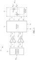
- FIG. 1 is a schematic diagram of a vector modulator 10 according to an embodiment of the present invention.
- the vector modulator 10 comprises a quadrature component generator 12, an in-phase amplifier I-Amp, a quadrature amplifier Q-Amp, a switching circuit 14 and a combining module 16.
- the vector modulator 10 does not include any digital-to-analog converter (DAC).
- the quadrature component generator 12 receives an input radio frequency (RF) signal RF in and generates an input in-phase signal I i and an input quadrature signal Q i according to the RF signal RF in .
- the input in-phase signal I i and the input quadrature signal Q i have 90° phase difference.
- the in-phase amplifier I-Amp receives the input in-phase signal I i and generates an intermediate in-phase signal I m ; the quadrature amplifier Q-Amp receives the input quadrature signal Q i and generates the intermediate quadrature signal Q m .
- the switching circuit 14 comprises a plurality of switches (which will be illustrated later on) and receives a plurality of bits B 1 ,...,B N , where the bits B 1 ,...,B N are configured to control an ON-OFF status of the plurality of switches.
- the switching circuit 14 is configured to adjust the input in-phase signal I i to generate an output in-phase signal I o , and to adjust the input quadrature signal Q j to generate an output quadrature signal Q o , according to the bits B 1 ,...,B N .
- the combining module 16 is configured to combine the output in-phase signal I o and the output quadrature signal Q o to generate an output RF signal RF out .
- the signals RF in , I i , Q i , I m , Q m , I o , Q o and RF out may be voltage signals or current signals.
- the signals RF in , I i , Q i , I m , Q m , I o , Q o and RF out are all differential signals, but not limited thereto. For example, as illustrated in FIG.
- the RF signal RF in /RF out comprises a positive input/output RF signal RF in+ /RF out+ and a negative input/output RF signal RF in- /RF out-
- the input/intermediate/output in-phase signal I i /I m /I o comprises a positive input/intermediate/output in-phase signal I i+ /I m+ /I o+ and a negative input/intermediate/output in-phase signal I j-/ I m- /I o-
- the input/intermediate/output quadrature signal Q i /Q m /Q o comprises a positive input/intermediate/output quadrature signal Q i+ /Q m+ /Q o+ and a negative input/intermediate/output quadrature signal Q i /Q m- /Q o- .
- the in-phase amplifier I-Amp and the quadrature amplifier Q-Amp are full differential amplifiers.
- the in-phase amplifier I-Amp comprises a positive in-phase output terminal O I+ and a negative in-phase output terminal O I- .
- the quadrature amplifier Q-Amp comprises a positive quadrature output terminal O Q+ and a negative quadrature output terminal O Q- .
- the combining module 16 may comprise a first combining element CE+ and a second combining element CE-.
- the first combining element CE+ is configured to generate the positive output RF signal RF out+ by combining the positive output in-phase signal I o+ and the positive output quadrature signal Q o+ .
- the second combining element CE- is configured to generate the negative output RF signal RF out+ by combining the negative output in-phase signal I o- and the negative output quadrature signal Q o- .
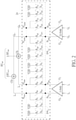
- FIG. 2 is a schematic diagram of a switching circuit 24 according to an embodiment of the present invention.
- the switching circuit 24 is an embodiment of the switching circuit 14.
- the switching circuit 24 comprises a first in-phase switching sub-circuit SW I+ and a first quadrature switching sub-circuit SW Q+ .
- the in-phase switching sub-circuit SW I+ and the quadrature switching sub-circuit SW Q+ have similar circuit structure.
- the first in-phase switching sub-circuit SW I+ comprises a first in-phase switching input terminal N Iin+ , a second in-phase switching input terminal N Iin- , a first in-phase switching output terminal N Iout+ , a second in-phase switching output terminal N Iout- , in-phase conducting switches S I1+ , S I0+ , S I0- , S I1- and in-phase diverting switches S I1+ ', S I0+ ', S I1- ', S I0- '.
- the first in-phase switching input terminal N Iin+ of the in-phase switching sub-circuit SW I+ is coupled to the positive in-phase output terminal O I+ .
- the second in-phase switching input terminal N Iin- of the in-phase switching sub-circuit SW I+ is coupled to the negative in-phase output terminal O I- .
- the in-phase conducting switches S I1+ , S I0+ controlled by in-phase conducting bits B I0 , B I1 , are coupled between the first in-phase switching input terminal N Iin+ and the first in-phase switching output terminal N Iout+ .
- the in-phase conducting switches S I0- , S I1- also controlled by the in-phase conducting bits B I0 , B I1 , are coupled between the second in-phase switching input terminal N Iin- and the second in-phase switching output terminal N Iout- .
- the in-phase diverting switches S I1+ ', S I0+ ', controlled by in-phase diverting bits B I0 ', B I1 ', have one terminal coupled to the first in-phase switching input terminal N Iin+ and have another terminal to receive a voltage VDD.
- the in-phase diverting switches S I1- ', S I0- ', also controlled by the in-phase diverting bits B I0 ', B I1 ', have one terminal coupled to the second in-phase switching input terminal N Iin- and have another terminal to receive the voltage VDD.
- the in-phase diverting bits B I0 ', B I1 ' are complements of the in-phase conducting bits B I0 , B I1 .
- the first quadrature switching sub-circuit SW Q+ comprises a first quadrature switching input terminal N Qin+ , a second quadrature switching input terminal N Qin- , a first quadrature switching output terminal N Qout+ , a second quadrature switching output terminal N Qout- , quadrature conducting switches S Q1+ , S Q0+ , S Q0- , S Q1- and quadrature diverting switches S Q1+ ', S Q0+ ', S Q1- ', S Q0- '.
- the first quadrature switching input terminal N Qin+ of the quadrature switching sub-circuit SW Q+ is coupled to the positive quadrature output terminal O Q+ .
- the second quadrature switching input terminal N Qin- of the quadrature switching sub-circuit SW Q+ is coupled to the negative quadrature output terminal O Q- .
- the quadrature conducting switches S Q1+ , S Q0+ controlled by quadrature conducting bits B Q0 , B Q1 , are coupled between the first quadrature switching input terminal N Qin+ and the first quadrature switching output terminal N Qout+ .
- the quadrature conducting switches S Q0- , S Q1- also controlled by the quadrature conducting bits B Q0 , B Q1 , are coupled between the second quadrature switching input terminal N Qin- and the second quadrature switching output terminal N Qout- .
- the quadrature diverting switches S Q1+ ', S Q0+ ', controlled by quadrature diverting bits B Q0 ', B Q1 ', have one terminal coupled to the first quadrature switching input terminal N Qin+ and have another terminal to receive the voltage VDD.
- the quadrature diverting switches S Q1- ', S Q0- ', also controlled by the quadrature diverting bits B Q0 ', B Q1 ', have one terminal coupled to the second quadrature switching input terminal N Qin- and have another terminal to receive the voltage VDD.
- the conducting bits B I0 , B I1 , B Q0 , B Q1 (or the diverting bits B I0 ', B I1 ', B Q0 ', B Q1 ') of the switching circuit 24 may be regarded as the bits B 1 ,...,B N of the switching circuit 14.
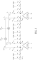
- FIG. 3 is a schematic diagram of a conduction status of the switching circuit 24.
- (B I0 , B I1 , B Q0 , B Q1 ) is (1, 0, 1, 1), which means that the switches S I0+ , S I0- , S I1+ ', S I1- ', S Q1+ , S Q0+ , S Q0- , S Q1- are conducted (ON) and the switches S I1+ , S I1- , S I0+ ', S I0- ' , S Q1+ ', S Q0+ ', S Q1- ', S Q0- ' are cutoff (OFF).
- an output current of the in-phase amplifier I-Amp is denoted as I l and an output current of the quadrature amplifier Q-Amp is denoted as I Q .
- I l an output current of the in-phase amplifier
- I Q an output current of the quadrature amplifier
- I l an output current of the quadrature amplifier
- the switching circuit 24 is controlled mainly by 4 bits, where 2 bits are used for controlling in-phase component (i.e., the output in-phase signal I o ) and 2 bits are used for quadrature component (i.e., the output quadrature signal Q o ), which is for illustrative purpose.
- the switching circuit 14 may be controlled by 2*M bits, where M bits are used for controlling/adjusting in-phase component and M bits are used for controlling/adjusting the quadrature component, and various values of the phase difference ⁇ would be generated.
- the vector modulator utilizes variable gain amplifier (VGA) to adjust the in-phase component and the quadrature component.
- VGA variable gain amplifier
- the VGA needs an analog signal to control the gain of the VGA, and a DAC is required, which increases a circuit complexity since the DAC is complicated.
- the digital bits B 1 ,...,B N e.g., the conducting bits B I0 , B I1 , B Q0 , B Q1 or the diverting bits B I0 ', B I1 ', B Q0 ', B Q1 '
- the digital bits B 1 ,...,B N e.g., the conducting bits B I0 , B I1 , B Q0 , B Q1 or the diverting bits B I0 ', B I1 ', B Q0 ', B Q1 '
- the complexity and the production cost brought by DAC may be spared.
- the switching circuit 24 generates the phase difference ⁇ only within a range between 0° and 90°, i.e., the first quadrant of a complex plane, and not limited thereto.
- the switching circuit of the present invention may generate the phase difference ⁇ distributed over a range between 0° and 360°.
- FIG. 4 is a schematic diagram of a switching circuit 44 according to an embodiment of the present invention.
- the switching circuit 44 is similar to the switching circuit 24, and thus, the same denotations are applied.
- the switching circuit 44 further comprises a second in-phase switching sub-circuit SW I - and a second quadrature switching sub-circuit SW Q- , in addition to the first in-phase switching sub-circuit SW I+ and the first quadrature switching sub-circuit SW Q+ .
- the in-phase switching sub-circuit SW I- has the same circuit structure as the in-phase switching sub-circuit SW I+
- the quadrature switching sub-circuit SW Q- has the same circuit structure as the quadrature switching sub-circuit SW Q+ .
- a first in-phase switching input terminal N Iin+ of the second in-phase switching sub-circuit SW I- is coupled to the negative in-phase output terminal O I-
- a second in-phase switching input terminal N Iin- of the second in-phase switching sub-circuit SW I- is coupled to the positive in-phase output terminal O I+
- a first quadrature switching input terminal N Qin+ of the second quadrature switching sub-circuit SW Q- is coupled to the negative quadrature output terminal O Q-
- a second quadrature switching input terminal N Qin- of the second quadrature switching sub-circuit SW Q- is coupled to the positive quadrature output terminal O Q+ .
- a current direction of the current flowing through the second in-phase switching sub-circuit SW I- would be opposite to a current direction of the current flowing through the first in-phase switching sub-circuit SW I+
- a current direction of the current flowing through the second quadrature switching sub-circuit SW Q- would be opposite to a current direction of the current flowing through the first quadrature switching sub-circuit SW Q+ .
- the switching circuit 44 When the sub-circuits SW I- and SW Q+ are enabled, the switching circuit 44 is able to generate the phase difference ⁇ within a range between 90° and 180°, i.e., the second quadrant. When the sub-circuits SW I- and SW Q- are enabled, the switching circuit 44 is able to generate the phase difference ⁇ within a range between 180° and 270°, i.e., the third quadrant. When the sub-circuits SW I+ and SW Q- are enabled, the switching circuit 44 is able to generate the phase difference ⁇ within a range between 270° and 360°, i.e., the fourth quadrant. Therefore, the switching circuit 44 is able to generate the phase difference ⁇ distributed over the range between 0° and 360°.
- the vector modulator utilizes the switching circuit comprising the plurality of switches and controlled by the plurality of bits to control/adjust the in-phase component and the quadrature component, such that the complexity and the production cost brought by DAC may be spared.
Landscapes
- Engineering & Computer Science (AREA)
- Power Engineering (AREA)
- Computer Networks & Wireless Communication (AREA)
- Signal Processing (AREA)
- Microelectronics & Electronic Packaging (AREA)
- Digital Transmission Methods That Use Modulated Carrier Waves (AREA)
- Transmitters (AREA)
Claims (5)
- Vektormodulator, dadurch gekennzeichnet, dass er umfasst:einen Quadraturkomponentengenerator (12), der konfiguriert ist, ein In-Phase-Eingangssignal (Ii) und ein Quadratur-Eingangssignal (Qi) zu erzeugen, die von einem Hochfrequenz-(HF)-Eingangssignal (RFin) abgeleitet sind;einen Schaltkreis (14, 24), der mehrere Bits (B1, ..., BN) empfängt, und der mehrere Schalter umfasst, die durch die mehreren Bits gesteuert werden, und der konfiguriert ist, ein In-Phase-Ausgangssignal (Io) und ein quadratisches Ausgangssignal (Qo) entsprechend den mehreren Bits (B1, ..., BN) zu erzeugen, wobei das In-Phase-Ausgangssignal (Io) und das quadratische Ausgangssignal (Qo) von dem In-Phase-Eingangssignal (Ii) bzw. dem quadratischen Eingangssignal (Qi) abgeleitet werden; undein Kombinationsmodul (16), das konfiguriert ist, ein Ausgangs-HF-Signal (RFout) zu erzeugen, das das Ausgangs-Phasensignal (Io) und das Ausgangs-Quadratursignal (Qo) kombiniert;worin der Schaltkreis (24) umfasst:einen Schalteingangsanschluss (NIin+), der mit dem Quadraturkomponentengenerator (12) gekoppelt ist;einen Schaltausgangsanschluss (NIout+), der mit dem Kombinationsmodul (16) verbunden ist;mehrere leitende Schalter (Sn+, Sio+), die zwischen dem Schalteingangsanschluss und dem Schaltausgangsanschluss gekoppelt sind und durch mehrere leitende Bits innerhalb der mehreren Bits gesteuert werden, wobei mehrere erste Enden der mehreren leitenden Schalter (SI1+, SI0+) elektrisch und direkt mit dem Schalteingangsanschluss (NIin+) verbunden sind und mehrere zweite Enden der mehreren leitenden Schalter (SI1+, SI0+) elektrisch und direkt mit dem Schaltausgangsanschluss (NIout+) verbunden sind; undmehrere Ablenkungsschalter (SI1+', SI0+'), die mit dem Schalteingangsanschluss gekoppelt sind und eine Spannung (VDD) empfangen, die durch mehrere Ablenkungsbits innerhalb der mehreren Bits gesteuert wird, wobei die mehreren Ablenkungsbits Komplemente der mehreren leitenden Bits sind, worin mehrere erste Enden der mehreren Ablenkungsschalter (SI1+', SI0+')elektrisch und direkt mit dem Schalteingangsanschluss (NIin+) verbunden sind, und mehrere zweite Enden der mehreren Ablenkungsschalter (SI1+', SI0+') die Spannung (VDD) empfangen.
- Vektormodulator nach Anspruch 1, dadurch gekennzeichnet, dass er ferner umfasst:einen In-Phase-Verstärker (I-Amp), der zwischen dem Quadraturkomponentengenerator (12) und dem Schaltkreis (14) gekoppelt ist und konfiguriert ist, das In-Phase-Eingangssignal (Ii) zu empfangen und ein In-Phase-Zwischensignal (Im) auszugeben; undeinen Quadraturverstärker (Q-Amp), der zwischen den Quadraturkomponentengenerator (12) und den Schaltkreis (14) geschaltet ist und konfiguriert ist, das Eingangs-Quadratursignal (Qi) zu empfangen und ein Zwischen-Quadratursignal (Qm) auszugeben.
- Vektormodulator nach Anspruch 2, dadurch gekennzeichnet, dass,das phasengleiche Eingangssignal (Ii) ein erstes phasengleiches Eingangssignal (Ii+) und ein zweites phasengleiches Eingangssignal (Ii-) umfasst;das Eingangs-Quadratursignal (Qi) ein erstes Eingangs-Quadratursignal (Qi+) und ein zweites Eingangs-Quadratursignal (Qi-) umfasst;der In-Phase-Verstärker einen ersten In-Phase-Ausgangsanschluss (OI+) und einen zweiten In-Phase-Ausgangsanschluss (OI-) umfasst;der Quadraturverstärker einen ersten Quadraturausgangsanschluss (OQ+) und einen zweiten Quadraturausgangsanschluss (OQ+) umfasst;das phasengleiche Zwischensignal (Im) ein erstes phasengleiches Zwischensignal (Im+) und ein negatives phasengleiches Zwischensignal (Im-) umfasst;das Zwischen-Quadratursignal (Qm) ein erstes Zwischen-Quadratursignal (Qm+) und ein negatives Zwischen-Quadratursignal (Qm-) umfasst;das phasengleiche Ausgangssignal (Io) ein erstes phasengleiches Ausgangssignal (Io+) und ein zweites phasengleiches Ausgangssignal (Io) umfasst;das Ausgangs-Quadratursignal (Qo) ein erstes Ausgangs-Quadratursignal (Qo+) und ein zweites Ausgangs-Quadratursignal (Qo-) umfasst;das HF-Ausgangssignal (RFout) ein erstes HF-Ausgangssignal (RFout+) und ein zweites HF-Ausgangssignal (RFout-) umfasst;das Kombinationsmodul umfasst:ein erstes Kombinierelement, das konfiguriert ist, das erste Ausgangs-HF-Signal (RFout+) zu erzeugen, indem es das erste In-Phase-Ausgangssignal (Io+) und das erste Quadratur-Ausgangssignal (Qo+) kombiniert; undein zweites Kombinierelement, das konfiguriert ist, das zweite Ausgangs-HF-Signal (RFout-) zu erzeugen, das das zweite Ausgangs-Phasensignal (Io) und das zweite Ausgangs-Quadratursignal (Qo) kombiniert.
- Vektor-Modulator nach Anspruch 3, dadurch gekennzeichnet, dass der Schaltkreis (24) umfasst:
einen ersten In-Phase-Schaltteilkreis (SWi+), der umfasst:einen ersten In-Phase-Schalteingangsanschluss (NIin+), der mit dem ersten In-Phase-Ausgangsanschluss des In-Phase-Verstärkers gekoppelt ist;einen zweiten In-Phase-Schalteingangsanschluss (NIin-), der mit dem zweiten In-Phase-Ausgangsanschluss des In-Phase-Verstärkers verbunden ist;einen ersten In-Phase-Schaltausgangsanschluss (NIout+);einen zweiten In-Phase-Schaltausgangsanschluss (NIout-);mehrere erste phasenleitende Schalter (SI1+, Sio+), die zwischen dem ersten In-Phase-Schalteingangsanschluss (NIin+) und den ersten In-Phase-Ausgangsanschluss (NIout+) gekoppelt sind, gesteuert durch mehrere phasenleitende Bits (BI0, BI1) innerhalb der mehreren Bits; undmehrere zweite phasenleitende Schalter (Sio-, SI1-), die zwischen den zweiten phasenleitenden Schalteingangsanschluss (NIin-) und den zweiten phasenleitenden Ausgangsanschluss (NIin-) gekoppelt sind und von den mehreren phasenleitenden Bits (BI0, BI1) innerhalb der mehreren Bits gesteuert werden;mehrere erste phasenumleitende Schalter (SI1+', SI0+'), die mit dem ersten In-Phase-Schalteingangsanschluss (NIin+) gekoppelt sind und eine Spannung (VDD) empfangen, die durch mehrere phasenumleitende Bits (BI0', BI1') innerhalb der mehreren Bits gesteuert wird, wobei die mehreren phasenumleitenden Bits (BI0', BI1') Komplemente der mehrere phasenleitenden Bits (BI0, BI1) sind; undmehrere zweite phasenumlenkende Schalter (SI1-', SI0-'), die mit dem zweiten phasenumschaltenden Eingangsanschluss (NIin-) gekoppelt sind und die Spannung (VDD) empfangen, die durch die mehreren phasenumlenkenden Bits (BI0', BI1') gesteuert wird; undeine erste Quadraturschalt-Teilschaltung (SWQ+), die umfasst:einen ersten Quadraturschalteingangsanschluss (NQin+), der mit dem ersten Quadraturausgangsanschluss des Quadraturverstärkers gekoppelt ist;einen zweiten Quadraturschalteingangsanschluss (NQin-), der mit dem zweiten Quadraturausgangsanschluss des Quadraturverstärkers gekoppelt ist;einen ersten Quadratur-Schaltausgangsanschluss (NQout+);einen zweiten Quadratur-Schaltausgangsanschluss (NQout+);mehrere erste Quadraturleitschalter (SQ1+, SQ0+), die zwischen dem ersten Quadraturschalteingangsanschluss (NQin+) und dem ersten Quadraturschaltausgangsanschluss (NQout+) gekoppelt sind, gesteuert durch mehrere Quadraturleitbits (BQ0, BQ1) innerhalb der mehrere Bits;mehrere zweite Quadraturleitungsschaltern (SQ1-, SQ0-), die zwischen dem zweiten Quadraturschalteingangsanschluss (NQin-) und dem zweiten Quadraturschaltausgangsanschluss (NQout-) gekoppelt sind und durch die mehreren Quadraturleitungsbits (BQ0, BQ1) innerhalb der mehreren Bits gesteuert werden;mehrere erste Quadraturumlenkungsschalter (SQ1+'), SQ0+'), die mit dem ersten Quadraturschalteingangsanschluss (NQin+) gekoppelt sind und die Spannung (VDD) empfangen und durch mehrere Quadraturumlenkungsbits (BQ0', BQ1') innerhalb der mehrere Bits gesteuert werden, wobei die mehreren Quadraturumlenkungsbits Komplemente der mehreren ersten Quadraturleitungsbits sind; undmehrere zweite Quadraturumlenkungsschaltern (SQ1-', SQ0-'), die mit dem zweiten Quadraturschalteingangsanschluss (NQin-) gekoppelt sind und die Spannung (VDD) empfangen, die durch die mehreren Quadraturumlenkungsbits (BQ0', BQ1') gesteuert wird. - Vektor-Modulator nach Anspruch 4, dadurch gekennzeichnet, dass der Schaltkreis (14) umfasst:
einen zweiten In-Phase-Schaltteilkreis (SWI-), der umfasst:einen ersten In-Phase-Schalteingangsanschluss (NIin+), der mit dem zweiten In-Phase-Ausgangsanschluss des In-Phase-Verstärkers gekoppelt ist;einen zweiten In-Phase-Schalteingangsanschluss (NIin-), der mit dem ersten In-Phase-Ausgangsanschluss des In-Phase-Verstärkers verbunden ist;einen ersten In-Phase-Schaltausgangsanschluss (NIout+);einen zweiten In-Phase-Schaltausgangsanschluss (NIout-);mehrere erste phasenleitende Schalter (SI1+, Sio+), die zwischen den ersten phasenleitenden Eingangsanschluss (NIin+) und den ersten phasenleitenden Ausgangsanschluss (NIout+) gekoppelt sind, gesteuert durch mehrere phasenleitende Bits (BI0, BI1) innerhalb der mehreren Bits; undmehrere zweite phasenleitende Schalter (Sio-, SI1-), die zwischen den zweiten phasenleitenden Schalteingangsanschluss (NIin-) und den zweiten phasenleitenden Ausgangsanschluss (NIin-) gekoppelt sind und von den mehreren phasenleitenden Bits (BI0, BI1) innerhalb der mehreren Bits gesteuert werden;mehrere erste phasenumlenkende Schalter (SI1+', SI0+'), die mit dem ersten phasenumschaltenden Eingangsanschluss (NIin+) gekoppelt sind und die Spannung (VDD) empfangen, gesteuert durch mehrere phasenumlenkende Bits (BI0', BI1') innerhalb der mehreren Bits, wobei die mehreren ersten phasenumlenkenden Bits (BI0', BI1') Komplemente der mehreren phasenleitenden Bits (BI0, BI1) sind; undmehreren zweite phasenumlenkende Schalter (SI1-', SI0-'), die mit dem zweiten phasenumschaltenden Eingangsanschluss (NIin-) gekoppelt sind und die Spannung (VDD) empfangen, die durch die mehreren phasenumlenkenden Bits (BI0', BI1') gesteuert werden; undeine zweite Quadraturschalt-Teilschaltung (SWQ-), die umfasst:einen ersten Quadraturschalteingangsanschluss (NQin+), der mit dem zweiten Quadraturausgangsanschluss des Quadraturverstärkers gekoppelt ist;einen zweiten Quadraturschalteingangsanschluss (NQin-), der mit dem ersten Quadraturausgangsanschluss des Quadraturverstärkers gekoppelt ist;einen ersten Quadratur-Schaltausgangsanschluss (NQout+);einen zweiten Quadratur-Schaltausgangsanschluss (NQout+);mehrere erste Quadraturleitschalter (SQ1+, SQ0+), die zwischen dem ersten Quadraturschalteingangsanschluss (NQin+) und dem ersten Quadraturschaltausgangsanschluss (NQout+) gekoppelt sind, gesteuert durch mehrere Quadraturleitbits (BQ0, BQ1) innerhalb der mehreren Bits;mehrere zweite Quadraturleitungsschalter (SQ1-, SQ0-), die zwischen dem zweiten Quadraturschalteingangsanschluss (NQin-) und dem zweiten Quadraturschaltausgangsanschluss (NQout-) gekoppelt sind und durch die mehreren Quadraturleitungsbits (BQ0, BQ1) innerhalb der mehreren Bits gesteuert werden;mehrere erste Quadraturumlenkungsschalter (SQ1+'), SQ0+'), die mit dem ersten Quadraturschalteingangsanschluss (NQin+) gekoppelt sind und die Spannung (VDD) empfangen und durch mehrere Quadraturumlenkungsbits (BQ0', BQ1') innerhalb der mehreren Bits gesteuert werden, wobei die mehreren ersten Quadraturumlenkungsbits Komplemente der mehreren ersten Quadraturleitbits sind; undmehrere zweite Quadraturumlenkungsschalter (SQ1-', SQ0-'), die mit dem zweiten Quadraturschalteingangsanschluss (NQin-) gekoppelt sind und die Spannung (VDD) empfangen, die durch die Mehrzahl von Quadraturumlenkungsbits (BQ0', BQ1') gesteuert wird.
Priority Applications (5)
| Application Number | Priority Date | Filing Date | Title |
|---|---|---|---|
| TW107144059A TWI675554B (zh) | 2018-12-07 | 2018-12-07 | 數位控制向量訊號調變器 |
| US16/234,484 US10476717B1 (en) | 2018-12-07 | 2018-12-27 | Digital-controlled vector signal modulator |
| EP19153196.1A EP3687064B1 (de) | 2018-12-07 | 2019-01-23 | Digital gesteuerter vektorsignalmodulator |
| JP2019010748A JP6856677B2 (ja) | 2018-12-07 | 2019-01-25 | デジタル制御されるベクトル信号変調器 |
| KR1020190010480A KR20200093726A (ko) | 2018-12-07 | 2019-01-28 | 디지털 제어형 벡터 신호 변조기 |
Applications Claiming Priority (5)
| Application Number | Priority Date | Filing Date | Title |
|---|---|---|---|
| TW107144059A TWI675554B (zh) | 2018-12-07 | 2018-12-07 | 數位控制向量訊號調變器 |
| US16/234,484 US10476717B1 (en) | 2018-12-07 | 2018-12-27 | Digital-controlled vector signal modulator |
| EP19153196.1A EP3687064B1 (de) | 2018-12-07 | 2019-01-23 | Digital gesteuerter vektorsignalmodulator |
| JP2019010748A JP6856677B2 (ja) | 2018-12-07 | 2019-01-25 | デジタル制御されるベクトル信号変調器 |
| KR1020190010480A KR20200093726A (ko) | 2018-12-07 | 2019-01-28 | 디지털 제어형 벡터 신호 변조기 |
Publications (2)
| Publication Number | Publication Date |
|---|---|
| EP3687064A1 EP3687064A1 (de) | 2020-07-29 |
| EP3687064B1 true EP3687064B1 (de) | 2022-02-16 |
Family
ID=92264564
Family Applications (1)
| Application Number | Title | Priority Date | Filing Date |
|---|---|---|---|
| EP19153196.1A Active EP3687064B1 (de) | 2018-12-07 | 2019-01-23 | Digital gesteuerter vektorsignalmodulator |
Country Status (5)
| Country | Link |
|---|---|
| US (1) | US10476717B1 (de) |
| EP (1) | EP3687064B1 (de) |
| JP (1) | JP6856677B2 (de) |
| KR (1) | KR20200093726A (de) |
| TW (1) | TWI675554B (de) |
Citations (1)
| Publication number | Priority date | Publication date | Assignee | Title |
|---|---|---|---|---|
| US5317290A (en) * | 1987-10-19 | 1994-05-31 | General Electric Company | MMIC (monolithic microwave integrated circuit) switchable bidirectional phase shift network |
Family Cites Families (15)
| Publication number | Priority date | Publication date | Assignee | Title |
|---|---|---|---|---|
| US4794621A (en) * | 1987-08-26 | 1988-12-27 | Josef Dirr | Apparatus for transmitting information by angle modulation |
| US4843351A (en) * | 1987-08-28 | 1989-06-27 | Hewlett-Packard Company | Vector modulation signal generator |
| US5355103A (en) * | 1990-06-29 | 1994-10-11 | American Nucleonics Corporation | Fast settling, wide dynamic range vector modulator |
| US7295819B2 (en) * | 2003-03-11 | 2007-11-13 | Andrew Corporation | Signal sample acquisition techniques |
| US6980779B2 (en) * | 2003-11-20 | 2005-12-27 | Nokia Corporation | RF transmitter using digital-to-RF conversion |
| US7355470B2 (en) * | 2006-04-24 | 2008-04-08 | Parkervision, Inc. | Systems and methods of RF power transmission, modulation, and amplification, including embodiments for amplifier class transitioning |
| US7609779B2 (en) * | 2006-02-27 | 2009-10-27 | Freescale Semiconductor, Inc. | RF transmitter with interleaved IQ modulation |
| JP5591322B2 (ja) * | 2009-04-13 | 2014-09-17 | ビアサット・インコーポレイテッド | 半二重位相配列アンテナシステム |
| KR101067470B1 (ko) | 2009-12-09 | 2011-09-27 | 한국과학기술원 | Iq 디지털 벡터 변조기 |
| US8699626B2 (en) | 2011-11-29 | 2014-04-15 | Viasat, Inc. | General purpose hybrid |
| US9246722B2 (en) * | 2012-03-20 | 2016-01-26 | Intel Deutschland Gmbh | Device for providing a differential output signal and method for providing a differential output signal |
| JP6163874B2 (ja) * | 2013-05-23 | 2017-07-19 | 株式会社リコー | 回転角度検出装置、画像処理装置及び回転角度検出方法 |
| US10700766B2 (en) * | 2017-04-19 | 2020-06-30 | Amir Keyvan Khandani | Noise cancelling amplify-and-forward (in-band) relay with self-interference cancellation |
| WO2018215647A1 (en) * | 2017-05-25 | 2018-11-29 | Technische Universiteit Eindhoven | Efficient wideband phased antenna array using true time delays and interpolation |
| CN108923797B (zh) * | 2018-06-25 | 2019-10-15 | 东南大学 | 一种应用于lte mtc电力物联网的新型发射机 |
-
2018
- 2018-12-07 TW TW107144059A patent/TWI675554B/zh active
- 2018-12-27 US US16/234,484 patent/US10476717B1/en active Active
-
2019
- 2019-01-23 EP EP19153196.1A patent/EP3687064B1/de active Active
- 2019-01-25 JP JP2019010748A patent/JP6856677B2/ja active Active
- 2019-01-28 KR KR1020190010480A patent/KR20200093726A/ko not_active Ceased
Patent Citations (1)
| Publication number | Priority date | Publication date | Assignee | Title |
|---|---|---|---|---|
| US5317290A (en) * | 1987-10-19 | 1994-05-31 | General Electric Company | MMIC (monolithic microwave integrated circuit) switchable bidirectional phase shift network |
Also Published As
| Publication number | Publication date |
|---|---|
| TWI675554B (zh) | 2019-10-21 |
| JP6856677B2 (ja) | 2021-04-07 |
| US10476717B1 (en) | 2019-11-12 |
| EP3687064A1 (de) | 2020-07-29 |
| TW202023205A (zh) | 2020-06-16 |
| KR20200093726A (ko) | 2020-08-06 |
| JP2020120302A (ja) | 2020-08-06 |
Similar Documents
| Publication | Publication Date | Title |
|---|---|---|
| US5450044A (en) | Quadrature amplitude modulator including a digital amplitude modulator as a component thereof | |
| US8737531B2 (en) | Vector generator using octant symmetry | |
| US6980779B2 (en) | RF transmitter using digital-to-RF conversion | |
| US10720895B2 (en) | Fully-differential programmable gain amplifier | |
| KR20190006549A (ko) | 극 위상 배열 송신기 및 이동 단말기 | |
| US11784409B2 (en) | High-resolution phase shifter | |
| US20210273618A1 (en) | Digital power amplifier with filtered output | |
| CN112671428B (zh) | 一种多通道射频信号收发幅相控制装置 | |
| Bai et al. | 4.3 A multiphase interpolating digital power amplifier for TX beamforming in 65nm CMOS | |
| ES2744127T3 (es) | Estructura de amplificador de señal para radiotransmisor | |
| US8929480B2 (en) | Transmitter | |
| JP4881596B2 (ja) | 双方向周波数変換器およびこれを用いた無線機 | |
| EP3687064B1 (de) | Digital gesteuerter vektorsignalmodulator | |
| CN113783531A (zh) | 数控矢量调制器 | |
| US12587197B2 (en) | Multi-phase clock generator circuit | |
| US12255408B2 (en) | Phased array transceiver element | |
| EP4560918A1 (de) | Signalerzeugungsschaltung | |
| US7801498B2 (en) | Transmission of analog signals in a system-on-chip | |
| US12301264B2 (en) | Intermodulation distortion suppresion circuit and method | |
| KR20170077001A (ko) | 이진 가중치 가변 부하 | |
| EP4657754A1 (de) | Signalerzeugungsschaltung |
Legal Events
| Date | Code | Title | Description |
|---|---|---|---|
| PUAI | Public reference made under article 153(3) epc to a published international application that has entered the european phase |
Free format text: ORIGINAL CODE: 0009012 |
|
| STAA | Information on the status of an ep patent application or granted ep patent |
Free format text: STATUS: REQUEST FOR EXAMINATION WAS MADE |
|
| 17P | Request for examination filed |
Effective date: 20191220 |
|
| AK | Designated contracting states |
Kind code of ref document: A1 Designated state(s): AL AT BE BG CH CY CZ DE DK EE ES FI FR GB GR HR HU IE IS IT LI LT LU LV MC MK MT NL NO PL PT RO RS SE SI SK SM TR |
|
| AX | Request for extension of the european patent |
Extension state: BA ME |
|
| RIC1 | Information provided on ipc code assigned before grant |
Ipc: H04L 27/20 20060101ALI20210826BHEP Ipc: H03G 3/00 20060101ALI20210826BHEP Ipc: H04L 27/36 20060101ALI20210826BHEP Ipc: H03G 3/30 20060101ALI20210826BHEP Ipc: H03C 5/00 20060101ALI20210826BHEP Ipc: G06F 1/025 20060101ALI20210826BHEP Ipc: H03C 3/40 20060101AFI20210826BHEP |
|
| GRAP | Despatch of communication of intention to grant a patent |
Free format text: ORIGINAL CODE: EPIDOSNIGR1 |
|
| STAA | Information on the status of an ep patent application or granted ep patent |
Free format text: STATUS: GRANT OF PATENT IS INTENDED |
|
| INTG | Intention to grant announced |
Effective date: 20211012 |
|
| GRAS | Grant fee paid |
Free format text: ORIGINAL CODE: EPIDOSNIGR3 |
|
| GRAA | (expected) grant |
Free format text: ORIGINAL CODE: 0009210 |
|
| STAA | Information on the status of an ep patent application or granted ep patent |
Free format text: STATUS: THE PATENT HAS BEEN GRANTED |
|
| AK | Designated contracting states |
Kind code of ref document: B1 Designated state(s): AL AT BE BG CH CY CZ DE DK EE ES FI FR GB GR HR HU IE IS IT LI LT LU LV MC MK MT NL NO PL PT RO RS SE SI SK SM TR |
|
| REG | Reference to a national code |
Ref country code: GB Ref legal event code: FG4D |
|
| REG | Reference to a national code |
Ref country code: CH Ref legal event code: EP |
|
| REG | Reference to a national code |
Ref country code: DE Ref legal event code: R096 Ref document number: 602019011564 Country of ref document: DE |
|
| REG | Reference to a national code |
Ref country code: AT Ref legal event code: REF Ref document number: 1469518 Country of ref document: AT Kind code of ref document: T Effective date: 20220315 |
|
| REG | Reference to a national code |
Ref country code: IE Ref legal event code: FG4D |
|
| REG | Reference to a national code |
Ref country code: LT Ref legal event code: MG9D |
|
| REG | Reference to a national code |
Ref country code: NL Ref legal event code: MP Effective date: 20220216 |
|
| REG | Reference to a national code |
Ref country code: AT Ref legal event code: MK05 Ref document number: 1469518 Country of ref document: AT Kind code of ref document: T Effective date: 20220216 |
|
| PG25 | Lapsed in a contracting state [announced via postgrant information from national office to epo] |
Ref country code: SE Free format text: LAPSE BECAUSE OF FAILURE TO SUBMIT A TRANSLATION OF THE DESCRIPTION OR TO PAY THE FEE WITHIN THE PRESCRIBED TIME-LIMIT Effective date: 20220216 Ref country code: RS Free format text: LAPSE BECAUSE OF FAILURE TO SUBMIT A TRANSLATION OF THE DESCRIPTION OR TO PAY THE FEE WITHIN THE PRESCRIBED TIME-LIMIT Effective date: 20220216 Ref country code: PT Free format text: LAPSE BECAUSE OF FAILURE TO SUBMIT A TRANSLATION OF THE DESCRIPTION OR TO PAY THE FEE WITHIN THE PRESCRIBED TIME-LIMIT Effective date: 20220616 Ref country code: NO Free format text: LAPSE BECAUSE OF FAILURE TO SUBMIT A TRANSLATION OF THE DESCRIPTION OR TO PAY THE FEE WITHIN THE PRESCRIBED TIME-LIMIT Effective date: 20220516 Ref country code: NL Free format text: LAPSE BECAUSE OF FAILURE TO SUBMIT A TRANSLATION OF THE DESCRIPTION OR TO PAY THE FEE WITHIN THE PRESCRIBED TIME-LIMIT Effective date: 20220216 Ref country code: LT Free format text: LAPSE BECAUSE OF FAILURE TO SUBMIT A TRANSLATION OF THE DESCRIPTION OR TO PAY THE FEE WITHIN THE PRESCRIBED TIME-LIMIT Effective date: 20220216 Ref country code: HR Free format text: LAPSE BECAUSE OF FAILURE TO SUBMIT A TRANSLATION OF THE DESCRIPTION OR TO PAY THE FEE WITHIN THE PRESCRIBED TIME-LIMIT Effective date: 20220216 Ref country code: ES Free format text: LAPSE BECAUSE OF FAILURE TO SUBMIT A TRANSLATION OF THE DESCRIPTION OR TO PAY THE FEE WITHIN THE PRESCRIBED TIME-LIMIT Effective date: 20220216 Ref country code: BG Free format text: LAPSE BECAUSE OF FAILURE TO SUBMIT A TRANSLATION OF THE DESCRIPTION OR TO PAY THE FEE WITHIN THE PRESCRIBED TIME-LIMIT Effective date: 20220516 |
|
| PG25 | Lapsed in a contracting state [announced via postgrant information from national office to epo] |
Ref country code: PL Free format text: LAPSE BECAUSE OF FAILURE TO SUBMIT A TRANSLATION OF THE DESCRIPTION OR TO PAY THE FEE WITHIN THE PRESCRIBED TIME-LIMIT Effective date: 20220216 Ref country code: LV Free format text: LAPSE BECAUSE OF FAILURE TO SUBMIT A TRANSLATION OF THE DESCRIPTION OR TO PAY THE FEE WITHIN THE PRESCRIBED TIME-LIMIT Effective date: 20220216 Ref country code: GR Free format text: LAPSE BECAUSE OF FAILURE TO SUBMIT A TRANSLATION OF THE DESCRIPTION OR TO PAY THE FEE WITHIN THE PRESCRIBED TIME-LIMIT Effective date: 20220517 Ref country code: FI Free format text: LAPSE BECAUSE OF FAILURE TO SUBMIT A TRANSLATION OF THE DESCRIPTION OR TO PAY THE FEE WITHIN THE PRESCRIBED TIME-LIMIT Effective date: 20220216 Ref country code: AT Free format text: LAPSE BECAUSE OF FAILURE TO SUBMIT A TRANSLATION OF THE DESCRIPTION OR TO PAY THE FEE WITHIN THE PRESCRIBED TIME-LIMIT Effective date: 20220216 |
|
| PG25 | Lapsed in a contracting state [announced via postgrant information from national office to epo] |
Ref country code: IS Free format text: LAPSE BECAUSE OF FAILURE TO SUBMIT A TRANSLATION OF THE DESCRIPTION OR TO PAY THE FEE WITHIN THE PRESCRIBED TIME-LIMIT Effective date: 20220617 |
|
| PG25 | Lapsed in a contracting state [announced via postgrant information from national office to epo] |
Ref country code: SM Free format text: LAPSE BECAUSE OF FAILURE TO SUBMIT A TRANSLATION OF THE DESCRIPTION OR TO PAY THE FEE WITHIN THE PRESCRIBED TIME-LIMIT Effective date: 20220216 Ref country code: SK Free format text: LAPSE BECAUSE OF FAILURE TO SUBMIT A TRANSLATION OF THE DESCRIPTION OR TO PAY THE FEE WITHIN THE PRESCRIBED TIME-LIMIT Effective date: 20220216 Ref country code: RO Free format text: LAPSE BECAUSE OF FAILURE TO SUBMIT A TRANSLATION OF THE DESCRIPTION OR TO PAY THE FEE WITHIN THE PRESCRIBED TIME-LIMIT Effective date: 20220216 Ref country code: EE Free format text: LAPSE BECAUSE OF FAILURE TO SUBMIT A TRANSLATION OF THE DESCRIPTION OR TO PAY THE FEE WITHIN THE PRESCRIBED TIME-LIMIT Effective date: 20220216 Ref country code: DK Free format text: LAPSE BECAUSE OF FAILURE TO SUBMIT A TRANSLATION OF THE DESCRIPTION OR TO PAY THE FEE WITHIN THE PRESCRIBED TIME-LIMIT Effective date: 20220216 Ref country code: CZ Free format text: LAPSE BECAUSE OF FAILURE TO SUBMIT A TRANSLATION OF THE DESCRIPTION OR TO PAY THE FEE WITHIN THE PRESCRIBED TIME-LIMIT Effective date: 20220216 |
|
| REG | Reference to a national code |
Ref country code: DE Ref legal event code: R097 Ref document number: 602019011564 Country of ref document: DE |
|
| PG25 | Lapsed in a contracting state [announced via postgrant information from national office to epo] |
Ref country code: AL Free format text: LAPSE BECAUSE OF FAILURE TO SUBMIT A TRANSLATION OF THE DESCRIPTION OR TO PAY THE FEE WITHIN THE PRESCRIBED TIME-LIMIT Effective date: 20220216 |
|
| PLBE | No opposition filed within time limit |
Free format text: ORIGINAL CODE: 0009261 |
|
| STAA | Information on the status of an ep patent application or granted ep patent |
Free format text: STATUS: NO OPPOSITION FILED WITHIN TIME LIMIT |
|
| 26N | No opposition filed |
Effective date: 20221117 |
|
| PG25 | Lapsed in a contracting state [announced via postgrant information from national office to epo] |
Ref country code: SI Free format text: LAPSE BECAUSE OF FAILURE TO SUBMIT A TRANSLATION OF THE DESCRIPTION OR TO PAY THE FEE WITHIN THE PRESCRIBED TIME-LIMIT Effective date: 20220216 |
|
| PG25 | Lapsed in a contracting state [announced via postgrant information from national office to epo] |
Ref country code: IT Free format text: LAPSE BECAUSE OF FAILURE TO SUBMIT A TRANSLATION OF THE DESCRIPTION OR TO PAY THE FEE WITHIN THE PRESCRIBED TIME-LIMIT Effective date: 20220216 |
|
| REG | Reference to a national code |
Ref country code: CH Ref legal event code: PL |
|
| GBPC | Gb: european patent ceased through non-payment of renewal fee |
Effective date: 20230123 |
|
| PG25 | Lapsed in a contracting state [announced via postgrant information from national office to epo] |
Ref country code: LU Free format text: LAPSE BECAUSE OF NON-PAYMENT OF DUE FEES Effective date: 20230123 |
|
| REG | Reference to a national code |
Ref country code: BE Ref legal event code: MM Effective date: 20230131 |
|
| PG25 | Lapsed in a contracting state [announced via postgrant information from national office to epo] |
Ref country code: LI Free format text: LAPSE BECAUSE OF NON-PAYMENT OF DUE FEES Effective date: 20230131 Ref country code: GB Free format text: LAPSE BECAUSE OF NON-PAYMENT OF DUE FEES Effective date: 20230123 Ref country code: CH Free format text: LAPSE BECAUSE OF NON-PAYMENT OF DUE FEES Effective date: 20230131 |
|
| PG25 | Lapsed in a contracting state [announced via postgrant information from national office to epo] |
Ref country code: FR Free format text: LAPSE BECAUSE OF NON-PAYMENT OF DUE FEES Effective date: 20230131 Ref country code: BE Free format text: LAPSE BECAUSE OF NON-PAYMENT OF DUE FEES Effective date: 20230131 |
|
| PG25 | Lapsed in a contracting state [announced via postgrant information from national office to epo] |
Ref country code: IE Free format text: LAPSE BECAUSE OF NON-PAYMENT OF DUE FEES Effective date: 20230123 |
|
| PG25 | Lapsed in a contracting state [announced via postgrant information from national office to epo] |
Ref country code: MC Free format text: LAPSE BECAUSE OF FAILURE TO SUBMIT A TRANSLATION OF THE DESCRIPTION OR TO PAY THE FEE WITHIN THE PRESCRIBED TIME-LIMIT Effective date: 20220216 |
|
| PG25 | Lapsed in a contracting state [announced via postgrant information from national office to epo] |
Ref country code: MC Free format text: LAPSE BECAUSE OF FAILURE TO SUBMIT A TRANSLATION OF THE DESCRIPTION OR TO PAY THE FEE WITHIN THE PRESCRIBED TIME-LIMIT Effective date: 20220216 |
|
| REG | Reference to a national code |
Ref country code: DE Ref legal event code: R082 Ref document number: 602019011564 Country of ref document: DE Representative=s name: STRAUS, ALEXANDER, DIPL.-CHEM.UNIV. DR.PHIL., DE |
|
| PG25 | Lapsed in a contracting state [announced via postgrant information from national office to epo] |
Ref country code: CY Free format text: LAPSE BECAUSE OF FAILURE TO SUBMIT A TRANSLATION OF THE DESCRIPTION OR TO PAY THE FEE WITHIN THE PRESCRIBED TIME-LIMIT; INVALID AB INITIO Effective date: 20190123 |
|
| PG25 | Lapsed in a contracting state [announced via postgrant information from national office to epo] |
Ref country code: HU Free format text: LAPSE BECAUSE OF FAILURE TO SUBMIT A TRANSLATION OF THE DESCRIPTION OR TO PAY THE FEE WITHIN THE PRESCRIBED TIME-LIMIT; INVALID AB INITIO Effective date: 20190123 |
|
| PG25 | Lapsed in a contracting state [announced via postgrant information from national office to epo] |
Ref country code: TR Free format text: LAPSE BECAUSE OF FAILURE TO SUBMIT A TRANSLATION OF THE DESCRIPTION OR TO PAY THE FEE WITHIN THE PRESCRIBED TIME-LIMIT Effective date: 20220216 |
|
| PGFP | Annual fee paid to national office [announced via postgrant information from national office to epo] |
Ref country code: DE Payment date: 20260102 Year of fee payment: 8 |