EP3680906B1 - Speicherkondensator und programmierverfahren dafür und kapazitiver speicher - Google Patents
Speicherkondensator und programmierverfahren dafür und kapazitiver speicher Download PDFInfo
- Publication number
- EP3680906B1 EP3680906B1 EP18918410.4A EP18918410A EP3680906B1 EP 3680906 B1 EP3680906 B1 EP 3680906B1 EP 18918410 A EP18918410 A EP 18918410A EP 3680906 B1 EP3680906 B1 EP 3680906B1
- Authority
- EP
- European Patent Office
- Prior art keywords
- source electrode
- dielectric layer
- electrode
- memcapacitor
- voltage
- Prior art date
- Legal status (The legal status is an assumption and is not a legal conclusion. Google has not performed a legal analysis and makes no representation as to the accuracy of the status listed.)
- Active
Links
Images



Classifications
-
- G—PHYSICS
- G11—INFORMATION STORAGE
- G11C—STATIC STORES
- G11C11/00—Digital stores characterised by the use of particular electric or magnetic storage elements; Storage elements therefor
- G11C11/21—Digital stores characterised by the use of particular electric or magnetic storage elements; Storage elements therefor using electric elements
- G11C11/24—Digital stores characterised by the use of particular electric or magnetic storage elements; Storage elements therefor using electric elements using capacitors
-
- G—PHYSICS
- G11—INFORMATION STORAGE
- G11C—STATIC STORES
- G11C11/00—Digital stores characterised by the use of particular electric or magnetic storage elements; Storage elements therefor
- G11C11/56—Digital stores characterised by the use of particular electric or magnetic storage elements; Storage elements therefor using storage elements with more than two stable states represented by steps, e.g. of voltage, current, phase, frequency
-
- G—PHYSICS
- G11—INFORMATION STORAGE
- G11C—STATIC STORES
- G11C11/00—Digital stores characterised by the use of particular electric or magnetic storage elements; Storage elements therefor
- G11C11/56—Digital stores characterised by the use of particular electric or magnetic storage elements; Storage elements therefor using storage elements with more than two stable states represented by steps, e.g. of voltage, current, phase, frequency
- G11C11/5614—Digital stores characterised by the use of particular electric or magnetic storage elements; Storage elements therefor using storage elements with more than two stable states represented by steps, e.g. of voltage, current, phase, frequency using conductive bridging RAM [CBRAM] or programming metallization cells [PMC]
-
- G—PHYSICS
- G11—INFORMATION STORAGE
- G11C—STATIC STORES
- G11C13/00—Digital stores characterised by the use of storage elements not covered by groups G11C11/00, G11C23/00, or G11C25/00
- G11C13/0002—Digital stores characterised by the use of storage elements not covered by groups G11C11/00, G11C23/00, or G11C25/00 using resistive RAM [RRAM] elements
-
- G—PHYSICS
- G11—INFORMATION STORAGE
- G11C—STATIC STORES
- G11C13/00—Digital stores characterised by the use of storage elements not covered by groups G11C11/00, G11C23/00, or G11C25/00
- G11C13/0002—Digital stores characterised by the use of storage elements not covered by groups G11C11/00, G11C23/00, or G11C25/00 using resistive RAM [RRAM] elements
- G11C13/0009—RRAM elements whose operation depends upon chemical change
- G11C13/0011—RRAM elements whose operation depends upon chemical change comprising conductive bridging RAM [CBRAM] or programming metallization cells [PMCs]
-
- G—PHYSICS
- G11—INFORMATION STORAGE
- G11C—STATIC STORES
- G11C13/00—Digital stores characterised by the use of storage elements not covered by groups G11C11/00, G11C23/00, or G11C25/00
- G11C13/0002—Digital stores characterised by the use of storage elements not covered by groups G11C11/00, G11C23/00, or G11C25/00 using resistive RAM [RRAM] elements
- G11C13/0021—Auxiliary circuits
- G11C13/004—Reading or sensing circuits or methods
-
- G—PHYSICS
- G11—INFORMATION STORAGE
- G11C—STATIC STORES
- G11C13/00—Digital stores characterised by the use of storage elements not covered by groups G11C11/00, G11C23/00, or G11C25/00
- G11C13/0002—Digital stores characterised by the use of storage elements not covered by groups G11C11/00, G11C23/00, or G11C25/00 using resistive RAM [RRAM] elements
- G11C13/0021—Auxiliary circuits
- G11C13/0069—Writing or programming circuits or methods
-
- G—PHYSICS
- G11—INFORMATION STORAGE
- G11C—STATIC STORES
- G11C13/00—Digital stores characterised by the use of storage elements not covered by groups G11C11/00, G11C23/00, or G11C25/00
- G11C13/0002—Digital stores characterised by the use of storage elements not covered by groups G11C11/00, G11C23/00, or G11C25/00 using resistive RAM [RRAM] elements
- G11C13/0021—Auxiliary circuits
- G11C13/0097—Erasing, e.g. resetting, circuits or methods
-
- H—ELECTRICITY
- H10—SEMICONDUCTOR DEVICES; ELECTRIC SOLID-STATE DEVICES NOT OTHERWISE PROVIDED FOR
- H10D—INORGANIC ELECTRIC SEMICONDUCTOR DEVICES
- H10D1/00—Resistors, capacitors or inductors
- H10D1/60—Capacitors
- H10D1/68—Capacitors having no potential barriers
- H10D1/692—Electrodes
-
- H—ELECTRICITY
- H10—SEMICONDUCTOR DEVICES; ELECTRIC SOLID-STATE DEVICES NOT OTHERWISE PROVIDED FOR
- H10N—ELECTRIC SOLID-STATE DEVICES NOT OTHERWISE PROVIDED FOR
- H10N70/00—Solid-state devices having no potential barriers, and specially adapted for rectifying, amplifying, oscillating or switching
- H10N70/20—Multistable switching devices, e.g. memristors
- H10N70/24—Multistable switching devices, e.g. memristors based on migration or redistribution of ionic species, e.g. anions, vacancies
- H10N70/245—Multistable switching devices, e.g. memristors based on migration or redistribution of ionic species, e.g. anions, vacancies the species being metal cations, e.g. programmable metallization cells
-
- H—ELECTRICITY
- H10—SEMICONDUCTOR DEVICES; ELECTRIC SOLID-STATE DEVICES NOT OTHERWISE PROVIDED FOR
- H10N—ELECTRIC SOLID-STATE DEVICES NOT OTHERWISE PROVIDED FOR
- H10N70/00—Solid-state devices having no potential barriers, and specially adapted for rectifying, amplifying, oscillating or switching
- H10N70/20—Multistable switching devices, e.g. memristors
- H10N70/253—Multistable switching devices, e.g. memristors having three or more electrodes, e.g. transistor-like devices
-
- H—ELECTRICITY
- H10—SEMICONDUCTOR DEVICES; ELECTRIC SOLID-STATE DEVICES NOT OTHERWISE PROVIDED FOR
- H10N—ELECTRIC SOLID-STATE DEVICES NOT OTHERWISE PROVIDED FOR
- H10N70/00—Solid-state devices having no potential barriers, and specially adapted for rectifying, amplifying, oscillating or switching
- H10N70/801—Constructional details of multistable switching devices
- H10N70/841—Electrodes
- H10N70/8416—Electrodes adapted for supplying ionic species
-
- H—ELECTRICITY
- H10—SEMICONDUCTOR DEVICES; ELECTRIC SOLID-STATE DEVICES NOT OTHERWISE PROVIDED FOR
- H10N—ELECTRIC SOLID-STATE DEVICES NOT OTHERWISE PROVIDED FOR
- H10N70/00—Solid-state devices having no potential barriers, and specially adapted for rectifying, amplifying, oscillating or switching
- H10N70/801—Constructional details of multistable switching devices
- H10N70/881—Switching materials
- H10N70/883—Oxides or nitrides
-
- G—PHYSICS
- G11—INFORMATION STORAGE
- G11C—STATIC STORES
- G11C13/00—Digital stores characterised by the use of storage elements not covered by groups G11C11/00, G11C23/00, or G11C25/00
- G11C13/0002—Digital stores characterised by the use of storage elements not covered by groups G11C11/00, G11C23/00, or G11C25/00 using resistive RAM [RRAM] elements
- G11C13/0021—Auxiliary circuits
- G11C13/004—Reading or sensing circuits or methods
- G11C2013/005—Read using potential difference applied between cell electrodes
-
- G—PHYSICS
- G11—INFORMATION STORAGE
- G11C—STATIC STORES
- G11C13/00—Digital stores characterised by the use of storage elements not covered by groups G11C11/00, G11C23/00, or G11C25/00
- G11C13/0002—Digital stores characterised by the use of storage elements not covered by groups G11C11/00, G11C23/00, or G11C25/00 using resistive RAM [RRAM] elements
- G11C13/0021—Auxiliary circuits
- G11C13/0069—Writing or programming circuits or methods
- G11C2013/009—Write using potential difference applied between cell electrodes
Definitions
- Embodiments of the present application relate to the field of semiconductor manufacturing technologies, and in particular, to a memcapacitor, a programming method for a memcapacitor and a capacitive random access memory.
- a non-volatile memory mainly includes two types: a capacitive random access memory (CRAM) and a resistive random access memory (RRAM).
- CRAM capacitive random access memory
- RRAM resistive random access memory
- a basic storage unit of the CRAM is a memcapacitor, a working principle of which is to adjust and control a thickness of an effective dielectric layer of the memcapacitor by an external electric field, thereby changing a capacitance value of the memcapcitor, and achieving switching of different storage states of the CRAM, for example, "0" and "1".
- a working principle of which is to adjust and control a thickness of an effective dielectric layer of the memcapacitor by an external electric field, thereby changing a capacitance value of the memcapcitor, and achieving switching of different storage states of the CRAM, for example, "0" and "1".
- requirements for a material of the dielectric layer are relatively high, and therefore a preparation process is relatively complicated.
- EP0939957B1 discloses a programmable metallization cell (“PMC") comprising a fast ion conductor such as a chalcogenide-metal ion and a plurality of electrodes (e.g., an anode and a cathode) disposed at the surface of the fast ion conductor and spaced a set distance apart from each other.
- the fast ion conductor comprises a chalcogenide with Group IB or Group IIB metals
- the anode comprises silver
- the cathode comprises aluminum or other conductor.
- a non-volatile metal dendrite grows from the cathode along the surface of the fast ion conductor towards the anode.
- the growth rate of the dendrite is a function of the applied voltage and time.
- the growth of the dendrite may be stopped by removing the voltage and the dendrite may be retracted by reversing the voltage polarity at the anode and cathode. Changes in the length of the dendrite affect the resistance and capacitance of the PMC.
- the scope of the invention is defined by the appended set of claims.
- the present application provide a memcapacitor according to independent claim 1, a programming method for a memcapacitor according to independent claim 13 and a capacitive random access memory according to claim 14.
- memcapacitor structures shown in the embodiments of the present application are merely examples, and the memcapacitor of the embodiments of the present application may be of other deformation structures, which are not particularly limited in the embodiments of the present application.
- FIG. 1 is a schematic structural diagram of a memcapacitor according to an embodiment of the present application. As shown in FIG. 1 , a memcapacitor 20 includes:
- the memcapacitor 20 further includes a third dielectric layer 205 and a conductive through hole 209, where the conductive through hole 209 is disposed in the third dielectric layer 205 and located under the source electrode 201 for achieving a connection between the source electrode 201 and an external voltage.
- the source electrode 201 is grounded.
- the source electrode 201 is the metal material.
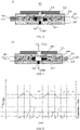
- the metal in the source electrode 201 is oxidized, and the metal cations 210 generated may directionally migrate in the first dielectric layer 202 in the horizontal direction, is generally reduced to a metal state by the electrons drifting from the programming electrode 203 during the migration process, and becomes the extension portion of the source electrode 201 in the first dielectric layer 202, thereby changing an effective area of the source electrode 201 in the horizontal direction.
- the source electrode 201, the second dielectric layer 204 and the reading electrode 207 form a capacitor 200
- the reading electrode 207 and the source electrode 201 may be regarded as upper and lower plates of the capacitor 200
- effective areas of the source electrode 201 and the reading electrode 207 may determine the effective electrode area of the capacitor 200, that is, the capacitance value of the capacitor 200.
- an effective electrode area of a capacitor is generally determined by the smaller of effective areas of upper and lower plates.
- the effective area of the reading electrode 207 may be set to be larger than the effective area of the source electrode 201, and in this case, the effective electrode area of the capacitor 200 is determined by the effective area of the source electrode 201. Therefore, the effective electrode area of the capacitor 200 may be changed by changing the effective area of the source electrode 201 in the horizontal direction, thereby changing the capacitance value of the capacitor 200.
- the effective area of the reading electrode 207 is larger than K times the effective area of the source electrode 201.
- K may be 2, 3 or the like.
- the effective area of the reading electrode 207 is larger than K times the effective area of the source electrode 201, the effective area of the source electrode 201 is not larger than an area of the reading electrode when increasing, which results in that the effective electrode area of the capacitor is limited by the effective area of the reading electrode 207.
- the effective area of the reading electrode is an area of a lower surface of the reading electrode in contact with the second dielectric layer
- the effective area of the source electrode is an area of the upper surface of the source electrode in contact with the second dielectric layer.
- different capacitance values of the capacitor 200 may be set to correspond to different storage states of the memcapacitor. It is assumed that the capacitor 200 has two states of a high capacitance value and a low capacitance value, and the two states may be set to correspond to storage states "1" and "0". For example, when the capacitance value of the capacitor 200 is a first value (corresponding to the high capacitance value), it may be set to correspond to the storage state "1", and when the capacitance value of the capacitor 200 is a second value (corresponding to the low capacitance value), it may be set to correspond to the storage state "0". Thus, by controlling the voltage difference between the source electrode 201 and the programming electrode 203, the capacitance value of the capacitor is the first value or the second value, thereby achieving writing of "0" or "1" in the memcapacitor.
- the voltage difference between the programming electrode 203 and the source electrode 201 may be controlled to be a negative value.
- the source electrode 201 is grounded, and a voltage signal less than zero is applied to the programming electrode 203.
- the metal cations 210 in the source electrode 201 migrate outward in the first dielectric layer 202, that is, in a direction of the programming electrode 203, and an effective size of the source electrode is increased or the effective area of the source electrode is increased.
- the effective electrode area of the capacitor is increased, the capacitance value of the capacitor is then increased, and the capacitance value of the capacitor at this time may be set to be the high capacitance value (or referred to as a high capacitance status), which corresponds to the storage state "1".
- the voltage difference between the programming electrode 203 and the source electrode 201 may be controlled to be a positive value.
- the source electrode 201 is grounded, and a voltage signal greater than zero is applied to the programming electrode 203.
- the metal cations 210 in the source electrode 201 migrate inward, that is, in a direction away from the programming electrode 203, and the effective size of the source electrode is reduced or the effective area of the source electrode is reduced. That is, the effective electrode area of the capacitor is reduced, the capacitance value of the capacitor is then reduced, and the capacitance value of the capacitor at this time may be set to be the low capacitance value (or referred to as a low capacitance status), which corresponds to the storage state "0".
- the capacitor 200 may further have more capacitance value status, which correspond to more storage states of the memcapacitor, and thus more storage states of the memcapacitor could be achieved by controlling the capacitor 200 to be more capacitance value status.
- the capacitor 200 may have four capacitance value status, which correspond to four storage states of the memcapacitor: "00", "01", "10” and "11". The capacitor is in the foregoing four capacitance value status by controlling the voltage difference between the source electrode 201 and the programming electrode 203, and thus the foregoing four storage states of the memcapacitor could be achieved.
- each capacitance value state of the capacitor 200 may be a specific capacitance value, or may be a specific capacitance value range. Then, the capacitance value of the capacitor 200 may be set to correspond to a certain specific storage state when being the specific capacitance value, or the capacitance value of the capacitance may be set to correspond to a certain specific storage state when falling within the specific capacitance value range, which is not limited in the embodiment of the present application.
- the source electrode 201 is grounded, and a voltage signal V1 is applied to the programming electrode 203, V1 ⁇ 0.
- V1 a voltage signal
- the metal cations 210 inside the source electrode 201 migrate outward in the horizontal direction, and the effective size of the source electrode 201 is increased from do to di, where do is the effective size of the source electrode 201 when the metal cations 210 do not migrate.
- the voltage signal V1 on the programming electrode 203 is disconnected, and the metal cations 210 stop migrating. However, due to a relaxation process, a part of the metal cations 210 may contract inward, and in this case, the effective size of the source electrode is reduced from d 1 to d 1eff .
- the capacitance value of the capacitor 200 is measured when the effective size of the source electrode 201 is d 1eff .
- an alternating current voltage signal V3 is applied to the reading electrode 207, for example, with a frequency of 1 kHz and a read voltage of 0.03V, for reading the capacitance value of the capacitor 200, which is recorded as a first capacitance value.
- the alternating current voltage signal V3 applied to the reading electrode 207 is disconnected.
- a voltage signal V2 is applied to the programming electrode 203, V2>0.
- the metal cations 210 inside the source electrode 201 migrate inward in the horizontal direction, and the effective size of the source electrode is reduced from d 1eff to d 2 .
- the voltage signal V2 on the programming electrode 203 is disconnected, and the metal cations 210 stop migrating. Similarly, due to the relaxation process, a part of the metal cations 210 may expand outward, and in this case, the size of the source electrode is increased from d 2 to d 2eff .
- the capacitance value of the capacitor 200 is measured when the effective size of the source electrode is d 2eff .
- an alternating current voltage signal V3 is applied to the reading electrode 207, for example, with a frequency of 1 kHz and a read voltage of 0.03 V, for reading the capacitance value of the capacitor 200, which is recorded as a second capacitance value.
- the alternating current voltage signal V3 applied to the reading electrode 207 is disconnected.
- the first capacitance value is greater than the second capacitance value, and it may be set that the first capacitance value is a high capacitance value and the second capacitance value is a low capacitance value, and they correspond to the storage states "1" and "0", respectively. Therefore, repeated switching of a high capacitance status or a low capacitance status of the capacitor could be achieved by controlling a voltage signal applied to the programming electrode 203, thereby achieving non-volatile storage of data "0" and "1" in the memcapacitor.
- FIG. 6 is a working timing diagram of a memcapacitor in a two-level storage scene.
- FIG. 6 is a diagram of a relationship among a capacitance value of a capacitor, a voltage signal applied to a programming electrode (that is, a program voltage) and a clock signal, where an abscissa is time, an ordinate on the left side is the program voltage, a corresponding curve of which is located at a lower position in FIG. 6 , and an ordinate on the right side is the capacitance value of the capacitor, a corresponding curve of which is located at an upper position in FIG. 6 .
- 501-504 are an erase and write cycle (or referred to as a program cycle), and 505-508 are another erase and write cycle.
- 505-508 are another erase and write cycle.
- more erase and write cycles may be included, and here only 501-504 are taken as an example for description.
- a voltage signal less than zero is applied to the programming electrode, an effective size of a source electrode is gradually increased, and the capacitance value of the capacitor is gradually increased, which correspond to the control process shown in FIG. 2 .
- the voltage signal on the programming electrode is disconnected, and the size of the source electrode shrinks slightly due to a relaxation process, and at this time, the capacitance value of the capacitor is in a high capacitance status 511, which correspond to the control process shown in FIG. 3 .
- a voltage signal greater than zero is applied to the programming electrode, the effective size of the source electrode is gradually reduced, and the capacitance value of the capacitor is gradually reduced, which correspond to the control process shown in FIG. 4 .
- the voltage signal on the programming electrode is disconnected, and the size of the source electrode expands slightly due to the relaxation process, and at this time, the capacitance value of the capacitor is in a low capacitance status 512, which correspond to the control process shown in FIG. 5 .
- the working timing of the memcapacitor shown in FIG. 6 is only an example, the embodiment of the present application may adjust the foregoing working process to implement continuous writing of "0", or continuous writing of "1” , or writing of "1" first and then writing of "0", or other timings, which will not be repeated redundantly herein.
- the memcapacitor 20 may further include: a driving module configured to control, by controlling a voltage parameter of the voltage signal applied to the programming electrode, a migration distance of the metal cations in the horizontal direction so as to control the effective electrode area of the capacitor.
- a driving module configured to control, by controlling a voltage parameter of the voltage signal applied to the programming electrode, a migration distance of the metal cations in the horizontal direction so as to control the effective electrode area of the capacitor.
- the voltage parameter includes a type of voltage and/or a corresponding control parameter
- the type of voltage is a direct current voltage or a pulse voltage
- a control parameter of the direct current voltage includes at least one of a voltage amplitude, a voltage applying time and a voltage applying manner (for example, stepping voltage applying or linear voltage applying)
- a control parameter of the pulse voltage includes at least one of a number of pulse voltages, an amplitude and a width of the pulse voltage.
- different capacitance value status of the capacitor correspond to different storage states of the memcapacitor.
- the capacitor presents different capacitance values, thereby achieving the corresponding storage states of the memcapacitor.
- FIG. 7 Four-level storage is taken as an example below to illustrate a working principle of multi-level storage of the memcapacitor with reference to FIG. 7 . It should be understood that the example shown in FIG. 7 is to make the capacitor have different capacitance values by controlling a number of pulse voltage signals applied to the programming electrode, thereby achieving the multi-level storage of the memcapacitor. Certainly, the foregoing process may be achieved by controlling other voltage parameters applied to the programming electrode, which will not be repeated redundantly herein.
- an initial capacitance value of the capacitor is at 600, which is denoted as C1.
- the capacitance value of the capacitor is increased to 601, which is denoted as C2.
- the capacitance value of the capacitor is increased to 602 or 603, respectively, which is denoted as C3 or C4, respectively.
- the capacitance value of the capacitor is reduced to zero because the voltage is excessive to cause the metal cations to move to the programming electrode such that the programming electrode and the source electrode are conducted.
- the capacitance value of the capacitor falls from 603 to 611, which is denoted as C5.
- the capacitance value of the capacitor falls to 612 or 613, which is denoted as C6 or C7, respectively.
- the foregoing capacitance values satisfy the following relationship: C4>C3 ⁇ C5>C6 ⁇ C2>C7 ⁇ C1.
- the capacitor has four capacitance values, or has four capacitance value status, and the four capacitance values may be set to correspond to four storage states, respectively.
- the correspondence may be set as follows:
- different capacitance value status of the capacitor may correspond to different storage states of the memcapacitor.
- the voltage parameter of the voltage signal applied to the programming electrode for example, the number of pulse voltages, the amplitude or the width of the pulse voltage
- the capacitor is in different capacitance value status, thereby achieving multi state storage of the memcapacitor.
- the driving module may further control the voltage parameter of the voltage signal such that a maximum migration distance of the metal cations in the first dielectric layer is less than a distance threshold to avoid conduction between the source electrode and the programming electrode due to moving of the metal cations to the programming electrode, and influence on storage of data.
- the distance threshold is 70% of a size of the first dielectric layer in the horizontal direction, that is, the metal cations move in the first dielectric layer farthest to 70% of the size of the first dielectric layer in the horizontal dimension.
- a thickness of the first dielectric layer is the same as a thickness of the source electrode to avoid moving of the metal cations in the source electrode out of the first dielectric layer in migration, and influence on control of the effective area of the source electrode.
- a thickness of the programming electrode and the thickness of the first dielectric layer may be the same, or may be different, which is not limited in the embodiment of the present application.
- mobility of the metal cations 210 in the first dielectric layer 202 is greater than mobility of the metal cations 210 in the second dielectric layer 204 and in the third dielectric layer 205.
- the first dielectric layer 202 is a transportation layer of the metal cations 210
- the second dielectric layer 204 and the third dielectric layer 205 are confinement layers of the metal cations 210.
- ratios of the mobility of the metal cations 210 in the first dielectric layer 202 to the mobility of the metal cations 210 in the second dielectric layer 204 and in the third dielectric layer 205 are greater than 10.
- a lower surface of the second dielectric layer 204 at least covers the upper surface of the source electrode 201 and the upper surface of first dielectric layer 202 so as to avoid moving of the metal cations 210 of the source electrode 201 to the reading electrode 204, conduction between the source electrode 201 and the read electrode 207, and influence on reading of data in the memcapacitor.
- an upper surface of the third dielectric layer 205 at least covers a lower surface of the source electrode 201 and a lower surface of the first dielectric layer 202.
- the thickness of the first dielectric layer 202 ranges from 10 to 100 times a radius of a metal cation 210.
- the source electrode 201 may be made of a metal material such as silver or copper.
- the metal cations may be silver ions (Ag + ), copper ions (Cu 2+ ) or the like.
- the programming electrode 203 may be made of a noble metal material having good chemical stability, such as platinum (Pt), palladium (Pd) or gold (Au).
- the reading electrode 207 may also be made of a noble metal material having good chemical stability, such as platinum (Pt), palladium (Pd) or gold (Au).
- a noble metal material having good chemical stability such as platinum (Pt), palladium (Pd) or gold (Au).
- the conductive through hole 209 may be made of metal or a semiconductor material having good electrical conductivity, such as tungsten (W), copper (Cu) or polysilicon.
- a material of the first dielectric layer 202 may be silicon dioxide (SiO 2 ) or another semiconductor material in which metal cations have less mobility.
- the second dielectric layer 204 and the third dielectric layer 205 may be made of the same material, or may be made of different materials, which is not limited in the embodiment of the present application.
- the second dielectric layer 204 and the third dielectric layer 205 may be made of one of the following materials: metal oxide materials or metal nitride materials, such as aluminum oxide (Al 2 O 3 ), zirconium oxide (ZrO 2 ), hafnium oxide (HfO 2 ), tantalum oxide (Ta 2 O 5 ) or aluminum nitride (AlN).
- metal oxide materials or metal nitride materials such as aluminum oxide (Al 2 O 3 ), zirconium oxide (ZrO 2 ), hafnium oxide (HfO 2 ), tantalum oxide (Ta 2 O 5 ) or aluminum nitride (AlN).
- the memcapacitor of the embodiment of the present application may change the capacitance value of the capacitor by changing the effective electrode area of the capacitor, and the materials of the respective structural members in the memcapacitor are common materials in the field of semiconductor industry, which could solve a problem of a complicated process due to high requirements for dielectric materials in a preparation process of an existing memcapacitor.
- FIG. 8 and FIG. 9 show two layout design schemes of the memcapacitor 20 of FIG. 1 . It should be understood that FIG 8 and FIG. 9 are cross-sectional views of the memcapacitor 20 in a horizontal direction of a source electrode.
- a source electrode 201, a first dielectric layer 202 and a programming electrode 203 in the memcapacitor may be concentric circles from inside to outside, that is, the source electrode 201 is an innermost circle, the first dielectric layer 202 is a circular ring surrounding the source electrode 201, and the programming electrode 203 is a circular ring surrounding the first dielectric layer 202.
- the source electrode 201, the first dielectric layer 202 and the programming electrode 203 may be axisymmetric in shape.
- the source electrode may be a rectangular at a middle position
- the first dielectric layer 202 is divided into two parts symmetrically distributed on two sides of the source electrode 201
- the programming electrode 203 is also divided into two parts symmetrically distributed on outer sides of the two parts of the first dielectric layer 202.
- FIG. 8 and FIG. 9 are merely possible implementation manners or preferred implementation manners of the memcapacitor structure according to an embodiment of the present application.
- Other implementation manners resulting from the memcapacitor structure according to the embodiment of the present application also fall within the protection scope of the embodiment of the present application.
- FIG. 10 is a schematic structural diagram of a memcapacitor according to another embodiment of the present application.
- the programming electrode 203 and the reading electrode 207 are combined into a same electrode, and in this way, a number of ports of the memcapacitor is reduced from three to two and the structure is simpler, which benefit improvement of integration of a device.
- external ports of the memcapacitor include three ports of the source electrode, the programming electrode and the reading electrode.
- external ports of the memcapacitor include two ports of the source electrode and the combined electrode of the programming electrode and the reading electrode.
- a program voltage when a program voltage is much greater than a read voltage (for example, a ratio of the program voltage to the read voltage is greater than or equal to 10), the read voltage applied may not significantly affect an effective area of the source electrode in reading data, and thus the reading electrode and the programming electrode may be combined into a same electrode.
- FIG. 11 is a schematic flow chart of a programming method 70 for a memcapacitor according to an embodiment of the present application.
- the programming method 70 may be applied to a memcapacitor, the memcapacitor includes:
- the memcapacitor may be the memcapacitor 20 of the embodiments of the present application.
- reference may be made to the related descriptions of the foregoing embodiments, which will not be repeated redundantly herein.
- S71 specifically includes: controlling, by controlling a voltage parameter of a voltage signal applied to the programming electrode, a migration distance of metal cations in the source electrode in the horizontal direction so as to control the effective electrode area of the capacitor, where different capacitance values of the capacitor correspond to different storage states of the memcapacitor.
- the voltage parameter includes a type of voltage and/or a corresponding control parameter
- the type of voltage is a direct current voltage or a pulse voltage
- a control parameter of the direct current voltage includes at least one of a voltage amplitude, a voltage applying time and a voltage applying manner
- a control parameter of the pulse voltage includes at least one of a number of pulse voltages, an amplitude and a width of the pulse voltage.
- controlling, by controlling the voltage parameter of the voltage signal applied to the programming electrode, the migration distance of the metal cations in the source electrode in the horizontal direction includes:
- controlling, by controlling the voltage parameter of the voltage signal applied to the programming electrode, the migration distance of the metal cations in the source electrode in the horizontal direction includes: controlling, by controlling the voltage parameter of the voltage signal input to the programming electrode, a maximum migration distance of the metal cations in the first dielectric layer to be not more than 70% of a size of the first dielectric layer in the horizontal direction.
- the memcapacitor further includes:
- mobility of metal cations in the source electrode in the first dielectric layer is greater than mobility of the metal cations in the second dielectric layer, and the mobility of the metal cations in the first dielectric layer is greater than mobility of the metal cations in the third dielectric layer.
- a ratio of the mobility of the metal cations in the first dielectric layer to the mobility of the metal cations in the second dielectric layer is greater than or equal to 10
- a ratio of the mobility of the metal cations in the first dielectric layer to the mobility of the metal cations in the third dielectric layer is greater than or equal to 10.
- the reading electrode is connected with the programming electrode.
- the reading electrode and the programming electrode are connected as one electrode in a case that a ratio of a program voltage to a read voltage is greater than or equal to 10.
- the first dielectric layer surrounds the source electrode, and the programming electrode surrounds the first dielectric layer.
- a thickness of the first dielectric layer is the same as a thickness of the source electrode, and a thickness of the programming electrode is the same as the thickness of the source electrode.
- An embodiment of the present application further provides a capacitive random access memory CRAM, as shown in FIG. 12 .
- a capacitive random access memory 80 includes a memcapacitor array 81, the memcapacitor array 81 may be an array composed of several memcapacitors 20 according to the embodiment of the present application, and each memcapacitor unit in the memcapacitor array 81 may perform storage of data using the programming method 70 shown in FIG. 11 .
- An embodiment not being part of the present application further provides a computer readable storage medium, where the computer readable storage medium stores one or more programs, and the one or more programs include an instruction.
- the instruction is executed by a portable electronic device that includes a plurality of application programs, the portable electronic device can execute the method of the embodiment shown in FIG. 11 .
- An embodiment not being part of the present application further provides a computer program including instructions that, when executed by a computer, cause the computer to execute the method of the embodiment shown in FIG. 11 .
- An embodiment not being part of the present application further provides a chip including an input and output interface, at least one processor, at least one memory and a bus, where the at least one memory is configured to store an instruction, the at least one processor is configured to call an instruction in the at least one memory to execute the method of the embodiment shown in FIG. 11 .
- the disclosed system, apparatus, and method may be implemented in another manner.
- the described apparatus embodiment is merely an example.
- the unit division is merely logical function division and may be other division in actual implementation.
- a plurality of units or components may be combined or integrated into another system, or some features may be ignored or not performed.
- the displayed or discussed mutual couplings or direct couplings or communication connections may be implemented by using some interfaces.
- the indirect couplings or communication connections between the apparatuses or units may be implemented in electrical, mechanical, or other forms.
- the units described as separate components may or may not be physically separate, and components displayed as units may or may not be physical units, may be located in one position, or may be distributed on multiple network units. Some or all of the units may be selected according to actual requirements to achieve the objectives of the solutions of the embodiments.
- functional units in the embodiments of the present application may be integrated into one processing unit, or each of the units may exist alone physically, or two or more units are integrated into one unit.
- the functions When the functions are implemented in the form of a software functional unit and sold or used as an independent product, the functions may be stored in a computer-readable storage medium.
- the computer software product is stored in a storage medium and includes several instructions for instructing a computer device (which may be a personal computer, a server, a network device, or the like) to perform all or some of the steps of the methods described in the embodiments of the present application.
- the foregoing storage medium includes: any medium that can store program code, such as a USB flash drive, a removable hard disk, a read-only memory (ROM), a random access memory (RAM), a magnetic disk, or an optical disc.
Landscapes
- Engineering & Computer Science (AREA)
- Computer Hardware Design (AREA)
- Power Engineering (AREA)
- Semiconductor Memories (AREA)
Claims (14)
- Speicherkondensator, umfassend:eine Source-Elektrode (201), die aus einem Metallmaterial hergestellt ist;eine erste dielektrische Schicht (202), die in einer horizontalen Richtung an Außenseiten der Source-Elektrode (201) angeordnet ist, wobei die erste dielektrische Schicht (202) in Kontakt mit der Source-Elektrode (201) steht;eine Programmierelektrode (203), die in der horizontalen Richtung an Außenseiten der ersten dielektrischen Schicht (202) angeordnet ist, wobei die Außenseiten der ersten dielektrischen Schicht (202) nicht in Kontakt mit der Source-Elektrode (201) stehen, wobei die Programmierelektrode (203) in Kontakt mit der ersten dielektrischen Schicht (202) steht;eine zweite dielektrische Schicht (204), die an einer oberen Fläche der Source-Elektrode (201) und einer oberen Fläche der ersten dielektrischen Schicht (202) angeordnet ist, wobei die zweite dielektrische Schicht (204) in Kontakt mit der Source-Elektrode (201) und der ersten dielektrischen Schicht (202) steht;eine Ausleseelektrode (207), die an einer oberen Fläche der zweiten dielektrischen Schicht (204) angeordnet ist, wobei die Ausleseelektrode (207), die zweite dielektrische Schicht (204) und die Source-Elektrode (201) einen Kondensator (200) bilden, wobei die Ausleseelektrode (207) in Kontakt mit der zweiten dielektrischen Schicht (204) steht;eine dritte dielektrische Schicht (205), die an einer unteren Fläche der Source-Elektrode (201) und einer unteren Fläche der ersten dielektrischen Schicht (202) angeordnet ist, wobei die dritte dielektrische Schicht (205) in Kontakt mit der Source-Elektrode (201) und der ersten dielektrischen Schicht (202) steht; und eine leitende Durchgangsbohrung (209), die in der dritten dielektrischen Schicht (205) angeordnet ist und sich zum Anschließen der Source-Elektrode (201) an eine Fremdspannung unter der Source-Elektrode (201) befindet.
- Speicherkondensator nach Anspruch 1, wobei die dritte dielektrische Schicht (205) zumindest die untere Fläche der Source-Elektrode (201) und die untere Fläche der ersten dielektrischen Schicht (202) bedeckt; und/oder
eine Beweglichkeit von Metallkationen in der ersten dielektrischen Schicht (202) höher als eine Beweglichkeit der Metallkationen in der zweiten dielektrischen Schicht (204) ist, und die Beweglichkeit der Metallkationen in der ersten dielektrischen Schicht (202) höher als eine Beweglichkeit der Metallkationen in der dritten dielektrischen Schicht (205) ist, wobei die Metallkationen von der Source-Elektrode (201) erzeugt werden. - Speicherkondensator nach Anspruch 2, wobei eine Verhältniszahl von der Beweglichkeit der Metallkationen in der ersten dielektrischen Schicht (202) zu der Beweglichkeit der Metallkationen in der zweiten dielektrischen Schicht (204) größer als oder gleich 10 ist, und eine Verhältniszahl von der Beweglichkeit der Metallkationen in der ersten dielektrischen Schicht (202) zu der Beweglichkeit der Metallkationen in der dritten dielektrischen Schicht (205) größer als oder gleich 10 ist.
- Speicherkondensator nach einem beliebigen der Ansprüche 1 bis 3, wobei die zweite dielektrische Schicht (204) zumindest die obere Fläche der Source-Elektrode (201) und die obere Fläche der ersten dielektrischen Schicht (202) bedeckt; und/oder
ein Bereich einer unteren Fläche der Ausleseelektrode (207) in einem Fall, dass keine Spannungsdifferenz zwischen der Source-Elektrode (201) und der Programmierelektrode (203) vorliegt, größer als das Zweifache eines Bereichs der oberen Fläche der Source-Elektrode (201) ist. - Speicherkondensator nach einem beliebigen der Ansprüche 1 bis 4, wobei eine Dicke der ersten dielektrischen Schicht (202) in einem Bereich des 10- bis 100-Fachen eines Radius eines Metallkations in der Source-Elektrode (201) liegt.
- Speicherkondensator nach einem beliebigen der Ansprüche 1 bis 5, wobei der Speicherkondensator ferner Folgendes umfasst:
ein Ansteuermodul, das so ausgestaltet ist, dass es, durch Anlegen eines Spannungsparameters an die Programmierelektrode (203), Metallkationen in der Source-Elektrode (201) so steuert, dass sie in der horizontalen Richtung wandern, so dass ein wirksamer Elektrodenbereich des Kondensators (200) verändert wird, wobei unterschiedliche Kapazitätswerte des Kondensators (200) unterschiedlichen Speicherzuständen des Speicherkondensators entsprechen. - Speicherkondensator nach Anspruch 6, wobei das Ansteuermodul ausgestaltet ist zum:
Steuern, durch Steuern eines an die Programmierelektrode (203) angelegten Spannungsparameters, einer Wanderungsdistanz der Metallkationen in der horizontalen Richtung, so dass der wirksame Elektrodenbereich des Kondensators (200) gesteuert wird. - Speicherkondensator nach Anspruch 7, wobei der Spannungsparameter einen Spannungstyp und/oder einen entsprechenden Steuerparameter umfasst, der Spannungstyp eine Gleichstromspannung oder eine Impulsspannung ist, ein Steuerparameter der Gleichstromspannung mindestens eines von einer Spannungsamplitude, einer Spannungsanlegezeit und einer Spannungsanlegeart umfasst, und ein Steuerparameter der Impulsspannung mindestens eines von einer Reihe von Impuls spannungen, einer Amplitude und einer Breite der Impulsspannung umfasst.
- Speicherkondensator nach einem beliebigen der Ansprüche 6 bis 8, wobei das Ansteuermodul ausgestaltet ist zum:Eingeben eines ersten Spannungsparameters in die Programmierelektrode (203) während eines ersten Zeitraums, wobei ein Spannungswert des ersten Spannungsparameters kleiner als Null ist, die Source-Elektrode (201) geerdet ist, die Metallkationen in der Source-Elektrode (201) in der horizontalen Richtung nach außen wandern, und eine Größe der Source-Elektrode (201) in der horizontalen Richtung von einer ersten Größe auf eine zweite Größe vergrößert wird,Unterbrechen des ersten Spannungsparameters während eines zweiten Zeitraums, wobei die Metallkationen in der Source-Elektrode (201) aufhören zu wandern, und die Größe der Source-Elektrode (201) in der horizontalen Richtung von der zweiten Größe auf eine zweite wirksame Größe verringert wird, wobei ein Kapazitätswert des Kondensators (200) einem ersten Speicherzustand von mindestens zwei Speicherzuständen des Speicherkondensators entspricht, wenn die Größe der Source-Elektrode (201) in der horizontalen Richtung die zweite wirksame Größe ist; oderEingeben eines zweiten Spannungsparameters in die Programmierelektrode (203) während eines dritten Zeitraums, wobei ein Spannungswert des zweiten Spannungsparameters größer als Null ist, die Source-Elektrode (201) geerdet ist, die Metallkationen in der Source-Elektrode (201) in der horizontalen Richtung nach innen wandern, und die Größe der Source-Elektrode (201) in der horizontalen Richtung von einer dritten Größe auf eine vierte Größe verringert wird,Unterbrechen des zweiten Spannungsparameters während eines vierten Zeitraums, wobei die Metallkationen in der Source-Elektrode (201) aufhören zu wandern, und die Größe der Source-Elektrode (201) in der horizontalen Richtung von der vierten Größe auf eine vierte wirksame Größe vergrößert wird, wobei der Kapazitätswert des Kondensators (200) einem zweiten Speicherzustand der mindestens zwei Speicherzustände des Speicherkondensators entspricht, wenn die Größe der Source-Elektrode (201) in der horizontalen Richtung die vierte wirksame Größe ist.
- Speicherkondensator nach Anspruch 1, wobei die Ausleseelektrode (207) und die Programmierelektrode (203) in einem Fall, dass eine Verhältniszahl von einer Programmierspannung zu einer Auslesespannung größer als oder gleich 10 ist, als eine Elektrode angeschlossen sind.
- Speicherkondensator nach einem beliebigen der Ansprüche 1 bis 10, wobei die erste dielektrische Schicht (202) die Source-Elektrode (201) umgibt, und die Programmierelektrode (203) die erste dielektrische Schicht (202) umgibt.
- Speicherkondensator nach einem beliebigen der Ansprüche 1 bis 11, wobei eine Dicke der ersten dielektrischen Schicht (202) die gleiche wie eine Dicke der Source-Elektrode (201) ist, und eine Dicke der Programmierelektrode (203) die gleiche wie die Dicke der Source-Elektrode (201) ist.
- Programmierverfahren für einen Speicherkondensator nach einem beliebigen der Ansprüche 1-12, umfassend:
Anlegen (71) einer Spannungsdifferenz zwischen der Source-Elektrode und der Programmierelektrode, um einen wirksamen Elektrodenbereich des Kondensators zu verändern. - Kapazitiver Speicher, umfassend:
ein Speicherkondensatorarray, wobei das Speicherkondensatorarray ein Array ist, das aus einer Vielzahl von Speicherkondensatoren nach einem beliebigen der Ansprüche 1 bis 12 zusammengesetzt ist.
Applications Claiming Priority (1)
| Application Number | Priority Date | Filing Date | Title |
|---|---|---|---|
| PCT/CN2018/113978 WO2020093199A1 (zh) | 2018-11-05 | 2018-11-05 | 忆容器、忆容器的编程方法和容变式存储器 |
Publications (3)
| Publication Number | Publication Date |
|---|---|
| EP3680906A1 EP3680906A1 (de) | 2020-07-15 |
| EP3680906A4 EP3680906A4 (de) | 2020-09-02 |
| EP3680906B1 true EP3680906B1 (de) | 2022-08-31 |
Family
ID=70458912
Family Applications (1)
| Application Number | Title | Priority Date | Filing Date |
|---|---|---|---|
| EP18918410.4A Active EP3680906B1 (de) | 2018-11-05 | 2018-11-05 | Speicherkondensator und programmierverfahren dafür und kapazitiver speicher |
Country Status (4)
| Country | Link |
|---|---|
| US (1) | US10885965B2 (de) |
| EP (1) | EP3680906B1 (de) |
| CN (1) | CN111480201B (de) |
| WO (1) | WO2020093199A1 (de) |
Family Cites Families (23)
| Publication number | Priority date | Publication date | Assignee | Title |
|---|---|---|---|---|
| US5761115A (en) | 1996-05-30 | 1998-06-02 | Axon Technologies Corporation | Programmable metallization cell structure and method of making same |
| US6984555B2 (en) * | 2003-11-03 | 2006-01-10 | Infineon Technologies Ag | Device and method for inhibiting oxidation of contact plugs in ferroelectric capacitor devices |
| US20080273370A1 (en) * | 2007-05-02 | 2008-11-06 | Jan Keller | Integrated Circuit, Method of Operating an Integrated Circuit, Memory Cell Array, and Memory Module |
| WO2010144092A1 (en) * | 2009-06-12 | 2010-12-16 | Hewlett-Packard Development Company, L.P. | Capacitive crossbar arrays |
| US8750024B2 (en) * | 2009-06-18 | 2014-06-10 | Hewlett-Packard Development Company, L.P. | Memcapacitor |
| US8779848B2 (en) * | 2009-08-28 | 2014-07-15 | Hewlett-Packard Development Company, L.P. | Two terminal memcapacitor device |
| US8437174B2 (en) | 2010-02-15 | 2013-05-07 | Micron Technology, Inc. | Memcapacitor devices, field effect transistor devices, non-volatile memory arrays, and methods of programming |
| US8416609B2 (en) * | 2010-02-15 | 2013-04-09 | Micron Technology, Inc. | Cross-point memory cells, non-volatile memory arrays, methods of reading a memory cell, methods of programming a memory cell, methods of writing to and reading from a memory cell, and computer systems |
| JP2013114731A (ja) * | 2011-11-30 | 2013-06-10 | Toshiba Corp | 半導体記憶装置 |
| US8767438B2 (en) * | 2012-03-19 | 2014-07-01 | Hewlett-Packard Development Company, L.P. | Memelectronic device |
| EP2842165A4 (de) * | 2012-04-26 | 2015-10-14 | Hewlett Packard Development Co | Nichtlineare anpassbare elektrische vorrichtungen |
| US8799848B1 (en) * | 2013-01-15 | 2014-08-05 | International Business Machines Corporation | Methods for modeling of FinFET width quantization |
| US8835272B1 (en) * | 2013-02-28 | 2014-09-16 | Sandia Corporation | Passive electrically switchable circuit element having improved tunability and method for its manufacture |
| WO2015167351A1 (en) * | 2014-04-30 | 2015-11-05 | Nokia Technologies Oy | Memristor and method of production thereof |
| WO2016068886A1 (en) * | 2014-10-28 | 2016-05-06 | Hewlett Packard Enterprise Development Lp | Memcapacitive cross-bar array for determining a dot product |
| US9990580B2 (en) * | 2015-03-13 | 2018-06-05 | International Business Machines Corporation | Neuromorphic synapses |
| US10162263B2 (en) * | 2015-04-27 | 2018-12-25 | Hewlett-Packard Development Company, L.P. | Dynamic logic memcap |
| CN105679840B (zh) | 2016-04-11 | 2018-07-13 | 南京大学 | 一种新型贴片式忆容器及其制备方法 |
| JP6602279B2 (ja) * | 2016-09-20 | 2019-11-06 | 株式会社東芝 | メムキャパシタ、ニューロ素子およびニューラルネットワーク装置 |
| JP7031891B2 (ja) * | 2016-12-02 | 2022-03-08 | カーバー サイエンティフィック インコーポレイテッド | メモリデバイス及び容量性エネルギー蓄積デバイス |
| US10636552B2 (en) * | 2017-03-20 | 2020-04-28 | Gwangju Institute Of Science And Technology | Multi-function electronic device having memristor and memcapacitor and method for manufacturing the same |
| KR102013858B1 (ko) * | 2017-03-20 | 2019-08-23 | 광주과학기술원 | 멤리스터 및 멤커패시터 다기능 전자소자 및 그 제조방법 |
| KR20180115995A (ko) * | 2017-04-14 | 2018-10-24 | 명지대학교 산학협력단 | 멤캐패시터를 이용한 트랜지스터 소자 및 그 제조방법 |
-
2018
- 2018-11-05 EP EP18918410.4A patent/EP3680906B1/de active Active
- 2018-11-05 WO PCT/CN2018/113978 patent/WO2020093199A1/zh not_active Ceased
- 2018-11-05 CN CN201880002043.XA patent/CN111480201B/zh active Active
-
2019
- 2019-11-19 US US16/687,694 patent/US10885965B2/en active Active
Also Published As
| Publication number | Publication date |
|---|---|
| WO2020093199A1 (zh) | 2020-05-14 |
| EP3680906A4 (de) | 2020-09-02 |
| EP3680906A1 (de) | 2020-07-15 |
| CN111480201A (zh) | 2020-07-31 |
| US10885965B2 (en) | 2021-01-05 |
| US20200143864A1 (en) | 2020-05-07 |
| CN111480201B (zh) | 2023-10-17 |
Similar Documents
| Publication | Publication Date | Title |
|---|---|---|
| EP2386115B1 (de) | Speicherzelle mit dielektrischem speicherelement | |
| CN102754207B (zh) | 电阻式存储器及处理电阻式存储器的方法 | |
| CN1953230B (zh) | 包括纳米点的非易失性存储器件及其制造方法 | |
| CN104303286B (zh) | 具有局限细丝形成的电阻性存储器 | |
| KR102011551B1 (ko) | 가변 스위칭 특징들을 갖는 저항성 랜덤 액세스 메모리 셀들 | |
| JP2017521854A (ja) | 酸化物系三端子抵抗スイッチングロジックデバイス | |
| US20180075904A1 (en) | Memristive crossbar array having multi-selector memristor cells | |
| US11211555B2 (en) | Memory device and a method for forming the memory device | |
| CN108886094A (zh) | 用于形成电阻式随机存取存储器(rram)单元细丝的多阶电压 | |
| CN117135932A (zh) | 电阻存储器装置及其制造方法 | |
| KR102535415B1 (ko) | 저항 변화 메모리 장치 | |
| US8503255B2 (en) | Semiconductor storage device including plural clock oscillator circuits operating at different frequencies | |
| KR102249655B1 (ko) | 뉴런 및 이를 포함하는 뉴로모픽 시스템 | |
| EP3238252A1 (de) | Ndr-vorrichtung auf der basis von schnellen diffusiven metallatomen | |
| US10885965B2 (en) | Memcapacitor, programming method for memcapacitor and capacitive random access memory | |
| US20140374693A1 (en) | Varied multilayer memristive device | |
| JP7730248B2 (ja) | 調整可能な抵抗素子を備えるデバイス | |
| US20160155619A1 (en) | Forming memory using high power impulse magnetron sputtering | |
| CN116601709A (zh) | 使用互补开关的存储器内电阻式随机存取存储器xor逻辑 | |
| US20170133588A1 (en) | Resistive ram cell with focused electric field | |
| TWI626654B (zh) | 電阻式記憶體及其電阻式記憶胞的恢復電阻窗口方法 | |
| CN117378294A (zh) | 具有中间电极的reram模块 | |
| US20200343303A1 (en) | Reducing rram relaxation in crossbar arrays for low current applications | |
| US11568927B2 (en) | Two-terminal non-volatile memory cell for decoupled read and write operations | |
| KR102866049B1 (ko) | 비-이진 로직들을 위한 강유전체 나노입자 커패시터 및 동작 방법 |
Legal Events
| Date | Code | Title | Description |
|---|---|---|---|
| STAA | Information on the status of an ep patent application or granted ep patent |
Free format text: STATUS: UNKNOWN |
|
| STAA | Information on the status of an ep patent application or granted ep patent |
Free format text: STATUS: THE INTERNATIONAL PUBLICATION HAS BEEN MADE |
|
| PUAI | Public reference made under article 153(3) epc to a published international application that has entered the european phase |
Free format text: ORIGINAL CODE: 0009012 |
|
| STAA | Information on the status of an ep patent application or granted ep patent |
Free format text: STATUS: REQUEST FOR EXAMINATION WAS MADE |
|
| 17P | Request for examination filed |
Effective date: 20191120 |
|
| AK | Designated contracting states |
Kind code of ref document: A1 Designated state(s): AL AT BE BG CH CY CZ DE DK EE ES FI FR GB GR HR HU IE IS IT LI LT LU LV MC MK MT NL NO PL PT RO RS SE SI SK SM TR |
|
| AX | Request for extension of the european patent |
Extension state: BA ME |
|
| RIN1 | Information on inventor provided before grant (corrected) |
Inventor name: SHEN, JIAN Inventor name: YAO, GUOFENG |
|
| A4 | Supplementary search report drawn up and despatched |
Effective date: 20200730 |
|
| RIC1 | Information provided on ipc code assigned before grant |
Ipc: H01L 27/115 20170101ALI20200724BHEP Ipc: G11C 11/56 20060101ALI20200724BHEP Ipc: G11C 11/24 20060101AFI20200724BHEP Ipc: H01L 45/00 20060101ALI20200724BHEP |
|
| STAA | Information on the status of an ep patent application or granted ep patent |
Free format text: STATUS: EXAMINATION IS IN PROGRESS |
|
| 17Q | First examination report despatched |
Effective date: 20210518 |
|
| DAV | Request for validation of the european patent (deleted) | ||
| DAX | Request for extension of the european patent (deleted) | ||
| REG | Reference to a national code |
Ref country code: DE Ref legal event code: R079 Ref document number: 602018040196 Country of ref document: DE Free format text: PREVIOUS MAIN CLASS: G11C0011240000 Ipc: G11C0013000000 |
|
| RIC1 | Information provided on ipc code assigned before grant |
Ipc: H01L 49/02 20060101ALI20220518BHEP Ipc: H01L 45/00 20060101ALI20220518BHEP Ipc: G11C 11/56 20060101ALI20220518BHEP Ipc: G11C 13/00 20060101AFI20220518BHEP |
|
| GRAP | Despatch of communication of intention to grant a patent |
Free format text: ORIGINAL CODE: EPIDOSNIGR1 |
|
| STAA | Information on the status of an ep patent application or granted ep patent |
Free format text: STATUS: GRANT OF PATENT IS INTENDED |
|
| GRAS | Grant fee paid |
Free format text: ORIGINAL CODE: EPIDOSNIGR3 |
|
| GRAA | (expected) grant |
Free format text: ORIGINAL CODE: 0009210 |
|
| STAA | Information on the status of an ep patent application or granted ep patent |
Free format text: STATUS: THE PATENT HAS BEEN GRANTED |
|
| INTG | Intention to grant announced |
Effective date: 20220713 |
|
| AK | Designated contracting states |
Kind code of ref document: B1 Designated state(s): AL AT BE BG CH CY CZ DE DK EE ES FI FR GB GR HR HU IE IS IT LI LT LU LV MC MK MT NL NO PL PT RO RS SE SI SK SM TR |
|
| REG | Reference to a national code |
Ref country code: CH Ref legal event code: EP Ref country code: GB Ref legal event code: FG4D |
|
| REG | Reference to a national code |
Ref country code: AT Ref legal event code: REF Ref document number: 1515895 Country of ref document: AT Kind code of ref document: T Effective date: 20220915 |
|
| REG | Reference to a national code |
Ref country code: DE Ref legal event code: R096 Ref document number: 602018040196 Country of ref document: DE |
|
| REG | Reference to a national code |
Ref country code: IE Ref legal event code: FG4D |
|
| REG | Reference to a national code |
Ref country code: LT Ref legal event code: MG9D |
|
| REG | Reference to a national code |
Ref country code: NL Ref legal event code: MP Effective date: 20220831 |
|
| PG25 | Lapsed in a contracting state [announced via postgrant information from national office to epo] |
Ref country code: SE Free format text: LAPSE BECAUSE OF FAILURE TO SUBMIT A TRANSLATION OF THE DESCRIPTION OR TO PAY THE FEE WITHIN THE PRESCRIBED TIME-LIMIT Effective date: 20220831 Ref country code: RS Free format text: LAPSE BECAUSE OF FAILURE TO SUBMIT A TRANSLATION OF THE DESCRIPTION OR TO PAY THE FEE WITHIN THE PRESCRIBED TIME-LIMIT Effective date: 20220831 Ref country code: NO Free format text: LAPSE BECAUSE OF FAILURE TO SUBMIT A TRANSLATION OF THE DESCRIPTION OR TO PAY THE FEE WITHIN THE PRESCRIBED TIME-LIMIT Effective date: 20221130 Ref country code: LV Free format text: LAPSE BECAUSE OF FAILURE TO SUBMIT A TRANSLATION OF THE DESCRIPTION OR TO PAY THE FEE WITHIN THE PRESCRIBED TIME-LIMIT Effective date: 20220831 Ref country code: LT Free format text: LAPSE BECAUSE OF FAILURE TO SUBMIT A TRANSLATION OF THE DESCRIPTION OR TO PAY THE FEE WITHIN THE PRESCRIBED TIME-LIMIT Effective date: 20220831 Ref country code: FI Free format text: LAPSE BECAUSE OF FAILURE TO SUBMIT A TRANSLATION OF THE DESCRIPTION OR TO PAY THE FEE WITHIN THE PRESCRIBED TIME-LIMIT Effective date: 20220831 |
|
| REG | Reference to a national code |
Ref country code: AT Ref legal event code: MK05 Ref document number: 1515895 Country of ref document: AT Kind code of ref document: T Effective date: 20220831 |
|
| PG25 | Lapsed in a contracting state [announced via postgrant information from national office to epo] |
Ref country code: PL Free format text: LAPSE BECAUSE OF FAILURE TO SUBMIT A TRANSLATION OF THE DESCRIPTION OR TO PAY THE FEE WITHIN THE PRESCRIBED TIME-LIMIT Effective date: 20220831 Ref country code: IS Free format text: LAPSE BECAUSE OF FAILURE TO SUBMIT A TRANSLATION OF THE DESCRIPTION OR TO PAY THE FEE WITHIN THE PRESCRIBED TIME-LIMIT Effective date: 20221231 Ref country code: HR Free format text: LAPSE BECAUSE OF FAILURE TO SUBMIT A TRANSLATION OF THE DESCRIPTION OR TO PAY THE FEE WITHIN THE PRESCRIBED TIME-LIMIT Effective date: 20220831 Ref country code: GR Free format text: LAPSE BECAUSE OF FAILURE TO SUBMIT A TRANSLATION OF THE DESCRIPTION OR TO PAY THE FEE WITHIN THE PRESCRIBED TIME-LIMIT Effective date: 20221201 |
|
| PG25 | Lapsed in a contracting state [announced via postgrant information from national office to epo] |
Ref country code: ES Free format text: LAPSE BECAUSE OF FAILURE TO SUBMIT A TRANSLATION OF THE DESCRIPTION OR TO PAY THE FEE WITHIN THE PRESCRIBED TIME-LIMIT Effective date: 20220831 Ref country code: DK Free format text: LAPSE BECAUSE OF FAILURE TO SUBMIT A TRANSLATION OF THE DESCRIPTION OR TO PAY THE FEE WITHIN THE PRESCRIBED TIME-LIMIT Effective date: 20220831 Ref country code: CZ Free format text: LAPSE BECAUSE OF FAILURE TO SUBMIT A TRANSLATION OF THE DESCRIPTION OR TO PAY THE FEE WITHIN THE PRESCRIBED TIME-LIMIT Effective date: 20220831 Ref country code: AT Free format text: LAPSE BECAUSE OF FAILURE TO SUBMIT A TRANSLATION OF THE DESCRIPTION OR TO PAY THE FEE WITHIN THE PRESCRIBED TIME-LIMIT Effective date: 20220831 Ref country code: SM Free format text: LAPSE BECAUSE OF FAILURE TO SUBMIT A TRANSLATION OF THE DESCRIPTION OR TO PAY THE FEE WITHIN THE PRESCRIBED TIME-LIMIT Effective date: 20220831 Ref country code: RO Free format text: LAPSE BECAUSE OF FAILURE TO SUBMIT A TRANSLATION OF THE DESCRIPTION OR TO PAY THE FEE WITHIN THE PRESCRIBED TIME-LIMIT Effective date: 20220831 Ref country code: PT Free format text: LAPSE BECAUSE OF FAILURE TO SUBMIT A TRANSLATION OF THE DESCRIPTION OR TO PAY THE FEE WITHIN THE PRESCRIBED TIME-LIMIT Effective date: 20230102 |
|
| PG25 | Lapsed in a contracting state [announced via postgrant information from national office to epo] |
Ref country code: SK Free format text: LAPSE BECAUSE OF FAILURE TO SUBMIT A TRANSLATION OF THE DESCRIPTION OR TO PAY THE FEE WITHIN THE PRESCRIBED TIME-LIMIT Effective date: 20220831 Ref country code: EE Free format text: LAPSE BECAUSE OF FAILURE TO SUBMIT A TRANSLATION OF THE DESCRIPTION OR TO PAY THE FEE WITHIN THE PRESCRIBED TIME-LIMIT Effective date: 20220831 |
|
| REG | Reference to a national code |
Ref country code: DE Ref legal event code: R097 Ref document number: 602018040196 Country of ref document: DE |
|
| PG25 | Lapsed in a contracting state [announced via postgrant information from national office to epo] |
Ref country code: NL Free format text: LAPSE BECAUSE OF FAILURE TO SUBMIT A TRANSLATION OF THE DESCRIPTION OR TO PAY THE FEE WITHIN THE PRESCRIBED TIME-LIMIT Effective date: 20220831 Ref country code: MC Free format text: LAPSE BECAUSE OF FAILURE TO SUBMIT A TRANSLATION OF THE DESCRIPTION OR TO PAY THE FEE WITHIN THE PRESCRIBED TIME-LIMIT Effective date: 20220831 Ref country code: AL Free format text: LAPSE BECAUSE OF FAILURE TO SUBMIT A TRANSLATION OF THE DESCRIPTION OR TO PAY THE FEE WITHIN THE PRESCRIBED TIME-LIMIT Effective date: 20220831 |
|
| REG | Reference to a national code |
Ref country code: CH Ref legal event code: PL |
|
| PLBE | No opposition filed within time limit |
Free format text: ORIGINAL CODE: 0009261 |
|
| STAA | Information on the status of an ep patent application or granted ep patent |
Free format text: STATUS: NO OPPOSITION FILED WITHIN TIME LIMIT |
|
| GBPC | Gb: european patent ceased through non-payment of renewal fee |
Effective date: 20221130 |
|
| REG | Reference to a national code |
Ref country code: BE Ref legal event code: MM Effective date: 20221130 |
|
| PG25 | Lapsed in a contracting state [announced via postgrant information from national office to epo] |
Ref country code: LI Free format text: LAPSE BECAUSE OF NON-PAYMENT OF DUE FEES Effective date: 20221130 Ref country code: CH Free format text: LAPSE BECAUSE OF NON-PAYMENT OF DUE FEES Effective date: 20221130 |
|
| 26N | No opposition filed |
Effective date: 20230601 |
|
| PG25 | Lapsed in a contracting state [announced via postgrant information from national office to epo] |
Ref country code: SI Free format text: LAPSE BECAUSE OF FAILURE TO SUBMIT A TRANSLATION OF THE DESCRIPTION OR TO PAY THE FEE WITHIN THE PRESCRIBED TIME-LIMIT Effective date: 20220831 Ref country code: LU Free format text: LAPSE BECAUSE OF NON-PAYMENT OF DUE FEES Effective date: 20221105 |
|
| PG25 | Lapsed in a contracting state [announced via postgrant information from national office to epo] |
Ref country code: IE Free format text: LAPSE BECAUSE OF NON-PAYMENT OF DUE FEES Effective date: 20221105 Ref country code: GB Free format text: LAPSE BECAUSE OF NON-PAYMENT OF DUE FEES Effective date: 20221130 |
|
| PG25 | Lapsed in a contracting state [announced via postgrant information from national office to epo] |
Ref country code: FR Free format text: LAPSE BECAUSE OF NON-PAYMENT OF DUE FEES Effective date: 20221130 Ref country code: BE Free format text: LAPSE BECAUSE OF NON-PAYMENT OF DUE FEES Effective date: 20221130 |
|
| PG25 | Lapsed in a contracting state [announced via postgrant information from national office to epo] |
Ref country code: HU Free format text: LAPSE BECAUSE OF FAILURE TO SUBMIT A TRANSLATION OF THE DESCRIPTION OR TO PAY THE FEE WITHIN THE PRESCRIBED TIME-LIMIT; INVALID AB INITIO Effective date: 20181105 |
|
| PG25 | Lapsed in a contracting state [announced via postgrant information from national office to epo] |
Ref country code: CY Free format text: LAPSE BECAUSE OF FAILURE TO SUBMIT A TRANSLATION OF THE DESCRIPTION OR TO PAY THE FEE WITHIN THE PRESCRIBED TIME-LIMIT Effective date: 20220831 |
|
| PG25 | Lapsed in a contracting state [announced via postgrant information from national office to epo] |
Ref country code: MK Free format text: LAPSE BECAUSE OF FAILURE TO SUBMIT A TRANSLATION OF THE DESCRIPTION OR TO PAY THE FEE WITHIN THE PRESCRIBED TIME-LIMIT Effective date: 20220831 Ref country code: IT Free format text: LAPSE BECAUSE OF FAILURE TO SUBMIT A TRANSLATION OF THE DESCRIPTION OR TO PAY THE FEE WITHIN THE PRESCRIBED TIME-LIMIT Effective date: 20220831 |
|
| PG25 | Lapsed in a contracting state [announced via postgrant information from national office to epo] |
Ref country code: TR Free format text: LAPSE BECAUSE OF FAILURE TO SUBMIT A TRANSLATION OF THE DESCRIPTION OR TO PAY THE FEE WITHIN THE PRESCRIBED TIME-LIMIT Effective date: 20220831 |
|
| PG25 | Lapsed in a contracting state [announced via postgrant information from national office to epo] |
Ref country code: BG Free format text: LAPSE BECAUSE OF FAILURE TO SUBMIT A TRANSLATION OF THE DESCRIPTION OR TO PAY THE FEE WITHIN THE PRESCRIBED TIME-LIMIT Effective date: 20220831 |
|
| PG25 | Lapsed in a contracting state [announced via postgrant information from national office to epo] |
Ref country code: MT Free format text: LAPSE BECAUSE OF FAILURE TO SUBMIT A TRANSLATION OF THE DESCRIPTION OR TO PAY THE FEE WITHIN THE PRESCRIBED TIME-LIMIT Effective date: 20220831 |
|
| PGFP | Annual fee paid to national office [announced via postgrant information from national office to epo] |
Ref country code: DE Payment date: 20251111 Year of fee payment: 8 |