EP3678366A1 - Pixelschaltung und bildsensor damit - Google Patents
Pixelschaltung und bildsensor damit Download PDFInfo
- Publication number
- EP3678366A1 EP3678366A1 EP18921290.5A EP18921290A EP3678366A1 EP 3678366 A1 EP3678366 A1 EP 3678366A1 EP 18921290 A EP18921290 A EP 18921290A EP 3678366 A1 EP3678366 A1 EP 3678366A1
- Authority
- EP
- European Patent Office
- Prior art keywords
- transistor
- inverting input
- circuit
- input circuit
- pixel
- Prior art date
- Legal status (The legal status is an assumption and is not a legal conclusion. Google has not performed a legal analysis and makes no representation as to the accuracy of the status listed.)
- Granted
Links
Images



Classifications
-
- H—ELECTRICITY
- H04—ELECTRIC COMMUNICATION TECHNIQUE
- H04N—PICTORIAL COMMUNICATION, e.g. TELEVISION
- H04N25/00—Circuitry of solid-state image sensors [SSIS]; Control thereof
- H04N25/70—SSIS architectures; Circuits associated therewith
-
- H—ELECTRICITY
- H04—ELECTRIC COMMUNICATION TECHNIQUE
- H04N—PICTORIAL COMMUNICATION, e.g. TELEVISION
- H04N25/00—Circuitry of solid-state image sensors [SSIS]; Control thereof
- H04N25/70—SSIS architectures; Circuits associated therewith
- H04N25/76—Addressed sensors, e.g. MOS or CMOS sensors
- H04N25/77—Pixel circuitry, e.g. memories, A/D converters, pixel amplifiers, shared circuits or shared components
- H04N25/778—Pixel circuitry, e.g. memories, A/D converters, pixel amplifiers, shared circuits or shared components comprising amplifiers shared between a plurality of pixels, i.e. at least one part of the amplifier must be on the sensor array itself
-
- H—ELECTRICITY
- H04—ELECTRIC COMMUNICATION TECHNIQUE
- H04N—PICTORIAL COMMUNICATION, e.g. TELEVISION
- H04N25/00—Circuitry of solid-state image sensors [SSIS]; Control thereof
- H04N25/70—SSIS architectures; Circuits associated therewith
- H04N25/76—Addressed sensors, e.g. MOS or CMOS sensors
- H04N25/77—Pixel circuitry, e.g. memories, A/D converters, pixel amplifiers, shared circuits or shared components
-
- H—ELECTRICITY
- H10—SEMICONDUCTOR DEVICES; ELECTRIC SOLID-STATE DEVICES NOT OTHERWISE PROVIDED FOR
- H10F—INORGANIC SEMICONDUCTOR DEVICES SENSITIVE TO INFRARED RADIATION, LIGHT, ELECTROMAGNETIC RADIATION OF SHORTER WAVELENGTH OR CORPUSCULAR RADIATION
- H10F39/00—Integrated devices, or assemblies of multiple devices, comprising at least one element covered by group H10F30/00, e.g. radiation detectors comprising photodiode arrays
- H10F39/10—Integrated devices
- H10F39/12—Image sensors
- H10F39/18—Complementary metal-oxide-semiconductor [CMOS] image sensors; Photodiode array image sensors
-
- H—ELECTRICITY
- H10—SEMICONDUCTOR DEVICES; ELECTRIC SOLID-STATE DEVICES NOT OTHERWISE PROVIDED FOR
- H10F—INORGANIC SEMICONDUCTOR DEVICES SENSITIVE TO INFRARED RADIATION, LIGHT, ELECTROMAGNETIC RADIATION OF SHORTER WAVELENGTH OR CORPUSCULAR RADIATION
- H10F39/00—Integrated devices, or assemblies of multiple devices, comprising at least one element covered by group H10F30/00, e.g. radiation detectors comprising photodiode arrays
- H10F39/10—Integrated devices
- H10F39/12—Image sensors
- H10F39/18—Complementary metal-oxide-semiconductor [CMOS] image sensors; Photodiode array image sensors
- H10F39/182—Colour image sensors
-
- H—ELECTRICITY
- H10—SEMICONDUCTOR DEVICES; ELECTRIC SOLID-STATE DEVICES NOT OTHERWISE PROVIDED FOR
- H10F—INORGANIC SEMICONDUCTOR DEVICES SENSITIVE TO INFRARED RADIATION, LIGHT, ELECTROMAGNETIC RADIATION OF SHORTER WAVELENGTH OR CORPUSCULAR RADIATION
- H10F39/00—Integrated devices, or assemblies of multiple devices, comprising at least one element covered by group H10F30/00, e.g. radiation detectors comprising photodiode arrays
- H10F39/80—Constructional details of image sensors
-
- H—ELECTRICITY
- H04—ELECTRIC COMMUNICATION TECHNIQUE
- H04N—PICTORIAL COMMUNICATION, e.g. TELEVISION
- H04N25/00—Circuitry of solid-state image sensors [SSIS]; Control thereof
- H04N25/70—SSIS architectures; Circuits associated therewith
- H04N25/76—Addressed sensors, e.g. MOS or CMOS sensors
- H04N25/78—Readout circuits for addressed sensors, e.g. output amplifiers or A/D converters
Definitions
- the present application relates to pixel circuits and, more particularly, to a pixel circuit with better linearity and an associated image sensor.
- An image sensor consists of pixel circuits.
- a pixel circuit of a 4T-CIS (COMS image sensor) includes a light sensing component and four transistors.
- the four transistors which differ in function, serve as a transmission switch, a reset switch, a source follower, and a selection switch, respectively, to transmit a sensing signal generated by exposure of the light sensing component.
- the 4T-CIS pixel circuit manifests a photoelectric conversion curve which is non-linear. To obtain a photoelectric conversion curve with better linearity, it is necessary to improve pixel circuits of image sensors.
- One of the objectives of the present application is to provide a pixel circuit and an associated image sensor to solve the aforementioned issues.
- An embodiment of the present application provides a pixel circuit.
- the pixel circuit comprises a light sensing component, a reset switch, a transmission switch and a unity gain buffer.
- the transmission switch is series-connected between the light sensing component and the reset switch.
- the transmission switch is series-connected between the light sensing component and the transmission switch.
- the unity gain buffer comprises a non-inverting input circuit, an inverting input circuit, and an active load.
- the non-inverting input circuit comprises a non-inverting input terminal connected to a node of connection of the transmission switch and the reset switch.
- the inverting input circuit comprises an inverting input terminal.
- the active load comprises an output terminal connected to the inverting input terminal. The active load is connected to the non-inverting input circuit and the inverting input circuit.
- the pixel circuit of the present application is advantageous in that the unity gain buffer is connected to a node of connection of the transmission switch and the reset switch.
- An output signal of the unity gain buffer varies with an input signal of the unity gain buffer, attaining a linear relationship between the output signal and the input signal. Therefore, the photoelectric conversion curve of each pixel circuit is linear.
- An embodiment of the present application provides an image sensor.
- the image sensor comprises a plurality of pixel circuits, an inverting input circuit and active load.
- Each pixel circuit comprises a light sensing component, a transmission switch, a reset switch, and a non-inverting input circuit.
- the non-inverting input circuit comprises a non-inverting input terminal connected to a node of connection of the transmission switch and the reset switch.
- the inverting input circuit comprises an inverting input terminal.
- the active load comprises an output terminal connected to the inverting input terminal.
- the active load is connected to the inverting input circuit and the non-inverting input circuit of each pixel circuit.
- the pixel circuits share the inverting input circuit and the active load.
- One of the pixel circuits of the image sensor of the present application is selected.
- the non-inverting input circuit and the active load of the selected pixel circuit together form a unity gain buffer through the inverting input circuit and are connected to a node of connection of the transmission switch and the reset switch.
- An output signal of the unity gain buffer varies with an input signal of the unity gain buffer, attaining a linear relationship between the output signal and the input signal. Therefore, the photoelectric conversion curve of each pixel circuit is linear.
- the present application provides a pixel circuit and an associated image sensor having the pixel circuit.
- linear characteristics of the unity gain buffer are conducive to improvement of linearity of the photoelectric conversion curve of the pixel circuit.
- the pixel circuit and the associated image sensor having the same are illustrated by embodiments and diagrams and described below.
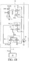
- the present application provides a pixel circuit 10 connected to a signal reading circuit 40, and the signal reading circuit 40 reads a sensing signal of the pixel circuit 10.
- the pixel circuit 10 comprises a light sensing component 11, a reset switch Q1, a transmission switch Q2 and a unity gain buffer 20.
- the reset switch Q1 and transmission switch Q2 are transistors. In this embodiment, both the reset switch Q1 and transmission switch Q2 are NMOS transistors.
- the reset switch Q1 has a drain connected to a first reference voltage VCCR, a gate connected to a reset signal, and a source connected to the drain of transmission switch Q2.
- the transmission switch Q2 has a gate connected to a transmission signal and a source connected to the negative terminal of the light sensing component 11, wherein the positive terminal of the light sensing component 11 is connected to a ground voltage.
- the light sensing component 11 is a photoelectric diode.
- the unity gain buffer 20 has an inverting input terminal (-), a non-inverting input terminal (+) and an output terminal Vout.
- the non-inverting input terminal (+) is connected to a node of connection of the reset switch Q1 and the transmission switch Q2.
- the inverting input terminal (-) of the unity gain buffer 20 is connected to the output terminal Vout, and the output terminal Vout is connected to the signal reading circuit 40.
- the unity gain buffer 20 comprises a non-inverting input circuit 21, an inverting input circuit 22, an active load 23 and a current source 30.
- the non-inverting input circuit 21 comprises the non-inverting input terminal (+); hence, the non-inverting input circuit 21 is connected to a node of connection of transmission switch Q2 and reset switch Q1 through the non-inverting input terminal (+).
- the non-inverting input circuit 21 is connected to the active load 23.
- the inverting input circuit 22 comprises the inverting input terminal (-).
- the active load 23 comprises the output terminal Vout. Therefore, the inverting input terminal (-) of the inverting input circuit 22 is connected to the output terminal Vout of the active load 23.
- the current source 30 is connected to the non-inverting input circuit 21 and the inverting input circuit 22 so as to provide current I.
- the non-inverting input circuit 21 comprises first transistor MN1 and second transistor MN2, wherein both first transistor MN1 and second transistor MN2 are NMOS transistors.
- the gate of first transistor MN1 is connected to a node of connection of transmission switch Q2 and reset switch Q1 through the non-inverting input terminal (+).
- the drain of first transistor MN1 is connected to the active load 23.
- the source of first transistor MN1 is connected to the drain of second transistor MN2.
- the gate of second transistor MN2 is connected to a selection signal.
- the source of second transistor MN2 is connected to the current source 30.
- the inverting input circuit 22 comprises third transistor MN3 and fourth transistor MN4, wherein both third transistor MN3 and fourth transistor MN4 are NMOS transistors.
- the drain and gate of third transistor MN3 are jointly connected to the output terminal Vout of the active load 23 through the inverting input terminal (-).
- the source of third transistor MN3 is connected to the drain of fourth transistor MN4.
- the gate of fourth transistor MN4 is connected to the active load 23.
- the source of fourth transistor MN4 is connected to the current source 30.
- the third transistor MN3 and first transistor MN1 have substantially identical ion implantation so as to generate substantially identical threshold voltage
- the fourth transistor MN4 and second transistor MN2 have substantially identical ion implantation so as to generate substantially identical threshold voltage, so as to match the non-inverting input terminal (+) and the inverting input terminal (-) to a greater extent.
- the active load 23 comprises fifth transistor MP5 and sixth transistor MP6, wherein both fifth transistor MP5 and sixth transistor MP6 are PMOS transistors.
- the gate of fourth transistor MP5 is connected to the gate of sixth transistor MP6.
- the sources of fourth transistor MP5 and sixth transistor MP6 are jointly connected to the gate of fourth transistor MN4 of the inverting input circuit 22.
- the drain of fourth transistor MP5 is connected to the output terminal Vout.
- the drain of sixth transistor MP6 is connected to the gate of sixth transistor MP6 and connected to the drain of first transistor MN1 of the non-inverting input circuit 21.
- the first embodiment of the present application provides an image sensor 1 which comprises a plurality of pixel circuits 10a arranged in a matrix.
- the pixel circuits 10a in each column each comprise a light sensing component 11, a reset switch Q1, a transmission switch Q2 and a non-inverting input circuit 21.
- the pixel circuits 10a in each column share the inverting input circuit 22, the active load 23, and the current source 30.
- the non-inverting input circuit 21 of each of the pixel circuits 10a, the inverting input circuit 22, the active load 23 and the current source 30 equivalently form the unity gain buffer 20.
- the reset switch Q1 is connected to the first reference voltage VCCR.
- the transmission switch Q2 is series-connected between the light sensing component 11 and reset switch Q1.
- the non-inverting input circuit 21 comprises a non-inverting input terminal (+) connected to a node of connection of transmission switch Q2 and reset switch Q1.
- the non-inverting input circuit 21 in FIG. 2 is the same as the non-inverting input circuit 21 in FIG. 1B and therefore is, for the sake of brevity, not described hereunder.
- the inverting input circuit 22 comprises an inverting input terminal (-) and is the same as the inverting input circuit 22 in FIG. 1B and therefore is, for the sake of brevity, not described hereunder.
- the active load 23 comprises the output terminal Vout.
- the output terminal Vout is connected to the inverting input terminal (-).
- the active load 23 is connected to the inverting input circuit 22 and the non-inverting input circuit 21 of each of the pixel circuits 10a.
- the pixel circuits 10a share the inverting input circuit 22 and the active load 23.
- the active load 23 has the same circuit as the active load 23 in FIG. 1B and therefore is, for the sake of brevity, not described hereunder.
- the signal reading circuit 40 is connected to the output terminal Vout of the active load 23 to read the sensing result of the light sensing component 11 of each of the pixel circuits 10a.
- the image sensor 1 comprises a pixel region 100 and a peripheral region 101 defined at the periphery of the pixel region 100.
- the pixel region 100 is surrounded by a pixel region guard ring 102.
- the first transistor MN1 and second transistor MN2 of the non-inverting input circuit 21 and the third transistor MN3 and fourth transistor MN4 of the inverting input circuit 22 are disposed in the pixel region 100 within the pixel region guard ring 102 and undergo the same semiconductor manufacturing process, for example, a doping process, as the transistors, such as reset switch Q1 and transmission switch Q2, within the pixel region guard ring 102, so as to match the non-inverting input circuit 21 and the inverting input circuit 22 to a greater extent.
- the third transistor MN3 and first transistor MN1 have substantially identical ion implantation so as to generate substantially identical threshold voltage
- the fourth transistor MN4 and second transistor MN2 have substantially identical ion implantation so as to generate substantially identical threshold voltage, thereby matching the non-inverting input terminal (+) and the inverting input terminal (-) to a greater extent.
- the fifth transistor MP5 and sixth transistor MP6 of the active load 23 and the signal reading circuit 40 are disposed in the peripheral region 101 outside the pixel region guard ring 102.
- both first transistor MN1 and second transistor MN2 still have a source follower and a selection switch of each of the pixel circuits 10a and are joined by the third through sixth transistors MN3 ⁇ MP6 to form the unity gain buffer 20.
- An output signal of the unity gain buffer 20 varies with an input signal of the unity gain buffer 20, attaining a linear relationship between the output signal and the input signal. Therefore, the photoelectric conversion curve of each of the pixel circuits 10a is linear.
- the second embodiment of the present application provides the image sensor 1a which comprises pixel circuits 10a arranged in a matrix.
- the pixel circuits 10a in each column each comprise a light sensing component 11, a reset switch Q1, a transmission switch Q2 and a non-inverting input circuit 21.
- the image sensor 1a in the second embodiment illustrated by FIG. 3 includes the inverting input circuit 22 in each pixel circuit 10b.
- the pixel circuits 10a in each column share the active load 23 and the current source 30.
- each pixel circuit 10a When each pixel circuit 10a is operating (i.e., when selected by the signal reading circuit 40), the inverting input circuit 22 and the non-inverting input circuit 21 of each pixel circuit 10a together with the active load 23 and the current source 30 equivalently form the unity gain buffer 20.
- the embodiment illustrated by FIG. 3 is characterized in that the image sensor 1 comprises the pixel region 100 surrounded by the pixel region guard ring 102 and the peripheral region 101 defined at the periphery of the pixel region 100.
- the first transistor MN1 and second transistor MN2 of the non-inverting input circuit 21 of each pixel circuit 10a and the third transistor MN3 and fourth transistor MN4 of the inverting input circuit 22 of each pixel circuit 10a are disposed in the pixel region 100 within the pixel region guard ring 102 and undergo the same semiconductor manufacturing process, for example, a doping process, as the transistors, such as reset switch Q1 and transmission switch Q2, within the pixel region guard ring 102, so as to match the non-inverting input circuit 21 and the inverting input circuit 22 to a greater extent.
- the third transistor MN3 and first transistor MN1 have substantially identical ion implantation so as to generate substantially identical threshold voltage
- the fourth transistor MN4 and second transistor MN2 have substantially identical ion implantation so as to generate substantially identical threshold voltage, thereby matching the non-inverting input terminal (+) and the inverting input terminal (-) to a greater extent.
- the fifth transistor MP5 and sixth transistor MP6 of the active load 23 and the signal reading circuit 40 are disposed in the peripheral region 101 outside the pixel region guard ring 102.
- each pixel circuit of the image sensor of the present application is connected to a node of connection of the transmission switch and the reset switch through the unity gain buffer.
- An output signal of the unity gain buffer varies with an input signal of the unity gain buffer, attaining a linear relationship between the output signal and the input signal. Therefore, the photoelectric conversion curve of each pixel circuit is linear.
Landscapes
- Engineering & Computer Science (AREA)
- Multimedia (AREA)
- Signal Processing (AREA)
- Solid State Image Pick-Up Elements (AREA)
- Transforming Light Signals Into Electric Signals (AREA)
Applications Claiming Priority (1)
| Application Number | Priority Date | Filing Date | Title |
|---|---|---|---|
| PCT/CN2018/116318 WO2020102960A1 (zh) | 2018-11-20 | 2018-11-20 | 像素电路及相关影像感测器 |
Publications (3)
| Publication Number | Publication Date |
|---|---|
| EP3678366A1 true EP3678366A1 (de) | 2020-07-08 |
| EP3678366A4 EP3678366A4 (de) | 2020-07-08 |
| EP3678366B1 EP3678366B1 (de) | 2023-03-01 |
Family
ID=66060184
Family Applications (1)
| Application Number | Title | Priority Date | Filing Date |
|---|---|---|---|
| EP18921290.5A Active EP3678366B1 (de) | 2018-11-20 | 2018-11-20 | Pixelschaltung und damit verbundener bildsensor |
Country Status (4)
| Country | Link |
|---|---|
| US (1) | US11310454B2 (de) |
| EP (1) | EP3678366B1 (de) |
| CN (1) | CN109644243B (de) |
| WO (1) | WO2020102960A1 (de) |
Cited By (1)
| Publication number | Priority date | Publication date | Assignee | Title |
|---|---|---|---|---|
| TWI841259B (zh) * | 2023-02-12 | 2024-05-01 | 聯詠科技股份有限公司 | 影像感測裝置 |
Families Citing this family (1)
| Publication number | Priority date | Publication date | Assignee | Title |
|---|---|---|---|---|
| CN110390317B (zh) * | 2019-07-30 | 2024-06-25 | 上海思立微电子科技有限公司 | 像素电路、像素阵列以及光学指纹传感器 |
Family Cites Families (11)
| Publication number | Priority date | Publication date | Assignee | Title |
|---|---|---|---|---|
| US6130423A (en) * | 1998-07-10 | 2000-10-10 | Pixel Cam, Inc. | Method and apparatus for a CMOS image sensor with a distributed amplifier |
| JP3601052B2 (ja) * | 1999-03-11 | 2004-12-15 | 日本電気株式会社 | 固体撮像装置 |
| US6717616B1 (en) * | 1999-08-16 | 2004-04-06 | Intel Corporation | Amplifier assisted active pixel read out structure |
| CN100403771C (zh) * | 2004-05-11 | 2008-07-16 | 凌阳科技股份有限公司 | 影像传感器及其可偏移补偿的参考电压产生电路 |
| US7602429B2 (en) * | 2006-02-01 | 2009-10-13 | Chi Wah Kok | Paired differential active pixel sensor |
| JP5566000B2 (ja) * | 2007-03-12 | 2014-08-06 | キヤノン株式会社 | 発光表示装置の駆動回路、その駆動方法並びにカメラ |
| JP2012048065A (ja) * | 2010-08-27 | 2012-03-08 | Canon Inc | 光電変換装置、焦点検出装置、および撮像システム |
| CN102104744B (zh) * | 2011-03-04 | 2013-01-16 | 北京思比科微电子技术股份有限公司 | Cmos图像传感器像素读出电路结构及像素结构 |
| JP2015115745A (ja) * | 2013-12-11 | 2015-06-22 | ソニー株式会社 | 固体撮像素子、撮像装置、および電子機器 |
| JP2015162751A (ja) * | 2014-02-26 | 2015-09-07 | キヤノン株式会社 | 光電変換装置および撮像システム |
| JP6893325B2 (ja) * | 2016-03-16 | 2021-06-23 | パナソニックIpマネジメント株式会社 | 反転増幅器、積分器、サンプルホールド回路、ad変換器、イメージセンサ、および撮像装置 |
-
2018
- 2018-11-20 CN CN201880002312.2A patent/CN109644243B/zh active Active
- 2018-11-20 EP EP18921290.5A patent/EP3678366B1/de active Active
- 2018-11-20 WO PCT/CN2018/116318 patent/WO2020102960A1/zh not_active Ceased
-
2019
- 2019-12-06 US US16/706,374 patent/US11310454B2/en active Active
Cited By (2)
| Publication number | Priority date | Publication date | Assignee | Title |
|---|---|---|---|---|
| TWI841259B (zh) * | 2023-02-12 | 2024-05-01 | 聯詠科技股份有限公司 | 影像感測裝置 |
| US12532084B2 (en) | 2023-02-12 | 2026-01-20 | Novatek Microelectronics Corp. | Image sensing device |
Also Published As
| Publication number | Publication date |
|---|---|
| EP3678366B1 (de) | 2023-03-01 |
| EP3678366A4 (de) | 2020-07-08 |
| CN109644243B (zh) | 2020-11-24 |
| CN109644243A (zh) | 2019-04-16 |
| WO2020102960A1 (zh) | 2020-05-28 |
| US20200162690A1 (en) | 2020-05-21 |
| US11310454B2 (en) | 2022-04-19 |
Similar Documents
| Publication | Publication Date | Title |
|---|---|---|
| CN108347247B (zh) | 图像传感器 | |
| US6906586B2 (en) | Differential amplifier circuit used in solid-state image pickup apparatus, and arrangement that avoids influence of variations of integrated circuits in manufacture and the like | |
| US11323639B2 (en) | Image sensor and operation method thereof | |
| CN111629161A (zh) | 比较器及包括该比较器的图像感测装置 | |
| CN112753216B (zh) | 摄像元件和光检测器 | |
| CN102650546A (zh) | 光传感器和电子设备 | |
| US11310454B2 (en) | Pixel circuit and image sensor having the same | |
| US9609249B2 (en) | Solid-state imaging device, imaging apparatus, and electronic apparatus with negative feedback circuit | |
| KR100429571B1 (ko) | 저전력화 및 화질 개선을 위한 단위 화소 회로 및 판독 회로를 갖는 이미지센서 | |
| CN113630567B (zh) | 读出电路 | |
| CN114979525A (zh) | 具有有源电容消除电路以减少像素输出稳定时间的图像传感器 | |
| US7064609B1 (en) | High voltage, low-offset operational amplifier with rail-to-rail common mode input range in a digital CMOS process | |
| US11570391B2 (en) | Digitally-calibrated CTIA image sensor pixel | |
| US20220103776A1 (en) | Image sensor amplifiers with reduced inter-circulation currents | |
| US20140070074A1 (en) | Semiconductor integrated circuit and image sensor | |
| US7642860B2 (en) | Current pre-amplifier and associated current comparator | |
| GB2542426A (en) | Pixel circuit | |
| US20150001380A1 (en) | Light receiving circuit | |
| KR20180085349A (ko) | 이미지 센서 | |
| CN116973618A (zh) | 一种电流采样电路 | |
| US11025241B2 (en) | Comparator circuit and mobile device | |
| US10700674B1 (en) | Differential comparator circuit | |
| JP6001887B2 (ja) | 固体撮像装置 | |
| CN107592478B (zh) | 一种三维堆叠图像传感器芯片结构 | |
| JP4797600B2 (ja) | 固体撮像素子の出力バッファ回路およびこれを用いた固体撮像装置 |
Legal Events
| Date | Code | Title | Description |
|---|---|---|---|
| STAA | Information on the status of an ep patent application or granted ep patent |
Free format text: STATUS: UNKNOWN |
|
| STAA | Information on the status of an ep patent application or granted ep patent |
Free format text: STATUS: THE INTERNATIONAL PUBLICATION HAS BEEN MADE |
|
| PUAI | Public reference made under article 153(3) epc to a published international application that has entered the european phase |
Free format text: ORIGINAL CODE: 0009012 |
|
| STAA | Information on the status of an ep patent application or granted ep patent |
Free format text: STATUS: REQUEST FOR EXAMINATION WAS MADE |
|
| 17P | Request for examination filed |
Effective date: 20191210 |
|
| A4 | Supplementary search report drawn up and despatched |
Effective date: 20200608 |
|
| AK | Designated contracting states |
Kind code of ref document: A1 Designated state(s): AL AT BE BG CH CY CZ DE DK EE ES FI FR GB GR HR HU IE IS IT LI LT LU LV MC MK MT NL NO PL PT RO RS SE SI SK SM TR |
|
| AX | Request for extension of the european patent |
Extension state: BA ME |
|
| STAA | Information on the status of an ep patent application or granted ep patent |
Free format text: STATUS: EXAMINATION IS IN PROGRESS |
|
| 17Q | First examination report despatched |
Effective date: 20211207 |
|
| DAV | Request for validation of the european patent (deleted) | ||
| DAX | Request for extension of the european patent (deleted) | ||
| GRAP | Despatch of communication of intention to grant a patent |
Free format text: ORIGINAL CODE: EPIDOSNIGR1 |
|
| STAA | Information on the status of an ep patent application or granted ep patent |
Free format text: STATUS: GRANT OF PATENT IS INTENDED |
|
| INTG | Intention to grant announced |
Effective date: 20220928 |
|
| RIN1 | Information on inventor provided before grant (corrected) |
Inventor name: CHAO, WEI-MIN Inventor name: TSENG, CHIEN-JIAN |
|
| GRAS | Grant fee paid |
Free format text: ORIGINAL CODE: EPIDOSNIGR3 |
|
| GRAA | (expected) grant |
Free format text: ORIGINAL CODE: 0009210 |
|
| STAA | Information on the status of an ep patent application or granted ep patent |
Free format text: STATUS: THE PATENT HAS BEEN GRANTED |
|
| AK | Designated contracting states |
Kind code of ref document: B1 Designated state(s): AL AT BE BG CH CY CZ DE DK EE ES FI FR GB GR HR HU IE IS IT LI LT LU LV MC MK MT NL NO PL PT RO RS SE SI SK SM TR |
|
| REG | Reference to a national code |
Ref country code: GB Ref legal event code: FG4D |
|
| REG | Reference to a national code |
Ref country code: CH Ref legal event code: EP Ref country code: AT Ref legal event code: REF Ref document number: 1551829 Country of ref document: AT Kind code of ref document: T Effective date: 20230315 |
|
| REG | Reference to a national code |
Ref country code: DE Ref legal event code: R096 Ref document number: 602018046845 Country of ref document: DE |
|
| REG | Reference to a national code |
Ref country code: IE Ref legal event code: FG4D |
|
| REG | Reference to a national code |
Ref country code: LT Ref legal event code: MG9D |
|
| REG | Reference to a national code |
Ref country code: NL Ref legal event code: MP Effective date: 20230301 |
|
| PG25 | Lapsed in a contracting state [announced via postgrant information from national office to epo] |
Ref country code: RS Free format text: LAPSE BECAUSE OF FAILURE TO SUBMIT A TRANSLATION OF THE DESCRIPTION OR TO PAY THE FEE WITHIN THE PRESCRIBED TIME-LIMIT Effective date: 20230301 Ref country code: NO Free format text: LAPSE BECAUSE OF FAILURE TO SUBMIT A TRANSLATION OF THE DESCRIPTION OR TO PAY THE FEE WITHIN THE PRESCRIBED TIME-LIMIT Effective date: 20230601 Ref country code: LV Free format text: LAPSE BECAUSE OF FAILURE TO SUBMIT A TRANSLATION OF THE DESCRIPTION OR TO PAY THE FEE WITHIN THE PRESCRIBED TIME-LIMIT Effective date: 20230301 Ref country code: LT Free format text: LAPSE BECAUSE OF FAILURE TO SUBMIT A TRANSLATION OF THE DESCRIPTION OR TO PAY THE FEE WITHIN THE PRESCRIBED TIME-LIMIT Effective date: 20230301 Ref country code: HR Free format text: LAPSE BECAUSE OF FAILURE TO SUBMIT A TRANSLATION OF THE DESCRIPTION OR TO PAY THE FEE WITHIN THE PRESCRIBED TIME-LIMIT Effective date: 20230301 Ref country code: ES Free format text: LAPSE BECAUSE OF FAILURE TO SUBMIT A TRANSLATION OF THE DESCRIPTION OR TO PAY THE FEE WITHIN THE PRESCRIBED TIME-LIMIT Effective date: 20230301 |
|
| REG | Reference to a national code |
Ref country code: AT Ref legal event code: MK05 Ref document number: 1551829 Country of ref document: AT Kind code of ref document: T Effective date: 20230301 |
|
| PG25 | Lapsed in a contracting state [announced via postgrant information from national office to epo] |
Ref country code: SE Free format text: LAPSE BECAUSE OF FAILURE TO SUBMIT A TRANSLATION OF THE DESCRIPTION OR TO PAY THE FEE WITHIN THE PRESCRIBED TIME-LIMIT Effective date: 20230301 Ref country code: PL Free format text: LAPSE BECAUSE OF FAILURE TO SUBMIT A TRANSLATION OF THE DESCRIPTION OR TO PAY THE FEE WITHIN THE PRESCRIBED TIME-LIMIT Effective date: 20230301 Ref country code: NL Free format text: LAPSE BECAUSE OF FAILURE TO SUBMIT A TRANSLATION OF THE DESCRIPTION OR TO PAY THE FEE WITHIN THE PRESCRIBED TIME-LIMIT Effective date: 20230301 Ref country code: GR Free format text: LAPSE BECAUSE OF FAILURE TO SUBMIT A TRANSLATION OF THE DESCRIPTION OR TO PAY THE FEE WITHIN THE PRESCRIBED TIME-LIMIT Effective date: 20230602 Ref country code: FI Free format text: LAPSE BECAUSE OF FAILURE TO SUBMIT A TRANSLATION OF THE DESCRIPTION OR TO PAY THE FEE WITHIN THE PRESCRIBED TIME-LIMIT Effective date: 20230301 |
|
| PG25 | Lapsed in a contracting state [announced via postgrant information from national office to epo] |
Ref country code: SM Free format text: LAPSE BECAUSE OF FAILURE TO SUBMIT A TRANSLATION OF THE DESCRIPTION OR TO PAY THE FEE WITHIN THE PRESCRIBED TIME-LIMIT Effective date: 20230301 Ref country code: RO Free format text: LAPSE BECAUSE OF FAILURE TO SUBMIT A TRANSLATION OF THE DESCRIPTION OR TO PAY THE FEE WITHIN THE PRESCRIBED TIME-LIMIT Effective date: 20230301 Ref country code: PT Free format text: LAPSE BECAUSE OF FAILURE TO SUBMIT A TRANSLATION OF THE DESCRIPTION OR TO PAY THE FEE WITHIN THE PRESCRIBED TIME-LIMIT Effective date: 20230703 Ref country code: EE Free format text: LAPSE BECAUSE OF FAILURE TO SUBMIT A TRANSLATION OF THE DESCRIPTION OR TO PAY THE FEE WITHIN THE PRESCRIBED TIME-LIMIT Effective date: 20230301 Ref country code: CZ Free format text: LAPSE BECAUSE OF FAILURE TO SUBMIT A TRANSLATION OF THE DESCRIPTION OR TO PAY THE FEE WITHIN THE PRESCRIBED TIME-LIMIT Effective date: 20230301 Ref country code: AT Free format text: LAPSE BECAUSE OF FAILURE TO SUBMIT A TRANSLATION OF THE DESCRIPTION OR TO PAY THE FEE WITHIN THE PRESCRIBED TIME-LIMIT Effective date: 20230301 |
|
| PG25 | Lapsed in a contracting state [announced via postgrant information from national office to epo] |
Ref country code: SK Free format text: LAPSE BECAUSE OF FAILURE TO SUBMIT A TRANSLATION OF THE DESCRIPTION OR TO PAY THE FEE WITHIN THE PRESCRIBED TIME-LIMIT Effective date: 20230301 Ref country code: IS Free format text: LAPSE BECAUSE OF FAILURE TO SUBMIT A TRANSLATION OF THE DESCRIPTION OR TO PAY THE FEE WITHIN THE PRESCRIBED TIME-LIMIT Effective date: 20230701 |
|
| REG | Reference to a national code |
Ref country code: DE Ref legal event code: R097 Ref document number: 602018046845 Country of ref document: DE |
|
| PLBE | No opposition filed within time limit |
Free format text: ORIGINAL CODE: 0009261 |
|
| STAA | Information on the status of an ep patent application or granted ep patent |
Free format text: STATUS: NO OPPOSITION FILED WITHIN TIME LIMIT |
|
| PG25 | Lapsed in a contracting state [announced via postgrant information from national office to epo] |
Ref country code: SI Free format text: LAPSE BECAUSE OF FAILURE TO SUBMIT A TRANSLATION OF THE DESCRIPTION OR TO PAY THE FEE WITHIN THE PRESCRIBED TIME-LIMIT Effective date: 20230301 Ref country code: DK Free format text: LAPSE BECAUSE OF FAILURE TO SUBMIT A TRANSLATION OF THE DESCRIPTION OR TO PAY THE FEE WITHIN THE PRESCRIBED TIME-LIMIT Effective date: 20230301 |
|
| 26N | No opposition filed |
Effective date: 20231204 |
|
| PG25 | Lapsed in a contracting state [announced via postgrant information from national office to epo] |
Ref country code: IT Free format text: LAPSE BECAUSE OF FAILURE TO SUBMIT A TRANSLATION OF THE DESCRIPTION OR TO PAY THE FEE WITHIN THE PRESCRIBED TIME-LIMIT Effective date: 20230301 |
|
| REG | Reference to a national code |
Ref country code: CH Ref legal event code: PL |
|
| PG25 | Lapsed in a contracting state [announced via postgrant information from national office to epo] |
Ref country code: MC Free format text: LAPSE BECAUSE OF FAILURE TO SUBMIT A TRANSLATION OF THE DESCRIPTION OR TO PAY THE FEE WITHIN THE PRESCRIBED TIME-LIMIT Effective date: 20230301 |
|
| PG25 | Lapsed in a contracting state [announced via postgrant information from national office to epo] |
Ref country code: LU Free format text: LAPSE BECAUSE OF NON-PAYMENT OF DUE FEES Effective date: 20231120 |
|
| PG25 | Lapsed in a contracting state [announced via postgrant information from national office to epo] |
Ref country code: CH Free format text: LAPSE BECAUSE OF NON-PAYMENT OF DUE FEES Effective date: 20231130 |
|
| PG25 | Lapsed in a contracting state [announced via postgrant information from national office to epo] |
Ref country code: MC Free format text: LAPSE BECAUSE OF FAILURE TO SUBMIT A TRANSLATION OF THE DESCRIPTION OR TO PAY THE FEE WITHIN THE PRESCRIBED TIME-LIMIT Effective date: 20230301 Ref country code: LU Free format text: LAPSE BECAUSE OF NON-PAYMENT OF DUE FEES Effective date: 20231120 Ref country code: CH Free format text: LAPSE BECAUSE OF NON-PAYMENT OF DUE FEES Effective date: 20231130 |
|
| REG | Reference to a national code |
Ref country code: BE Ref legal event code: MM Effective date: 20231130 |
|
| REG | Reference to a national code |
Ref country code: IE Ref legal event code: MM4A |
|
| PG25 | Lapsed in a contracting state [announced via postgrant information from national office to epo] |
Ref country code: IE Free format text: LAPSE BECAUSE OF NON-PAYMENT OF DUE FEES Effective date: 20231120 |
|
| PG25 | Lapsed in a contracting state [announced via postgrant information from national office to epo] |
Ref country code: BE Free format text: LAPSE BECAUSE OF NON-PAYMENT OF DUE FEES Effective date: 20231130 |
|
| PG25 | Lapsed in a contracting state [announced via postgrant information from national office to epo] |
Ref country code: FR Free format text: LAPSE BECAUSE OF NON-PAYMENT OF DUE FEES Effective date: 20231130 |
|
| PG25 | Lapsed in a contracting state [announced via postgrant information from national office to epo] |
Ref country code: IE Free format text: LAPSE BECAUSE OF NON-PAYMENT OF DUE FEES Effective date: 20231120 Ref country code: FR Free format text: LAPSE BECAUSE OF NON-PAYMENT OF DUE FEES Effective date: 20231130 Ref country code: BE Free format text: LAPSE BECAUSE OF NON-PAYMENT OF DUE FEES Effective date: 20231130 |
|
| PG25 | Lapsed in a contracting state [announced via postgrant information from national office to epo] |
Ref country code: BG Free format text: LAPSE BECAUSE OF FAILURE TO SUBMIT A TRANSLATION OF THE DESCRIPTION OR TO PAY THE FEE WITHIN THE PRESCRIBED TIME-LIMIT Effective date: 20230301 |
|
| PG25 | Lapsed in a contracting state [announced via postgrant information from national office to epo] |
Ref country code: BG Free format text: LAPSE BECAUSE OF FAILURE TO SUBMIT A TRANSLATION OF THE DESCRIPTION OR TO PAY THE FEE WITHIN THE PRESCRIBED TIME-LIMIT Effective date: 20230301 |
|
| PG25 | Lapsed in a contracting state [announced via postgrant information from national office to epo] |
Ref country code: CY Free format text: LAPSE BECAUSE OF FAILURE TO SUBMIT A TRANSLATION OF THE DESCRIPTION OR TO PAY THE FEE WITHIN THE PRESCRIBED TIME-LIMIT; INVALID AB INITIO Effective date: 20181120 |
|
| PG25 | Lapsed in a contracting state [announced via postgrant information from national office to epo] |
Ref country code: HU Free format text: LAPSE BECAUSE OF FAILURE TO SUBMIT A TRANSLATION OF THE DESCRIPTION OR TO PAY THE FEE WITHIN THE PRESCRIBED TIME-LIMIT; INVALID AB INITIO Effective date: 20181120 |
|
| PG25 | Lapsed in a contracting state [announced via postgrant information from national office to epo] |
Ref country code: TR Free format text: LAPSE BECAUSE OF FAILURE TO SUBMIT A TRANSLATION OF THE DESCRIPTION OR TO PAY THE FEE WITHIN THE PRESCRIBED TIME-LIMIT Effective date: 20230301 |
|
| PGFP | Annual fee paid to national office [announced via postgrant information from national office to epo] |
Ref country code: DE Payment date: 20251111 Year of fee payment: 8 |
|
| PGFP | Annual fee paid to national office [announced via postgrant information from national office to epo] |
Ref country code: GB Payment date: 20251114 Year of fee payment: 8 |