EP3671293A1 - An optical device comprising at least one diffraction grating having a grating pitch above the wavelength - Google Patents
An optical device comprising at least one diffraction grating having a grating pitch above the wavelength Download PDFInfo
- Publication number
- EP3671293A1 EP3671293A1 EP18215212.4A EP18215212A EP3671293A1 EP 3671293 A1 EP3671293 A1 EP 3671293A1 EP 18215212 A EP18215212 A EP 18215212A EP 3671293 A1 EP3671293 A1 EP 3671293A1
- Authority
- EP
- European Patent Office
- Prior art keywords
- diffraction grating
- refractive index
- diffraction
- light
- optical device
- Prior art date
- Legal status (The legal status is an assumption and is not a legal conclusion. Google has not performed a legal analysis and makes no representation as to the accuracy of the status listed.)
- Withdrawn
Links
- 230000003287 optical effect Effects 0.000 title claims abstract description 77
- 239000000758 substrate Substances 0.000 claims description 38
- 239000003989 dielectric material Substances 0.000 claims description 33
- 238000010168 coupling process Methods 0.000 claims description 17
- 238000005859 coupling reaction Methods 0.000 claims description 17
- 230000005855 radiation Effects 0.000 claims description 11
- 230000008878 coupling Effects 0.000 claims description 6
- 239000000463 material Substances 0.000 description 49
- 238000009826 distribution Methods 0.000 description 39
- 239000011521 glass Substances 0.000 description 24
- 238000009304 pastoral farming Methods 0.000 description 13
- 238000000605 extraction Methods 0.000 description 10
- 238000013461 design Methods 0.000 description 9
- 230000009977 dual effect Effects 0.000 description 9
- 238000004519 manufacturing process Methods 0.000 description 8
- 238000004458 analytical method Methods 0.000 description 6
- 238000000034 method Methods 0.000 description 6
- 230000001902 propagating effect Effects 0.000 description 5
- 210000001747 pupil Anatomy 0.000 description 5
- 230000004044 response Effects 0.000 description 5
- 230000008569 process Effects 0.000 description 4
- 230000008901 benefit Effects 0.000 description 3
- 230000008859 change Effects 0.000 description 3
- 238000000609 electron-beam lithography Methods 0.000 description 3
- 238000005530 etching Methods 0.000 description 3
- 230000006872 improvement Effects 0.000 description 3
- 230000000737 periodic effect Effects 0.000 description 3
- 239000000243 solution Substances 0.000 description 3
- 238000012546 transfer Methods 0.000 description 3
- 230000004075 alteration Effects 0.000 description 2
- 230000001066 destructive effect Effects 0.000 description 2
- 230000000694 effects Effects 0.000 description 2
- 238000005516 engineering process Methods 0.000 description 2
- 238000001459 lithography Methods 0.000 description 2
- 208000032366 Oversensing Diseases 0.000 description 1
- 229910052581 Si3N4 Inorganic materials 0.000 description 1
- 230000003190 augmentative effect Effects 0.000 description 1
- 230000005540 biological transmission Effects 0.000 description 1
- 238000011161 development Methods 0.000 description 1
- 238000003384 imaging method Methods 0.000 description 1
- 238000002347 injection Methods 0.000 description 1
- 239000007924 injection Substances 0.000 description 1
- 230000010287 polarization Effects 0.000 description 1
- 230000009467 reduction Effects 0.000 description 1
- 238000011160 research Methods 0.000 description 1
- HQVNEWCFYHHQES-UHFFFAOYSA-N silicon nitride Chemical compound N12[Si]34N5[Si]62N3[Si]51N64 HQVNEWCFYHHQES-UHFFFAOYSA-N 0.000 description 1
- 238000004088 simulation Methods 0.000 description 1
- 239000012780 transparent material Substances 0.000 description 1
Images


Classifications
-
- G—PHYSICS
- G02—OPTICS
- G02B—OPTICAL ELEMENTS, SYSTEMS OR APPARATUS
- G02B5/00—Optical elements other than lenses
- G02B5/18—Diffraction gratings
- G02B5/1866—Transmission gratings characterised by their structure, e.g. step profile, contours of substrate or grooves, pitch variations, materials
-
- G—PHYSICS
- G02—OPTICS
- G02B—OPTICAL ELEMENTS, SYSTEMS OR APPARATUS
- G02B27/00—Optical systems or apparatus not provided for by any of the groups G02B1/00 - G02B26/00, G02B30/00
- G02B27/0081—Optical systems or apparatus not provided for by any of the groups G02B1/00 - G02B26/00, G02B30/00 with means for altering, e.g. enlarging, the entrance or exit pupil
-
- G—PHYSICS
- G02—OPTICS
- G02B—OPTICAL ELEMENTS, SYSTEMS OR APPARATUS
- G02B27/00—Optical systems or apparatus not provided for by any of the groups G02B1/00 - G02B26/00, G02B30/00
- G02B27/01—Head-up displays
- G02B27/017—Head mounted
- G02B27/0172—Head mounted characterised by optical features
-
- G—PHYSICS
- G02—OPTICS
- G02B—OPTICAL ELEMENTS, SYSTEMS OR APPARATUS
- G02B5/00—Optical elements other than lenses
- G02B5/18—Diffraction gratings
- G02B5/1814—Diffraction gratings structurally combined with one or more further optical elements, e.g. lenses, mirrors, prisms or other diffraction gratings
-
- G—PHYSICS
- G02—OPTICS
- G02B—OPTICAL ELEMENTS, SYSTEMS OR APPARATUS
- G02B27/00—Optical systems or apparatus not provided for by any of the groups G02B1/00 - G02B26/00, G02B30/00
- G02B27/01—Head-up displays
- G02B27/0101—Head-up displays characterised by optical features
- G02B2027/0112—Head-up displays characterised by optical features comprising device for genereting colour display
-
- G—PHYSICS
- G02—OPTICS
- G02B—OPTICAL ELEMENTS, SYSTEMS OR APPARATUS
- G02B27/00—Optical systems or apparatus not provided for by any of the groups G02B1/00 - G02B26/00, G02B30/00
- G02B27/01—Head-up displays
- G02B27/0101—Head-up displays characterised by optical features
- G02B2027/0123—Head-up displays characterised by optical features comprising devices increasing the field of view
-
- G—PHYSICS
- G02—OPTICS
- G02B—OPTICAL ELEMENTS, SYSTEMS OR APPARATUS
- G02B27/00—Optical systems or apparatus not provided for by any of the groups G02B1/00 - G02B26/00, G02B30/00
- G02B27/01—Head-up displays
- G02B27/017—Head mounted
- G02B2027/0178—Eyeglass type
Definitions
- the present disclosure relates to the field of optics and photonics, and more specifically to optical device comprising at least one diffraction grating. It may find applications in the field of conformable and wearable optics (i.e. AR/VR glasses (Augmented Reality/Virtual Reality)), as well as in a variety of other electronic consumer products comprising displays and/or lightweight imaging systems.
- conformable and wearable optics i.e. AR/VR glasses (Augmented Reality/Virtual Reality)
- AR/VR glasses are considered as the next generation human-machine interface, thus raising significant interest of major industrial players in the domain of consumer electronics and mobile devices.
- AR/VR glasses and more generally eyewear electronic devices
- development of AR/VR glasses is associated with a number of challenges, including reduction of size and weight of such devices as well as improvement of the image quality (in terms of contrast, field of view, color depth, etc.) that should be realistic enough to enable a truly immersive user experience.
- optical components The tradeoff between the image quality and physical size of the optical components motivates research into ultra-compact optical components that can be used as building blocks for more complex optical systems, such as AR/VR glasses. Such optical components shall also be easy to fabricate and replicate.
- various types of refractive and diffractive lenses and beam-forming components are used to guide the light from a micro-display or a projector towards the human eye, allowing forming a virtual image that is superimposed with an image of the physical world seen with a naked eye (in case of AR glasses) or captured by a camera (in case of VR glasses).
- Some of kind of AR/VR glasses utilizes optical waveguide wherein light propagates into the optical waveguide by TIR (for Total Internal Reflection) only over a limited range of internal angles.
- TIR Total Internal Reflection
- the FoV for Field of View
- the material of the waveguide depends on the material of the waveguide.
- the FoV of a waveguide is defined as the maximum span of ⁇ 1 + ⁇ ⁇ 1 ⁇ which propagates into the waveguide by TIR.
- the biggest angular span that can be coupled into the waveguide is defined by two rays: the ray critical ( ⁇ 1 C in figure 1A ) having incident angle ⁇ 1 C and the grazing ray ( ⁇ 1 G . in figure 1A ) having incident angle ⁇ 1 G .
- the theoretical FoV of a waveguide presented above is for a single mode system where one single diffraction mode is used to carry the image: either +1 or -1 diffraction mode.
- WO2017180403 a waveguide with extended Field of View is proposed wherein a dual mode image propagation is used. In this method, they use the diffraction mode +1 to carry the right hand side image (negative angles of incidence on the incoupler) in one direction and the -1 mode to propagate the positive angles of incidence into the opposite direction into the waveguide. Such a system is illustrated by figure 1B wherein critical angle and grazing angle are shown for both diffraction modes.
- combining both half images is done thanks to the pupil expanders and out-couplers at the exit of the waveguide so that the user sees one single image. The benefit of the system is to double the Field of View since each half image can use the whole angular bandwidth of the waveguide in each direction of propagation.
- d 2 ⁇ ⁇ n 2 + 1 (Eq. 1)
- Equation 1 in any case implies that the diffraction grating has a sub-wavelength structure.
- a waveguide for eye glasses is disclosed wherein the grating's pitch of the structure is between 250 and 500nm.
- An optical device comprising at least one diffraction grating, wherein said at least one diffraction grating is configured to diffract a light of at least one given wavelength incident on said optical device, wherein said at least one diffraction grating has a grating pitch above said at least one given wavelength and wherein said at least one diffraction grating is configured to diffract said incident light at a diffraction order having an absolute value equal to or greater than 2, wherein the optical device is an optical waveguide configured for guiding said light diffracted at a diffraction order having an absolute value equal to or greater than 2.
- the diffraction grating is dedicated to a given wavelength or a group of given wavelengths.
- the diffraction grating is configured so that main part of incident light is diffracted at a diffraction order having an absolute value equal to or greater than 2.
- > 1 with M being the diffraction order, has the effect of multiplying the wavelength by the order which is used in the diffraction equation.
- M ⁇ As the grating pitch is directly a function of the product M ⁇ , this means that the grating pitch is multiplied by M and the structures used for the in-coupler are much bigger. This opens up new possibilities in the fabrication technology, because nano-imprinting could be used. We also get less lines per mm for the grating density and the fabrication process can be optimized since the structures will no more be sub-wavelength but over-wavelength.
- the diffraction grating has thus over-wavelength structures which put less constrains on fabrication than sub-wavelength structures.
- said at least one diffraction grating comprises a base pattern comprising at least one dielectric material, said base pattern being configured to form a nanojet beam associated with edges of the base pattern from said light incident on said at least one diffraction grating.
- nanojet beam forming phenomenon is exploited for transferring energy of main part of incident light into second order diffraction beams.
- the use of a base pattern configured to form nanojet beams from the edges of the base pattern allows to provide high diffraction efficiency while at the same time providing high diffraction uniformity.
- Prior art system do not work with higher order diffraction because configuration of prior art system provides diffraction efficiency close to 0.
- the use of a base pattern configured to form nanojet beams allows to achieve high diffraction efficiency, the diffraction uniformity is average and at least equal to what prior art systems produce with lower diffraction orders.
- said at least one diffraction grating comprises at least one dielectric material with refractive index n 2 deposited on a substrate with refractive index n 3 , and n 3 ⁇ n 2 .
- said base pattern of said at least one diffraction grating is configured according to at least any one of the following arrangements:
- said base pattern comprises two blocks of dielectric material with refractive index n 2 having identical dimensions, on top of said substrate, said two blocks being placed at a determined distance W 1
- said two blocks have a height H 2 with H 2 ⁇ W 2 tan ⁇ B 1 and H 2 ⁇ W 2 tan ⁇ B 1 with W 2 being the width of each of the two blocks and ⁇ ' B 1 and ⁇ " B 1 being respective angles of nanojet beams radiationassociated with edges of the base pattern from said light incident on said at least one diffraction grating, wherein ⁇ B 1 ⁇ ⁇ B 1 ⁇ ⁇ i 2 , ⁇ B 1 ⁇ ⁇ B 1 + ⁇ i 2 with ⁇ i being the angle of the incident light with respect to a normal to the top surface of said diffraction grating and ⁇ B 1 ⁇ 90 ° ⁇ sin ⁇ 1 n 1 n 2 2 , n 1 being the refractive index of host medium in which the d
- said base pattern comprises one block of said dielectric material with refractive index n 2 on top of said substrate, having a U shape, said U-shape consisting in two blocks of height H 2 and width W 2 separated by a central block of height H 1 , with H 1 lower than H 2 , and H 2 ⁇ H 1 ⁇ W 2 tan ⁇ B 1 with ⁇ B 1 ⁇ ⁇ B 1 ⁇ ⁇ i 2 with ⁇ i being the angle of the incident light with respect to a normal to the top surface of said diffraction grating and ⁇ B 1 ⁇ 90 ° ⁇ sin ⁇ 1 n 1 n 2 2 , n 1 being the refractive index of host medium in which the diffraction grating is placed.
- W 1 being said determined distance or a width of said central block
- W 2 being the width of each of said two blocks or of each of said two lobes
- W 1 and W 2 depend on a grating pitch d of said diffraction grating with W 1 ⁇ d 3 and W 1 + W 2 ⁇ d 2 .
- said base pattern has a symmetric geometry.
- the optical device can be used in dual mode. For instance, it can be implemented in a waveguide which separates right hand side and left hand side of an input image to double the Field of View of the waveguide.
- said base pattern has an asymmetric geometry.
- the optical device is designd for single mode diffraction, for instance for in-coupler that just deviates the image into a signel side of a waveguide. This embodiment allows to have even bigger grating's pitch.
- said at least one diffraction grating is configured to diffract light for a group of wavelengths comprising more than one wavelength, and wherein said grating pitch is above the highest wavelength of said group of wavelengths.
- the optical device comprises one diffraction grating per Red, Green and Blue color.
- the optical device is an optical waveguide.
- the optical device can advantageously be used as a waveguide, for instance a waveguide for AR/VR glasses.
- said at least one diffraction grating is configured for in-coupling light incoming into said optical waveguide or for extracting light out of said optical waveguide.
- said at least one diffraction grating is configured for in-coupling light incoming into said optical waveguide and wherein said optical waveguide comprises another diffraction grating configured for extracting light out of said optical waveguide, said other diffraction grating having a grating pitch above a wavelength of said light and said other diffraction grating being configured to diffract said light at a diffraction order having an absolute value equal to or greater than 2.
- an eyewear apparatus comprises at least one optical device according to any one of the embodiments discsussed above.
- the eyewear apparatus comprises:
- an optical device comprising at least one diffraction grating
- such an optical device can be used as a waveguide for AR/VR glasses for instance.
- the optical device presents a specific diffraction grating that can be used for in coupling light into the optical device and /or out coupling light from the optical device.
- the diffraction grating is configured to diffract an incident light at a diffraction order having an absolute value equal to or greater than 2.
- Figure 2 shows schematically what happens to a plane wave (PW) incident upon a linear grating (DG).
- the plane wave gets divided into diffraction modes (-2, -1, 0, +1, +2), which are angular spaced beams of local maximum intensity.
- the diffracted modes number -2,-1,0, 1 and 2 are represented but higher orders exist.
- the order zero has in general the more power and is the natural mode into which the regular refraction or reflection would occur. We might also have diffracted modes in reflection.
- a grating In general, a grating generates a lot of diffraction orders. In numerous applications it is wishful to kill all other modes but the first one.
- An example of such gratings are thick holograms made by the interference of two plane waves.
- n 2 ⁇ sin ⁇ 2 ⁇ n 1 ⁇ sin ⁇ 1 M ⁇ T .
- n 1 ( ⁇ ) and n 2 ( ⁇ ) are the index of refraction of the incident and diffracted media respectively.
- n 1 ( ⁇ ) 1.
- ⁇ 1 is the incident angle
- ⁇ 2 the diffracted angle
- M is the diffraction order
- ⁇ the wavelength
- T the grating frequency
- the light engine consists in light sources and one display.
- the light sources are power LED that are time sequentially driven and the design of the flat optics shall be adapted to the wavelengths of the LEDs.
- Example of common LEDs for near to eye projection are: Blue 459nm True Green 530nm Red 625nm
- the diffraction process is very dispersive. The diffraction angle is different for different wavelength as it varies linearly with the wavelength (M ⁇ T) which is quite a big variation. It is therefore necessary to find a mean to minimize chromatic aberrations.
- One way of handling this is to have one waveguide per color band as the diffraction grating needs to be different for each one. So if we are dealing with an RGB true color image, we would need to have three waveguides. This complicates their design.
- Figure 3 shows the definition of some important rays used to characterize a waveguide.
- Capital superscript letters and indicate respectively the grazing and critical rays. If the subscript is 1, the rays are outside of the waveguide, if it is 2, they are inside.
- the maximal input angular bandwidth of the grating from the figure is ⁇ 1 C ⁇ 1 G and the maximal waveguides angular bandwidth is ⁇ 2 C ⁇ 2 G . This being said, the ray ⁇ 2 G is not a wishful option, as it is not possible to extract that ray.
- the angular bandwidth inside of the waveguide will be limited to ⁇ 2 C ⁇ 2 G ⁇ ⁇ 2 C ⁇ 2 G , (the angular sector indicated by ABDW on figure 3 ) which correspond to the input angular range ⁇ 1 C ⁇ 1 G ⁇ ⁇ 1 C ⁇ 1 G .
- Concerning angular sign convention the positive angle measure is oriented in the trigonometrical direction, which means that ⁇ 1 G > 0 and all other ⁇ 1 x ⁇ 0 on the figure.
- the diffracted rays on the figure have all positive values and the diffraction mode is a positive one, M > 0.
- the extraction port is an even number. If we denote x i C,G the distance from an input of a critical ray or grazing ray before he bounce number i, i is called the extraction port. If i is even, the extraction port is on the same side than the light engine and if i is odd the extraction port is on the opposite side of the light engine.
- a way of using practically this definition of extraction port is to set a diffraction grating between the points [x 2 C , x 2 G ] whose result would be to gather the image out of the waveguide by diffraction between those two points.
- the image is said to be extracted at port number 2.
- the maximal angular span of the input beam for negative angles is ⁇ 1 C ⁇ 1 G which couples into the waveguide to span the angular bandwidth of ⁇ 2 C ⁇ 2 G .
- the grating's pitch will be greater and we could avoid to be on the very limits of the micro fabrication processes.
- the table 2 shows the difference between a grating designed to couple second orders and a grating for first orders.
- the difference in pitch size is almost doubled.
- the grating (using second diffraction order) are called over-wavelength gratings as their pitch is always bigger than the wavelength of the color band they are designed for.
- the grating (using first diffraction order) can be called subwavelength gratings since their pitch is smaller than the wavelength of the color band they are designed for.
- the field of view from the table 2 is given for a system that uses both ⁇ 2 diffraction orders. It is twice the field of view of previous systems working in only one direction into the waveguide.
- the nanojet based diffraction gratings disclosed herein allows to get symmetric response into ⁇ 2 diffraction orders with also very high diffraction uniformity, which is a real strength.
- Figures 4A and 4B illustrates an exemplary schematic light engine providing a 60° field of view.
- the light engine comprises a display emitting incoming light to a set of optics that couple incoming light to an exit pupil placed at the last surface after the last lens of the set of optics, where the rays intersect into the smallest circular cross section.
- the diffraction grating is to be placed there.
- On figure 4A we can see only rays of negative incident angle onto the in-coupling grating (exit pupil). Those rays come from the upper part of the display.
- On figure 4B we can see only rays of positive incident angle onto the in-coupling grating (exit pupil). Those rays come from the lower part of the display.
- Figure 5 shows the light engine from figures 4A and 4B with the waveguide (WG) provided with the in-coupling grating.
- Figure 5 is a schematic view of the light engine obtained from simulation. Only incoupling of incoming light into the waveguide is shown. On the simulated view, light rays are not extracted at output using extraction ports.
- n 1 is the refractive index of host medium
- n 2 represents the refractive index of the high index material
- n 3 represents a lower refractive index, most of the time the glass substrate's index.
- FIG. 6 An exemplary geometry for a base pattern of a diffraction grating configured to diffract light at a diffraction order having an absolute value equal to or greater than 2 is disclosed in figure 6 .
- the base pattern comprises two dieletric materials: a block ME2 of dielectric material with refractive index n 2 placed on top of a layer ME3 of dieletric material with refractive index n 3 .
- the layer ME3 presents a block B3 of same dielectric material, the block B3 is inserted in block ME2.
- Other slightly varying parameters could be used for a variable aspect of the diffraction curves.
- This structure is symmetrical, as it needs to feed a positive and a negative diffraction order in a symmetric way.
- a glass etching is first needed to generate the first structure (layer ME3) into the waveguide's base material. Then an ebeam lithography resist in spin coated on top of the structure and again exposed and etched to add the second component (ME2 block).
- Both ME2 and ME3 components are dielectric transparent materials. This structure, as can be seen from the dimensions illustrated on figure 6 , has a much bigger pitch than in the prior art: 822.4nm instead of 496nm.
- the aspect ratio is of 700/460 ⁇ 1.5 which is a low one, the depth is not much bigger than the width.
- Figure 7 illustrates the diffraction performances of the grating illustrated on figure 6 .
- Order 0,+1 and -1 do not couple into the waveguide, they transmit through and will not reduce the virtual image
- Figure 8 illustrates the diffraction performances of the grating structure of figure 6 but without the high index material (ME2). As can be seen on figure 8 , the diffraction efficiency of +2 and -2 orders in that case are marginal.
- Second couple of NJs with radiation angles ⁇ B 2 inside the big block ME2 with refractive index n 2 is generated by the edges of the central block B3 with refractive index n 3 (NJ2, see dashed lines starting at top edges of block B3 in Fig. 9(a) ).
- the propagation direction of these NJs will be changed due to the total internal reflection of the waves at the vertical edges of the big block ME2.
- the nanojets beam radiation angles for the insert (block B3) can be determined as: ⁇ B 2 ⁇ ⁇ B 2 ⁇ ⁇ i 2 , ⁇ B 2 ⁇ ⁇ B 2 + ⁇ i 2 .
- figure 6 The structure from figure 6 is not the only one that could be used in order to achieve right performances, even if it might be a preferred one for the micro-fabrication process.
- Another geometry for the base pattern according to another embodiment, is depicted on figure 12 . Such a geometry can achieve comparable performances
- the base pattern comprises a block B3 of same dielectric material with refractive index n 3 as the substrate ME3.
- the block B3 is placed on top of the substrate ME3 and between two blocks ME21 and ME22 of dielectric material with refractive index n 2 .
- the blocks B3, ME21 and ME22 have an identical height.
- Numerical values indicated in figure 12 have been optimized for a wavelength of 625nm. However, slightly different values may be used for the wavelength of 625nm. Also, other numerical values could be used for other wavelength, as long as the grating pitch d is above the wavelength of the ligth it is dedicated to diffract.
- Figure 13 illustrates performances of a diffraction grating based on the geometry from figure 12 .
- n 2 2.105 is based on available silicon nitride ebeam lithography compatible material.
- two hot spots of power distribution inside the similar blocks with refractive index n 2 in figure 14A corresponds to the crossing point of two NJs with different radiation angles.
- the transmission of jet waves diffracted by the external wedges into the central part (insert) of the element leads to the creation of a new hot spot outside the structure along the axis of the symmetry of the metaelement.
- Figure 16 illustrates a base pattern according to another embodiment of the present principle.
- the base pattern of the structure is based here on a high index single material having a refractive index n 2 deposited and e-beamed on a glass substrate ME3 having a refractive index n 3 .
- this results in two blocks ME21 and ME22 of single material having refractive index n 2 and having same dimensions placed on top of the substrate ME3 and separated by a determined distance W 1 .
- the space separating the two blocks ME21 and ME22 is naturally filled with the host medium (with refractive index n 1 ).
- Figure 17 illustrates the performance of the twin structure of figure 16 .
- ⁇ max 75%
- ⁇ 64% from 3 to 30 and -30 to -3 degrees.
- Figure 22A illustrates the Hy component field distribution (a) and power density distribution (b) in the xy-plane for the single NJ element B1 of right part of figure 20 for three different incident angles and figure 22B illustrates the Hy component field distribution (c) and power density distribution (d) in the xy-plane for the twin structure metaelements ME21 and ME22 of left part of figure 20 .
- the total internal reflection phenomenon helps us to modify the response of the system in the case of single material elements.
- W 1 is the distance between the elements and n 1 is the refractive index of host medium and n 1 ⁇ n 2 ⁇ n 3 .
- Figure 24 illustrates another embodiment for a base pattern of a diffaction grating of an optical device according to the present principle.
- the base pattern consists in a block ME2 of single material having a refractive index n 2 and having a U shape, placed on top of a substrate ME3 having refractive index n 3 .
- Values presented on figure 24 are only examples. More precisely, the U-shape form is commonly known as a form forming the letter U.
- the block ME2 has two lobes or blocks of single material having a refractive index n 2 of height H 2 and width W 2 separated by a band of same single material having a refractive index n 2 of height H 1 and width W 1 .
- the structures are also very shallow with a height of 200nm, to compare with the embodiment disclosed with figure 6 which has a height of 700nm.
- the U-shape metaelement with higher refractive index n 2 helps to decrease the intensity of central NJ in a case of normal incidence and increase the intensity of the side lobes.
- H 1 the height of the central block (H 1 ) we should take into account that for some particular angles of incidence the NJs generated by the left edge of the left block (in the case of negative angles of incidence) or by the right edge of the right block (in the case of positive angles of incidence) will not be reflected by the opposite edges and will not change the direction of propagation. For the rest of the incidence angles we must take H 2 ⁇ H 1 ⁇ W 2 tan ⁇ B 1
- Equations for ⁇ B 1 ⁇ have already been discussed earlier in the dual material solution with insert and are not repeated here.
- the width W 1 of the central band separating the two lobes of the U-shape should also satisfy the relations defined for W 1 and W 2 in the twin structure.
- the values provided for the U-shaped structure must be tolerance robust, and the pitch variation has been investigated in order to check the precision required for the fabrication.
- Figure 28 illustrates a geometry and pitch size for an alternative embodiment of the base pattern of the diffraction grating.
- the grating's pitch is even bigger (988 nm in that case), it is almost a micro-meter sized spacing, its aspect ratio is close to 1.
- the base pattern is similar to the geometry illustrated with figure 6 , but with a height on the right side that is lower than the height on the left side, to break the symetry.
- Figure 29 illustrates the performance of such a geometry.
- the horizontal axis spans ⁇ 12 degrees.
- the curve is the +2 diffraction order efficiency as a function of the angle of incidence. This structure achieves a maximum efficiency of 84 percent and a uniformity of 54 percent for input angles spanning ⁇ 12 degrees.
- Figure 32 illustrates an exemplary diffraction grating according to an embodiment of the present disclosure.
- the base pattern of the diffraction grating has a U-shape as illustrated with figure 24 .
- the diffraction grating having a base pattern according to any one of the embodiments disclosed herein can be dedicated to diffract only a given waveighth.
- one diffraction grating per RGB color can be used. This embodiment allows to minimize chromatic aberrations and a grating dedicated to a narrow band has a much better performance in terms of FoV.
- the diffraction grating is configured to diffract light for a group of wavelengths comprising more than one wavelength.
- the NJ structure base pattern of the diffraction grating should be configured such that the grating pitch is above the highest wavelength of the group of wavelengths.
- n is the index of the substrate.
- the diffraction grating having a base pattern according to any one of the embodiments disclosed herein can be used in an optical waveguide, for instance for use in a waveguide in AR/VR glasses.
- the diffraction grating can be configured for in-coupling light incoming into the optical waveguide or for extracting light out of the optical waveguide depending on where the diffraction grating is formed on the waveguide.
- the optical waveguide can comprise two diffraction gratings according to any one of the embodiments disclosed herein: one diffraction grating configured for in-coupling light incoming into said optical waveguide and another diffraction grating configured for extracting light out of said optical waveguide.
- Each diffraction grating having a grating pitch above a wavelength of the light it is configured to in couple or out couple, and both diffraction grating being configured to diffract said light at a diffraction order having an absolute value equal to or greater than 2.
- an eyeware apparatus which comprises an optical device accoding to any one of the embodiment disclosed above.
- Figure 30 illustrates a perspective schematic view of an eyewear apparatus according to an embodiment of the present disclosure
- figure 31 illustrates a schematic front view of the eyewear apparatus illustrated with figure 30 .
- such an eyeware apparatus comprises:
- the optical waveguide is configured for guiding incoming light towards an eye of a user to make the image visible to the user.
- optical waveguide also referenced with a "1" comprises an input grating ("2"on figure 30 ) playing the role of an in-coupler.
- the input grating may be a diffraction grating according to any of the embodiments described above.
- the optical waveguide also comprises a vertical eye-pupil expander ("3" on figure 30 ), a horizontal eye-pupil expander ("4" on figure 30 ) and an output grating ("5" on figure 30 ) or out-coupler.
- the output grating may be a diffraction grating according to any of the embodiments described above.
- image is emitted from two light engines (not shown) placed respectively on the two branches of the eyewear apparatus.
- the eyewear apparatus also comprising two waveguides (WG) on each side of the apparatus, as well as two sets of optics (OPTICS) for guiding the light from the respective light engine to the respective waveguide.
Landscapes
- Physics & Mathematics (AREA)
- General Physics & Mathematics (AREA)
- Optics & Photonics (AREA)
- Diffracting Gratings Or Hologram Optical Elements (AREA)
Abstract
An optical device and an eyeware apparatus comprising the optical device are disclosed. The optical device comprises at least one diffraction grating, wherein said at least one diffraction grating is configured to diffract a light of at least one given wavelength incident on said optical device, wherein said at least one diffraction grating has a grating pitch above said at least one given wavelength and wherein said at least one diffraction grating is configured to diffract said incident light at a diffraction order having an absolute value equal to or greater than 2, wherein the optical device is an optical waveguide configured for guiding said light diffracted at a diffraction order having an absolute value equal to or greater than 2.
Description
- The present disclosure relates to the field of optics and photonics, and more specifically to optical device comprising at least one diffraction grating. It may find applications in the field of conformable and wearable optics (i.e. AR/VR glasses (Augmented Reality/Virtual Reality)), as well as in a variety of other electronic consumer products comprising displays and/or lightweight imaging systems.
- This section is intended to introduce the reader to various aspects of art, which may be related to various aspects of the present invention that are described and/or claimed below. This discussion is believed to be helpful in providing the reader with background information to facilitate a better understanding of the various aspects of the present invention. Accordingly, it should be understood that these statements are to be read in this light, and not as admissions of prior art.
- AR/VR glasses are considered as the next generation human-machine interface, thus raising significant interest of major industrial players in the domain of consumer electronics and mobile devices.
- Development of AR/VR glasses (and more generally eyewear electronic devices) is associated with a number of challenges, including reduction of size and weight of such devices as well as improvement of the image quality (in terms of contrast, field of view, color depth, etc.) that should be realistic enough to enable a truly immersive user experience.
- The tradeoff between the image quality and physical size of the optical components motivates research into ultra-compact optical components that can be used as building blocks for more complex optical systems, such as AR/VR glasses. Such optical components shall also be easy to fabricate and replicate.
- In such AR/VR glasses, various types of refractive and diffractive lenses and beam-forming components are used to guide the light from a micro-display or a projector towards the human eye, allowing forming a virtual image that is superimposed with an image of the physical world seen with a naked eye (in case of AR glasses) or captured by a camera (in case of VR glasses).
- Some of kind of AR/VR glasses utilizes optical waveguide wherein light propagates into the optical waveguide by TIR (for Total Internal Reflection) only over a limited range of internal angles. The FoV (for Field of View) of the waveguide depends on the material of the waveguide.
- The FoV of a waveguide is defined as the maximum span of

figure 1A , the biggest angular span that can be coupled into the waveguide is defined by two rays: the ray critical (
figure 1A ) having incident angle

figure 1A ) having incident angle


- In
WO2017180403 , a waveguide with extended Field of View is proposed wherein a dual mode image propagation is used. In this method, they use the diffraction mode +1 to carry the right hand side image (negative angles of incidence on the incoupler) in one direction and the -1 mode to propagate the positive angles of incidence into the opposite direction into the waveguide. Such a system is illustrated byfigure 1B wherein critical angle and grazing angle are shown for both diffraction modes. InWO2017180403 , combining both half images is done thanks to the pupil expanders and out-couplers at the exit of the waveguide so that the user sees one single image. The benefit of the system is to double the Field of View since each half image can use the whole angular bandwidth of the waveguide in each direction of propagation. - However, such an optical waveguide and most optical waveguide comprise diffraction grating. The diffracting structure's period d (also known as grating pitch) of such diffraction grating depends on the wavelength λ of the incident light and on the refractive index n 2 of the material of the waveguide, and can be defined by

- If we consider the ratio between the grating's pitch and the wavelength: d/λ, in the case of
equation 1 presented above, we can put that 3/2 < n 2 < 2 and 2/3 < d/λ < 4/5 and in any case d/λ < 1 a value that can be qualified as being sub-wavelength.Equation 1 in any case implies that the diffraction grating has a sub-wavelength structure. InUS20160231568 , a waveguide for eye glasses is disclosed wherein the grating's pitch of the structure is between 250 and 500nm. - This geometrical particularity makes the grating excessively difficult to fabricate. It is out of reach of photo lithographic techniques since the structure is sub-wavelength and the required precision challenges even electron-beam lithography technology.
- Therefore, there is a need for improved optical waveguide comprising diffraction grating.
- An optical device comprising at least one diffraction grating, wherein said at least one diffraction grating is configured to diffract a light of at least one given wavelength incident on said optical device, wherein said at least one diffraction grating has a grating pitch above said at least one given wavelength and wherein said at least one diffraction grating is configured to diffract said incident light at a diffraction order having an absolute value equal to or greater than 2, wherein the optical device is an optical waveguide configured for guiding said light diffracted at a diffraction order having an absolute value equal to or greater than 2.
- Thus, according to the present disclosure, the diffraction grating is dedicated to a given wavelength or a group of given wavelengths. The diffraction grating is configured so that main part of incident light is diffracted at a diffraction order having an absolute value equal to or greater than 2. Using higher diffraction orders than in prior art systems, meaning |M| > 1, with M being the diffraction order, has the effect of multiplying the wavelength by the order which is used in the diffraction equation. As the grating pitch is directly a function of the product Mλ, this means that the grating pitch is multiplied by M and the structures used for the in-coupler are much bigger. This opens up new possibilities in the fabrication technology, because nano-imprinting could be used. We also get less lines per mm for the grating density and the fabrication process can be optimized since the structures will no more be sub-wavelength but over-wavelength.
- According to the present disclosure,

- According to an embodiment of the disclosure, said at least one diffraction grating comprises a base pattern comprising at least one dielectric material, said base pattern being configured to form a nanojet beam associated with edges of the base pattern from said light incident on said at least one diffraction grating.
- Advantageously, according to this embodiment of the present disclosure, nanojet beam forming phenomenon is exploited for transferring energy of main part of incident light into second order diffraction beams. The use of a base pattern configured to form nanojet beams from the edges of the base pattern allows to provide high diffraction efficiency while at the same time providing high diffraction uniformity.
- Prior art system do not work with higher order diffraction because configuration of prior art system provides diffraction efficiency close to 0. The use of a base pattern configured to form nanojet beams allows to achieve high diffraction efficiency, the diffraction uniformity is average and at least equal to what prior art systems produce with lower diffraction orders.
- According to another embodiment of the disclosure, said at least one diffraction grating comprises at least one dielectric material with refractive index n2 deposited on a substrate with refractive index n3, and n3 < n2.
- According to another embodiment of the disclosure, said base pattern of said at least one diffraction grating is configured according to at least any one of the following arrangements:
- said base pattern comprises a block of a same dielectric material with refractive index n3 as said substrate, on top of said substrate, said block of a same dielectric material with refractive index n3 being inserted into one block of said dielectric material with refractive index n2, or,
- said base pattern comprises a block of same dielectric material with refractive index n3 as said substrate, on top of said substrate, said block of a same dielectric material with refractive index n3 being placed between two blocks of dielectric material with refractive index n2, said block of dielectric material with refractive index n3 and said two blocks of dielectric material with refractive index n2 having identical height, or
- said base pattern comprises two blocks of dielectric material with refractive index n2 having identical dimensions, on top of said substrate, said two blocks being placed at a determined distance, or,
- said base pattern comprises one block of said dielectric material with refractive index n2 on top of said substrate, said block having a U shape.
- According to another embodiment of the disclosure, when said base pattern comprises two blocks of dielectric material with refractive index n2 having identical dimensions, on top of said substrate, said two blocks being placed at a determined distance W1, said two blocks have a height H2 with

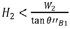


being the angle of the incident light with respect to a normal to the top surface of said diffraction grating and
- According to another embodiment of the disclosure, when said base pattern comprises one block of said dielectric material with refractive index n2 on top of said substrate, having a U shape, said U-shape consisting in two blocks of height H2 and width W2 separated by a central block of height H1, with H1 lower than H2, and
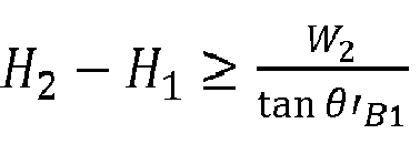

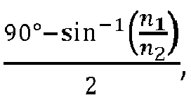
- According to another embodiment of the disclosure, W1 being said determined distance or a width of said central block, and W2 being the width of each of said two blocks or of each of said two lobes, W1 and W2 depend on a grating pitch d of said diffraction grating with


- According to another embodiment of the disclosure, said base pattern has a symmetric geometry. According to this embodiment, the optical device can be used in dual mode. For instance, it can be implemented in a waveguide which separates right hand side and left hand side of an input image to double the Field of View of the waveguide.
- According to another embodiment of the disclosure, said base pattern has an asymmetric geometry. According to this embodiment, the optical device is designd for single mode diffraction, for instance for in-coupler that just deviates the image into a signel side of a waveguide. This embodiment allows to have even bigger grating's pitch.
- According to another embodiment of the disclosure, said at least one diffraction grating is configured to diffract light for a group of wavelengths comprising more than one wavelength, and wherein said grating pitch is above the highest wavelength of said group of wavelengths.
- According to another embodiment of the disclosure, the optical device according to any one of the embodiments disclosed above comprises one diffraction grating per Red, Green and Blue color.
- According to another embodiment of the disclosure, the optical device is an optical waveguide. The optical device can advantageously be used as a waveguide, for instance a waveguide for AR/VR glasses.
- According to another embodiment of the disclosure, said at least one diffraction grating is configured for in-coupling light incoming into said optical waveguide or for extracting light out of said optical waveguide.
- According to another embodiment of the disclosure, said at least one diffraction grating is configured for in-coupling light incoming into said optical waveguide and wherein said optical waveguide comprises another diffraction grating configured for extracting light out of said optical waveguide, said other diffraction grating having a grating pitch above a wavelength of said light and said other diffraction grating being configured to diffract said light at a diffraction order having an absolute value equal to or greater than 2.
- According to another aspect of the present disclosure, an eyewear apparatus is disclosed. Such an eyewear apparatus comprises at least one optical device according to any one of the embodiments discsussed above.
- According to an embodiment of the disclosure, the eyewear apparatus comprises:
- a light display engine configured for emitting an image to display,
- a group of optics configured for coupling incoming light from the light display engine to said optical waveguide,
- said at least one optical waveguide being configured for guiding incoming light towards an eye of a user to make the image visible to the user.
- The present disclosure can be better understood with reference to the following description and drawings, given by way of example and not limiting the scope of protection, and in which:
-
Figure 1A illustrates the definition of theoretical critical and grazing rays in single mode, -
Figure 1B illustrates the definition of theoretical critical and grazing rays in dual mode, -
Figure 2 illustrates diffraction modes of an incident plane wave, -
Figure 3 illustrates the definition of important rays for the negative angular input space, -
Figures 4A and 4B illustrate an exemplary 60° field of view light engine. -
Figure 5 illustrate a schematic view of the Light engine fromfigures 4A and 4B with the waveguide provided with the in-coupling grating. -
Figure 6 illustrates an examplary Geometry and pitch size for a base pattern of the diffraction grating. -
Figure 7 illustrates diffraction performances of a grating structure illustrated withfigure 6 . -
Figure 8 illustrates diffraction performances of a grating structure illustrated withfigure 6 , but without the high index material. -
Figure 9 illustrates (a) a Cross-section view of a double-material metaelement with an insert as illustrated withfigure 6 ; (b) Power density distribution in the xy-plane for the metaelement with the parameters: n1 = 1.0, n2 = 2.105, W1 = 260nm, W2 =100nm,H=700nm,H2 =300nm. λ=625nm, θi =0°. -
Figure 10 illustrates (a) a Cross-section view of a double-material metaelement with an insert as illustrated withfigure 6 ; (b) Power density distribution in the xy-plane for the metaelement with the parameters: n1 = 1.0, n2 = 2.105, W1 = 260nm, W2 =100nm,H=700nm,H2 =300nm. λ=625nm,θi =30°. -
Figure 11 illustrates (a) Hy component distribution and (b) power density distribution in the xy-plane for the metaelement illustrated withfigure 6 with the parameters: n1 = 1.0, n2 = 2.105, n3 = 1.52, W1 = 260nm, W2 = 100nm, H = 700nm, H2 = 300nm. λ = 625nm. -
Figure 12 illustrates an exemplary geometry and pitch size for an alternative embodi ment of a base pattern of a diffraction grating. -
Figure 13 illustraes performance of a grating based on the geometry illustrated withfigure 12 . -
Figure 14A illustrates a cross-section view of a double-material metaelement with equal height insert (left part) and power density distributions in the xy-plane for the metaelement (right part) with the parameters: n1 = 1.0, n2 = 2.105, n3 = 1.52, W1 =260nm, W2 =130nm, H=305nm, H2 =300nm, λ=625nm and θi =0°. -
Figure 14B illustrates a cross-section view of a double-material metaelement with equal height insert (left part) and power density distributions in the xy-plane for the metaelement (right part) with the parameters: n1 = 1.0, n2 = 2.105, n3 = 1.52, W1 =260nm, W2 =130nm, H=305nm, H2 =300nm, λ=625nm and θi =30°. -
Figure 15 illutrates (a) Hy component distribution and (b) power density distribution in the xy-plane for the metaelement illustrated withfigure 12 with the parameters: n1 = 1.0, n2 = 2.105, n3 = 1.52, W1 = 260nm, W2 = 130nm, H = 305nm, H2 = 300nm, λ = 625nm. -
Figure 16 illustrates another exemplary geometry for a base pattern of a diffraction grating according to an embodiment of the present disclosure. -
Figure 17 illustrates performances of the structure illustrated withfigure 16 . -
Figure 18 illustrates an exemplary regular structure of a diffraction grating according to prior art. -
Figure 19 illustrates diffraction efficiencies for the structure illustrated withfigure 18 . -
Figure 20 illustrates cross-section views of a single-material metaelements illustrated withfigure 16 (left part) and withfigure 18 (right part) with the parameters: n1 = 1.0, n2 = 2.105, W1 =260nm, W2 =130nm,H=200nm, θi =0°. -
Figure 21 illustrates cross-section views of a single-material metaelements illustrated withfigure 16 (left part) and withfigure 18 (right part) with the parameters: n1 = 1.0, n2 = 2.105, W1 =260nm, W2 =130nm,H=200nm, θi =30°. -
Figure 22A illustrates (a) Hy component distribution and (b) power density distribution in the xy-plane for the single NJ element illustrated withfigure 18 with the parameters: n1 = 1.0,n2 = 2.105, n3 = 1.52, W1 = 260nm, W2 = 130nm, H2 = 200nm, λ = 625nm. -
Figure 22B illustrates (c) Hy component distribution and (d) power density distribution in the xy-plane for the twin structure metaelement illustrated withfigure 16 with the parameters: n1 = 1.0,n2 = 2.105, n3 = 1.52, W1 = 260nm, W2 = 130nm, H2 = 200nm, λ = 625nm. -
Figure 23 illustrates power density distribution in the xy-plane for the twin structure metaelement illustrated withfigure 16 with the parameters: n1 = 1.0, n2=2.105, W1 = 260nm, W2 = 130nm, H2 = 200nm, λ = 625nm; Left column - n3 = 2.105, right column - n3 = 1.52. -
Figure 24 illustrates another exemplary geometry for a base pattern of a diffraction grating according to an embodiment of the present disclosure. -
Figure 25 illustrates performance of the U shaped structure illustrated withfigure 24 . -
Figure 26 illustrates (a) Hy component distribution and (b) power density distribution in the xy-plane for the U-shaped metaelement illustrated withfigure 24 with the parameters: n1 = 1.0, n2 = 2.105, n3 = 1.52, W1 = 260nm, W2 = 130nm, H2 = 200nm, H1 = 50nm, λ = 625nm. -
Figure 27 illustrates tolerancing of the pitch size d = 823 ± 5nm. for the U shaped structure illustrated withfigure 24 : top part shows the performances for d = 818nm. -
Figure 28 illustrates an exemplary geometry and pitch size for another embodiment of the base pattern of the diffraction grating. -
Figure 29 illustrates performance of geometry illustrated withfigure 28 , the horizontal axis spans ±12 degrees. -
Figure 30 illustrates a perspective schematic view of an eyewear apparatus according to an embodiment of the present disclosure, -
Figure 31 illustrates a schematic front view of the eyewear apparatus illustrated withfigure 30 , -
Figure 32 illustrates an exemplary diffraction grating according to an embodiment of the present disclosure. - According to the present principle, an optical device comprising at least one diffraction grating will be described. According to embodiments of the present disclosure, such an optical device can be used as a waveguide for AR/VR glasses for instance.
- According to the present disclosure, the optical device presents a specific diffraction grating that can be used for in coupling light into the optical device and /or out coupling light from the optical device. According to the present principle, the diffraction grating is configured to diffract an incident light at a diffraction order having an absolute value equal to or greater than 2.
-
Figure 2 shows schematically what happens to a plane wave (PW) incident upon a linear grating (DG). The plane wave gets divided into diffraction modes (-2, -1, 0, +1, +2), which are angular spaced beams of local maximum intensity. In thefigure 2 , the diffracted modes number -2,-1,0, 1 and 2 are represented but higher orders exist. The order zero has in general the more power and is the natural mode into which the regular refraction or reflection would occur. We might also have diffracted modes in reflection. - In general, a grating generates a lot of diffraction orders. In numerous applications it is wishful to kill all other modes but the first one. An example of such gratings are thick holograms made by the interference of two plane waves.
- It is then the aim of the structure of the diffraction grating to privilege heavily on the first diffraction order and kill as much as possible of the remaining ones.
- All diffraction orders are linked to the incoming beam by the following mathematical formula:

- Usually, the light engine consists in light sources and one display. The light sources are power LED that are time sequentially driven and the design of the flat optics shall be adapted to the wavelengths of the LEDs. Example of common LEDs for near to eye projection are: Blue 459nm True Green 530nm Red 625nm The diffraction process is very dispersive. The diffraction angle is different for different wavelength as it varies linearly with the wavelength (MλT) which is quite a big variation. It is therefore necessary to find a mean to minimize chromatic aberrations. One way of handling this is to have one waveguide per color band as the diffraction grating needs to be different for each one. So if we are dealing with an RGB true color image, we would need to have three waveguides. This complicates their design.
-
Figure 3 shows the definition of some important rays used to characterize a waveguide. Capital superscript lettersand indicate respectively the grazing and critical rays. If the subscript is 1, the rays are outside of the waveguide, if it is 2, they are inside. In principle, the maximal input angular bandwidth of the grating from the figure is


figure 3 ) which correspond to the input angular range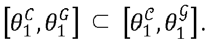


- The problem to solve now is to choose the grating's period d which can diffract the rays as illustrated in
figure 3 . We have to make some choices, particularly concerning the ray
- Let's say we need to extract the image approximately 4cm from the injection into the waveguide, this is the distance between the exit pupil of the light engine in the branches of glasses and the eye. Then we also suppose that the light engine and the eye are in the same half space with respect to the waveguide, this means that the extraction port is an even number. If we denote xi C,G the distance from an input of a critical ray or grazing ray before he bounce number i, i is called the extraction port. If i is even, the extraction port is on the same side than the light engine and if i is odd the extraction port is on the opposite side of the light engine. A way of using practically this definition of extraction port is to set a diffraction grating between the points [x2 C, x2 G] whose result would be to gather the image out of the waveguide by diffraction between those two points. The image is said to be extracted at
port number 2. - We also want a field of view of 24 degrees for a glass substrate of index 1.5. We can define in the next table, some values useful for the design of a system.
Table 1: Parameters for the design of the grating Inputs Calculated index n 2 1.52 Light engine field of View Δφ° 24 Waveguide's field of View Δθ° 30.14 critical ray angle inside of the waveguide 
43.80 grazing ray angle inside of the waveguide 
74.96 Length incoupling grating L (mm) 4.2 minimal thickness of glass plate for light engine's field of view (mm) 2.190 minimal thickness of glass plate for waveguide's field of view (mm) 2.404 Thickness of prototype t (mm) 2.4 Extraction port number k 6 Beginning of the extraction port 
13.810 End of the extraction port 
57.781 Extraction port length Lk (mm) 43.971 - In this typical system we see that a more reasonable value for the grazing angle in the waveguide could be chosen to be approx.


- In this way, we will be in the prior art condition discussed above which splits half of the field of view (i.e. half of the image) into one direction and the other half into another direction with the positive consequence to double the field of view. This means that


- But there is another important condition here. There should be no cross-talks between the positive and negative order, which means that for a given orientation hitting the in-coupler, there shall always be one and only one direction of diffraction and no energy into the other one. On
figure 3 , this condition will be met if


- The maximal angular span of the input beam for negative angles is


- Let us analyze the relationship between pitch size and wavelength from both equations Eq.1 and Eq. 4.
- For n2 ∈ [3/2, 2], and if we choose to work with second diffraction order, |M| = 2, then the structural relationship is d/λ ≥ 1 in any case, which means that we are in another dimension when compared to the wavelength. The structure will then be over- wavelength.
- If, instead of coupling the first diffraction order into the waveguide, we choose the grating's pitch so that we couple a higher order, the grating's pitch will be greater and we could avoid to be on the very limits of the micro fabrication processes.
- The table 2 shows the difference between a grating designed to couple second orders and a grating for first orders. The difference in pitch size is almost doubled. For the second diffraction orders, we get for the RGB in-couplers values of the pitch d625 = 822.4nm, d530 = 697.4nm, d460 = 605.3nm instead of the very small pitch sizes that are obtained for the first diffraction orders: d625 = 411.2nm, d530 = 348.7nm, d460 = 302.7nm.
- This is the reason those gratings (using second diffraction order) are called over-wavelength gratings as their pitch is always bigger than the wavelength of the color band they are designed for. On the other hand, the grating (using first diffraction order) can be called subwavelength gratings since their pitch is smaller than the wavelength of the color band they are designed for.
- The field of view from the table 2 is given for a system that uses both ±2 diffraction orders. It is twice the field of view of previous systems working in only one direction into the waveguide.
- In general there is a reason why people work with orders ±1! It is because it is possible to get a symmetric response curve into both directions for the very lower diffraction orders, while emphasizing either order +1 or order -1 with very high diffraction efficiency but also with enormous diffraction uniformity.
- As we will discuss below, the nanojet based diffraction gratings disclosed herein allows to get symmetric response into ±2 diffraction orders with also very high diffraction uniformity, which is a real strength.
Table 2: Grating's pitch and angular bandwith Index n 2 1.52 1.52 1.52 Diffraction order M 2 2 2 Wavelength λ (nm) 625 530 460 
-2.97 -2.97 -2.97 grazing ray angle inside of the waveguide 
75 75 75 Grating's period for 2nd order (nm) 822.4 697.4 605.3 Grating's period for 1st order (nm) 411.2 348.7 302.7 grazing incident angle for the real grazing ray in waveguide 

0.00 0.00 0.00 maximum input angle 
-31.33 -31.33 -31.33 FoV 56.73 56.73 56.73 -
Figures 4A and 4B illustrates an exemplary schematic light engine providing a 60° field of view. The light engine comprises a display emitting incoming light to a set of optics that couple incoming light to an exit pupil placed at the last surface after the last lens of the set of optics, where the rays intersect into the smallest circular cross section. - As will be seen in the
figure 5 , the diffraction grating is to be placed there. Onfigure 4A , we can see only rays of negative incident angle onto the in-coupling grating (exit pupil). Those rays come from the upper part of the display. Onfigure 4B , we can see only rays of positive incident angle onto the in-coupling grating (exit pupil). Those rays come from the lower part of the display. -
Figure 5 shows the light engine fromfigures 4A and 4B with the waveguide (WG) provided with the in-coupling grating. Order M = 2 is on the left hand side, order M = -2 on the right hand side. Both ray paths exist at the same time if the display is ON. There is a ±2.97° angular range along the center horizontal part of the display that does not contibute. This part of the display shall always be black. -
Figure 5 is a schematic view of the light engine obtained from simulation. Only incoupling of incoming light into the waveguide is shown. On the simulated view, light rays are not extracted at output using extraction ports. - In all following subsections, different geometries will be presented that achieve high performances for the new principle presented here.
- Different embodiments of geometry for a diffraction grating will be presented below, as well as the performances of such geometries. Also, a set of equations is presented to demonstrate the input from the edge diffraction phenomenon disclosed in " Near field focusing by edge diffraction", a. Boriskin, V. Drazic, R. keating, M. Damghanian, O. Shramkova, L. Blonde, Optics Letters, vol. 43, Issue 16, pp 4053-4056 (2018 ) in the single element of the period into the total response of the diffraction grating.
- The presented data were obtained using the COMSOL Multiphysics software. The presented analysis of the fields and power distributions inside the so-called metaelements of the gratings helps us to explain the physics of the phenomenon and to get optimal topologies. We assume that the system is illuminated by a linearly-polarized plane wave E = {0, 0, 1} (TE). The effect of the parameters of the single metaelement on the functionality of the system is considered. As it was demonstrated in the document cited above, the nanojet (NJ) beam-forming phenomenon is associated solely with the edge of the system. Based on the analysis of the wedge diffraction phenomenon as disclosed in Near field focusing by edge diffraction", a. Boriskin, V. Drazic, R. keating, M. Damghanian, O. Shramkova, L. Blondé, Optics Letters, vol. 43, Issue 16, pp 4053-4056 (2018 ), we can determine the deviation angle of nanojet (NJ) beam in the denser medium in the case of normal incidence of electromagnetic wave (θi = 90°).

- In the case of single wedge of single material element, the constructive interference phenomenon between jet wave generated by the wedge and plane waves refracted by the edges of this wedge leads to the creation of NJ beam.
- It shall be also noted that in the following, unless specified otherwise, n1 is the refractive index of host medium, n2 represents the refractive index of the high index material while n3 represents a lower refractive index, most of the time the glass substrate's index.
- An exemplary geometry for a base pattern of a diffraction grating configured to diffract light at a diffraction order having an absolute value equal to or greater than 2 is disclosed in
figure 6 . - In
figure 6 , the base pattern comprises two dieletric materials: a block ME2 of dielectric material with refractive index n2 placed on top of a layer ME3 of dieletric material with refractive index n3. The layer ME3 presents a block B3 of same dielectric material, the block B3 is inserted in block ME2. - The structure from
figure 6 has been optimized in order to deliver the best performances for the red wavelength at λ = 625nm. Other slightly varying parameters could be used for a variable aspect of the diffraction curves. This structure is symmetrical, as it needs to feed a positive and a negative diffraction order in a symmetric way. - In order to fabricate the structure, a glass etching is first needed to generate the first structure (layer ME3) into the waveguide's base material. Then an ebeam lithography resist in spin coated on top of the structure and again exposed and etched to add the second component (ME2 block).
- Both ME2 and ME3 components are dielectric transparent materials. This structure, as can be seen from the dimensions ilustrated on
figure 6 , has a much bigger pitch than in the prior art: 822.4nm instead of 496nm. The aspect ratio is of 700/460 ≈ 1.5 which is a low one, the depth is not much bigger than the width. -
Figure 7 illustrates the diffraction performances of the grating illustrated onfigure 6 . WE can see fromfigure 7 that nmax ≈ 65%,
Order 0,+1 and -1 do not couple into the waveguide, they transmit through and will not reduce the virtual image contrast. - Considering
figure 7 , we can see from the analysis that the diffraction uniformity is of the same order than the prior art systems, but we use here second order diffraction while the prior art systems use first order. We have not kept in this system the very high uniformity we were able to achieve with nanojet enhanced diffraction grating of lower order, but we were able to get a very high diffraction efficiency like it is emphasized infigure 8 (discussed below) where we plot the diffraction efficiency of the same system but without nanojet enhancement (we removed the high index material to keep only the etched waveguide). -
Figure 8 illustrates the diffraction performances of the grating structure offigure 6 but without the high index material (ME2). As can be seen onfigure 8 , the diffraction efficiency of +2 and -2 orders in that case are marginal. - We discuss now the nanojet analysis of the energy transfer to higher orders
Figure 9 illustrates (a) a cross-section view of a double-material metaelement with the insert as illustrated infigure 6 for instance, and (b) the power density distribution in the xy-plane for such a metaelement with the parameters: n1 = 1.0, n2 = 2.105, W1 = 260nm, W2 =100nm, H=700nm,H2 =300nm. λ=625nm, θi =0°. - Let us consider the symmetrical metaelement combining the dielectric block with refractive index n3, width W1 and height H2 inside the dielectric block with the refractive index n2, width 2W2 + W1 and total height H (as illustrated in
figure 9 ). We assume that n1 is the refractive index of host medium and n1 < n2 < n3. As a result, in the proposed system for θi = 0° (θi is the angle of incidence) we will observe radiation of 4 nanojets with deviation angle
- For the proposed symmetrical system two opposite edges of the big block (ME3 in the
Figure 9 will generate 2 nanojets propagating inside the block ME3 with refractive index n2 with radiation angles θ B1 (NJ1, see dashed lines starting at top edges of block ME2 inFigure 9 ). As we can see, the hot spot of power distribution inside the metaelement inFig. 9(b) corresponds to the crossing point of these two NJs. It is necessary to mention that in this cross-section view we did not take into account the refraction phenomenon at the boundaries between the insert B3 and main block ME2. - Second couple of NJs with radiation angles θ B2 inside the big block ME2 with refractive index n2 is generated by the edges of the central block B3 with refractive index n3 (NJ2, see dashed lines starting at top edges of block B3 in
Fig. 9(a) ). The propagation direction of these NJs will be changed due to the total internal reflection of the waves at the vertical edges of the big block ME2. As a result, at the bottom surface of the metaelement, we can observe 2 less intensive hot spots in the crossing points of NJ1 and NJ2 (crossing points of the dashed lines NJ1 and NJ2 on each side of block B3). -
Figure 10 illustrates (a) the cross-section view of a double-material metaelement with the insert, for instance as the one illustrated infigure 6 , and (b) the power density dis tribution in the xy-plane for the metaelement with the parameters: n1 = 1.0, n2 = 2.105, W1 = 260nm, W2 =100nm,H=700nm,H2 =300nm. λ=625nm,θi =30°. - To explain the redistribution of the intensity inside the metaelements in the case of plane wave oblique incidence, we should take into account that the radiation angles θ' and θ" for opposite edges of the system are not equal (see
Fig. 10(a) ). As a result, for the main part we can have:
- In a similar way, the nanojets beam radiation angles for the insert (block B3) can be determined as:

- The reflection of the generated waves at the edges of the constitutive parts of the metaelements leads to the creation of the new NJ hot spots (cross points) and nonsymmetrical redistribution of the total power inside the metalements, as can be seen with
figure 10(b) . - Let us put these elements onto the substrate with refractive index n3 on
Figure 6 .Figure 11 (a) illustrates the Hy component field distribution (i.e. the distribution corresponding to the projection of the magnetic field on the y axis) andfigure 11 (b) shows the power density distribution in the xy-plane for the metaelement as illustrated infigure 6 , with the parameters: n1 = 1.0, n2 = 2.105, n3 = 1.52, W1 = 260nm, W2 = 100nm, H = 700nm, H2 = 300nm. λ = 625nm, for the 3 different angles of incidence θi. - Here, below the metaelement, we can observe the NJs inside the substrate (ME3) after the corresponding wave refraction at the substrate surface. The power distribution presented in
Figure 11(b) shows the intensive lobes inside the substrate generated in the result of wave interference. The constructive interference between the refracted waves obtained as a result of wedge diffraction of the periodic array of metaelements leads to the redistribution of the power between corresponding orders of diffraction. We should note that the central insert (B3) with lower refractive index helps us to almost fully suppress the intensity of 0-diffraction order in a case of normal incidence and to dramatically decrease it in the case of inclined incidence. Finally, we observe that the presented topology helps us to change the direction of propagation of the waves diffracted by the wedges of the elements of diffraction grating and to increase the intensity of ±2nd diffraction orders (seeFig.7 ). - The structure from
figure 6 is not the only one that could be used in order to achieve right performances, even if it might be a preferred one for the micro-fabrication process. Another geometry for the base pattern according to another embodiment, is depicted onfigure 12 . Such a geometry can achieve comparable performances - In the embodiment illustrated in
figure 12 , the base pattern comprises a block B3 of same dielectric material with refractive index n3 as the substrate ME3. The block B3 is placed on top of the substrate ME3 and between two blocks ME21 and ME22 of dielectric material with refractive index n2. The blocks B3, ME21 and ME22 have an identical height. - Numerical values indicated in
figure 12 have been optimized for a wavelength of 625nm. However, slightly different values may be used for the wavelength of 625nm. Also, other numerical values could be used for other wavelength, as long as the grating pitch d is above the wavelength of the ligth it is dedicated to diffract. -
Figure 13 illustrates performances of a diffraction grating based on the geometry fromfigure 12 . - As can be seen from
figure 13 , The maximum diffraction efficiency is of 55 percent which is low but if we can use a material n2 with higher values (2.3 to 2.5) the efficiency will increase significantly. The value used of n2 = 2.105 is based on available silicon nitride ebeam lithography compatible material. Now, we discuss the nanojet analysis of the energy transfer to higher orders. We consider the symmetrical metaelement combining the block with refractive index n3, width W1 and height H placed between 2 similar blocks with the refractive index n2, width W2 and total height H, as illustrated withfigure 12 . We assume that n1 is the refractive index of host medium and n1 < n2 < n3. -
Figure 14A illustrates the cross-section views of a double-material metaelement with equal height insert (left part offigure 14A ) and power density distributions in the xy-plane (right part offigure 14A ) for the metaelement with the parameters: n1 = 1.0, n2 = 2.105, n3 = 1.52, W1 =260nm,W2 =130nm,H=305nm,H2 =300nm. λ=625nm and θi =0°. Figrue 14B illustrates the same but with θi =30°. As a result, in a case of normal incidence (Figure 14A ) we will observe 2 NJs generated by the external edges between the media with refractive index n2 and host medium and propagating at the angles θB1 and 2 NJs generated at the edges between the blocks with refractive index n2 and n3 and propagating at the angles θB2 (see dashed lines infigure 14A ). - As we can see, two hot spots of power distribution inside the similar blocks with refractive index n2 in
figure 14A corresponds to the crossing point of two NJs with different radiation angles. The transmission of jet waves diffracted by the external wedges into the central part (insert) of the element leads to the creation of a new hot spot outside the structure along the axis of the symmetry of the metaelement. - It is necessary to note that representing the schematic distribution of the NJs we did not take into account the refraction phenomenon leading to the shift of the NJs' crossing point along the axis of the symmetry. The existence of such NJ hot spot for each metaelement explains the high intensity of 0-diffraction order in a case of normal incidence (see
Fig.13 ). -
Figure 15 illustrates the Hy component field distribution (a) and power density distribution (b) in the xy-plane for a metaelement as illustrated infigure 12 , with the parameters: n1 = 1.0, n2 = 2.105, n3 = 1.52, W1 = 260nm, W2 = 130nm, H = 305nm, H2 = 300nm. λ = 625nm, for 3 different angle of incidence, when the geometry structure illustrated infigure 12 is placed with a substrate of dielectric material having refractive index n3. - Changing the angle of electromagnetic wave incidence from 0 to +30 degrees, we observe that the waves diffracted by the internal wedges (wedges of the inserts) transmit into the substrate (see
Fig. 15(a) ) and make an input into the 2nd diffraction order. The power distribution presented inFig. 15(b) shows the intensive lobes inside the substrate generated in the result of diffrated waves' interference. For the negative angles of incidence, we observe the intensification of ±2nd diffraction order. As in the case of the metaelements with the inserts (figure 6 ), the total internal reflection phenomenon plays a crucial role by changing the propagation direction of diffracted waves and leading to the redistribution of the power between corresponding diffraction orders. -
Figure 16 illustrates a base pattern according to another embodiment of the present principle. The base pattern of the structure is based here on a high index single material having a refractive index n2 deposited and e-beamed on a glass substrate ME3 having a refractive index n3. According to the present embodiment, this results in two blocks ME21 and ME22 of single material having refractive index n2 and having same dimensions placed on top of the substrate ME3 and separated by a determined distance W1. The space separating the two blocks ME21 and ME22 is naturally filled with the host medium (with refractive index n1). - For this geometry, there is no glass etching required, and no multiple e-beam lithography, and these two facts are great advantages for the micro-fabrication. The structures are also very shallow with a height H2 of 200nm in the example presented here, to compare with the embodiment illustrated in
figure 6 which has a height of 700nm. -
Figure 17 illustrates the performance of the twin structure offigure 16 . Onfigure 17 , we can see that ηmax = 75%, ┌ = 64% from 3 to 30 and -30 to -3 degrees. - The performances are very good since we achieve a maximum diffraction efficiency of 75% and a diffraction uniformity of 64%. Those values are excellent and real improvements when compared to structures from
figures 6 and12 . - It is interesting also to see what happens to performances for a regular grating which is not optimized, neither nanojet wise nor for the second diffraction order, according to prior art systems. Such a geometry is illustrated in
figure 18 showing a single material of refractive index n2 deposited on a glass substrate with refractive index n3.Figure 19 shows the very poor diffraction efficiency of second orders in that case. - We now discuss the nanojet analysis of the energy transfer to higher orders for the twin structure illustrated on
figure 16 . -
Figure 20 illustrates the cross-section views of single-material metaelements for the embodiment illustrated infigure 16 (figure 20 (a) ) and for a single material metaelement as a single block (B1,figure 20 (b) ), with the parameters: n1 = 1.0, n2 = 2.105, W1 =260nm, W2 =130nm, H=200nm, θi =0°.Figure 21 illustrates the same asfigure 20 but with an incident angle of the electromagnetic wave θi =30°. -
Figure 22A illustrates the Hy component field distribution (a) and power density distribution (b) in the xy-plane for the single NJ element B1 of right part offigure 20 for three different incident angles andfigure 22B illustrates the Hy component field distribution (c) and power density distribution (d) in the xy-plane for the twin structure metaelements ME21 and ME22 of left part offigure 20 . In both cases, the parameters are the following: n1 = 1.0, n2 = 2.105, n3 = 1.52, W1 = 260nm, W2 = 130nm, H2 = 200nm, λ = 625nm. - The total internal reflection phenomenon helps us to modify the response of the system in the case of single material elements. Let us consider the 2 similar dielectric blocks ME22 and ME21 with refractive index n2, width W2 and height H2. In
figure 20(a), and 21(a) , we assume that W1 is the distance between the elements and n1 is the refractive index of host medium and n1 < n2 < n3. - Let us compare this twin system with the single dielectric block B1 with refractive index n2, width W1 + 2W2 and height H2 illustrated in
figure 20(b) and 21(b) . In the single NJ element system, we have just 2 NJs associated with 2 external edges (left and right edges) of the block B1 (seeFigure 20(b) , dashed lines correspond to NJ beams with the deviation angle θB1). - The existence of two additional edges in the double block system or twin structure for θi = 0 degrees leads to radiation of 4 NJs (2 NJs in each block for left and right edges) with deviation angles θB1 (see dashed lines in
Figure 20 , dashed lines indicated by IJW correspond to the NJ beams generated by the internal edges in the twin system (Figure 20(a) ). By changing the distance between the internal edges, we can satisfy the condition of constructive and destructive interference for the corresponding waves diffracted by the right or left edges of the elements and propagating in the same direction. Finally, for the parameters of the system mentioned above, we get that diffracted waves propagating in the same direction will interfere destructively or constructively. So, we can intensify or suppress the distributions at corresponding angles (seeFigure 22B(c) ). - For a case of normal incidence, the radiation angles of all NJs are the same θB1. Comparing the power distribution for these systems, we can conclude that in a case of twin structure the existence of two additional internal edges leads to the decrease of the intensity of the central NJ (this central NJ resulting from the intersection of NJs generated by the external edges of the element is directed along the axis of the symmetry of metaelements) and to the beginnings of 2 additional NJs with higher intensity resulting from the intersection of NJs generated by the external and internal edges of the blocks.
- For the inclined incidence, we get first pair of NJs with radiation angles


- The combination of constructive and destructive phenomena for each pair with the total internal reflection of the waves for some angles of incidence leads again to the redistribution of the intensity between the corresponding diffraction orders for the periodic array of the metaelements. As a result, we can suppress ±1st diffraction orders and dramatically increase the intensities of ±2nd diffraction orders as illustrated by the comparison of
Figures 17 and19 . - To optimize the response of this system we should consider some parameters' restrictions to provide intensification of ±2nd diffraction orders for the proposed topology. To get maximal intensity of the 2nd diffraction order, in the case of negative angles of incidence we must take the twin elements with such parameters:
- 1. To change the direction of NJs generated by the left vertical edge of the elements, we must take

- 2. To avoid the reflection of the NJs generated by the right vertical edges of the elements, we should take

- 3. The width of corresponding blocks and distance between the blocks depend on the period of diffraction grating:


- 4. It is necessary to note that inside each block the NJs generated by the opposite edges will intersect at some point A (see
Fig.21 ). The distance between the top of each block and this point of intersection can be determined as

- In a case of positive angles of incidence, taking the twin elements with such parameters, we observe an intensified +2nd diffraction order.
- Considering a diffraction grating presenting a periodic array of the twin metaelements placed on the substrate with lower refractive index as illustrated in
figure 16 , we should remember about refraction of the wave diffracted by the edges of the metaelements at the boundary between the substrate and elements affecting the angle NJ deviation.Figure 23 illustrates the power density distribution in the xy-plane for the twin structure metaelement with the parameters: n1 = 1.0, n2=2.105, W1 = 260nm, W2 = 130nm, H2 = 200nm, λ = 625nm; and n3 = 2.105 for the left column and n3 = 1.52 for the right column. -
Figure 24 illustrates another embodiment for a base pattern of a diffaction grating of an optical device according to the present principle. According to this embodiment, the base pattern consists in a block ME2 of single material having a refractive index n2 and having a U shape, placed on top of a substrate ME3 having refractive index n3. Values presented onfigure 24 are only examples. More precisely, the U-shape form is commonly known as a form forming the letter U. Onfigure 24 , it can be seen, that the block ME2 has two lobes or blocks of single material having a refractive index n2 of height H2 and width W2 separated by a band of same single material having a refractive index n2 of height H1 and width W1. - Geometry wise, a high index n2 single material is deposited and e-beamed on a glass substrate ME3. There is no glass etching required, and no multiple e- beam lithography, and these two facts are great advantages for the micro-fabrication.
- The structures are also very shallow with a height of 200nm, to compare with the embodiment disclosed with
figure 6 which has a height of 700nm. - As illustrated by
figure 25 , the performances are very good since we achieve a maximum diffraction efficiency of 65%, which is somewhat lower than the efficiency achieved with the twin structure, but here, it is the diffraction uniformity which reaches excellence with a value of ┌ = 87%. Those values are excellent and real improvements when compared to structures fromfigures 6 and12 . -
Figure 26 illustrates the Hy component distribution (top part) and power density distribution (bottom part) in the xy-plane for the U-shaped metaelement illustrated infigure 24 , with the parameters: n1 = 1.0, n2 = 2.105, n3 = 1.52, W1 = 260nm, W2 = 130nm, H2 = 200nm, H1 = 50nm, λ = 625nm. - Let us note that the U-shape metaelement with higher refractive index n2 helps to decrease the intensity of central NJ in a case of normal incidence and increase the intensity of the side lobes.
- Finally, we observe that for the U-shaped topology we can increase the intensity of ±2nd diffraction orders for the small angles of incidence and improve the diffraction uniformity as illustrated by the performances shown on figure (see
Figure 25 ). - To determine the height of the central block (H1) we should take into account that for some particular angles of incidence the NJs generated by the left edge of the left block (in the case of negative angles of incidence) or by the right edge of the right block (in the case of positive angles of incidence) will not be reflected by the opposite edges and will not change the direction of propagation. For the rest of the incidence angles we must take

- Equations for

- The width W1 of the central band separating the two lobes of the U-shape should also satisfy the relations defined for W1 and W2 in the twin structure.
- The values provided for the U-shaped structure must be tolerance robust, and the pitch variation has been investigated in order to check the precision required for the fabrication. The original pitch is d = 823nm.
-
Figure 27 illustrates the tolerancing in the pitch size for d = 818nm and d = 832nm. The top part offigure 27 represents the performances for d = 818nm. It has ηmax = 65%, ┌ = 81.8%. The bottom part offigure 27 represents the performances for a pitch of d = 832nm. It is of ηmax = 78.5%, ┌ = 76.2%. If the performances are good for 832nm, they will be good for 828nm too. - From
figure 27 , we can see that diffraction orders ±2 still have a high diffraction efficiency and uniformity for d = 823±5nm. - We have previously described over-wavelength structure for dual mode diffraction. Such dual mode diffraction was achieved thanks to the symetric structure of the base pattern of the diffraction grating.
- The principle discussed above (having over-wavelength grating pitch and second order diffraction) can also be extended to an in-coupler that just deviates the image into a single side of the waveguide instead of deviating positive angles into one direction and negative angles into another one.
- For that purpose, the geometry needs to break the symmetry in order to enhance one diffraction order.
Figure 28 illustrates a geometry and pitch size for an alternative embodiment of the base pattern of the diffraction grating. We can see onfigure 28 , that the grating's pitch is even bigger (988 nm in that case), it is almost a micro-meter sized spacing, its aspect ratio is close to 1. - According to such an embodiment, the base pattern is similar to the geometry illustrated with
figure 6 , but with a height on the right side that is lower than the height on the left side, to break the symetry. -
Figure 29 illustrates the performance of such a geometry. The horizontal axis spans ±12 degrees. We can see that the curve is the +2 diffraction order efficiency as a function of the angle of incidence. This structure achieves a maximum efficiency of 84 percent and a uniformity of 54 percent for input angles spanning ±12 degrees. -
Figure 32 illustrates an exemplary diffraction grating according to an embodiment of the present disclosure. Accoding to the embodiment, the base pattern of the diffraction grating has a U-shape as illustrated withfigure 24 . - According to an embodiment of the present disclosure, the diffraction grating having a base pattern according to any one of the embodiments disclosed herein can be dedicated to diffract only a given wavelegth. For instance, when used in a optical waveguide, one diffraction grating per RGB color can be used. This embodiment allows to minimize chromatic aberrations and a grating dedicated to a narrow band has a much better performance in terms of FoV.
- According to another embodiment of the present disclosure, the diffraction grating is configured to diffract light for a group of wavelengths comprising more than one wavelength. In that case, the NJ structure base pattern of the diffraction grating should be configured such that the grating pitch is above the highest wavelength of the group of wavelengths. For example,


- According to an embodiment of the present disclosure, the diffraction grating having a base pattern according to any one of the embodiments disclosed herein can be used in an optical waveguide, for instance for use in a waveguide in AR/VR glasses.
- According to this embodiment, the diffraction grating can be configured for in-coupling light incoming into the optical waveguide or for extracting light out of the optical waveguide depending on where the diffraction grating is formed on the waveguide.
- According to another embodiment of the present disclosure, the optical waveguide can comprise two diffraction gratings according to any one of the embodiments disclosed herein: one diffraction grating configured for in-coupling light incoming into said optical waveguide and another diffraction grating configured for extracting light out of said optical waveguide.
- Each diffraction grating having a grating pitch above a wavelength of the light it is configured to in couple or out couple, and both diffraction grating being configured to diffract said light at a diffraction order having an absolute value equal to or greater than 2.
- According to an embodiment of the present disclosure, an eyeware apparatus is disclosed which comprises an optical device accoding to any one of the embodiment disclosed above.
-
Figure 30 illustrates a perspective schematic view of an eyewear apparatus according to an embodiment of the present disclosure, andfigure 31 illustrates a schematic front view of the eyewear apparatus illustrated withfigure 30 . - According to an embodiment of the present disclosure, such an eyeware apparatus comprises:
- a light display engine (not shown) configured for emitting an image to display, the light engine display could for instance be placed on the branches of the eaywear apparatus,
- a group of optics (OPTICS) configured for coupling incoming light from the light display engine to the optical waveguide (WG).
- According to the embodiment disclosed here, the optical waveguide (WG) is configured for guiding incoming light towards an eye of a user to make the image visible to the user.
- According to the embodiment illustrated on
figure 30 , optical waveguide (WG), also referenced with a "1" comprises an input grating ("2"onfigure 30 ) playing the role of an in-coupler. The input grating may be a diffraction grating according to any of the embodiments described above. - The optical waveguide also comprises a vertical eye-pupil expander ("3" on
figure 30 ), a horizontal eye-pupil expander ("4" onfigure 30 ) and an output grating ("5" onfigure 30 ) or out-coupler. According to an embodiment of the present disclosure, the output grating may be a diffraction grating according to any of the embodiments described above. - As shown on
figure 31 , in order to have a stereoscopic view, image is emitted from two light engines (not shown) placed respectively on the two branches of the eyewear apparatus. The eyewear apparatus also comprising two waveguides (WG) on each side of the apparatus, as well as two sets of optics (OPTICS) for guiding the light from the respective light engine to the respective waveguide.
Claims (15)
- An optical device comprising at least one diffraction grating, wherein said at least one diffraction grating is configured to diffract a light of at least one given wavelength incident on said optical device, wherein said at least one diffraction grating has a grating pitch above said at least one given wavelength, wherein said at least one diffraction grating is configured to diffract said incident light at a diffraction order having an absolute value equal to or greater than 2, wherein the optical device is an optical waveguide configured for guiding said light diffracted at a diffraction order having an absolute value equal to or greater than 2.
- The optical device according to claim 1, wherein said at least one diffraction grating comprises a base pattern comprising at least one dielectric material, said base pattern being configured to form a nanojet beam associated with edges of the base pattern from said light incident on said at least one diffraction grating.
- The optical device according to any one of claims 1-2, wherein said at least one diffraction grating comprises at least one dielectric material with refractive index n2 deposited on a substrate with refractive index n3, and n3 < n2.
- The optical device according to claim 3, wherein said base pattern of said at least one diffraction grating is configured according to at least any one of the following arrangements:- said base pattern comprises a block of a same dielectric material with refractive index n3 as said substrate, on top of said substrate, said block of a same dielectric material with refractive index n3 being inserted into one block of said dielectric material with refractive index n2, or,- said base pattern comprises a block of same dielectric material with refractive index n3 as said substrate, on top of said substrate, said block of a same dielectric material with refractive index n3 being placed between two blocks of dielectric material with refractive index n2, said block of dielectric material with refractive index n3 and said two blocks of dielectric material with refractive index n2 having identical height, or- said base pattern comprises two blocks of dielectric material with refractive index n2 having identical dimensions, on top of said substrate, said two blocks being placed at a determined distance, or,- said base pattern comprises one block of said dielectric material with refractive index n2 on top of said substrate, said block having a U shape.
- The optical device according to claim 4, wherein when said base pattern comprises two blocks of dielectric material with refractive index n2 having identical dimensions, on top of said substrate, said two blocks being placed at a determined distance W1, said two blocks have a height H2 with


- The optical device according to claim 4, wherein when said base pattern comprises one block of said dielectric material with refractive index n2 on top of said substrate, having a U shape, said U-shape consisting in two lobes of height H2 and width W2 separated by a central block of height H1, with H1 lower than H2, and


- The optical device according to any one of claims 5 or 6, with W1 being said determined distance or a width of said central block, and W2 being the width of each of said two blocks or of each of said two lobes, W1 and W2 depend on a grating pitch d of said diffraction grating with
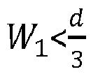

- The optical device according to any one of claims 1-7, wherein said base pattern has a symmetric geometry.
- The optical device according to any one of claims 1-7, wherein said base pattern has an asymmetric geometry.
- The optical device according to any one of claims 1-9, said at least one diffraction grating is configured to diffract light for a group of wavelengths comprising more than one wavelength, and wherein said grating pitch is above the highest wavelength of said group of wavelengths.
- The optical device according to any one of claims 1-10, comprising one diffraction grating per Red, Green and Blue color.
- The optical device according to any one of claims 1-10, wherein said at least one diffraction grating is configured for in-coupling light incoming into said optical waveguide or for extracting light out of said optical waveguide.
- The optical device according to any one of claims 1-10, wherein said at least one diffraction grating is configured for in-coupling light incoming into said optical waveguide and wherein said optical waveguide comprises another diffraction grating configured for extracting light out of said optical waveguide, said other diffraction grating having a grating pitch above a wavelength of said light and said other diffraction grating being configured to diffract said light at a diffraction order having an absolute value equal to or greater than 2.
- An eyewear apparatus, comprising at least one optical device according to any one of claims to any one of claims 1-13.
- An eyewear apparatus according to claim 14, comprising:- a light display engine configured for emitting an image to display,- a group of optics configured for coupling incoming light from the light display engine to said optical waveguide,- said at least one optical waveguide being configured for guiding incoming light towards an eye of a user to make the image visible to the user.
Priority Applications (5)
| Application Number | Priority Date | Filing Date | Title |
|---|---|---|---|
| EP18215212.4A EP3671293A1 (en) | 2018-12-21 | 2018-12-21 | An optical device comprising at least one diffraction grating having a grating pitch above the wavelength |
| US17/416,381 US12228756B2 (en) | 2018-12-21 | 2019-12-20 | Optical device |
| CN201980091736.5A CN113544551B (en) | 2018-12-21 | 2019-12-20 | Optical equipment |
| EP19831742.2A EP3899606A1 (en) | 2018-12-21 | 2019-12-20 | Optical device |
| PCT/EP2019/086776 WO2020128030A1 (en) | 2018-12-21 | 2019-12-20 | Optical device |
Applications Claiming Priority (1)
| Application Number | Priority Date | Filing Date | Title |
|---|---|---|---|
| EP18215212.4A EP3671293A1 (en) | 2018-12-21 | 2018-12-21 | An optical device comprising at least one diffraction grating having a grating pitch above the wavelength |
Publications (1)
| Publication Number | Publication Date |
|---|---|
| EP3671293A1 true EP3671293A1 (en) | 2020-06-24 |
Family
ID=64899223
Family Applications (2)
| Application Number | Title | Priority Date | Filing Date |
|---|---|---|---|
| EP18215212.4A Withdrawn EP3671293A1 (en) | 2018-12-21 | 2018-12-21 | An optical device comprising at least one diffraction grating having a grating pitch above the wavelength |
| EP19831742.2A Pending EP3899606A1 (en) | 2018-12-21 | 2019-12-20 | Optical device |
Family Applications After (1)
| Application Number | Title | Priority Date | Filing Date |
|---|---|---|---|
| EP19831742.2A Pending EP3899606A1 (en) | 2018-12-21 | 2019-12-20 | Optical device |
Country Status (4)
| Country | Link |
|---|---|
| US (1) | US12228756B2 (en) |
| EP (2) | EP3671293A1 (en) |
| CN (1) | CN113544551B (en) |
| WO (1) | WO2020128030A1 (en) |
Cited By (13)
| Publication number | Priority date | Publication date | Assignee | Title |
|---|---|---|---|---|
| WO2021053182A1 (en) | 2019-09-19 | 2021-03-25 | Interdigital Ce Patent Holdings | Optical device for coupling a high field of view of incident light |
| WO2022008378A1 (en) * | 2020-07-06 | 2022-01-13 | Interdigital Ce Patent Holdings, Sas | Reflective in-coupler design with high refractive index element using second diffraction order for near-eye displays |
| WO2022034060A1 (en) * | 2020-08-13 | 2022-02-17 | Interdigital Ce Patent Holdings, Sas | Low distortion imaging through a c-shape flat optical architecture |
| WO2022157228A1 (en) * | 2021-01-21 | 2022-07-28 | Interdigital Ce Patent Holdings, Sas | Uniform incoupler for conical incidence |
| US11573356B2 (en) | 2018-03-13 | 2023-02-07 | Interdigital Ce Patent Holdings | Diffraction grating comprising double-materials structures |
| US11604363B2 (en) | 2018-03-13 | 2023-03-14 | Interdigital Ce Patent Holdings | Image sensor comprising a color splitter with two different refractive indexes |
| US11972508B2 (en) | 2018-07-02 | 2024-04-30 | Interdigital Ce Patent Holdings, Sas | Image sensor comprising a color splitter with two different refractive indexes, and different height |
| US12174512B2 (en) | 2018-12-18 | 2024-12-24 | Interdigital Ce Patent Holdings | Device for forming an outgoing electromagnetic wave from an incident electromagnetic wave |
| US12210155B2 (en) | 2018-06-29 | 2025-01-28 | Interdigital Ce Patent Holdings | Optical device comprising a multi-layers waveguides |
| US12214493B2 (en) | 2018-12-18 | 2025-02-04 | Interdigital Ce Patent Holdings, Sas | Optical manipulation apparatus |
| US12228756B2 (en) | 2018-12-21 | 2025-02-18 | Interdigital Ce Patent Holdings, Sas | Optical device |
| US12306405B2 (en) | 2020-04-06 | 2025-05-20 | Interdigital Ce Patent Holdings, Sas | Waveguide display with cross-polarized eye pupil expanders |
| US12326562B2 (en) | 2020-03-23 | 2025-06-10 | Interdigital Ce Patent Holdings, Sas | Waveguide display system with wide field of view |
Families Citing this family (2)
| Publication number | Priority date | Publication date | Assignee | Title |
|---|---|---|---|---|
| CN116338856B (en) | 2023-04-19 | 2023-09-29 | 嘉兴驭光光电科技有限公司 | Optical waveguide device for display and display apparatus having the same |
| JP7583218B1 (en) | 2024-06-28 | 2024-11-13 | 日本センヂミア株式会社 | Rolling mill |
Citations (6)
| Publication number | Priority date | Publication date | Assignee | Title |
|---|---|---|---|---|
| WO2009083977A2 (en) * | 2008-01-02 | 2009-07-09 | Mirage Innovations Ltd. | Optical device for relaying polychromatic light |
| US20090190094A1 (en) * | 2006-09-28 | 2009-07-30 | Brother Kogyo Kabushiki Kaisha | Optical system for light flux transfer, and retinal scanning display using such an optical system |
| US20160231568A1 (en) | 2015-02-09 | 2016-08-11 | Microsoft Technology Licensing, Llc | Waveguide |
| WO2017180403A1 (en) | 2016-04-13 | 2017-10-19 | Microsoft Technology Licensing, Llc | Waveguides with extended field of view |
| EP3339938A1 (en) * | 2015-08-20 | 2018-06-27 | Hoya Lens Thailand Ltd. | Optical device |
| US20180231771A1 (en) * | 2017-02-15 | 2018-08-16 | Magic Leap, Inc. | Projector architecture incorporating artifact mitigation |
Family Cites Families (114)
| Publication number | Priority date | Publication date | Assignee | Title |
|---|---|---|---|---|
| US3718383A (en) | 1971-04-19 | 1973-02-27 | Eastman Kodak Co | Plastic optical element having refractive index gradient |
| JP3891628B2 (en) * | 1997-02-04 | 2007-03-14 | オリンパス株式会社 | Illumination optical system and endoscope system including the same |
| EP1118884A4 (en) | 1999-08-04 | 2005-04-06 | Nippon Sheet Glass Co Ltd | Echelon diffraction grating and optical waveguide element |
| JP4345256B2 (en) | 2001-02-14 | 2009-10-14 | 旭硝子株式会社 | Wavelength selective diffraction element and optical head device |
| JP4049553B2 (en) | 2001-06-25 | 2008-02-20 | 日本放送協会 | Stereoscopic image transmitting apparatus and stereoscopic image receiving apparatus |
| CN1526079A (en) | 2001-07-10 | 2004-09-01 | 住友电气工业株式会社 | Optical waveguide type diffraction grating element and manufacturing method thereof |
| WO2003025635A1 (en) | 2001-09-19 | 2003-03-27 | Technion Research & Development Foundation Ltd. | Space-variant subwavelength dielectric grating and applications thereof |
| AU2003257697A1 (en) | 2002-09-19 | 2004-04-08 | Sumitomo Electric Industries, Ltd. | Diffractive optical device and method for producing same |
| CN101241202A (en) | 2003-01-24 | 2008-08-13 | 住友电气工业株式会社 | Diffraction grating element |
| JP4609318B2 (en) | 2003-02-18 | 2011-01-12 | 住友電気工業株式会社 | Diffraction grating element |
| TWI319124B (en) | 2003-02-27 | 2010-01-01 | Asml Netherlands Bv | Stationary and dynamic radial transverse electric polarizer for high numerical aperture systems |
| CN100386653C (en) | 2003-03-13 | 2008-05-07 | 旭硝子株式会社 | Diffractive elements and optical devices |
| KR101162135B1 (en) | 2003-03-13 | 2012-07-03 | 아사히 가라스 가부시키가이샤 | Diffraction element and optical device |
| US20040198582A1 (en) | 2003-04-01 | 2004-10-07 | Borrelli Nicholas F. | Optical elements and methods of making optical elements |
| US20060250933A1 (en) | 2003-04-25 | 2006-11-09 | Asada Jun-Ichi | Optical diffraction device and optical information processing device |
| FI115169B (en) * | 2003-05-13 | 2005-03-15 | Nokia Corp | Method and optical system for coupling light to a waveguide |
| JP5055694B2 (en) | 2003-12-26 | 2012-10-24 | 旭硝子株式会社 | Polarizing diffraction element and optical head device |
| CN101614837A (en) | 2003-12-26 | 2009-12-30 | 旭硝子株式会社 | Polarization diffraction element and optical head device |
| US7456384B2 (en) | 2004-12-10 | 2008-11-25 | Sony Corporation | Method and apparatus for acquiring physical information, method for manufacturing semiconductor device including array of plurality of unit components for detecting physical quantity distribution, light-receiving device and manufacturing method therefor, and solid-state imaging device and manufacturing method therefor |
| CN1322339C (en) | 2005-06-08 | 2007-06-20 | 中国科学院上海光学精密机械研究所 | High diffraction efficiency quartz transmission grating with 532 nm wavelength |
| NZ565682A (en) | 2005-07-08 | 2009-11-27 | Univ Illinois | Photonic crystal biosensor fabrication method |
| US7479404B2 (en) | 2005-07-08 | 2009-01-20 | The Board Of Trustees Of The University Of Illinois | Photonic crystal biosensor structure and fabrication method |
| US20090097122A1 (en) | 2005-09-14 | 2009-04-16 | Mirage Innovations Ltd | Diffractive Optical Device and System |
| FR2902226B1 (en) | 2006-06-12 | 2010-01-29 | Commissariat Energie Atomique | OPTICAL COMPONENT OPERATING IN NEAR FIELD TRANSMISSION |
| US8212859B2 (en) | 2006-10-13 | 2012-07-03 | Apple Inc. | Peripheral treatment for head-mounted displays |
| WO2008073439A2 (en) | 2006-12-08 | 2008-06-19 | The City University Of New York Technology Commercialization Office | Devices and methods for light control in material composites |
| US7394535B1 (en) | 2007-03-20 | 2008-07-01 | Tokyo Electron Limited | Optical metrology using a photonic nanojet |
| JP5294584B2 (en) | 2007-07-27 | 2013-09-18 | キヤノン株式会社 | Optical element and optical apparatus |
| CN101359094B (en) | 2007-07-31 | 2012-07-04 | 陈宽任 | Electro-magnetic wave transmission structure |
| US8384818B2 (en) | 2008-06-18 | 2013-02-26 | Panasonic Corporation | Solid-state imaging device including arrays of optical elements and photosensitive cells |
| US8717669B2 (en) | 2008-10-17 | 2014-05-06 | The Arizona Board Of Regents | Apparatus and method of generating nearly non-diffracting beams from multimode optical fibers |
| US8078027B2 (en) | 2008-12-03 | 2011-12-13 | National Cheng Kung University | Focus enhancing electromagnetic wave propagating device |
| EP2196729A1 (en) | 2008-12-12 | 2010-06-16 | BAE Systems PLC | Improvements in or relating to waveguides |
| CN101799589B (en) | 2009-02-09 | 2013-05-08 | 财团法人工业技术研究院 | Color separation optical element and image panel device |
| PL2229938T3 (en) | 2009-03-13 | 2012-09-28 | Sanovel Ilac Sanayi Ve Ticaret As | Ezetimibe compositions |
| JP4743917B2 (en) | 2009-08-25 | 2011-08-10 | Necシステムテクノロジー株式会社 | Optical unit |
| JP2012015424A (en) | 2010-07-02 | 2012-01-19 | Panasonic Corp | Solid-state imaging device |
| BR112013001536A2 (en) | 2010-07-22 | 2019-09-24 | Univ Pittsburgh Commonwealth Sys Higher Education | vertical dipole array structures, methods of producing vertical dipole array structures and forming large-area vertical nano-aperture arrays, photovoltaic devices and 2d and vertical dipole nano-aperture arrays |
| JP5476247B2 (en) | 2010-07-26 | 2014-04-23 | 日本発條株式会社 | Silencer for laminated leaf spring |
| JP6007830B2 (en) | 2012-03-26 | 2016-10-12 | 旭硝子株式会社 | Transmission diffraction element |
| US8989535B2 (en) | 2012-06-04 | 2015-03-24 | Microsoft Technology Licensing, Llc | Multiple waveguide imaging structure |
| BR112015001491A2 (en) | 2012-07-25 | 2017-08-22 | Csem Centre Suisse D´Electronique Et De Microtechnique Sa Rech Et Developpement | METHOD TO OPTIMIZE A WAVEGUIDE BY LIGHT COUPLING |
| US9140602B2 (en) | 2012-08-11 | 2015-09-22 | The Board Of Trustees Of The Leland Stanford Junior University | Nanophotonic light-field sensor |
| FR2994602B1 (en) | 2012-08-16 | 2014-09-12 | Commissariat Energie Atomique | SPECTRAL FILTERING DEVICE IN VISIBLE AND INFRARED DOMAINS |
| US8885997B2 (en) | 2012-08-31 | 2014-11-11 | Microsoft Corporation | NED polarization system for wavelength pass-through |
| US9099370B2 (en) | 2012-09-03 | 2015-08-04 | Panasonic Intellectual Property Management Co., Ltd. | Solid-state imaging element and imaging device |
| FI125270B (en) | 2012-09-20 | 2015-08-14 | Teknologian Tutkimuskeskus Vtt Oy | Optical device with diffractive grating |
| JP6011826B2 (en) | 2012-10-18 | 2016-10-19 | パナソニックIpマネジメント株式会社 | Solid-state image sensor |
| FR2998979B1 (en) | 2012-11-30 | 2017-09-08 | Office National Detudes Et De Rech Aerospatiales Onera | DEVICE FOR CONTROLLING THE PHASE OF AN OPTICAL WAVEFRONT |
| JP2014134564A (en) | 2013-01-08 | 2014-07-24 | Canon Inc | Absorption type wire grid polarization element and optical instrument |
| DE102013003441A1 (en) | 2013-02-25 | 2014-09-11 | Fraunhofer-Gesellschaft zur Förderung der angewandten Forschung e.V. | Electromagnetic radiation scattering element |
| WO2014176277A1 (en) | 2013-04-22 | 2014-10-30 | Cornell University | Athermal optical devices based on composite structures |
| JP6271900B2 (en) | 2013-07-31 | 2018-01-31 | キヤノン株式会社 | Solid-state imaging device and imaging apparatus using the same |
| US10371898B2 (en) | 2013-09-05 | 2019-08-06 | Southern Methodist University | Enhanced coupling strength grating having a cover layer |
| WO2015062641A1 (en) | 2013-10-29 | 2015-05-07 | CSEM Centre Suisse d'Electronique et de Microtechnique SA - Recherche et Développement | Optical grating coupling structure |
| KR102276432B1 (en) | 2014-04-07 | 2021-07-09 | 삼성전자주식회사 | Color separation device and image sensor including the color separation device |
| KR102159166B1 (en) | 2014-05-09 | 2020-09-23 | 삼성전자주식회사 | Color separation device and image sensor including the color separation device |
| US10440244B2 (en) | 2014-05-27 | 2019-10-08 | Technion Research & Development Foundation Limited | Near-field imaging devices |
| US9726794B2 (en) | 2014-06-13 | 2017-08-08 | The Regents Of The University Of California | High index contrast grating structure for light manipulation and related method |
| US10670972B2 (en) | 2014-06-13 | 2020-06-02 | Infineon Technologies Ag | Method and apparatus for exposing a structure on a substrate |
| KR102261855B1 (en) | 2014-06-13 | 2021-06-07 | 삼성전자주식회사 | Stacked image sensor including color separation element and image pickup apparatus including the stacked image sensor |
| US9304235B2 (en) * | 2014-07-30 | 2016-04-05 | Microsoft Technology Licensing, Llc | Microfabrication |
| GB2529003B (en) | 2014-08-03 | 2020-08-26 | Wave Optics Ltd | Optical device |
| KR20160023158A (en) | 2014-08-21 | 2016-03-03 | 삼성전자주식회사 | Image sensor having improved light utilization efficiency and method of manufacturing the same |
| KR102323204B1 (en) | 2014-08-22 | 2021-11-08 | 삼성전자주식회사 | Image sensor vividly embodying color and method of manufacturing the same |
| KR102316447B1 (en) | 2014-08-28 | 2021-10-22 | 삼성전자주식회사 | Image sensor having improved light utilization efficiency |
| US20160064172A1 (en) | 2014-09-02 | 2016-03-03 | Delta Systems, Inc. | Plunger switch assembly and method of operation |
| KR102307458B1 (en) | 2014-10-20 | 2021-09-30 | 삼성전자주식회사 | Color splitter and method for manufacturing the same and image sensor including the same |
| US9827209B2 (en) | 2015-02-09 | 2017-11-28 | Microsoft Technology Licensing, Llc | Display system |
| EP3113478A1 (en) | 2015-06-30 | 2017-01-04 | Thomson Licensing | Plenoptic foveated camera |
| US10431624B2 (en) | 2015-07-08 | 2019-10-01 | Samsung Electronics Co., Ltd. | Method of manufacturing image sensor including nanostructure color filter |
| WO2017031366A1 (en) | 2015-08-19 | 2017-02-23 | President And Fellows Of Harvard College | Broadband multifunctional efficient meta-gratings based on dielectric waveguide phase shifters |
| KR102501643B1 (en) | 2015-09-24 | 2023-02-20 | 삼성전자주식회사 | Optical device having high refractive index optical functional layer and method of fabricating the same |
| KR102519178B1 (en) | 2015-09-25 | 2023-04-06 | 삼성전자주식회사 | Image sensor including color separation element and image pickup apparatus including the image sensor |
| KR102465995B1 (en) | 2015-09-30 | 2022-11-25 | 삼성전자주식회사 | Color splitter structure, method of manufacturing the same, image sensor including color splitter structure and optical apparatus including image sensor |
| KR102409389B1 (en) | 2015-10-06 | 2022-06-15 | 삼성전자주식회사 | Image sensor including color separation element |
| KR102556008B1 (en) | 2015-10-06 | 2023-07-17 | 삼성전자주식회사 | Color splitter of image sensor |
| KR102561097B1 (en) | 2015-12-22 | 2023-07-28 | 삼성전자주식회사 | Color separation element array, image sensor having the same, and electronic apparatus |
| US9927614B2 (en) | 2015-12-29 | 2018-03-27 | Microsoft Technology Licensing, Llc | Augmented reality display system with variable focus |
| US9720237B1 (en) | 2016-01-27 | 2017-08-01 | Microsoft Technology Licensing, Llc. | Mixed environment display device and waveguide cross-coupling suppressors |
| US9891436B2 (en) | 2016-02-11 | 2018-02-13 | Microsoft Technology Licensing, Llc | Waveguide-based displays with anti-reflective and highly-reflective coating |
| EP3223063A1 (en) | 2016-03-24 | 2017-09-27 | Thomson Licensing | Device for forming a field intensity pattern in the near zone, from incident electromagnetic waves |
| EP3223062A1 (en) | 2016-03-24 | 2017-09-27 | Thomson Licensing | Device for forming at least one focused beam in the near zone, from incident electromagnetic waves |
| US10197804B2 (en) | 2016-04-25 | 2019-02-05 | Microsoft Technology Licensing, Llc | Refractive coating for diffractive optical elements |
| US10061124B2 (en) | 2016-04-29 | 2018-08-28 | Microsoft Technology Licensing, Llc | Robust architecture for large field of view components |
| EP3240046A1 (en) | 2016-04-29 | 2017-11-01 | BASF Coatings GmbH | Solar light collector |
| KR20170137364A (en) | 2016-06-03 | 2017-12-13 | 삼성전자주식회사 | Electromagnetic wave focusing device and optical apparatus including the same |
| CN105911711B (en) * | 2016-06-24 | 2019-03-15 | 京东方科技集团股份有限公司 | a display device |
| CN109716177B (en) | 2016-09-15 | 2024-01-30 | 麦格纳国际公司 | Super surface lens assembly for chromaticity separation |
| US11204452B2 (en) | 2016-10-05 | 2021-12-21 | Agency For Science, Technology And Research | Diffractive optical element and method of forming thereof |
| EP3312660A1 (en) | 2016-10-21 | 2018-04-25 | Thomson Licensing | Device for forming at least one tilted focused beam in the near zone, from incident electromagnetic waves |
| EP3312674A1 (en) | 2016-10-21 | 2018-04-25 | Thomson Licensing | A photolithography device for generating pattern on a photoresist substrate |
| EP3312646A1 (en) | 2016-10-21 | 2018-04-25 | Thomson Licensing | Device and method for shielding at least one sub-wavelength-scale object from an incident electromagnetic wave |
| CN114879358B (en) * | 2016-10-26 | 2025-03-28 | 奇跃公司 | Outcoupling Gratings for Augmented Reality Systems |
| CA3045014A1 (en) | 2016-12-01 | 2018-06-07 | Magic Leap, Inc. | Projector with scanning array light engine |
| EP3548939A4 (en) | 2016-12-02 | 2020-11-25 | DigiLens Inc. | WAVE GUIDE DEVICE WITH UNIFORM OUTPUT LIGHTING |
| CN106772734A (en) | 2017-01-03 | 2017-05-31 | 中国科学院上海光学精密机械研究所 | The asymmetric pattern reflection type optical grid of broadband high-diffraction efficiency |
| EP3385219B1 (en) | 2017-04-07 | 2021-07-14 | InterDigital CE Patent Holdings | Method for manufacturing a device for forming at least one focused beam in a near zone |
| US10534115B1 (en) | 2017-09-22 | 2020-01-14 | Facebook Technologies, Llc | Gray-tone electron-beam lithography |
| EP3460561A1 (en) | 2017-09-26 | 2019-03-27 | Thomson Licensing | Device for deviating and focusing light |
| KR20250026388A (en) | 2017-10-20 | 2025-02-25 | 매직 립, 인코포레이티드 | Configuring optical layers in imprint lithography processes |
| EP3499278A1 (en) | 2017-12-13 | 2019-06-19 | Thomson Licensing | A diffraction grating structure comprising several grating lines |
| EP3540499A1 (en) | 2018-03-13 | 2019-09-18 | Thomson Licensing | Image sensor comprising a color splitter with two different refractive indexes |
| EP3540479A1 (en) | 2018-03-13 | 2019-09-18 | Thomson Licensing | Diffraction grating comprising double-materials structures |
| CN108508506A (en) | 2018-04-16 | 2018-09-07 | 东莞理工学院 | Dual-function device combining wave plate and optical device based on medium super surface |
| JP7310809B2 (en) * | 2018-06-11 | 2023-07-19 | Agc株式会社 | Diffractive optical element, projection device and measurement device |
| CN108919399B (en) | 2018-06-11 | 2020-10-16 | 中山大学 | High-refractive-index contrast grating and preparation method and application thereof |
| EP3588150A1 (en) | 2018-06-29 | 2020-01-01 | Thomson Licensing | An optical device comprising multi-layer waveguides |
| EP3591700A1 (en) | 2018-07-02 | 2020-01-08 | Thomson Licensing | Image sensor comprising a color splitter with two different refractive indexes, and different height |
| KR102621592B1 (en) * | 2018-08-23 | 2024-01-08 | 삼성디스플레이 주식회사 | Display device and manufacturing method thereof |
| EP3671310A1 (en) | 2018-12-18 | 2020-06-24 | Thomson Licensing | Optical manipulation apparatus for trapping or moving micro or nanoparticles |
| EP3671322A1 (en) | 2018-12-18 | 2020-06-24 | Thomson Licensing | Device for forming an outgoing electromagnetic wave from an incident electromagnetic wave |
| EP3671293A1 (en) | 2018-12-21 | 2020-06-24 | Thomson Licensing | An optical device comprising at least one diffraction grating having a grating pitch above the wavelength |
| EP4031927B1 (en) | 2019-09-19 | 2024-10-30 | InterDigital Madison Patent Holdings, SAS | Optical device for coupling a high field of view of incident light |
-
2018
- 2018-12-21 EP EP18215212.4A patent/EP3671293A1/en not_active Withdrawn
-
2019
- 2019-12-20 EP EP19831742.2A patent/EP3899606A1/en active Pending
- 2019-12-20 WO PCT/EP2019/086776 patent/WO2020128030A1/en not_active Ceased
- 2019-12-20 US US17/416,381 patent/US12228756B2/en active Active
- 2019-12-20 CN CN201980091736.5A patent/CN113544551B/en active Active
Patent Citations (6)
| Publication number | Priority date | Publication date | Assignee | Title |
|---|---|---|---|---|
| US20090190094A1 (en) * | 2006-09-28 | 2009-07-30 | Brother Kogyo Kabushiki Kaisha | Optical system for light flux transfer, and retinal scanning display using such an optical system |
| WO2009083977A2 (en) * | 2008-01-02 | 2009-07-09 | Mirage Innovations Ltd. | Optical device for relaying polychromatic light |
| US20160231568A1 (en) | 2015-02-09 | 2016-08-11 | Microsoft Technology Licensing, Llc | Waveguide |
| EP3339938A1 (en) * | 2015-08-20 | 2018-06-27 | Hoya Lens Thailand Ltd. | Optical device |
| WO2017180403A1 (en) | 2016-04-13 | 2017-10-19 | Microsoft Technology Licensing, Llc | Waveguides with extended field of view |
| US20180231771A1 (en) * | 2017-02-15 | 2018-08-16 | Magic Leap, Inc. | Projector architecture incorporating artifact mitigation |
Non-Patent Citations (4)
| Title |
|---|
| A. BORISKIN; V. DRAZIC; R. KEATING; M. DAMGHANIAN; O. SHRAMKOVA; L. BLONDE: "Near field focusing by edge diffraction", OPTICS LETTERS, vol. 43, no. 16, 2018, pages 4053 - 4056 |
| DRAZIC V ET AL: "Localized Photonic Jets Generated by Step-Like Dielectric Microstructures", 2018 20TH INTERNATIONAL CONFERENCE ON TRANSPARENT OPTICAL NETWORKS (ICTON), IEEE, 1 July 2018 (2018-07-01), pages 1 - 4, XP033407411, DOI: 10.1109/ICTON.2018.8473925 * |
| GEINTS YU E ET AL: "Modeling spatially localized photonic nanojets from phase diffraction gratings", JOURNAL OF APPLIED PHYSICS, AMERICAN INSTITUTE OF PHYSICS, US, vol. 119, no. 15, 21 April 2016 (2016-04-21), XP012206957, ISSN: 0021-8979, [retrieved on 19010101], DOI: 10.1063/1.4946846 * |
| LIU CHENG-YANG ET AL: "Localized photonic nanojets formed by core-shell diffraction gratings", PROCEEDINGS OF SPIE; [PROCEEDINGS OF SPIE ISSN 0277-786X VOLUME 10524], SPIE, US, vol. 10242, 17 May 2017 (2017-05-17), pages 102420W - 102420W, XP060090411, ISBN: 978-1-5106-1533-5, DOI: 10.1117/12.2263608 * |
Cited By (15)
| Publication number | Priority date | Publication date | Assignee | Title |
|---|---|---|---|---|
| US11573356B2 (en) | 2018-03-13 | 2023-02-07 | Interdigital Ce Patent Holdings | Diffraction grating comprising double-materials structures |
| US11604363B2 (en) | 2018-03-13 | 2023-03-14 | Interdigital Ce Patent Holdings | Image sensor comprising a color splitter with two different refractive indexes |
| US12210155B2 (en) | 2018-06-29 | 2025-01-28 | Interdigital Ce Patent Holdings | Optical device comprising a multi-layers waveguides |
| US11972508B2 (en) | 2018-07-02 | 2024-04-30 | Interdigital Ce Patent Holdings, Sas | Image sensor comprising a color splitter with two different refractive indexes, and different height |
| US12174512B2 (en) | 2018-12-18 | 2024-12-24 | Interdigital Ce Patent Holdings | Device for forming an outgoing electromagnetic wave from an incident electromagnetic wave |
| US12214493B2 (en) | 2018-12-18 | 2025-02-04 | Interdigital Ce Patent Holdings, Sas | Optical manipulation apparatus |
| US12228756B2 (en) | 2018-12-21 | 2025-02-18 | Interdigital Ce Patent Holdings, Sas | Optical device |
| WO2021053182A1 (en) | 2019-09-19 | 2021-03-25 | Interdigital Ce Patent Holdings | Optical device for coupling a high field of view of incident light |
| US12326562B2 (en) | 2020-03-23 | 2025-06-10 | Interdigital Ce Patent Holdings, Sas | Waveguide display system with wide field of view |
| US12306405B2 (en) | 2020-04-06 | 2025-05-20 | Interdigital Ce Patent Holdings, Sas | Waveguide display with cross-polarized eye pupil expanders |
| WO2022008378A1 (en) * | 2020-07-06 | 2022-01-13 | Interdigital Ce Patent Holdings, Sas | Reflective in-coupler design with high refractive index element using second diffraction order for near-eye displays |
| CN116324587A (en) * | 2020-08-13 | 2023-06-23 | 交互数字Ce专利控股有限公司 | Low-distortion imaging through C-shaped planar optical architecture |
| WO2022034060A1 (en) * | 2020-08-13 | 2022-02-17 | Interdigital Ce Patent Holdings, Sas | Low distortion imaging through a c-shape flat optical architecture |
| US12449583B2 (en) | 2020-08-13 | 2025-10-21 | Interdigital Ce Patent Holdings, Sas | Low distortion imaging through a C-shape flat optical architecture |
| WO2022157228A1 (en) * | 2021-01-21 | 2022-07-28 | Interdigital Ce Patent Holdings, Sas | Uniform incoupler for conical incidence |
Also Published As
| Publication number | Publication date |
|---|---|
| US12228756B2 (en) | 2025-02-18 |
| CN113544551B (en) | 2025-02-18 |
| US20220057552A1 (en) | 2022-02-24 |
| CN113544551A (en) | 2021-10-22 |
| EP3899606A1 (en) | 2021-10-27 |
| WO2020128030A1 (en) | 2020-06-25 |
Similar Documents
| Publication | Publication Date | Title |
|---|---|---|
| US12228756B2 (en) | Optical device | |
| EP4031927B1 (en) | Optical device for coupling a high field of view of incident light | |
| CN111512190B (en) | Waveguide display and display element with novel grating configuration | |
| JP6960994B2 (en) | Externally coupled diffraction grating for augmented reality systems | |
| Xiao et al. | Design of achromatic surface microstructure for near-eye display with diffractive waveguide | |
| WO2019010857A1 (en) | Holographic waveguide lens and augmented reality display device | |
| CN112817153A (en) | Optical pupil expanding device with large field angle, display device and method | |
| US12326562B2 (en) | Waveguide display system with wide field of view | |
| CN106575034A (en) | Exit pupil expanding diffractive optical waveguiding device | |
| US20230400618A1 (en) | Single mode full color waveguide combiner using asymmetric transmissive and reflective diffraction gratings | |
| EP4127789B1 (en) | Unpolarized light grating in-coupler | |
| CN219016631U (en) | Diffraction optical waveguide | |
| CN116324587A (en) | Low-distortion imaging through C-shaped planar optical architecture | |
| CN210720885U (en) | Apparatus for augmented reality display and system for implementing augmented reality display | |
| CN115542446A (en) | Metasurface gratings, two-dimensional diffractive optical waveguides, and near-eye display devices | |
| KR20220047159A (en) | An architecture of diffraction optical elements in a waveguide for an augmented reality device | |
| Drazic et al. | Edge wave enabled diffractive optical elements for augmented reality glasses | |
| CN115657195B (en) | Super surface grating waveguide and near-to-eye display device | |
| WO2021098503A1 (en) | Apparatus and system for augmented reality display | |
| TW202501064A (en) | Display structure | |
| EP4154043B1 (en) | High color uniformity double material diffraction grating comprising step-like cavities | |
| CN112684536B (en) | Optical waveguide device and near-eye display device | |
| US20240094537A1 (en) | Uniform incoupler for conical incidence | |
| FI20235018A1 (en) | Display structure | |
| CN116057452B (en) | waveguide components |
Legal Events
| Date | Code | Title | Description |
|---|---|---|---|
| PUAI | Public reference made under article 153(3) epc to a published international application that has entered the european phase |
Free format text: ORIGINAL CODE: 0009012 |
|
| STAA | Information on the status of an ep patent application or granted ep patent |
Free format text: STATUS: THE APPLICATION HAS BEEN PUBLISHED |
|
| AK | Designated contracting states |
Kind code of ref document: A1 Designated state(s): AL AT BE BG CH CY CZ DE DK EE ES FI FR GB GR HR HU IE IS IT LI LT LU LV MC MK MT NL NO PL PT RO RS SE SI SK SM TR |
|
| AX | Request for extension of the european patent |
Extension state: BA ME |
|
| RAP1 | Party data changed (applicant data changed or rights of an application transferred) |
Owner name: THOMSON LICENSING |
|
| STAA | Information on the status of an ep patent application or granted ep patent |
Free format text: STATUS: THE APPLICATION IS DEEMED TO BE WITHDRAWN |
|
| 18D | Application deemed to be withdrawn |
Effective date: 20210112 |