EP3667910A2 - Tastverhältnissteuerung für reduzierten dynamischen stromverbrauch - Google Patents
Tastverhältnissteuerung für reduzierten dynamischen stromverbrauch Download PDFInfo
- Publication number
- EP3667910A2 EP3667910A2 EP19210142.6A EP19210142A EP3667910A2 EP 3667910 A2 EP3667910 A2 EP 3667910A2 EP 19210142 A EP19210142 A EP 19210142A EP 3667910 A2 EP3667910 A2 EP 3667910A2
- Authority
- EP
- European Patent Office
- Prior art keywords
- master
- storage element
- signal
- coupled
- asymmetrical
- Prior art date
- Legal status (The legal status is an assumption and is not a legal conclusion. Google has not performed a legal analysis and makes no representation as to the accuracy of the status listed.)
- Granted
Links
Images


Classifications
-
- G—PHYSICS
- G06—COMPUTING OR CALCULATING; COUNTING
- G06F—ELECTRIC DIGITAL DATA PROCESSING
- G06F1/00—Details not covered by groups G06F3/00 - G06F13/00 and G06F21/00
- G06F1/04—Generating or distributing clock signals or signals derived directly therefrom
- G06F1/08—Clock generators with changeable or programmable clock frequency
-
- H—ELECTRICITY
- H03—ELECTRONIC CIRCUITRY
- H03K—PULSE TECHNIQUE
- H03K3/00—Circuits for generating electric pulses; Monostable, bistable or multistable circuits
- H03K3/01—Details
- H03K3/012—Modifications of generator to improve response time or to decrease power consumption
-
- G—PHYSICS
- G06—COMPUTING OR CALCULATING; COUNTING
- G06F—ELECTRIC DIGITAL DATA PROCESSING
- G06F1/00—Details not covered by groups G06F3/00 - G06F13/00 and G06F21/00
- G06F1/26—Power supply means, e.g. regulation thereof
- G06F1/32—Means for saving power
- G06F1/3203—Power management, i.e. event-based initiation of a power-saving mode
- G06F1/3234—Power saving characterised by the action undertaken
-
- H—ELECTRICITY
- H03—ELECTRONIC CIRCUITRY
- H03K—PULSE TECHNIQUE
- H03K19/00—Logic circuits, i.e. having at least two inputs acting on one output; Inverting circuits
- H03K19/0008—Arrangements for reducing power consumption
- H03K19/0016—Arrangements for reducing power consumption by using a control or a clock signal, e.g. in order to apply power supply
-
- H—ELECTRICITY
- H03—ELECTRONIC CIRCUITRY
- H03K—PULSE TECHNIQUE
- H03K3/00—Circuits for generating electric pulses; Monostable, bistable or multistable circuits
- H03K3/01—Details
- H03K3/017—Adjustment of width or dutycycle of pulses
-
- H—ELECTRICITY
- H03—ELECTRONIC CIRCUITRY
- H03K—PULSE TECHNIQUE
- H03K3/00—Circuits for generating electric pulses; Monostable, bistable or multistable circuits
- H03K3/02—Generators characterised by the type of circuit or by the means used for producing pulses
- H03K3/027—Generators characterised by the type of circuit or by the means used for producing pulses by the use of logic circuits, with internal or external positive feedback
- H03K3/037—Bistable circuits
- H03K3/0372—Bistable circuits of the primary-secondary type
-
- H—ELECTRICITY
- H03—ELECTRONIC CIRCUITRY
- H03K—PULSE TECHNIQUE
- H03K5/00—Manipulating of pulses not covered by one of the other main groups of this subclass
- H03K5/01—Shaping pulses
- H03K5/04—Shaping pulses by increasing duration; by decreasing duration
- H03K5/05—Shaping pulses by increasing duration; by decreasing duration by the use of clock signals or other time reference signals
Definitions
- This disclosure relates generally to integrated circuits, and more specifically, to duty cycle control for reduced dynamic power consumption in integrated circuits.
- an integrated circuit that includes asymmetrical clock generation circuitry coupled to provide to an asymmetrical clock to one or more storage elements configured in a master-slave arrangement.
- the asymmetrical clock is generated having a predetermined duty cycle greater than 50% such that intermediate data transitions are inhibited from propagating through master portions of the storage elements.
- FIG. 1 illustrates, in simplified block diagram form, an example integrated circuit 100 in accordance with an embodiment.
- Integrated circuit 100 includes a system bus 102, processor 104, memory 106, other modules 108, clock generator 110, and logic 112.
- Processor 104, memory 106, other modules 108, clock generator 110, and logic 112 are each bi-directionally coupled to system bus 102 by way of respective communication buses.
- integrated circuit 100 may be characterized as a system-on-a-chip (SoC), for example.
- SoC system-on-a-chip
- System bus 102 can be any type of bus for communicating any type of information and/or transferring any type of signals such as address, data, instructions, clocks, reset, and control.
- System bus 102 provides a communication backbone for communications among the processor 104, memory 106, other modules 108, clock generator 110, and logic 112.
- Processor 104 may be any type of processor, including circuits for processing, computing, etc., such as microprocessor (MPU), microcontroller (MCU), or digital signal processor (DSP), or other type of processing circuitry.
- Integrated circuit 100 may include multiple processors like processor 104.
- Processor 104 is configured to execute instructions in order to carry out designated tasks.
- Memory 106 may include any suitable type of memory array, such as static random-access memory (SRAM), for example. Memory 106 may also be coupled directly or tightly coupled to processor 104. Integrated circuit 100 may include multiple memories like memory 106 or a combination of different memories. For example, integrated circuit 100 may include a flash memory in addition to memory 106.
- SRAM static random-access memory
- modules 108 of integrated circuit 100 may include any number of other circuits and functional hardware modules such as accelerators, timers, counters, communications, interfaces, analog-to-digital converters, digital-to-analog converters, PLLs, and the like for example.
- Clock generator 110 may include one or more PLLs and other clock circuitry to provide clock signals for processor 104, memory 106, other modules 108, and logic 112.
- Clock generator 110 may include a phase-locked loop (PLL) clock and/or other circuitry configured to generate clock signals.
- PLL phase-locked loop
- clock generator 110 is configured to generate source clock signal labeled CLK for logic 112.
- Logic 112 may include one or more logic circuits such as combinational logic, storage elements, flip flops, state machines, and the like, for example. Logic 112 may also include associated control circuits (e.g., clock generators, reset circuits, mode circuits, etc.). Logic 112 may be configured to perform any number of logical functions or operations and may be as characterized as a logic circuit within a larger circuit, functional block, or module. In this embodiment, logic 112 is configured to receive the CLK source clock signal from clock generator 110.
- FIG. 2 illustrates, in simplified schematic diagram form, an example clock duty cycle control circuit 200 in accordance with an embodiment.
- circuit 200 includes asymmetrical clock generator (ACG) 202, storage elements 204-208, and logic circuits 210-214.
- ACG asymmetrical clock generator
- circuit 200 may include asymmetrical clock generator 202 along with other numbers of storage elements and logic circuits.
- the asymmetrical clock generator 202 includes an input for receiving a source clock signal labeled CLK and an output for providing an asymmetrical clock signal labeled ASYMCLK.
- the CLK clock signal may come from a clock generator circuit like clock generator 110 depicted in FIG. 1 .
- the output of the asymmetrical clock generator 202 is coupled to provide the ASYMCLK clock signal at clock inputs of storage elements 204-208 by way of signal lines labeled ASYMCLK.
- the asymmetrical clock generator 202 is configured to provide the ASYMCLK signal having a first phase (e.g., logic high phase) longer than a second phase (e.g., logic low phase).
- the ASYMCLK signal may have a 60% duty cycle where the first phase is approximately 60% of the ASYMCLK signal period.
- the storage elements 204-208 may be any suitable storage elements (e.g., flip flops) having a master-slave circuit structure where the master and slave portions may be clocked on alternate clock phases.
- Each storage element 204-208 includes a data input labeled D for receiving a data signal, a clock input indicated by a triangular symbol for receiving a clock signal (e.g., ASYMCLK), and an output labeled Q for providing a stored data value.
- the storage elements 204-208 may include other inputs (e.g., set, reset, scan enable) and outputs (e.g., complement output QB).
- storage elements 204-208 may be characterized as D-type or D flip flops, state-retention flip flops, scan flip flops, multi-bit flip flops, and so on.
- the logic circuits 210-214 may include any combinational or random logic circuits, gates (e.g., AND,OR, NAND, NOR, XOR, NOT), or other logic circuits configured to perform logical functions or operations.
- the logic circuits 210-214 are coupled to storage elements 204-208.
- an output of logic circuit 210 is coupled to provide a data signal D1 at the D input of storage element 204, and the Q output of storage element 204 is coupled to provide an output signal Q1 to logic circuit 212.
- An output of logic circuit 212 is coupled to provide a data signal D2 at the D input of storage element 206, and the Q output of storage element 206 is coupled to provide an output signal Q2 to logic circuit 214.
- An output of logic circuit 214 is coupled to provide a data signal D3 at the D input of storage element 208, and so on.
- FIG. 3 illustrates, in simplified schematic diagram form, an example implementation of the asymmetrical clock generator 202 in accordance with an embodiment.
- the asymmetrical clock generator 202 includes an input coupled to receive a clock signal labeled CLK and an output for proving an asymmetrical clock signal labeled ASYMCLK.
- the asymmetrical clock generator 202 includes a counter-based divider circuit portion 302 and a phase delay circuit portion 304.
- the divider circuit 302 may serve as a coarse adjustment circuit and the delay circuit 304 may serve as a fine adjustment when generating the asymmetrical clock signal.
- the asymmetrical clock generator 202 is configured to generate an asymmetrical clock signal having a duty cycle greater than 50%.
- the asymmetrical clock generator 202 is configured to generate the asymmetrical clock signal having a duty cycle in a range of 60% to 80%.
- the divider circuit 302 may be any suitable frequency divider circuit configured to generate an output signal having an asymmetrical duty cycle.
- divider circuit 302 includes a divide-by 3 counter and is configured to generate a divide-by 3 asymmetrical clock signal having approximately a 66% duty cycle (e.g., two-thirds of the cycle active or at a logic high level).
- the divider circuit 302 includes flip flops 306-308, AND gate 310, and OR gate 312. Each flip-flop 306-308 includes a data input labeled D, a clock input indicated by a triangular symbol, an output labeled Q, and a complement output labeled QB.
- the clock inputs of flip flop 306-308 are coupled to receive the CLK signal by way of signal line labeled CLK.
- the Q output of flip flop 306 is coupled to the D input of flip flop 308 by way of signal line labeled CD2.
- the QB output of flip flop 306 is coupled to a first input of AND gate 310 and a first input of OR gate 312 by way of signal line labeled CQB1.
- the QB output of flip flop 308 is coupled to a second input of AND gate 310 and a second input of OR gate 312 by way of signal line labeled CQB2.
- An output of AND gate 310 is coupled to the D input of flip flop 306 by way of signal line labeled CD1.
- An output of OR gate 312 is coupled to provide an asymmetrical, counter-based divided signal labeled ASYMCLKF to the delay circuit 304.
- the delay circuit 304 may be any suitable delay circuit configured to generate a phase delay by adding time delay to an active phase of a signal for fine adjustments (e.g., 0% to 10% increase) to the duty cycle of the signal.
- the delay circuit 304 may be configured to modify the duty cycle of the ASMYCLKF signal to have approximately a 70% duty cycle by delaying the active phase of the ASMYCLKF signal by an additional 4% of the cycle.
- the delay circuit 304 includes an input coupled to receive the ASMYCLKF signal and an output for providing the asymmetrical clock signal ASYMCLK.
- the delay circuit 304 includes a first signal path formed by series connected delay inverters 314-320 coupled to a first input of OR gate 322 and a second signal path coupled to a second input of OR gate 322.
- Each inverter 314-320 may be configured to have a predetermined delay amount such that the overall delay of the first signal path meets a desired target.
- An input of inverter 314 is coupled to receive the ASMYCLKF signal and an output of inverter 314 is coupled to an input of inverter 316 by way of signal line DL1.
- An output of inverter 316 is coupled to an input of inverter 318 by way of signal line DL2 and an output of inverter 318 is coupled to an input of inverter 320 by way of signal line DL3.
- An output of inverter 320 is coupled to the first input of OR gate 322 by way of signal line DL4, the second input of OR gate 322 is coupled to receive the ASYMCLKF signal, and an output of OR gate 322 is coupled to provide the ASYMCLK signal.
- delay circuit 304 add delay to the active phase (e.g., logic high phase) of the ASYMCLKF to form the ASYMCLK signal with a desired duty cycle.
- the delay circuit 304 may include other elements (e.g., resistors, capacitors) either alone or in combination with one or more delay inverters to form the desired delay of the first signal path.
- both the divider circuit 302 and delay circuit 304 are configured with circuitry which allows the asymmetrical clock generator 202 to track process, voltage, and temperature.
- FIG. 4 illustrates, in simplified schematic diagram form, an example implementation of a master-slave flip flop circuit 400 in accordance with an embodiment.
- flip flop 400 is representative of storage elements 204-208.
- the flip flop 400 may also be referred to as a D-type flip flop, data flip flop, and D flip flop.
- Flip flop 400 includes a first input node labeled C for receiving a clock signal C, a second input node labeled D for receiving a data signal D, and an output node labeled Q for providing a data output signal Q.
- a complement clock signal is provided at node labeled CB by way of inverter 426.
- flip flop 400 includes a master circuit portion 402 and a slave circuit portion 404 coupled in series. Alternative circuits may be used to implement storage elements 204-208 in accordance with an embodiment of the present disclosure.
- the master circuit 402 includes inverters 406-410 and transmission gates 412-414.
- a first terminal of transmission gate 412 is coupled at an input labeled D to receive a data signal and a second terminal of transmission gate 412 is coupled to an input of inverter 406 and a first terminal of transmission gate 414.
- An active low control input of transmission gate 412 is coupled at the C node and an active high control input of transmission gate 412 is coupled at the CB node.
- An output of inverter 406 is coupled to inputs of inverters 408 and 410 and an output of inverter 410 is coupled to a second terminal of transmission gate 414.
- An active high control input of transmission gate 414 is coupled at the C node and an active low control input of transmission gate 414 is coupled at the CB node.
- An output of inverter 408 is coupled to an input of the slave circuit 404 at node labeled QM.
- the slave circuit 404 includes inverters 416-420 and transmission gates 422-424.
- a first terminal of transmission gate 422 is coupled at node QM to receive an output data signal QM from the master circuit 402.
- a second terminal of transmission gate 422 is coupled to an input of inverter 416 and a first terminal of transmission gate 424.
- An active high control input of transmission gate 422 is coupled at the C node and an active low control input of transmission gate 422 is coupled at the CB node.
- An output of inverter 416 is coupled to inputs of inverters 418 and 420 and an output of inverter 420 is coupled to a second terminal of transmission gate 424.
- An active low control input of transmission gate 424 is coupled at the C node and an active high control input of transmission gate 424 is coupled at the CB node.
- An output of inverter 418 is coupled at the Q output node and provides the output data signal Q of flip flop 400.
- the master circuit 402 is configured to be transparent when the clock signal C is at a logic low level allowing transitions of the data signal D to propagate through to the output QM. While transparent, the transitions can cause a significant amount of unwanted power consumption.
- the master circuit 402 is configured to be non-transparent when the clock signal C is at a logic high level (e.g., active phase) and transitions of the data are essentially stopped or blocked at transmission gate 412. By extending the logic high level (e.g., active phase) duration of the clock signal C to form an asymmetrical clock with a predetermined duty cycle greater than 50%, virtually all of the transitions can be inhibited or blocked from propagating through the master circuit 402, thus saving significant power.
- a logic high level e.g., active phase
- flip flop 400 may be configured as a state retention flip flop having the master circuit supplied by a voltage supply different from that of the slave circuit.
- the master circuit may be supplied by a first voltage supply that is capable of being disabled during a state retention mode while the slave circuit remains powered by a second voltage supply having a voltage sufficient to retain a stored state in the slave circuit during the state retention mode.
- both first and second voltage supplies my supply a common voltage to respective master and slave circuits.
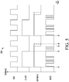
- FIG. 5 illustrates, in simplified timing diagram form, example signal timing 500 of clock duty cycle control circuit of FIG. 2 in accordance with an embodiment.
- Signal timing 500 includes source clock signal CLK, example 50% duty cycle clock signal CLK50, asymmetrical clock signal ASYMCLK, and example data signal DATA waveforms.
- the example implementation of the asymmetrical clock generator 202 as depicted in FIG. 3 includes counter-based divider circuitry 302 and a phase delay circuitry 304 for generating a divide-by 3 asymmetrical clock signal ASYMCLK.
- the ASYMCLK waveform is shown having a counter-based divided-by 3 active portion from time marker t1 to t3 and a phase delayed portion from time marker t3 to t4.
- the phase delayed portion may range from 0% to 10% for fine adjustments to the duty cycle of ASYMCLK.
- the CLK50 signal is shown as a 50% duty cycle version of a divide-by 3 clock having an active phase (e.g., logic high level from time marker t1 to t2) approximately equal to 50% of the cycle time (e.g., from time marker t1 to t5).
- the data signal DATA is shown transitioning from a logic low value to a logic high value and back to the logic low value several times from time marker t1 to t3.
- the DATA signal may represent example data signals D1-D3 generated in respective logic circuits 210-214.
- the data signals D1-D3 may include several transitions like those shown in the DATA signal.
- Storage elements such as flip flops are typically clocked by a 50% duty cycle clock like CLK50. However, intermediate data transitions may occur while the master portion of the flip flops are transparent allowing the intermediate data transitions like those from timing marker t2 to t3 of the DATA waveform to propagate through the master portion. Accordingly, unwanted power consumption can occur.
- storage elements 204-208 are clocked by the ASYMCLK signal, the intermediate data transitions occur while the master circuit portion is non-transparent, thus resulting in significant power savings.
- an integrated circuit that includes asymmetrical clock generation circuitry coupled to provide to an asymmetrical clock to one or more storage elements configured in a master-slave arrangement.
- the asymmetrical clock is generated having a predetermined duty cycle greater than 50% such that intermediate data transitions are inhibited from propagating through master portions of the storage elements. By inhibiting the intermediate data transitions from propagating through the master portions, significant power savings can be realized.
- an integrated circuit including a first master-slave storage element having a data input coupled to receive a data signal; and an asymmetrical clock generator coupled to provide an asymmetrical clock signal to the first master-slave storage element, a first phase of the asymmetrical clock signal configured for inhibiting intermediate data signal transitions from propagating through the master portion of the first master-slave storage element.
- the asymmetrical clock generator may be configured to generate the first phase having a range of 60% to 80% of the asymmetrical clock cycle.
- the asymmetrical clock generator may include circuitry to generate the first phase of the asymmetrical clock such that the first phase tracks process, voltage, and temperature.
- the asymmetrical clock generator may include a counter-based divider circuit.
- the asymmetrical clock generator may include a phase delay circuit.
- the first master-slave storage element may be characterized as a D-type flip flop or D flip flop.
- the first master-slave storage element may be characterized as a state retention flip flop having the slave portion supplied by a voltage supply different from the master portion.
- the integrated circuit may further include a second master-slave storage element having a clock input coupled to receive the asymmetrical clock signal.
- the integrated circuit may further include a logic circuit coupled between an output of the first master-slave storage element and a data input of the second master-slave storage element, the first phase of the asymmetrical clock signal further configured for inhibiting intermediate data signal transitions from propagating through the master portion of the second master-slave storage element.
- an integrated circuit including a first storage element having a master circuit and a slave circuit, the master circuit configured to be transparent during a first phase of a clock signal; and an asymmetrical clock generator coupled to provide the clock signal to the first storage element, the first phase of the clock signal configured to be longer than a second phase of the clock signal.
- the asymmetrical clock generator may be configured to provide the clock signal based on a counter-based divider circuit output signal.
- the asymmetrical clock generator may be configured to provide the clock signal based on a phase delay circuit output signal.
- the asymmetrical clock generator may be configured to generate the clock signal having a duty cycle in a range of 60% to 80%.
- the asymmetrical clock generator may include circuitry to generate the first phase of the clock such that the first phase tracks process, voltage, and temperature.
- the first storage element may be characterized as a D-type flip flop or D flip flop.
- the integrated circuit may further include a logic circuit coupled between an output of the first storage element and a data input of a second storage element, the second storage element having a clock input coupled to receive the clock signal.
- an integrated circuit including a first storage element having a master circuit and a slave circuit, the master circuit coupled to receive a data signal and configured to be transparent during a first phase of a clock signal; and an asymmetrical clock generator coupled to provide the clock signal to the first storage element, the first phase of the clock signal configured for inhibiting intermediate data signal transitions from propagating through the master circuit.
- the asymmetrical clock generator may be configured to generate the clock signal having a duty cycle in a range of 60% to 80%.
- the asymmetrical clock generator may be configured to provide the clock signal based on a counter-based divider circuit output signal.
- the integrated circuit may further include a logic circuit coupled between an output of the first storage element and a data input of a second storage element, the second storage element having a clock input coupled to receive the clock signal.
- Each signal described herein may be designed as positive or negative logic.
- the signal In the case of a negative logic signal, the signal is active low where the logically true state corresponds to a logic level zero.
- the signal In the case of a positive logic signal, the signal is active high where the logically true state corresponds to a logic level one.
- any of the signals described herein can be designed as either negative or positive logic signals. Therefore, in alternate embodiments, those signals described as positive logic signals may be implemented as negative logic signals, and those signals described as negative logic signals may be implemented as positive logic signals.
- An integrated circuit includes a master-slave storage element having a data input coupled to receive a data signal and an asymmetrical clock generator coupled to provide an asymmetrical clock signal to the master-slave storage element.
- a first phase of the asymmetrical clock signal is configured for inhibiting intermediate data signal transitions from propagating through the master portion of the master-slave storage element.
Landscapes
- Engineering & Computer Science (AREA)
- Theoretical Computer Science (AREA)
- Physics & Mathematics (AREA)
- General Engineering & Computer Science (AREA)
- General Physics & Mathematics (AREA)
- Computer Hardware Design (AREA)
- Computing Systems (AREA)
- Mathematical Physics (AREA)
- Pulse Circuits (AREA)
- Manipulation Of Pulses (AREA)
Applications Claiming Priority (1)
| Application Number | Priority Date | Filing Date | Title |
|---|---|---|---|
| US16/219,029 US11048292B2 (en) | 2018-12-13 | 2018-12-13 | Duty cycle control for reduced dynamic power consumption |
Publications (3)
| Publication Number | Publication Date |
|---|---|
| EP3667910A2 true EP3667910A2 (de) | 2020-06-17 |
| EP3667910A3 EP3667910A3 (de) | 2020-08-12 |
| EP3667910B1 EP3667910B1 (de) | 2025-08-27 |
Family
ID=68732665
Family Applications (1)
| Application Number | Title | Priority Date | Filing Date |
|---|---|---|---|
| EP19210142.6A Active EP3667910B1 (de) | 2018-12-13 | 2019-11-19 | Tastverhältnissteuerung für reduzierten dynamischen stromverbrauch |
Country Status (2)
| Country | Link |
|---|---|
| US (1) | US11048292B2 (de) |
| EP (1) | EP3667910B1 (de) |
Citations (1)
| Publication number | Priority date | Publication date | Assignee | Title |
|---|---|---|---|---|
| US8253463B1 (en) * | 2010-03-10 | 2012-08-28 | Altera Corporation | Pulse width control circuitry |
Family Cites Families (9)
| Publication number | Priority date | Publication date | Assignee | Title |
|---|---|---|---|---|
| US4104860A (en) | 1976-12-27 | 1978-08-08 | Solid State Scientific Inc. | High speed dynamic flip-flop system |
| US4885758A (en) * | 1988-06-06 | 1989-12-05 | Hayes Microcomputer Products, Inc. | Speed correction and stop bit control circuit for data communications device |
| US6668357B2 (en) | 2001-06-29 | 2003-12-23 | Fujitsu Limited | Cold clock power reduction |
| US6977528B2 (en) | 2002-09-03 | 2005-12-20 | The Regents Of The University Of California | Event driven dynamic logic for reducing power consumption |
| US7342425B1 (en) * | 2005-09-07 | 2008-03-11 | National Semiconductor Corporation | Method and apparatus for a symmetrical odd-number clock divider |
| US8542522B2 (en) * | 2009-07-23 | 2013-09-24 | Hewlett-Packard Development Company, L.P. | Non-volatile data-storage latch |
| TWI543540B (zh) | 2014-01-06 | 2016-07-21 | 南亞科技股份有限公司 | 積體電路以及調整其工作週期的方法 |
| US9325323B2 (en) | 2014-08-30 | 2016-04-26 | Stmicroelectronics International N.V. | CMOS oscillator having stable frequency with process, temperature, and voltage variation |
| US10719387B2 (en) * | 2018-04-25 | 2020-07-21 | Oracle International Corporation | Memory interface with tamper-evident features to enhance software security |
-
2018
- 2018-12-13 US US16/219,029 patent/US11048292B2/en active Active
-
2019
- 2019-11-19 EP EP19210142.6A patent/EP3667910B1/de active Active
Patent Citations (1)
| Publication number | Priority date | Publication date | Assignee | Title |
|---|---|---|---|---|
| US8253463B1 (en) * | 2010-03-10 | 2012-08-28 | Altera Corporation | Pulse width control circuitry |
Also Published As
| Publication number | Publication date |
|---|---|
| US11048292B2 (en) | 2021-06-29 |
| EP3667910A3 (de) | 2020-08-12 |
| US20200192419A1 (en) | 2020-06-18 |
| EP3667910B1 (de) | 2025-08-27 |
Similar Documents
| Publication | Publication Date | Title |
|---|---|---|
| US5914996A (en) | Multiple clock frequency divider with fifty percent duty cycle output | |
| US9742382B2 (en) | Flip-flop for reducing dynamic power | |
| KR100398480B1 (ko) | 디엘엘 회로, 이를 사용하는 반도체 장치 및 지연 제어 방법 | |
| US7652517B2 (en) | Method and apparatus for generating synchronous clock signals from a common clock signal | |
| CN103166602A (zh) | 低功耗的主从触发器 | |
| EP0851581A2 (de) | Kippschaltung | |
| KR20090035592A (ko) | 클럭 에지 복원을 갖는 펄스 카운터 | |
| US20180054203A1 (en) | Wide Range Glitchless Switchable Clock Divider With Modified 2/3 Divider Stages | |
| JP3851113B2 (ja) | デスキュー回路を有するクロック生成器 | |
| JPH10117127A (ja) | 論理記憶回路及び論理回路 | |
| US7109776B2 (en) | Gating for dual edge-triggered clocking | |
| US9372499B2 (en) | Low insertion delay clock doubler and integrated circuit clock distribution system using same | |
| US7881422B1 (en) | Circuits and methods for dividing frequency by an odd value | |
| CN111697965B (zh) | 高速相位频率检测器 | |
| JPH07210267A (ja) | 集積回路およびデータ処理装置 | |
| EP3667910B1 (de) | Tastverhältnissteuerung für reduzierten dynamischen stromverbrauch | |
| JPH0946189A (ja) | クロック供給回路 | |
| US5045715A (en) | Circuit for generating stretched clock phases on a cycle by cycle basis | |
| US8466720B2 (en) | Frequency division of an input clock signal | |
| US7049864B2 (en) | Apparatus and method for high frequency state machine divider with low power consumption | |
| US6252449B1 (en) | Clock distribution circuit in an integrated circuit | |
| US5969548A (en) | Frequency divider with low power consumption | |
| US20210184657A1 (en) | Apparatus for Asynchronous Latch with Improved Performance and Associated Methods | |
| US6441666B1 (en) | System and method for generating clock signals | |
| JPS6253968B2 (de) |
Legal Events
| Date | Code | Title | Description |
|---|---|---|---|
| PUAI | Public reference made under article 153(3) epc to a published international application that has entered the european phase |
Free format text: ORIGINAL CODE: 0009012 |
|
| STAA | Information on the status of an ep patent application or granted ep patent |
Free format text: STATUS: THE APPLICATION HAS BEEN PUBLISHED |
|
| AK | Designated contracting states |
Kind code of ref document: A2 Designated state(s): AL AT BE BG CH CY CZ DE DK EE ES FI FR GB GR HR HU IE IS IT LI LT LU LV MC MK MT NL NO PL PT RO RS SE SI SK SM TR |
|
| AX | Request for extension of the european patent |
Extension state: BA ME |
|
| PUAL | Search report despatched |
Free format text: ORIGINAL CODE: 0009013 |
|
| AK | Designated contracting states |
Kind code of ref document: A3 Designated state(s): AL AT BE BG CH CY CZ DE DK EE ES FI FR GB GR HR HU IE IS IT LI LT LU LV MC MK MT NL NO PL PT RO RS SE SI SK SM TR |
|
| AX | Request for extension of the european patent |
Extension state: BA ME |
|
| RIC1 | Information provided on ipc code assigned before grant |
Ipc: H03K 3/037 20060101ALI20200706BHEP Ipc: H03K 3/3562 20060101ALI20200706BHEP Ipc: H03K 3/012 20060101AFI20200706BHEP Ipc: H03K 3/017 20060101ALI20200706BHEP |
|
| STAA | Information on the status of an ep patent application or granted ep patent |
Free format text: STATUS: REQUEST FOR EXAMINATION WAS MADE |
|
| 17P | Request for examination filed |
Effective date: 20210212 |
|
| RBV | Designated contracting states (corrected) |
Designated state(s): AL AT BE BG CH CY CZ DE DK EE ES FI FR GB GR HR HU IE IS IT LI LT LU LV MC MK MT NL NO PL PT RO RS SE SI SK SM TR |
|
| STAA | Information on the status of an ep patent application or granted ep patent |
Free format text: STATUS: EXAMINATION IS IN PROGRESS |
|
| 17Q | First examination report despatched |
Effective date: 20221219 |
|
| GRAP | Despatch of communication of intention to grant a patent |
Free format text: ORIGINAL CODE: EPIDOSNIGR1 |
|
| STAA | Information on the status of an ep patent application or granted ep patent |
Free format text: STATUS: GRANT OF PATENT IS INTENDED |
|
| INTG | Intention to grant announced |
Effective date: 20250321 |
|
| GRAS | Grant fee paid |
Free format text: ORIGINAL CODE: EPIDOSNIGR3 |
|
| GRAA | (expected) grant |
Free format text: ORIGINAL CODE: 0009210 |
|
| STAA | Information on the status of an ep patent application or granted ep patent |
Free format text: STATUS: THE PATENT HAS BEEN GRANTED |
|
| AK | Designated contracting states |
Kind code of ref document: B1 Designated state(s): AL AT BE BG CH CY CZ DE DK EE ES FI FR GB GR HR HU IE IS IT LI LT LU LV MC MK MT NL NO PL PT RO RS SE SI SK SM TR |
|
| REG | Reference to a national code |
Ref country code: GB Ref legal event code: FG4D |
|
| REG | Reference to a national code |
Ref country code: CH Ref legal event code: EP |
|
| REG | Reference to a national code |
Ref country code: DE Ref legal event code: R096 Ref document number: 602019074672 Country of ref document: DE |
|
| REG | Reference to a national code |
Ref country code: IE Ref legal event code: FG4D |
|
| REG | Reference to a national code |
Ref country code: NL Ref legal event code: MP Effective date: 20250827 |
|
| PG25 | Lapsed in a contracting state [announced via postgrant information from national office to epo] |
Ref country code: IS Free format text: LAPSE BECAUSE OF FAILURE TO SUBMIT A TRANSLATION OF THE DESCRIPTION OR TO PAY THE FEE WITHIN THE PRESCRIBED TIME-LIMIT Effective date: 20251227 |
|
| PGFP | Annual fee paid to national office [announced via postgrant information from national office to epo] |
Ref country code: DE Payment date: 20251022 Year of fee payment: 7 |
|
| PG25 | Lapsed in a contracting state [announced via postgrant information from national office to epo] |
Ref country code: NO Free format text: LAPSE BECAUSE OF FAILURE TO SUBMIT A TRANSLATION OF THE DESCRIPTION OR TO PAY THE FEE WITHIN THE PRESCRIBED TIME-LIMIT Effective date: 20251127 |
|
| REG | Reference to a national code |
Ref country code: LT Ref legal event code: MG9D |
|
| PG25 | Lapsed in a contracting state [announced via postgrant information from national office to epo] |
Ref country code: PT Free format text: LAPSE BECAUSE OF FAILURE TO SUBMIT A TRANSLATION OF THE DESCRIPTION OR TO PAY THE FEE WITHIN THE PRESCRIBED TIME-LIMIT Effective date: 20251229 |
|
| PG25 | Lapsed in a contracting state [announced via postgrant information from national office to epo] |
Ref country code: FI Free format text: LAPSE BECAUSE OF FAILURE TO SUBMIT A TRANSLATION OF THE DESCRIPTION OR TO PAY THE FEE WITHIN THE PRESCRIBED TIME-LIMIT Effective date: 20250827 |
|
| PG25 | Lapsed in a contracting state [announced via postgrant information from national office to epo] |
Ref country code: HR Free format text: LAPSE BECAUSE OF FAILURE TO SUBMIT A TRANSLATION OF THE DESCRIPTION OR TO PAY THE FEE WITHIN THE PRESCRIBED TIME-LIMIT Effective date: 20250827 Ref country code: NL Free format text: LAPSE BECAUSE OF FAILURE TO SUBMIT A TRANSLATION OF THE DESCRIPTION OR TO PAY THE FEE WITHIN THE PRESCRIBED TIME-LIMIT Effective date: 20250827 |
|
| PG25 | Lapsed in a contracting state [announced via postgrant information from national office to epo] |
Ref country code: GR Free format text: LAPSE BECAUSE OF FAILURE TO SUBMIT A TRANSLATION OF THE DESCRIPTION OR TO PAY THE FEE WITHIN THE PRESCRIBED TIME-LIMIT Effective date: 20251128 |
|
| PG25 | Lapsed in a contracting state [announced via postgrant information from national office to epo] |
Ref country code: SE Free format text: LAPSE BECAUSE OF FAILURE TO SUBMIT A TRANSLATION OF THE DESCRIPTION OR TO PAY THE FEE WITHIN THE PRESCRIBED TIME-LIMIT Effective date: 20250827 |
|
| PG25 | Lapsed in a contracting state [announced via postgrant information from national office to epo] |
Ref country code: LV Free format text: LAPSE BECAUSE OF FAILURE TO SUBMIT A TRANSLATION OF THE DESCRIPTION OR TO PAY THE FEE WITHIN THE PRESCRIBED TIME-LIMIT Effective date: 20250827 |
|
| PG25 | Lapsed in a contracting state [announced via postgrant information from national office to epo] |
Ref country code: PL Free format text: LAPSE BECAUSE OF FAILURE TO SUBMIT A TRANSLATION OF THE DESCRIPTION OR TO PAY THE FEE WITHIN THE PRESCRIBED TIME-LIMIT Effective date: 20250827 Ref country code: BG Free format text: LAPSE BECAUSE OF FAILURE TO SUBMIT A TRANSLATION OF THE DESCRIPTION OR TO PAY THE FEE WITHIN THE PRESCRIBED TIME-LIMIT Effective date: 20250827 |
|
| PG25 | Lapsed in a contracting state [announced via postgrant information from national office to epo] |
Ref country code: RS Free format text: LAPSE BECAUSE OF FAILURE TO SUBMIT A TRANSLATION OF THE DESCRIPTION OR TO PAY THE FEE WITHIN THE PRESCRIBED TIME-LIMIT Effective date: 20251127 |
|
| PG25 | Lapsed in a contracting state [announced via postgrant information from national office to epo] |
Ref country code: ES Free format text: LAPSE BECAUSE OF FAILURE TO SUBMIT A TRANSLATION OF THE DESCRIPTION OR TO PAY THE FEE WITHIN THE PRESCRIBED TIME-LIMIT Effective date: 20250827 |
|
| REG | Reference to a national code |
Ref country code: AT Ref legal event code: MK05 Ref document number: 1831224 Country of ref document: AT Kind code of ref document: T Effective date: 20250827 |
|
| PG25 | Lapsed in a contracting state [announced via postgrant information from national office to epo] |
Ref country code: RO Free format text: LAPSE BECAUSE OF FAILURE TO SUBMIT A TRANSLATION OF THE DESCRIPTION OR TO PAY THE FEE WITHIN THE PRESCRIBED TIME-LIMIT Effective date: 20250827 |
|
| PG25 | Lapsed in a contracting state [announced via postgrant information from national office to epo] |
Ref country code: SM Free format text: LAPSE BECAUSE OF FAILURE TO SUBMIT A TRANSLATION OF THE DESCRIPTION OR TO PAY THE FEE WITHIN THE PRESCRIBED TIME-LIMIT Effective date: 20250827 |
|
| PG25 | Lapsed in a contracting state [announced via postgrant information from national office to epo] |
Ref country code: DK Free format text: LAPSE BECAUSE OF FAILURE TO SUBMIT A TRANSLATION OF THE DESCRIPTION OR TO PAY THE FEE WITHIN THE PRESCRIBED TIME-LIMIT Effective date: 20250827 |
|
| PG25 | Lapsed in a contracting state [announced via postgrant information from national office to epo] |
Ref country code: AT Free format text: LAPSE BECAUSE OF FAILURE TO SUBMIT A TRANSLATION OF THE DESCRIPTION OR TO PAY THE FEE WITHIN THE PRESCRIBED TIME-LIMIT Effective date: 20250827 |
|
| PG25 | Lapsed in a contracting state [announced via postgrant information from national office to epo] |
Ref country code: IT Free format text: LAPSE BECAUSE OF FAILURE TO SUBMIT A TRANSLATION OF THE DESCRIPTION OR TO PAY THE FEE WITHIN THE PRESCRIBED TIME-LIMIT Effective date: 20250827 |
|
| PG25 | Lapsed in a contracting state [announced via postgrant information from national office to epo] |
Ref country code: CZ Free format text: LAPSE BECAUSE OF FAILURE TO SUBMIT A TRANSLATION OF THE DESCRIPTION OR TO PAY THE FEE WITHIN THE PRESCRIBED TIME-LIMIT Effective date: 20250827 |
|
| PG25 | Lapsed in a contracting state [announced via postgrant information from national office to epo] |
Ref country code: SK Free format text: LAPSE BECAUSE OF FAILURE TO SUBMIT A TRANSLATION OF THE DESCRIPTION OR TO PAY THE FEE WITHIN THE PRESCRIBED TIME-LIMIT Effective date: 20250827 Ref country code: EE Free format text: LAPSE BECAUSE OF FAILURE TO SUBMIT A TRANSLATION OF THE DESCRIPTION OR TO PAY THE FEE WITHIN THE PRESCRIBED TIME-LIMIT Effective date: 20250827 |