EP3667831A1 - Steckverbinderteil mit einer leiterplatte - Google Patents
Steckverbinderteil mit einer leiterplatte Download PDFInfo
- Publication number
- EP3667831A1 EP3667831A1 EP19209323.5A EP19209323A EP3667831A1 EP 3667831 A1 EP3667831 A1 EP 3667831A1 EP 19209323 A EP19209323 A EP 19209323A EP 3667831 A1 EP3667831 A1 EP 3667831A1
- Authority
- EP
- European Patent Office
- Prior art keywords
- contact
- circuit board
- connector part
- printed circuit
- contact element
- Prior art date
- Legal status (The legal status is an assumption and is not a legal conclusion. Google has not performed a legal analysis and makes no representation as to the accuracy of the status listed.)
- Granted
Links
- 230000013011 mating Effects 0.000 claims abstract description 25
- 238000010438 heat treatment Methods 0.000 claims description 4
- 230000000149 penetrating effect Effects 0.000 claims 1
- 230000008878 coupling Effects 0.000 description 6
- 238000010168 coupling process Methods 0.000 description 6
- 238000005859 coupling reaction Methods 0.000 description 6
- 238000012544 monitoring process Methods 0.000 description 6
- 238000002788 crimping Methods 0.000 description 2
- 238000000034 method Methods 0.000 description 2
- 230000006978 adaptation Effects 0.000 description 1
- 230000000712 assembly Effects 0.000 description 1
- 238000000429 assembly Methods 0.000 description 1
- 230000005540 biological transmission Effects 0.000 description 1
- 239000000919 ceramic Substances 0.000 description 1
- 229910010293 ceramic material Inorganic materials 0.000 description 1
- 239000004020 conductor Substances 0.000 description 1
- 230000007423 decrease Effects 0.000 description 1
- 230000001419 dependent effect Effects 0.000 description 1
- 238000001514 detection method Methods 0.000 description 1
- 230000000694 effects Effects 0.000 description 1
- 230000005611 electricity Effects 0.000 description 1
- 238000003780 insertion Methods 0.000 description 1
- 230000037431 insertion Effects 0.000 description 1
- 238000004519 manufacturing process Methods 0.000 description 1
- 239000000463 material Substances 0.000 description 1
- 238000012986 modification Methods 0.000 description 1
- 230000004048 modification Effects 0.000 description 1
- 238000013021 overheating Methods 0.000 description 1
- 230000001681 protective effect Effects 0.000 description 1
- 239000004065 semiconductor Substances 0.000 description 1
Images


Classifications
-
- H—ELECTRICITY
- H01—ELECTRIC ELEMENTS
- H01R—ELECTRICALLY-CONDUCTIVE CONNECTIONS; STRUCTURAL ASSOCIATIONS OF A PLURALITY OF MUTUALLY-INSULATED ELECTRICAL CONNECTING ELEMENTS; COUPLING DEVICES; CURRENT COLLECTORS
- H01R13/00—Details of coupling devices of the kinds covered by groups H01R12/70 or H01R24/00 - H01R33/00
- H01R13/66—Structural association with built-in electrical component
- H01R13/665—Structural association with built-in electrical component with built-in electronic circuit
- H01R13/6658—Structural association with built-in electrical component with built-in electronic circuit on printed circuit board
-
- H—ELECTRICITY
- H01—ELECTRIC ELEMENTS
- H01R—ELECTRICALLY-CONDUCTIVE CONNECTIONS; STRUCTURAL ASSOCIATIONS OF A PLURALITY OF MUTUALLY-INSULATED ELECTRICAL CONNECTING ELEMENTS; COUPLING DEVICES; CURRENT COLLECTORS
- H01R12/00—Structural associations of a plurality of mutually-insulated electrical connecting elements, specially adapted for printed circuits, e.g. printed circuit boards [PCB], flat or ribbon cables, or like generally planar structures, e.g. terminal strips, terminal blocks; Coupling devices specially adapted for printed circuits, flat or ribbon cables, or like generally planar structures; Terminals specially adapted for contact with, or insertion into, printed circuits, flat or ribbon cables, or like generally planar structures
- H01R12/50—Fixed connections
- H01R12/51—Fixed connections for rigid printed circuits or like structures
- H01R12/55—Fixed connections for rigid printed circuits or like structures characterised by the terminals
- H01R12/58—Fixed connections for rigid printed circuits or like structures characterised by the terminals terminals for insertion into holes
- H01R12/585—Terminals having a press fit or a compliant portion and a shank passing through a hole in the printed circuit board
-
- B—PERFORMING OPERATIONS; TRANSPORTING
- B60—VEHICLES IN GENERAL
- B60L—PROPULSION OF ELECTRICALLY-PROPELLED VEHICLES; SUPPLYING ELECTRIC POWER FOR AUXILIARY EQUIPMENT OF ELECTRICALLY-PROPELLED VEHICLES; ELECTRODYNAMIC BRAKE SYSTEMS FOR VEHICLES IN GENERAL; MAGNETIC SUSPENSION OR LEVITATION FOR VEHICLES; MONITORING OPERATING VARIABLES OF ELECTRICALLY-PROPELLED VEHICLES; ELECTRIC SAFETY DEVICES FOR ELECTRICALLY-PROPELLED VEHICLES
- B60L53/00—Methods of charging batteries, specially adapted for electric vehicles; Charging stations or on-board charging equipment therefor; Exchange of energy storage elements in electric vehicles
- B60L53/10—Methods of charging batteries, specially adapted for electric vehicles; Charging stations or on-board charging equipment therefor; Exchange of energy storage elements in electric vehicles characterised by the energy transfer between the charging station and the vehicle
- B60L53/14—Conductive energy transfer
- B60L53/16—Connectors, e.g. plugs or sockets, specially adapted for charging electric vehicles
-
- B—PERFORMING OPERATIONS; TRANSPORTING
- B60—VEHICLES IN GENERAL
- B60L—PROPULSION OF ELECTRICALLY-PROPELLED VEHICLES; SUPPLYING ELECTRIC POWER FOR AUXILIARY EQUIPMENT OF ELECTRICALLY-PROPELLED VEHICLES; ELECTRODYNAMIC BRAKE SYSTEMS FOR VEHICLES IN GENERAL; MAGNETIC SUSPENSION OR LEVITATION FOR VEHICLES; MONITORING OPERATING VARIABLES OF ELECTRICALLY-PROPELLED VEHICLES; ELECTRIC SAFETY DEVICES FOR ELECTRICALLY-PROPELLED VEHICLES
- B60L53/00—Methods of charging batteries, specially adapted for electric vehicles; Charging stations or on-board charging equipment therefor; Exchange of energy storage elements in electric vehicles
- B60L53/60—Monitoring or controlling charging stations
- B60L53/62—Monitoring or controlling charging stations in response to charging parameters, e.g. current, voltage or electrical charge
-
- H—ELECTRICITY
- H01—ELECTRIC ELEMENTS
- H01R—ELECTRICALLY-CONDUCTIVE CONNECTIONS; STRUCTURAL ASSOCIATIONS OF A PLURALITY OF MUTUALLY-INSULATED ELECTRICAL CONNECTING ELEMENTS; COUPLING DEVICES; CURRENT COLLECTORS
- H01R13/00—Details of coupling devices of the kinds covered by groups H01R12/70 or H01R24/00 - H01R33/00
- H01R13/02—Contact members
- H01R13/22—Contacts for co-operating by abutting
- H01R13/24—Contacts for co-operating by abutting resilient; resiliently-mounted
-
- H—ELECTRICITY
- H01—ELECTRIC ELEMENTS
- H01R—ELECTRICALLY-CONDUCTIVE CONNECTIONS; STRUCTURAL ASSOCIATIONS OF A PLURALITY OF MUTUALLY-INSULATED ELECTRICAL CONNECTING ELEMENTS; COUPLING DEVICES; CURRENT COLLECTORS
- H01R13/00—Details of coupling devices of the kinds covered by groups H01R12/70 or H01R24/00 - H01R33/00
- H01R13/46—Bases; Cases
- H01R13/50—Bases; Cases formed as an integral body
-
- H—ELECTRICITY
- H01—ELECTRIC ELEMENTS
- H01R—ELECTRICALLY-CONDUCTIVE CONNECTIONS; STRUCTURAL ASSOCIATIONS OF A PLURALITY OF MUTUALLY-INSULATED ELECTRICAL CONNECTING ELEMENTS; COUPLING DEVICES; CURRENT COLLECTORS
- H01R13/00—Details of coupling devices of the kinds covered by groups H01R12/70 or H01R24/00 - H01R33/00
- H01R13/66—Structural association with built-in electrical component
- H01R13/6608—Structural association with built-in electrical component with built-in single component
- H01R13/6616—Structural association with built-in electrical component with built-in single component with resistor
-
- H—ELECTRICITY
- H01—ELECTRIC ELEMENTS
- H01R—ELECTRICALLY-CONDUCTIVE CONNECTIONS; STRUCTURAL ASSOCIATIONS OF A PLURALITY OF MUTUALLY-INSULATED ELECTRICAL CONNECTING ELEMENTS; COUPLING DEVICES; CURRENT COLLECTORS
- H01R13/00—Details of coupling devices of the kinds covered by groups H01R12/70 or H01R24/00 - H01R33/00
- H01R13/66—Structural association with built-in electrical component
- H01R13/665—Structural association with built-in electrical component with built-in electronic circuit
- H01R13/6683—Structural association with built-in electrical component with built-in electronic circuit with built-in sensor
-
- H—ELECTRICITY
- H05—ELECTRIC TECHNIQUES NOT OTHERWISE PROVIDED FOR
- H05K—PRINTED CIRCUITS; CASINGS OR CONSTRUCTIONAL DETAILS OF ELECTRIC APPARATUS; MANUFACTURE OF ASSEMBLAGES OF ELECTRICAL COMPONENTS
- H05K1/00—Printed circuits
- H05K1/18—Printed circuits structurally associated with non-printed electric components
-
- B—PERFORMING OPERATIONS; TRANSPORTING
- B60—VEHICLES IN GENERAL
- B60L—PROPULSION OF ELECTRICALLY-PROPELLED VEHICLES; SUPPLYING ELECTRIC POWER FOR AUXILIARY EQUIPMENT OF ELECTRICALLY-PROPELLED VEHICLES; ELECTRODYNAMIC BRAKE SYSTEMS FOR VEHICLES IN GENERAL; MAGNETIC SUSPENSION OR LEVITATION FOR VEHICLES; MONITORING OPERATING VARIABLES OF ELECTRICALLY-PROPELLED VEHICLES; ELECTRIC SAFETY DEVICES FOR ELECTRICALLY-PROPELLED VEHICLES
- B60L53/00—Methods of charging batteries, specially adapted for electric vehicles; Charging stations or on-board charging equipment therefor; Exchange of energy storage elements in electric vehicles
- B60L53/10—Methods of charging batteries, specially adapted for electric vehicles; Charging stations or on-board charging equipment therefor; Exchange of energy storage elements in electric vehicles characterised by the energy transfer between the charging station and the vehicle
- B60L53/14—Conductive energy transfer
- B60L53/18—Cables specially adapted for charging electric vehicles
-
- H—ELECTRICITY
- H01—ELECTRIC ELEMENTS
- H01R—ELECTRICALLY-CONDUCTIVE CONNECTIONS; STRUCTURAL ASSOCIATIONS OF A PLURALITY OF MUTUALLY-INSULATED ELECTRICAL CONNECTING ELEMENTS; COUPLING DEVICES; CURRENT COLLECTORS
- H01R12/00—Structural associations of a plurality of mutually-insulated electrical connecting elements, specially adapted for printed circuits, e.g. printed circuit boards [PCB], flat or ribbon cables, or like generally planar structures, e.g. terminal strips, terminal blocks; Coupling devices specially adapted for printed circuits, flat or ribbon cables, or like generally planar structures; Terminals specially adapted for contact with, or insertion into, printed circuits, flat or ribbon cables, or like generally planar structures
- H01R12/50—Fixed connections
- H01R12/51—Fixed connections for rigid printed circuits or like structures
- H01R12/55—Fixed connections for rigid printed circuits or like structures characterised by the terminals
- H01R12/57—Fixed connections for rigid printed circuits or like structures characterised by the terminals surface mounting terminals
-
- H—ELECTRICITY
- H01—ELECTRIC ELEMENTS
- H01R—ELECTRICALLY-CONDUCTIVE CONNECTIONS; STRUCTURAL ASSOCIATIONS OF A PLURALITY OF MUTUALLY-INSULATED ELECTRICAL CONNECTING ELEMENTS; COUPLING DEVICES; CURRENT COLLECTORS
- H01R12/00—Structural associations of a plurality of mutually-insulated electrical connecting elements, specially adapted for printed circuits, e.g. printed circuit boards [PCB], flat or ribbon cables, or like generally planar structures, e.g. terminal strips, terminal blocks; Coupling devices specially adapted for printed circuits, flat or ribbon cables, or like generally planar structures; Terminals specially adapted for contact with, or insertion into, printed circuits, flat or ribbon cables, or like generally planar structures
- H01R12/70—Coupling devices
- H01R12/71—Coupling devices for rigid printing circuits or like structures
- H01R12/712—Coupling devices for rigid printing circuits or like structures co-operating with the surface of the printed circuit or with a coupling device exclusively provided on the surface of the printed circuit
- H01R12/714—Coupling devices for rigid printing circuits or like structures co-operating with the surface of the printed circuit or with a coupling device exclusively provided on the surface of the printed circuit with contacts abutting directly the printed circuit; Button contacts therefore provided on the printed circuit
-
- H—ELECTRICITY
- H01—ELECTRIC ELEMENTS
- H01R—ELECTRICALLY-CONDUCTIVE CONNECTIONS; STRUCTURAL ASSOCIATIONS OF A PLURALITY OF MUTUALLY-INSULATED ELECTRICAL CONNECTING ELEMENTS; COUPLING DEVICES; CURRENT COLLECTORS
- H01R2201/00—Connectors or connections adapted for particular applications
- H01R2201/26—Connectors or connections adapted for particular applications for vehicles
-
- H—ELECTRICITY
- H05—ELECTRIC TECHNIQUES NOT OTHERWISE PROVIDED FOR
- H05K—PRINTED CIRCUITS; CASINGS OR CONSTRUCTIONAL DETAILS OF ELECTRIC APPARATUS; MANUFACTURE OF ASSEMBLAGES OF ELECTRICAL COMPONENTS
- H05K2201/00—Indexing scheme relating to printed circuits covered by H05K1/00
- H05K2201/09—Shape and layout
- H05K2201/09009—Substrate related
- H05K2201/09027—Non-rectangular flat PCB, e.g. circular
-
- H—ELECTRICITY
- H05—ELECTRIC TECHNIQUES NOT OTHERWISE PROVIDED FOR
- H05K—PRINTED CIRCUITS; CASINGS OR CONSTRUCTIONAL DETAILS OF ELECTRIC APPARATUS; MANUFACTURE OF ASSEMBLAGES OF ELECTRICAL COMPONENTS
- H05K2201/00—Indexing scheme relating to printed circuits covered by H05K1/00
- H05K2201/10—Details of components or other objects attached to or integrated in a printed circuit board
- H05K2201/10007—Types of components
- H05K2201/10022—Non-printed resistor
-
- H—ELECTRICITY
- H05—ELECTRIC TECHNIQUES NOT OTHERWISE PROVIDED FOR
- H05K—PRINTED CIRCUITS; CASINGS OR CONSTRUCTIONAL DETAILS OF ELECTRIC APPARATUS; MANUFACTURE OF ASSEMBLAGES OF ELECTRICAL COMPONENTS
- H05K2201/00—Indexing scheme relating to printed circuits covered by H05K1/00
- H05K2201/10—Details of components or other objects attached to or integrated in a printed circuit board
- H05K2201/10007—Types of components
- H05K2201/10151—Sensor
-
- Y—GENERAL TAGGING OF NEW TECHNOLOGICAL DEVELOPMENTS; GENERAL TAGGING OF CROSS-SECTIONAL TECHNOLOGIES SPANNING OVER SEVERAL SECTIONS OF THE IPC; TECHNICAL SUBJECTS COVERED BY FORMER USPC CROSS-REFERENCE ART COLLECTIONS [XRACs] AND DIGESTS
- Y02—TECHNOLOGIES OR APPLICATIONS FOR MITIGATION OR ADAPTATION AGAINST CLIMATE CHANGE
- Y02T—CLIMATE CHANGE MITIGATION TECHNOLOGIES RELATED TO TRANSPORTATION
- Y02T10/00—Road transport of goods or passengers
- Y02T10/60—Other road transportation technologies with climate change mitigation effect
- Y02T10/70—Energy storage systems for electromobility, e.g. batteries
-
- Y—GENERAL TAGGING OF NEW TECHNOLOGICAL DEVELOPMENTS; GENERAL TAGGING OF CROSS-SECTIONAL TECHNOLOGIES SPANNING OVER SEVERAL SECTIONS OF THE IPC; TECHNICAL SUBJECTS COVERED BY FORMER USPC CROSS-REFERENCE ART COLLECTIONS [XRACs] AND DIGESTS
- Y02—TECHNOLOGIES OR APPLICATIONS FOR MITIGATION OR ADAPTATION AGAINST CLIMATE CHANGE
- Y02T—CLIMATE CHANGE MITIGATION TECHNOLOGIES RELATED TO TRANSPORTATION
- Y02T10/00—Road transport of goods or passengers
- Y02T10/60—Other road transportation technologies with climate change mitigation effect
- Y02T10/7072—Electromobility specific charging systems or methods for batteries, ultracapacitors, supercapacitors or double-layer capacitors
-
- Y—GENERAL TAGGING OF NEW TECHNOLOGICAL DEVELOPMENTS; GENERAL TAGGING OF CROSS-SECTIONAL TECHNOLOGIES SPANNING OVER SEVERAL SECTIONS OF THE IPC; TECHNICAL SUBJECTS COVERED BY FORMER USPC CROSS-REFERENCE ART COLLECTIONS [XRACs] AND DIGESTS
- Y02—TECHNOLOGIES OR APPLICATIONS FOR MITIGATION OR ADAPTATION AGAINST CLIMATE CHANGE
- Y02T—CLIMATE CHANGE MITIGATION TECHNOLOGIES RELATED TO TRANSPORTATION
- Y02T90/00—Enabling technologies or technologies with a potential or indirect contribution to GHG emissions mitigation
- Y02T90/10—Technologies relating to charging of electric vehicles
- Y02T90/12—Electric charging stations
-
- Y—GENERAL TAGGING OF NEW TECHNOLOGICAL DEVELOPMENTS; GENERAL TAGGING OF CROSS-SECTIONAL TECHNOLOGIES SPANNING OVER SEVERAL SECTIONS OF THE IPC; TECHNICAL SUBJECTS COVERED BY FORMER USPC CROSS-REFERENCE ART COLLECTIONS [XRACs] AND DIGESTS
- Y02—TECHNOLOGIES OR APPLICATIONS FOR MITIGATION OR ADAPTATION AGAINST CLIMATE CHANGE
- Y02T—CLIMATE CHANGE MITIGATION TECHNOLOGIES RELATED TO TRANSPORTATION
- Y02T90/00—Enabling technologies or technologies with a potential or indirect contribution to GHG emissions mitigation
- Y02T90/10—Technologies relating to charging of electric vehicles
- Y02T90/14—Plug-in electric vehicles
Definitions
- the invention relates to a connector part for mating connection with a mating connector part according to the preamble of claim 1.
- Such a connector part comprises a housing part, a plug-in face formed on the housing part, via which the connector part can be plugged with the mating connector part and on which a plurality of contact elements for electrical connection to the mating connector part is arranged, and a circuit board on which at least one electrical or electronic functional component is arranged.
- Such a connector part can be, for example, a plug or a socket.
- a connector part can be used in particular on a charging device for transmitting a charging current.
- the connector part can in particular be designed as a charging plug or charging socket for charging an electric motor-driven motor vehicle (also referred to as an electric vehicle) and can be on the side of a charging station, e.g. can be used as a charging plug on a charging cable or on the side of a vehicle as a so-called inlet.
- Charging plugs or charging sockets for charging electric vehicles are to be designed so that large charging currents can be transmitted. Because the thermal power dissipation increases quadratically with the charging current and it is also stipulated that a temperature increase on a connector part must not exceed 50 K, it is necessary for such charging plugs or charging sockets to provide temperature monitoring in order to prevent overheating of components of the charging plug or charging socket at an early stage recognize and if necessary to effect a modification of the charging current or even a shutdown of the charging device.
- one of the DE 10 2015 106 251 A1 known connector part contact elements arranged for example in openings in a circuit board.
- One or more sensor devices are provided on the circuit board, which are used to detect heating at one or more contact elements.
- a resistance coding is used on connector parts, as is the case, for example, in DE 10 2010 053 074 A1 , the DE 20 2012 100 613 U1 and the DE 10 2013 110 548 A1 described and also standardized in relevant standards, such as IEC 62196.
- a resistor can be connected in a plug of a charging cable between a so-called proximity contact and a protective conductor contact, the resistance value of which can be measured via the charging station when the plug is connected to a charging station in order to identify the type of the connected charging cable on the basis of the resistance value.
- Certain types of charging cables or charging devices are assigned to different resistance values, so that this type can be identified on the basis of the resistance value.
- a permissible maximum current that can be transmitted, for example, via a charging cable (for example 16 A or 32 A) can be identified in this way, so that the charging station can limit an injected current accordingly.
- Resistance coding is used for a similar purpose, for example on a connector part in the form of a charging socket on an electric vehicle. In this case, a maximum permissible charging current for which the charging system of the electric vehicle is designed can be identified on the basis of a resistance value.
- the object of the present invention is to provide a connector part which enables a space-saving arrangement of a printed circuit board with advantageous thermal and / or electrical contacting with associated contact elements and with simple assembly of the printed circuit board in the connector part.
- the printed circuit board has a first opening through which a first contact element of the plurality of contact elements extends
- the Printed circuit board has at least one first contact spring for thermal and / or electrical contact with the first contact element or at least one second contact spring for thermal and / or electrical contact with a second contact element of the plurality of contact elements.
- the circuit board serves to provide electrical and / or electronic functions on the connector part.
- temperature monitoring can be provided on load contacts of the connector part.
- resistance coding can be implemented via the circuit board, for example.
- the contact elements of the connector part extend, for example, axially along a plug-in direction, along which the connector part is to be connected to the associated mating connector part. Due to the fact that a first contact element extends through an opening in the circuit board, the circuit board can preferably extend approximately perpendicular to the plug-in direction and thus perpendicular to the longitudinal direction of the contact elements, which enables the circuit board to be enclosed in the housing part of the connector part in a space-efficient manner.
- the contact springs arranged on the printed circuit board provide reliable, easy-to-produce contacting for thermal and / or electrical coupling of the contact elements to the printed circuit board.
- the associated contact elements automatically come into contact with associated contact springs of the printed circuit board, so that a thermal and / or electrical coupling of the contact elements to the printed circuit board is provided without further measures for coupling the printed circuit board with the contact elements having to be taken.
- the contact springs can be designed, for example, as surface-mounted (for example SMD-soldered) spring elements, which automatically come into contact with the associated contact elements when the connector part is assembled under elastic tension.
- the at least one first contact spring and the at least one second contact spring are arranged on different sides of the printed circuit board.
- the circuit board can, for example, have one or more first contact springs for contacting the associated first contact element, for example, a load contact.
- the printed circuit board has one or more second contact springs for contacting the second contact element, for example a signal contact.
- several groups of first contact springs and second contact springs can be arranged on the printed circuit board, which are used to make contact with several first contact elements, for example several load contacts, and several second contact elements, for example several signal contacts.
- the contact springs are resilient axially, that is to say perpendicular to the plane of the printed circuit board, and thus come into contact with the associated contact elements when the connector part is assembled under axial tension.
- the first contact element has a shaft section which extends through the first opening of the printed circuit board and a collar arranged on the shaft section.
- the collar protrudes radially from the shaft section and makes thermal and / or electrical contact with the circuit board via the at least one first contact spring in such a way that a thermal and / or electrical coupling of the contact element to the circuit board is established via the collar.
- a contact section for example in the form of a socket section for realizing a contact socket, for electrical contact with an associated mating contact element of a mating connector part, which projects into the mating face, can be connected to the shaft section.
- a connection end can be arranged on the shaft section, via which a line can be connected to the contact element, for example a load line for conducting a load current to the first contact element.
- the printed circuit board can preferably be supported axially between the collar and the second contact element and thus - at least during assembly - can be held in an axially floating position.
- the circuit board Via the at least one second contact spring, the circuit board is supported in an elastically resilient manner, for example toward one end of the second contact element. The circuit board is thus held in an elastic manner between the collar of the first contact element and the second contact element, which makes the mounting of the circuit board in the housing part of the connector part insensitive to tolerances and, for example, enables the use of circuit boards of different thicknesses without structural adaptation of other assemblies of the connector part .
- the first contact element can, for example, implement a load contact for operating a load current, for example a charging current for charging an electric vehicle. Because such a load contact can heat up during operation of the connector part, temperature monitoring is preferably provided on the first contact element, which is made possible by the fact that the first contact element is thermally connected to the printed circuit board via the at least one first contact spring, so that heat can be conducted from the first contact element to the printed circuit board and towards a temperature sensor arranged on the printed circuit board in order to detect heating at the first contact element via the temperature sensor.
- the circuit board can, for example, have a control device to which sensor signals of the temperature sensor are fed, the control device being able to be designed to evaluate the sensor signals and, if necessary, to initiate suitable countermeasures (for example to interrupt a charging process) when (excessive) heating is detected at the first contact element becomes.
- Such a temperature sensor can be formed, for example, by a temperature-dependent resistor.
- a temperature sensor can be, for example, a resistor with a positive temperature coefficient (so-called PTC resistor), the resistance value of which increases with increasing temperature (also referred to as a PTC thermistor, which has good electrical conductivity at low temperature and reduced electrical conductivity at higher temperatures) Has conductivity).
- PTC resistor positive temperature coefficient
- Such a temperature sensor can, for example, also have a non-linear temperature characteristic and can, for example, be made of a ceramic material (so-called ceramic thermistor).
- NTC resistors an electrical resistor with a negative temperature coefficient
- a temperature sensor formed by a semiconductor component can also be used.
- the second contact element realizes a signal contact for the transmission or detection of control signals.
- control signals can be transmitted via such signal contacts, for example, which control a charging process and via which control signals can be exchanged between a vehicle and a charging station, for example.
- Such a signal contact thus transmits electrical signals of low voltage and low current for the exchange of information and control commands.
- an electrical coupling can take place via the at least one second contact spring, for example in order to provide a resistance coding.
- a resistance coding can be used, for example, to identify the type of a connected charging cable or a charging station or a permissible maximum current on the basis of the resistance value of an electrical resistor.
- connection line can also be connected to the second contact element via the at least one second contact spring.
- the connecting line is connected to the printed circuit board and electrically coupled to the second contact element via the at least one second contact spring.
- connection lines can be routed over the circuit board, which makes it possible to create a preassembled unit in which connection lines are connected to the circuit board and a coupling with assigned contact elements then via contact springs on the circuit board he follows. This can significantly simplify the manufacture of the connector part.
- the printed circuit board has a second opening, through which a third contact element extends, the printed circuit board having at least one third contact spring for thermal and / or electrical contact with the third contact element.
- the third contact element can be, for example, an earth contact (so-called PE contact) via which an earth connection to the Connector part is provided.
- the third contact element can in particular be electrically connected to the printed circuit board via one or more third contact springs, the third contact element being connected to the second contact element via the printed circuit board and an electrical resistor arranged on the printed circuit board, in order in this way to connect the third contact element Contact element and the second contact element switched electrical resistance to provide a resistance coding on the connector part.
- the plug connector part has a signal contact carrier which extends through the circuit board for fixing the second contact element to the housing part at a first flow opening.
- the signal contact carrier serves, in particular, to hold the second contact element, which, for example, implements a signal contact, axially in position on the housing part, so that the second contact element is fixed in position on the mating face.
- the signal contract carrier can, for example, be attached to a side of the printed circuit board facing away from the second contact element and, with a fixing element, passes through an assigned access opening on the printed circuit board in order to act on the second contact element via the fixing element and to fix it.
- the signal contact carrier is connected to the housing part, for example, via another housing assembly and fixed to the housing part, so that one or more second contact elements are fixed to the housing part via the signal contact carrier.
- the connector part also has a load contact carrier connected to the housing part, on which one or more first contact elements, in particular in the form of load contacts, are arranged.
- the load contact carrier can mechanically fix the first contact elements in the form of the load contacts and thus fix them to the housing part, the load contact carrier reaching, for example, through the printed circuit board and thus supporting the printed circuit board.
- the connector part can be used, for example, as a charging plug or as a charging socket of a charging system for charging an electric vehicle.
- the plug connector part has contact elements which serve as load contacts for transmitting a charging current, for example in the form of a direct current or in the form of an alternating current.
- Fig. 1 shows a schematic view of a vehicle 1 in the form of an electromotive vehicle (also referred to as an electric vehicle).
- the electric vehicle 1 has electrically rechargeable batteries, by means of which an electric motor can be supplied with electricity for moving the vehicle 1.
- the vehicle 1 can be connected to a charging station 2 via a charging cable 3.
- the charging cable 3 can be plugged with a charging plug 30 at one end into an assigned connector part 4 in the form of a charging socket of the vehicle 1 and is at the other end via another charging plug 31 with a connector part 4 in the form of a charging socket at the charging station 2 in electrical connection. Charging currents with a comparatively large current intensity are transmitted to the vehicle 1 via the charging cable 3.
- FIGS. 2 to 16 show an embodiment of a connector part 4 in the form of a charging socket, for example on the side of a vehicle (also referred to as a vehicle inlet), which can be plugged into an associated mating connector part 30 in the form of a charging plug on a charging cable 3, in order to connect the electric vehicle 1 to the charging station 2 of the charging system.
- the connector part 4 has a housing part 40, on which a plug face 400 is formed, with which the mating plug connector part 30 can be connected in a plug-in direction E.
- the plug face 400 is formed by plug domes 401, 402, 403, in which contact elements 42, 45, 46, 47 are arranged and via which the plug connector part 4 can be connected by plugging along the plugging direction E to an associated mating plug connector part 30.
- a mechanically plugging connection with the mating connector part 30 is established via the plug domes 401, 402, 403 of the mating face 400, with electrical contacting of the contact elements 42, 45, 46, 47 with associated mating contact elements of the mating connector part 30.
- the mating face 400 is formed on a front side of the housing part 40.
- the housing part 40 On a rear side facing away from the mating face 400, the housing part 40 has a receiving space 404 (see for example Fig. 6 ) in which a circuit board 41 with electrical and / or electronic functional components arranged thereon is received and above the electrical contact elements 42, 45, 46, 47 in the plug domes 401, 402, 403 of the plug face 400 are arranged.
- the circuit board 41 extends along a plane perpendicular to the plug-in direction E within the receiving space 404.
- the circuit board 41 is thus aligned perpendicular to the longitudinal direction of the contact elements 42, 45, 46, 47, so that the circuit board 41 is accommodated in the receiving space 404 of the housing part 40 in a space-efficient manner is.
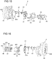
- the printed circuit board 41 has two first openings 410, through which contact elements 45 in the form of load contacts extend in such a way that the contact elements 45 with contact sections 450 in the form of socket sections (see 15 and 16 ) come to rest in the plug domes 401 of the plug face 400.
- a collar 452 protruding radially from a shaft section 451 of the respective contact element 42 comes to rest on a side of the printed circuit board 41 facing away from the plug domes 401, and a connection end 453 adjoining the collar 452 lies in the receiving space 404, so that the respective contact element 45 overlaps the connection end 453 can be connected to an associated load line.
- the printed circuit board 41 also has an opening 411, which is arranged centrally below the openings 410 and through which a contact element 46 in the form of a ground contact (so-called PE contact) engages in such a way that the contact element 46 fits into an associated plug dome 402 of the plug face 400 protrudes.
- a collar of the contact element 46 which is formed analogously to the collar 452, comes to rest on the side of the printed circuit board 41 facing away from the plug dome 402, so that the contact element 46 can be connected to an associated grounding line within the receiving space 404.
- Contact elements 42 in the form of signal contacts also lie in plug domes 403 above the plug domes 401 assigned to the contact elements 42 in the form of the load contacts and interact with the printed circuit board 41.
- Contact springs 412, 413, 415 for thermal and / or electrical contacting with the contact elements 42, 45, 46 are arranged on the printed circuit board 41.
- the contact springs 412, 413, 415 are designed, for example, as surface-mounted spring elements (for example SMD-soldered spring elements) and project axially from the printed circuit board 41 on different sides.
- Two first groups of contact springs 412 are grouped around the first openings 410 and are used to make thermal contact with a collar 452 on a shaft section 451 of an associated contact element 45 in the form of a load contact, so that the contact elements 45 are in shape via the contact springs 412 of the load contacts are thermally connected to the printed circuit board 41 and heat via the contact springs 412 towards the printed circuit board 41 and thus towards a temperature sensor 417 arranged on the printed circuit board 41 (see Fig. 13 ) can be directed. Temperature monitoring on the contact elements 45 in the form of the load contacts can thus be provided via the printed circuit board 41.
- the contact elements 45 in the form of the load contacts are arranged on a load contact carrier 44 and are mechanically fixed to the housing part 40 via the load contact carrier 44 and thus held in position with respect to the housing part 40.
- the contact elements 45 each engage with their collar 452 in an assigned semicircular receiving groove 441 on a receiving device 440 of the load contact carrier 44, so that the respective contact element 45 extends through the assigned opening 410 of the printed circuit board 41 and the connection end 453 facing away from the contact section 54 in the region of the Connection device 440 comes to rest.
- the contact springs 412 which are grouped around the opening 410 associated with a respective contact element 45, are located in a region outside the receiving groove 441, as viewed in the circumferential direction around the respective opening 410, or engage in a recess 442 in the region of the receiving groove 441 (please refer Fig. 16 ) to make thermal contact with the collar 452 of the respective contact element 45.
- Contact springs 413 are grouped around the opening 411 and are used to make electrical contact with a contact element 46 in the form of an earth contact.
- the contact element 46 extends through the opening 411, rests with its radially projecting collar on the associated contact springs 413 and is thus electrically connected to the printed circuit board 41.
- contact springs 415 are arranged which are assigned to the contact elements 42 in the form of the signal contacts and which are each arranged between a pair of through openings 414 through which a signal contact carrier 43 with fixing elements 431 extends ( please refer 9 and 11 together with 7 and 8 ).
- the signal contact carrier 43 is attached with a surface section 430 to the side of the printed circuit board 41 facing away from the signal contacts 42 and engages with the fixing elements 431 through the through openings 414 of the printed circuit board 41 in such a way that the fixing elements 431 axially position the contact elements 42 in the form of the signal contacts in the Plug domes 403 of the plug face 400 are held.
- the fixing elements 431 act on ends 421 of the contact elements 42 in the form of the signal contacts and thus lock them axially in the plug domes 43.
- the contact elements 42 in the form of the signal contacts are electrically connected to the printed circuit board 41 via the contact springs 415.
- Resistance coding is provided on the plug connector part 4 via the printed circuit board 41, in that an electrical resistance 416 (see. FIG Fig. 14 ) is connected between the contact elements 42, 46, for example between a contact element 42 forming a proximity contact and the contact element 46 in the form of the grounding contact.
- connection lines 420 can be connected to the printed circuit board 41, via which the contact elements 42 are electrically connected to a higher-level assembly, for example a higher-level control device (see Fig. 14 ). Connection lines 420 can thus be guided over the printed circuit board 41, which makes a direct connection of the connection lines 420 with the associated contact elements 42 superfluous and thus simplifies the assembly of the connector part 4.
- the signal contract carrier 43 is fixedly connected to the load contact carrier 44 and fixed to the housing part 40 via the load contact carrier 44.
- the signal contact carrier 43 reaches with its fixing elements 431 through the assigned passage openings 414 to act on the contact elements 42.
- the load contact carrier 44 with passage bars 443 passes through slot-shaped passage openings 418 associated with it, as is the case here Fig. 16 together for example with 11 and 14 can be seen.
- the circuit board 41 is in this way - at least during assembly - axially floating on the signal contact carrier 43 and the load contact carrier 44, the circuit board 41 being held in position in the housing part 40 elastically via the contact springs 412, 413, 415 on both sides of the circuit board 41 .
- the circuit board 41 together with the signal contact carrier 43 and the load contact carrier 44 is in the receiving space 404 of the Housing part 40 inserted such that the circuit board 41 with the contact springs 415 comes into contact with the ends 421 of the contact elements 42.
- the printed circuit board 41 thus assumes an intermediate layer between the contact elements 42 on the one hand and the contact elements 45, 46 on the other hand - with elastic prestressing of the contact springs 412, 413, 415, so that the printed circuit board 41 under elastic prestressing of the contact springs 412, 413, 415 is held axially in position. Due to the elasticity of the contact springs 412, 413, 415, tolerances in the material thickness of the circuit board 41 can be compensated, which makes the assembly of the connector part 4 insensitive to tolerances.
- the printed circuit board 41 is fixed within the receiving space 404 via fastening domes 405 arranged on the housing part 40 by caulking the fastening domes 405 and thereby fixing the printed circuit board 41 to the housing part 40.
- circuit board 41 extends perpendicular to the direction of extension of the contact elements 42, 45, 46, 47 in the receiving space 404 of the housing part 40, there is a space-efficient arrangement of the circuit board 41 in the housing part 40, with simple assembly of the connector part 4 and more reliable thermal and / or electrical contacting with the associated contact elements 42, 45, 46.
- the creation of a preassembled module is also made possible via the circuit board 41, in which connection lines 420 in particular can be preassembled on the circuit board 41. The need for a direct connection of connection lines 420 to associated contact elements 42, for example by crimping, is eliminated.
- a connector part of the type described here can advantageously be used in a charging system for charging an electric vehicle.
- the connector part can implement a charging socket (as in the exemplary embodiments shown) or a charging plug.
- a connector part of the type described can be used wherever temperature monitoring on contact elements is desirable.
Landscapes
- Engineering & Computer Science (AREA)
- Microelectronics & Electronic Packaging (AREA)
- Power Engineering (AREA)
- Transportation (AREA)
- Mechanical Engineering (AREA)
- Details Of Connecting Devices For Male And Female Coupling (AREA)
- Coupling Device And Connection With Printed Circuit (AREA)
Abstract
Description
- Die Erfindung betrifft ein Steckverbinderteil zum steckenden Verbinden mit einem Gegensteckverbinderteil nach dem Oberbegriff des Anspruchs 1.
- Ein derartiges Steckverbinderteil umfasst ein Gehäuseteil, ein an dem Gehäuseteil geformtes Steckgesicht, über das das Steckverbinderteil steckend mit dem Gegensteckverbinderteil verbindbar ist und an dem eine Mehrzahl von Kontaktelementen zum elektrischen Verbinden mit dem Gegensteckverbinderteil angeordnet ist, und eine Leiterplatte, an der zumindest eine elektrische oder elektronische Funktionskomponente angeordnet ist.
- Bei einem solchen Steckverbinderteil kann es sich beispielsweise um einen Stecker oder auch eine Buchse handeln. Ein solches Steckverbinderteil kann insbesondere an einer Ladeeinrichtung zum Übertragen eines Ladestroms zum Einsatz kommen. Das Steckverbinderteil kann insbesondere als Ladestecker oder Ladebuchse zum Laden eines elektromotorisch angetriebenen Kraftfahrzeugs (bezeichnet auch als Elektrofahrzeug) ausgebildet sein und kann auf Seiten einer Ladestation, z.B. als Ladestecker an einem Ladekabel, oder auch auf Seiten eines Fahrzeugs als sogenannter Inlet verwendet werden.
- Ladestecker oder Ladebuchsen zum Aufladen von Elektrofahrzeugen sind so auszulegen, dass große Ladeströme übertragen werden können. Weil die thermische Verlustleistung quadratisch mit dem Ladestrom wächst und zudem vorgeschrieben ist, dass eine Temperaturerhöhung an einem Steckverbinderteil 50 K nicht überschreiten darf, ist bei solchen Ladesteckern oder Ladebuchsen erforderlich, eine Temperaturüberwachung bereitzustellen, um eine Überhitzung an Bauteilen des Ladesteckers oder der Ladebuchse frühzeitig zu erkennen und gegebenenfalls eine Modifizierung des Ladestroms oder gar eine Abschaltung der Ladeeinrichtung zu bewirken. Beispielsweise sind bei einem aus der
DE 10 2015 106 251 A1 bekannten Steckverbinderteil Kontaktelemente beispielweise in Öffnungen einer Leiterplatte angeordnet. An der Leiterplatte sind ein oder mehrere Sensoreinrichtungen vorgesehen, die dazu dienen, eine Erwärmung an einem oder mehreren Kontaktelementen zu erfassen. - Um zudem sicherzustellen, dass bei Verbindung eines Elektrofahrzeugs mit einer Ladestation über ein Ladekabel ein in das Elektrofahrzeug eingespeister Ladestrom eine zulässige Maximalstromstärke, für die das Ladekabel und ein Ladesystem des Elektrofahrzeugs ausgelegt sind, nicht überschritten wird, wird an Steckverbinderteilen eine Widerstandskodierung verwendet, wie dies beispielsweise in der
DE 10 2010 053 074 A1 , derDE 20 2012 100 613 U1 und derDE 10 2013 110 548 A1 beschrieben und zudem in einschlägigen Normen, beispielsweise der IEC 62196, normiert ist. Beispielsweise kann in einem Stecker eines Ladekabels zwischen einem so genannten Näherungskontakt und einem Schutzleiterkontakt ein Widerstand geschaltet sein, dessen Widerstandswert bei Anschließen des Steckers an eine Ladestation über die Ladestation gemessen werden kann, um anhand des Widerstandswerts den Typ des angeschlossenen Ladekabels zu erkennen. Unterschiedlichen Widerstandswerten sind hierbei bestimmte Typen von Ladekabeln oder Ladeeinrichtungen zugeordnet, so dass anhand des Widerstandswerts dieser Typ identifiziert werden kann. Insbesondere kann auf diese Weise eine zulässige Maximalstromstärke, die beispielsweise über ein Ladekabel übertragen werden kann (beispielsweise 16 A oder 32 A) identifiziert werden, so dass entsprechend die Ladestation einen eingespeisten Strom begrenzen kann. Zu ähnlichem Zweck dient eine Widerstandskodierung beispielsweise an einem Steckverbinderteil in Form einer Ladebuchse an einem Elektrofahrzeug. In diesem Fall kann anhand eines Widerstandswerts insbesondere ein maximal zulässiger Ladestrom, für den das Ladesystem des Elektrofahrzeugs ausgelegt ist, identifiziert werden. - Um unterschiedliche elektrische und/oder elektronische Funktionen, zum Beispiel eine Temperarturüberwachung oder eine Widerstandkodierung, an einem Steckverbinderteil zur Verfügung zu stellen, ist herkömmlich bereits vorgesehen worden, eine Leiterplatte mit daran angeordneten Funktionskomponenten in einem Steckverbinderteil anzuordnen. Wünschenswert ist dabei eine platzeffiziente Anordnung der Leiterplatte in dem Steckverbinderteil bei zuverlässiger thermischer und/oder elektrischer Kontaktierung mit zugeordneten Kontaktelementen und einfacher Montage des Steckverbinderteils.
- Aufgabe der vorliegenden Erfindung ist es, ein Steckverbinderteil bereitzustellen, das eine platzsparende Anordnung einer Leiterplatte bei vorteilhafter thermischer und/oder elektrischer Kontaktierung mit zugeordneten Kontaktelementen und bei zudem einfacher Montage der Leiterplatte in dem Steckverbinderteil ermöglicht.
- Diese Aufgabe wird durch einen Gegenstand mit den Merkmalen des Anspruchs 1 gelöst.
- Demnach weist die Leiterplatte eine erste Öffnung auf, durch die ein erstes Kontaktelement der Mehrzahl von Kontaktelementen hindurch erstreckt ist, wobei die Leiterplatte zumindest eine erste Kontaktfeder zum thermischen und/oder elektrischen Kontaktieren mit dem ersten Kontaktelement oder zumindest eine zweite Kontaktfeder zum thermischen und/oder elektrische Kontaktieren mit einem zweiten Kontaktelement der Mehrzahl von Kontaktelementen aufweist.
- Die Leiterplatte dient dazu, an dem Steckverbinderteil elektrische und/oder elektronische Funktionen bereitzustellen. Insbesondere kann an Lastkontakten des Steckverbinderteils eine Temperaturüberwachung bereitgestellt werden. Zudem kann über die Leiterplatte beispielsweise eine Widerstandskodierung verwirklicht werden. Die Kontaktelemente des Steckverbinderteils erstrecken sich hierbei beispielsweise axial entlang einer Steckrichtung, entlang derer das Steckverbinderteil mit dem zugeordneten Gegensteckverbinderteil zu verbinden ist. Dadurch, dass ein erstes Kontaktelement eine Öffnung der Leiterplatte durchgreift, kann sich die Leiterplatte vorzugsweise näherungsweise senkrecht zu der Steckrichtung und somit senkrecht zur Längserstreckungsrichtung der Kontaktelemente erstrecken, was ermöglicht, die Leiterplatte bauraumeffizient in dem Gehäuseteil des Steckverbinderteils einzufassen.
- Über die an der Leiterplatte angeordneten Kontaktfedern wird eine zuverlässige, einfach herzustellende Kontaktierung zur thermischen und/oder elektrischen Kopplung der Kontaktelemente mit der Leiterplatte bereitgestellt. Bei der Montage des Steckverbinderteils gelangen die zugeordneten Kontaktelemente selbsttätig in Anlage mit zugeordneten Kontaktfedern der Leiterplatte, sodass dadurch eine thermische und/oder elektrische Ankopplung der Kontaktelemente an die Leiterplatte bereitgestellt wird, ohne dass weitere Maßnahmen zur Kopplung der Leiterplatte mit den Kontaktelementen ergriffen werden müssen. Die Kontaktfedern können beispielsweise als oberflächenmontierte (zum Beispiel SMD-gelötete) Federelemente ausgebildet sein, die bei der Montage des Steckverbinderteils selbsttätig unter elastischer Verspannung in Anlage mit den zugeordneten Kontaktelementen gelangen.
- Es ergibt sich eine einfache Montage bei bauraumeffizienter Aufnahme der Leiterplatte in dem Gehäuseteil des Steckverbinderteils und bei zudem zuverlässiger thermischer und/oder elektrischer Kontaktierung der Leiterplatte mit zugeordneten Kontaktelementen.
- In einer Ausgestaltung sind die zumindest eine erste Kontaktfeder und die zumindest eine zweite Kontaktfeder an unterschiedlichen Seiten der Leiterplatte angeordnet. An einer ersten Seite kann die Leiterplatte beispielsweise eine oder mehrere erste Kontaktfedern zur Kontaktierung mit dem zugeordneten ersten Kontaktelement, beispielsweise einem Lastkontakt, aufweisen. An einer der ersten Seite abgewandten, zweiten Seite weist die Leiterplatte demgegenüber eine oder mehrere zweite Kontaktfedern zur Kontaktierung mit dem zweiten Kontaktelement, beispielsweise einem Signalkontakt, auf. An der Leiterplatte können hierbei jeweils mehrere Gruppen von ersten Kontaktfedern und zweiten Kontaktfedern angeordnet sein, die zur Kontaktierung mit mehreren ersten Kontaktelementen, zum Beispiel mehreren Lastkontakten, und mehreren zweiten Kontaktelementen, zum Beispiel mehreren Signalkontakten, dienen. Die Kontaktfedern sind axial, also senkrecht zur Ebene der Leiterplatte, federnd und gelangen somit bei der Montage des Steckverbinderteils unter axialer Verspannung in Anlage mit den zugeordneten Kontaktelementen.
- In einer Ausgestaltung weist das erste Kontaktelement einen die erste Öffnung der Leiterplatte durchgreifenden Schaftabschnitt und einen an dem Schaftabschnitt angeordneten Bund auf. Der Bund steht radial von dem Schaftabschnitt vor und kontaktiert über die zumindest eine erste Kontaktfeder die Leiterplatte thermisch und/oder elektrisch derart, dass über den Bund eine thermische und/oder elektrische Kopplung des Kontaktelements mit der Leiterplatte hergestellt ist. An den Schaftabschnitt kann sich einerseits zum Beispiel ein Kontaktabschnitt, zum Beispiel in Form eines Buchsenabschnitts zum Verwirklichen einer Kontaktbuchse, zum elektrischen Kontaktieren mit einem zugeordneten Gegenkontaktelement eines Gegensteckverbinderteils anschließen, der in das Steckgesicht hineinragt. Andererseits kann an dem Schaftabschnitt ein Anschlussende angeordnet sein, über das eine Leitung an das Kontaktelement angeschlossen werden kann, beispielsweise eine Lastleitung zum Leiten eines Laststroms hin zu dem ersten Kontaktelement.
- Ist die zumindest eine erste Kontaktfeder mit dem Bund des ersten Kontaktelements in Anlage, so kann die Leiterplatte vorzugsweise axial zwischen dem Bund und dem zweiten Kontaktelement abgestützt und somit - zumindest bei der Montage - axial schwimmend in Position gehalten werden. Über die zumindest eine zweite Kontaktfeder ist die Leiterplatte elastisch federnd zum Beispiel zu einem Ende des zweiten Kontaktelements abgestützt. Die Leiterplatte wird somit in elastischer Weise zwischen dem Bund des ersten Kontaktelements und dem zweiten Kontaktelement gehalten, was die Montage der Leiterplatte in dem Gehäuseteil des Steckverbinderteils unempfindlich gegenüber Toleranzen macht und zum Beispiel das Verwenden von Leiterplatten unterschiedliche Stärke ohne bauliche Anpassung anderer Baugruppen des Steckverbinderteils ermöglicht.
- Nach dem Anordnen an dem Gehäuseteil (und einem zunächst schwimmenden axialen Halt) ist hierbei möglich, die Leiterplatte axial zu dem Gehäuseteil festzulegen, beispielsweise durch Verstemmen von an der Leiterplatte oder dem Gehäuseteil angeordneten Befestigungsdomen.
- Das erste Kontaktelement kann beispielsweise einen Lastkontakt zum Betreiben eines Laststroms, zum Beispiel eines Ladestroms zum Aufladen eines Elektrofahrzeugs, verwirklichen. Weil es an einem solchen Lastkontakt im Betrieb des Steckverbinderteils zu einer Erwärmung kommen kann, ist an dem ersten Kontaktelement vorzugsweise eine Temperaturüberwachung vorgesehen, die dadurch ermöglicht wird, dass das erste Kontaktelement über die zumindest eine erste Kontaktfeder thermisch mit der Leiterplatte verbunden ist, sodass Wärme von dem ersten Kontaktelement hin zu der Leiterplatte und hin zu einem an der Leiterplatte angeordneten Temperatursensor geleitet werden kann, um über den Temperatursensor eine Erwärmung an dem ersten Kontaktelement zu erfassen.
- Die Leiterplatte kann beispielsweise eine Steuereinrichtung aufweisen, der Sensorsignale des Temperatursensors zugeleitet werden, wobei die Steuereinrichtung ausgebildet sein kann, die Sensorsignale auszuwerten und gegebenenfalls geeignete Gegenmaßnahmen einzuleiten (zum Beispiel einen Ladevorgang zu unterbrechen), wenn eine (übermäßige) Erwärmung an dem ersten Kontaktelement erkannt wird.
- Ein solcher Temperatursensor kann beispielsweise durch einen temperaturabhängigen Widerstand ausgebildet sein. Bei einem solchen Temperatursensor kann es sich beispielsweise um einen Widerstand mit einem positiven Temperaturkoeffizienten (sogenannte PTC-Widerstand) handeln, dessen Widerstandswert mit steigender Temperatur ansteigt (auch bezeichnet als Kaltleiter, der bei niedriger Temperatur eine gute elektrische Leitfähigkeit und bei höheren Temperaturen eine reduzierte elektrische Leitfähigkeit aufweist). Solch ein Temperatursensor kann beispielsweise auch eine nichtlineare Temperaturkennlinie aufweisen und kann beispielsweise aus einem Keramikmaterial hergestellt sein (sogenannter Keramik-Kaltleiter).
- Es kann alternativ beispielsweise aber auch ein elektrischer Widerstand mit negativem Temperaturkoeffizienten (sogenannte NTC-Widerstände) als Temperatursensor zum Einsatz kommen, dessen Widerstandswert mit steigender Temperatur sinkt.
- Alternativ oder zusätzlich kann auch ein durch ein Halbleiterbauelement ausgebildeter Temperatursensor zum Einsatz kommen.
- In einer Ausgestaltung verwirklicht das zweite Kontaktelement einen Signalkontakt zum Übertragen oder Erfassen von Steuersignalen. Bei einem Steckverbinderteil im Rahmen eines Ladesystems zum Aufladen eines Elektrofahrzeugs können über solche Signalkontakte beispielsweise Steuersignale übertragen werden, die einen Ladevorgang steuern und über die zum Beispiel Kontrollsignale zwischen einem Fahrzeug und einer Ladestation ausgetauscht werden. Über einen solchen Signalkontakt werden somit elektrische Signale niedriger Spannung und niedriger Stromstärke zum Austausch von Informationen und Steuerkommandos übertragen. Über die zumindest eine zweite Kontaktfeder kann insbesondere eine elektrische Ankopplung erfolgen, beispielsweise um eine Widerstandskodierung bereitzustellen. Über eine solche Widerstandskodierung kann beispielsweise anhand des Widerstandswertes eines elektrischen Widerstands der Typ eines angeschlossenen Ladekabels oder einer Ladestation oder eine zulässige Maximalstromstärke identifiziert werden.
- Zusätzlich oder alternativ kann über die zumindest eine zweite Kontaktfeder auch eine Anschlussleitung mit dem zweiten Kontaktelement verbunden sein. Der Anschlussleitung ist in diesem Fall an die Leiterplatte angeschlossen und elektrisch über die zumindest eine zweite Kontaktfeder mit dem zweiten Kontaktelement gekoppelt. Eine direkte Verbindung der Anschlussleitung mit dem zweiten Kontaktelement zum Beispiel durch Vercrimpen ist in diesem Fall nicht erforderlich, was die Montage des Steckverbinderteils erheblich vereinfacht.
- Generell können für solche Kontaktelemente des Steckverbinderteils, die keine Lastströme übertragen, Anschlussleitungen über die Leiterplatte geführt werden, was ermöglicht, eine vormontierte Baueinheit zu schaffen, im Rahmen derer Anschlussleitungen an die Leiterplatte angeschlossen sind und eine Kopplung mit zugeordneten Kontaktelementen dann über Kontaktfedern an der Leiterplatte erfolgt. Dies kann die Herstellung des Steckverbinderteils wesentlich vereinfachen.
- In einer Ausgestaltung weist die Leiterplatte eine zweite Öffnung auf, durch die ein drittes Kontaktelement hindurch erstreckt ist, wobei die Leiterplatte zumindest eine dritte Kontaktfeder zum thermischen und/oder elektrischen Kontaktieren mit dem dritten Kontaktelement aufweist. Bei dem dritten Kontaktelement kann es sich beispielsweise um einen Erdungskontakt (so genannter PE-Kontakt) handeln, über den eine Erdung an dem Steckverbinderteil zur Verfügung gestellt wird. Über eine oder mehrere dritte Kontaktfedern kann das dritte Kontaktelement hierbei insbesondere elektrisch mit der Leiterplatte verbunden sein, wobei das dritte Kontaktelement über die Leiterplatte und einen an der Leiterplatte angeordneten elektrischen Widerstand mit dem zweiten Kontaktelement verbunden ist, um auf diese Weise durch einen zwischen das dritte Kontaktelement und das zweite Kontaktelement geschalteten elektrischen Widerstand eine Widerstandskodierung an dem Steckverbinderteil zur Verfügung zu stellen.
- Das Steckverbinderteil weist, in einer Ausgestaltung, einen Signalkontaktträger auf, der die Leiterplatte zur Fixierung des zweiten Kontaktelements an dem Gehäuseteil an einer ersten Durchflussöffnung durchgreift. Der Signalkontaktträger dient insbesondere dazu, das zweite Kontaktelement, das beispielsweise einen Signalkontakt verwirklicht, axial in Position an dem Gehäuseteil zu halten, sodass das zweite Kontaktelement positionsfest an dem Steckgesicht fixiert ist. Der Signalkontraktträger kann hierzu beispielsweise an eine dem zweiten Kontaktelement abgewandten Seite der Leiterplatte angesetzt sein und durchgreift mit einem Fixierelement eine zugeordnete Durchgriffsöffnung an der Leiterplatte, um über das Fixierelement auf das zweite Kontaktelement einzuwirken und dieses zu fixieren. Der Signalkontaktträger ist zum Beispiel über eine andere Gehäusebaugruppe mit dem Gehäuseteil verbunden und zu dem Gehäuseteil festgelegt, sodass über den Signalkontaktträger ein oder mehrere zweite Kontaktelemente zu dem Gehäuseteil fixiert sind.
- In einer Ausgestaltung weist das Steckverbinderteil zudem einen mit dem Gehäuseteil verbundenen Lastkontaktträger auf, an dem ein oder mehrere erste Kontaktelemente, insbesondere in Form von Lastkontakten, angeordnet sind. Der Lastkontaktträger kann hierbei die ersten Kontaktelemente in Form der Lastkontakte mechanisch fixieren und somit zu den Gehäuseteil festlegen, wobei der Lastkontaktträger beispielsweise durch die Leiterplatte hindurch greift und somit die Leiterplatte lagert.
- Das Steckverbinderteil kann beispielsweise als Ladestecker oder als Ladebuchse eines Ladesystems zum Aufladen eines Elektrofahrzeugs Verwendung finden. Das Steckverbinderteil weist hierzu Kontaktelemente auf, die als Lastkontakte zum Übertragen eines Ladestroms zum Beispiel in Form eines Gleichstroms oder in Form eines Wechselstroms dienen.
- Der der Erfindung zugrunde liegende Gedanke soll nachfolgend anhand der in den Figuren dargestellten Ausführungsbeispiele näher erläutert werden. Es zeigen:
- Fig.1
- eine schematische Darstellung eines Elektrofahrzeugs mit einem Ladekabel und einer Ladestation zum Aufladen;
- Fig. 2
- eine Ansicht eines Steckverbinderteils in Form eines Inlets auf Seiten eines Fahrzeugs;
- Fig. 3
- eine rückseitige Ansicht des Steckverbinderteils;
- Fig. 4
- eine Seitenansicht des Steckverbinderteils;
- Fig. 5
- eine Draufsicht auf der Steckverbinderteil;
- Fig. 6
- eine Ansicht des Steckverbinderteils schräg von hinten;
- Fig. 7
- eine Teilexplosionsansicht des Steckverbinderteils, schräg von vorne;
- Fig. 8
- eine Teilexplosionsansicht des Steckverbinderteils, schräg von hinten;
- Fig. 9
- eine Vorderansicht einer in einem Gehäuseteil des Steckverbinderteils aufgenommenen Leiterplatte;
- Fig. 10
- eine Seitenansicht der Leiterplatte;
- Fig. 11
- eine rückwärtige Ansicht der Leiterplatte;
- Fig. 12
- eine Draufsicht auf die Leiterplatte;
- Fig. 13
- eine Ansicht der Leiterplatte schräg von vorne;
- Fig. 14
- eine Ansicht der Leiterplatte, schräg von hinten;
- Fig. 15
- eine Explosionsansicht des Steckverbinderteils; und
- Fig. 16
- eine Explosionsansicht des Steckverbinderteils, schräg von vorne.
-
Fig. 1 zeigt in einer schematischen Ansicht ein Fahrzeug 1 in Form eines elektromotorisch angetriebenen Fahrzeugs (bezeichnet auch als Elektrofahrzeug). Das Elektrofahrzeug 1 verfügt über elektrisch aufladbare Batterien, über die ein Elektromotor zum Fortbewegen des Fahrzeugs 1 elektrisch versorgt werden kann. - Um die Batterien des Fahrzeugs 1 aufzuladen, kann das Fahrzeug 1 über ein Ladekabel 3 an eine Ladestation 2 angeschlossen werden. Das Ladekabel 3 kann hierzu mit einem Ladestecker 30 an einem Ende in ein zugeordnetes Steckverbinderteil 4 in Form einer Ladebuchse des Fahrzeugs 1 eingesteckt werden und steht an seinem anderen Ende über einen anderen Ladestecker 31 mit einem Steckverbinderteil 4 in Form einer Ladebuchse an der Ladestation 2 in elektrischer Verbindung. Über das Ladekabel 3 werden Ladeströme mit vergleichsweise großer Stromstärke hin zum Fahrzeug 1 übertragen.
-
Fig. 2 bis 16 zeigen ein Ausführungsbeispiel eines Steckverbinderteils 4 in Form einer Ladebuchse zum Beispiel auf Seiten eines Fahrzeugs (auch bezeichnet als Fahrzeuginlet), das steckend mit einem zugeordneten Gegensteckverbinderteil 30 in Form eines Ladesteckers an einem Ladekabel 3 verbunden werden kann, um das Elektrofahrzeug 1 mit der Ladestation 2 des Ladesystems zu verbinden. Das Steckverbinderteil 4 weist ein Gehäuseteil 40 auf, an dem ein Steckgesicht 400 geformt ist, mit dem das Gegensteckverbinderteil 30 entlang einer Steckrichtung E steckend verbunden werden kann. - Das Steckgesicht 400 wird gebildet durch Steckdome 401, 402, 403, in denen Kontaktelemente 42, 45, 46, 47 angeordnet sind und über die das Steckverbinderteil 4 entlang der Steckrichtung E steckend mit einem zugeordneten Gegensteckverbinderteil 30 verbunden werden kann. In einem verbundenen Zustand ist über die Steckdome 401, 402, 403 des Steckgesichts 400 eine mechanisch steckende Verbindung mit dem Gegensteckverbinderteil 30 hergestellt, unter elektrischer Kontaktierung der Kontaktelemente 42, 45, 46, 47 mit zugeordneten Gegenkontaktelementen des Gegensteckverbinderteils 30.
- Das Steckgesicht 400 ist an einer Vorderseite des Gehäuseteils 40 geformt. An einer dem Steckgesicht 400 abgewandten Rückseite weist das Gehäuseteil 40 einen Aufnahmeraum 404 (siehe zum Beispiel
Fig. 6 ) auf, in dem eine Leiterplatte 41 mit daran angeordneten elektrischen und/oder elektronischen Funktionskomponenten aufgenommen ist und über den elektrische Kontaktelemente 42, 45, 46, 47 in den Steckdomen 401, 402, 403 des Steckgesichts 400 angeordnet sind. - Die Leiterplatte 41 erstreckt sich entlang einer senkrecht zur Steckrichtung E gerichteten Ebene innerhalb des Aufnahmeraums 404. Die Leiterplatte 41 ist somit senkrecht zur Längserstreckungsrichtung der Kontaktelemente 42, 45, 46, 47 ausgerichtet, sodass die Leiterplatte 41 platzeffizient in dem Aufnahmeraum 404 des Gehäuseteils 40 aufgenommen ist.
- Die Leiterplatte 41 weist zwei erste Öffnungen 410 auf, durch die Kontaktelemente 45 in Form von Lastkontakten hindurch greifen derart, dass die Kontaktelemente 45 mit Kontaktabschnitten 450 in Form von Buchsenabschnitten (siehe
Fig. 15 und 16 ) in den Steckdomen 401 des Steckgesichts 400 zu liegen kommen. Ein radial von einem Schaftabschnitt 451 des jeweiligen Kontaktelements 42 vorstehender Bund 452 kommt hierbei an einer den Steckdomen 401 abgewandten Seite der Leiterplatte 41 zu liegen, und ein an den Bund 452 anschließendes Anschlussende 453 liegt in dem Aufnahmeraum 404 ein, sodass das jeweilige Kontaktelement 45 über das Anschlussende 453 mit einer zugeordneten Lastleitung verbunden werden kann. - Die Leiterplatte 41 weist zudem eine Öffnung 411 auf, die mittig unterhalb der Öffnungen 410 angeordnet ist und durch die ein Kontaktelement 46 in Form eines Erdungskontakts (so genannter PE-Kontakt) hindurch greift derart, dass das Kontaktelement 46 in einen zugeordneten Steckdom 402 des Steckgesichts 400 hineinragt. Ein - analog dem Bund 452 ausgebildeter - Bund des Kontaktelements 46 kommt an der dem Steckdom 402 abgewandten Seite der Leiterplatte 41 zu liegen, sodass das Kontaktelement 46 innerhalb des Aufnahmeraums 404 an eine zugeordnete Erdungsleitung angeschlossen sein kann.
- Kontaktelemente 42 in Form von Signalkontakten liegen zudem in Steckdomen 403 oberhalb der den Kontaktelementen 42 in Form der Lastkontakte zugeordneten Steckdome 401 ein und wirken mit der Leiterplatte 41 zusammen.
- An der Leiterplatte 41 sind Kontaktfedern 412, 413, 415 zur thermischen und/oder elektrischen Kontaktierung mit den Kontaktelementen 42, 45, 46 angeordnet. Die Kontaktfedern 412, 413, 415 sind zum Beispiel als oberflächenmontierte Federelemente (zum Beispiel SMD-gelötete Federelemente) ausgebildet und stehen axial zu unterschiedlichen Seiten von der Leiterplatte 41 vor.
- So sind zwei erste Gruppen von Kontaktfedern 412 um die ersten Öffnungen 410 herum gruppiert und dienen dazu, thermisch mit einem Bund 452 an einem Schaftabschnitt 451 eines jeweils zugeordneten Kontaktelements 45 in Form eines Lastkontakts zu kontaktieren, sodass über die Kontaktfedern 412 die Kontaktelemente 45 in Form der Lastkontakte thermisch an die Leiterplatte 41 angebunden sind und Wärme über die Kontaktfedern 412 hin zu der Leiterplatte 41 und somit hin zu einem an der Leiterplatte 41 angeordneten Temperatursensor 417 (siehe
Fig. 13 ) geleitet werden kann. Über die Leiterplatte 41 kann somit eine Temperarturüberwachung an den Kontaktelementen 45 in Form der Lastkontakte bereitgestellt werden. - Die Kontaktelemente 45 in Form der Lastkontakte sind an einem Lastkontaktträger 44 angeordnet und werden über den Lastkontaktträger 44 mechanisch zu dem Gehäuseteil 40 festgelegt und somit in Position zu dem Gehäuseteil 40 gehalten. Die Kontaktelemente 45 greifen jeweils mit ihrem Bund 452 in eine zugeordnete halbkreisförmige Aufnahmenut 441 an einer Aufnahmeeinrichtung 440 des Lastkontaktträgers 44 ein, sodass das jeweilige Kontaktelement 45 durch die zugeordnete Öffnung 410 der Leiterplatte 41 hindurch greift und das dem Kontaktabschnitt 54 abgewandte Anschlussende 453 im Bereich der Anschlusseinrichtung 440 zu liegen kommt. Die Kontaktfedern 412, die um die einem jeweiligen Kontaktelement 45 zugeordnete Öffnung 410 herum gruppiert sind, befinden sich hierbei - betrachtet in Umfangsrichtung um die jeweilige Öffnung 410 - in einem Bereich außerhalb der Aufnahmenut 441 oder greifen in eine Aussparung 442 im Bereich der Aufnahmenut 441 ein (siehe
Fig. 16 ), um thermisch mit dem Bund 452 des jeweiligen Kontaktelements 45 zu kontaktieren. - Um die Öffnung 411 herum sind Kontaktfedern 413 gruppiert, die zur elektrischen Kontaktierung mit einem Kontaktelement 46 in Form eines Erdungskontakts dienen. Das Kontaktelement 46 erstreckt sich durch die Öffnung 411 hindurch, liegt mit seinem radial vorstehenden Bund an den zugeordneten Kontaktfedern 413 an und ist somit elektrisch an die Leiterplatte 41 angeschlossen.
- An einer den Kontaktfedern 412, 413 abgewandten Seite der Leiterplatte 41 sind Kontaktfedern 415 angeordnet, die den Kontaktelementen 42 in Form der Signalkontakte zugeordnet sind und die jeweils zwischen einem Paar von Durchgriffsöffnungen 414 angeordnet sind, durch die ein Signalkontaktträger 43 mit Fixierelementen 431 hindurch greift (siehe
Fig. 9 und 11 in Zusammenschau mitFig. 7 und 8 ). Der Signalkontaktträger 43 ist mit einem Flächenabschnitt 430 an die den Signalkontakten 42 abgewandte Seite der Leiterplatte 41 angesetzt und greift mit den Fixierelementen 431 durch die Durchgriffsöffnungen 414 der Leiterplatte 41 hindurch derart, dass über die Fixierelemente 431 die Kontaktelemente 42 in Form der Signalkontakte axial in Position in den Steckdomen 403 des Steckgesichts 400 gehalten werden. Die Fixierelemente 431 wirken hierzu auf Enden 421 der Kontaktelemente 42 in Form der Signalkontakte ein und sperren diese somit axial in den Steckdomen 43. - Über die Kontaktfedern 415 sind die Kontaktelemente 42 in Form der Signalkontakte elektrisch an die Leiterplatte 41 angebunden. Über die Leiterplatte 41 wird eine Widerstandskodierung an dem Steckverbinderteil 4 bereitgestellt, indem über die elektrische Kontaktierung eines der Kontaktelemente 42 in Form der Signalkontakte und des Kontaktelements 46 in Form des Erdungskontakts ein elektrischer Widerstand 416 (siehe
Fig. 14 ) zwischen die Kontaktelemente 42, 46 geschaltet wird, zum Beispiel zwischen ein einen Näherungskontakt ausbildendes Kontaktelement 42 und das Kontaktelement 46 in Form des Erdungskontakts. - Zudem können an die Leiterplatte 41 Anschlussleitungen 420 angeschlossen sein, über die die Kontaktelemente 42 elektrisch mit einer übergeordneten Baugruppe, zum Beispiel einer übergeordneten Steuereinrichtung, verbunden sind (siehe
Fig. 14 ). Anschlussleitungen 420 können somit über die Leiterplatte 41 geführt werden, was ein direktes Verbinden der Anschlussleitungen 420 mit den zugeordneten Kontaktelementen 42 überflüssig macht und somit die Montage des Steckverbinderteils 4 vereinfacht. - Der Signalkontraktträger 43 ist fest mit dem Lastkontaktträger 44 verbunden und über den Lastkontaktträger 44 zu dem Gehäuseteil 40 festgelegt. Der Signalkontaktträger 43 greift, wie beschrieben, mit seinen Fixierelementen 431 durch die zugeordneten Durchgriffsöffnungen 414 zum Einwirken auf die Kontaktelemente 42. Zudem durchgreift der Lastkontaktträger 44 mit Durchgriffsstegen 443 zugeordnete schlitzförmige Durchgriffsöffnungen 418, wie dies aus
Fig. 16 in Zusammenschau zum Beispiel mitFig. 11 und 14 ersichtlich ist. Die Leiterplatte 41 ist auf diese Weise - zumindest während der Montage - axial schwimmend an dem Signalkontaktträger 43 und dem Lastkontaktträger 44 gelagert, wobei die Leiterplatte 41 elastisch über die Kontaktfedern 412, 413, 415 beidseits der Leiterplatte 41 in Position in dem Gehäuseteil 40 gehalten wird. - Zur Montage des Steckverbinderteils 4 wird die Leiterplatte 41 zusammen mit dem Signalkontaktträger 43 und dem Lastkontaktträger 44 in den Aufnahmeraum 404 des Gehäuseteils 40 eingesetzt derart, dass die Leiterplatte 41 mit den Kontaktfedern 415 in Anlage mit den Enden 421 der Kontaktelemente 42 gelangt. Bei der Montage nimmt die Leiterplatte 41 somit - unter elastischer Vorspannung der Kontaktfedern 412, 413, 415 - eine Zwischenlage zwischen den Kontaktelementen 42 einerseits und den Kontaktelementen 45, 46 andererseits ein, sodass die Leiterplatte 41 unter elastischer Vorspannung der Kontaktfedern 412, 413, 415 axial in Position gehalten ist. Aufgrund der Elastizität der Kontaktfedern 412, 413, 415 können Toleranzen in der Materialstärke der Leiterplatte 41 ausgeglichen werden, was die Montage des Steckverbinderteils 4 unempfindlich gegenüber Toleranzen macht.
- Nach der Montage wird die Leiterplatte 41 über an dem Gehäuseteil 40 angeordneten Befestigungsdomen 405 innerhalb des Aufnahmeraums 404 festgelegt, indem die Befestigungsdome 405 verstemmt werden und die Leiterplatte 41 dadurch zu dem Gehäuseteil 40 festgelegt wird.
- Weil die Leiterplatte 41 sich senkrecht zur Erstreckungsrichtung der Kontaktelemente 42, 45, 46, 47 in dem Aufnahmeraum 404 des Gehäuseteils 40 erstreckt, ergibt sich eine bauraumeffiziente Anordnung der Leiterplatte 41 in dem Gehäuseteil 40, bei zudem einfacher Montage des Steckverbinderteils 4 und zuverlässiger thermischer und/oder elektrischer Kontaktierung mit den zugeordneten Kontaktelementen 42, 45, 46. Insbesondere wird über die Leiterplatte 41 auch das Schaffen einer vormontierten Baugruppe ermöglicht, im Rahmen derer insbesondere Anschlussleitungen 420 an der Leiterplatte 41 vormontiert sein können. Das Erfordernis für ein direktes Anschließen von Anschlussleitungen 420 an zugeordnete Kontaktelemente 42, zum Beispiel durch Vercrimpen, entfällt.
- Der der Erfindung zugrunde liegende Gedanke ist nicht auf die vorangehend geschilderten Ausführungsbeispiele beschränkt, sondern lässt sich grundsätzlich auch in gänzlich andersgearteter Weise verwirklichen.
- Ein Steckverbinderteil der hier beschriebenen Art kann vorteilhaft in einem Ladesystem zum Aufladen eines Elektrofahrzeugs verwendet werden. Das Steckverbinderteil kann hierbei eine Ladebuchse (wie bei den dargestellten Ausführungsbeispielen) oder auch einen Ladestecker verwirklichen.
- Denkbar ist aber auch eine andere Verwendung. Grundsätzlich ist ein Steckverbinderteil der beschriebenen Art überall dort einsetzen, wo eine Temperaturüberwachung an Kontaktelementen wünschenswert ist.
-
- 1
- Fahrzeug
- 2
- Ladestation
- 3
- Ladekabel
- 30, 31
- Ladestecker
- 4
- Steckverbinderteil
- 40
- Gehäuseteil
- 400
- Steckgesicht
- 401-403
- Steckdome
- 404
- Aufnahmeraum
- 405
- Befestigungsdome
- 41
- Leiterplatte
- 410, 411
- Öffnung
- 412, 413
- Kontaktfeder
- 414
- Durchgriffsöffnung
- 415
- Kontaktfeder
- 416
- Widerstand
- 417
- Temperatursensor
- 418
- Durchgriffsöffnung
- 42
- Signalkontakte
- 420
- Anschlussleitung
- 421
- Ende
- 43
- Signalkontaktträger
- 430
- Flächenabschnitt
- 431
- Fixierelemente
- 44
- Lastkontaktträger
- 440
- Aufnahmeeinrichtung
- 441
- Aufnahmenut
- 442
- Aussparung
- 443
- Durchgriffssteg
- 45
- Lastkontakte
- 450
- Buchsenabschnitt
- 451
- Schaftabschnitt
- 452
- Bund
- 453
- Anschlussende
- 46
- Erdungskontakt (PE-Kontakt)
- 47
- Signalkontakt
- E
- Steckrichtung
Claims (15)
- Steckverbinderteil (4) zum steckenden Verbinden mit einem zugeordneten Gegensteckverbinderteil (30, 31), mit einem Gehäuseteil (40), einem an dem Gehäuseteil (40) geformten Steckgesicht (400), über das das Steckverbinderteil (4) steckend mit dem Gegensteckverbinderteil (30, 31) verbindbar ist und an dem eine Mehrzahl von Kontaktelementen (42, 45, 46, 47) zum elektrischen Verbinden mit dem Gegensteckverbinderteil (30, 31) angeordnet ist, und mit einer Leiterplatte (41), an der zumindest eine elektrische oder elektronische Funktionskomponente (416, 417) angeordnet ist, dadurch gekennzeichnet, dass die Leiterplatte (41) eine erste Öffnung (410) aufweist, durch die ein erstes Kontaktelement (45) der Mehrzahl von Kontaktelementen (42, 45, 46, 47) hindurch erstreckt ist, wobei die Leiterplatte (41) zumindest eine erste Kontaktfeder (412) zum thermischen und/oder elektrischen Kontaktieren mit dem ersten Kontaktelement (45) und zumindest eine zweite Kontaktfeder (415) zum thermischen und/oder elektrischen Kontaktieren mit einem zweiten Kontaktelement (42) der Mehrzahl von Kontaktelementen (42, 45, 46, 47) aufweist.
- Steckverbinderteil (4) nach Anspruch 1, dadurch gekennzeichnet, dass die zumindest eine erste Kontaktfeder (412) und die zumindest eine zweite Kontaktfeder (415) an unterschiedlichen Seiten der Leiterplatte (41) angeordnet sind.
- Steckverbinderteil (4) nach Anspruch 1 oder 2, dadurch gekennzeichnet, dass das erste Kontaktelement (45) einen die erste Öffnung (410) der Leiterplatte (41) durchgreifenden Schaftabschnitt (451) und einen an dem Schaftabschnitt (451) angeordneten Bund (452) aufweist, wobei die zumindest eine erste Kontaktfeder (415) den Bund (452) des ersten Kontaktelements (45) thermisch und/oder elektrisch kontaktiert.
- Steckverbinderteil (4) nach Anspruch 3, dadurch gekennzeichnet, dass die Leiterplatte (41) über die zumindest eine erste Kontaktfeder (412) und die zumindest eine zweite Kontaktfeder (415) zwischen dem Bund (452) des ersten Kontaktelements (45) und einem Ende (421) des zweiten Kontaktelements (42) elastisch federnd in Position gehalten ist.
- Steckverbinderteil (4) nach einem der vorangehenden Ansprüche, dadurch gekennzeichnet, dass das erste Kontaktelement (45) einen Lastkontakt zum Übertragen eines Laststroms verwirklicht.
- Steckverbinderteil (4) nach einem der vorangehenden Ansprüche, dadurch gekennzeichnet, dass die zumindest eine erste Kontaktfeder (412) das erste Kontaktelement (45) thermisch mit der Leiterplatte (41) verbindet, wobei die Leiterplatte (41) einen Temperatursensor (417) zum Erfassen einer Erwärmung an dem ersten Kontaktelement (45) aufweist.
- Steckverbinderteil (4) nach einem der vorangehenden Ansprüche, dadurch gekennzeichnet, dass das zweite Kontaktelement (42) einen Signalkontakt zum Übertragen von Steuersignalen verwirklicht.
- Steckverbinderteil (4) nach einem der vorangehenden Ansprüche, dadurch gekennzeichnet, dass die zumindest eine zweite Kontaktfeder (415) das zweite Kontaktelement (42) elektrisch mit der Leiterplatte (41) verbindet, wobei die Leiterplatte (41) einen elektrischen Widerstand (416) zum Bereitstellen einer Widerstandskodierung aufweist.
- Steckverbinderteil (4) nach einem der vorangehenden Ansprüche, dadurch gekennzeichnet, dass die zumindest eine zweite Kontaktfeder (415) das zweite Kontaktelement (42) elektrisch mit der Leiterplatte (41) verbindet, wobei zumindest eine Anschlussleitung (420) an die Leiterplatte (41) angeschlossen und elektrisch über die zumindest eine zweite Kontaktfeder (415) mit dem zweiten Kontaktelement (42) verbunden ist.
- Steckverbinderteil (4) nach einem der vorangehenden Ansprüche, dadurch gekennzeichnet, dass die Leiterplatte (41) eine zweite Öffnung (411) aufweist, durch die ein drittes Kontaktelement (46) hindurch erstreckt ist, wobei die Leiterplatte (41) zumindest eine dritte Kontaktfeder (413) zum thermischen und/oder elektrischen Kontaktieren mit dem dritten Kontaktelement (46) aufweist.
- Steckverbinderteil (4) nach Anspruch 10, dadurch gekennzeichnet, dass das dritte Kontaktelement (46) einen Erdungskontakt verwirklicht.
- Steckverbinderteil (4) nach Anspruch 10 oder 11, dadurch gekennzeichnet, dass die zumindest eine dritte Kontaktfeder (413) das dritte Kontaktelement (46) elektrisch mit der Leiterplatte (41) verbindet, wobei die Leiterplatte (41) das zweite Kontaktelement (42) und das dritte Kontaktelement (46) zur Bereitstellung einer Widerstandskodierung über einen elektrischen Widerstand (416) miteinander verbindet.
- Steckverbinderteil (4) nach einem der vorangehenden Ansprüche, gekennzeichnet durch einen Signalkontaktträger (43), der die Leiterplatte (41) zur Fixierung des zweiten Kontaktelements (42) an dem Gehäuseteil (40) an einer ersten Durchgriffsöffnung (414) durchgreift.
- Steckverbinderteil (4) nach einem der vorangehenden Ansprüche, gekennzeichnet durch einen mit dem Gehäuseteil (40) verbundenen Lastkontaktträger (44), an dem das erste Kontaktelement (45) angeordnet ist.
- Steckverbinderteil (4) nach Anspruch 14, dadurch gekennzeichnet, dass der Lastkontaktträger (44) die Leiterplatte (41) an einer zweiten Durchgriffsöffnung (418) durchgreift.
Applications Claiming Priority (1)
| Application Number | Priority Date | Filing Date | Title |
|---|---|---|---|
| BE20185869A BE1026857B1 (de) | 2018-12-10 | 2018-12-10 | Steckverbinderteil mit einer Leiterplatte |
Publications (2)
| Publication Number | Publication Date |
|---|---|
| EP3667831A1 true EP3667831A1 (de) | 2020-06-17 |
| EP3667831B1 EP3667831B1 (de) | 2022-04-27 |
Family
ID=65013410
Family Applications (1)
| Application Number | Title | Priority Date | Filing Date |
|---|---|---|---|
| EP19209323.5A Active EP3667831B1 (de) | 2018-12-10 | 2019-11-15 | Steckverbinderteil mit einer leiterplatte |
Country Status (4)
| Country | Link |
|---|---|
| US (1) | US11069992B2 (de) |
| EP (1) | EP3667831B1 (de) |
| JP (1) | JP6947800B2 (de) |
| BE (1) | BE1026857B1 (de) |
Cited By (4)
| Publication number | Priority date | Publication date | Assignee | Title |
|---|---|---|---|---|
| CN111806265A (zh) * | 2020-09-11 | 2020-10-23 | 潍坊美好生活环保科技有限公司 | 电动推送式充电桩及推送方法 |
| EP3958411A1 (de) * | 2020-08-21 | 2022-02-23 | Aptiv Technologies Limited | Elektrofahrzeugladeverbinder |
| EP4210176A1 (de) * | 2022-01-10 | 2023-07-12 | HARTING Automotive GmbH | Verfahren zur herstellung eines inlets, inlet und multikontaktstecker |
| EP4296112A1 (de) * | 2022-06-24 | 2023-12-27 | Hager Controls | Schnellverbindungsvorrichtung für ladeanschluss von elektrofahrzeugen und ladeanschluss für elektrofahrzeuge mit mindestens einer solchen vorrichtung |
Families Citing this family (11)
| Publication number | Priority date | Publication date | Assignee | Title |
|---|---|---|---|---|
| DE102017222541A1 (de) * | 2017-12-13 | 2019-06-13 | Bayerische Motoren Werke Aktiengesellschaft | Hochvolt-Steckverbindungsteil für einen Hochvolt-Steckverbinder eines Kraftfahrzeugs, Hochvoltbordnetz sowie Kraftfahrzeug |
| EP3751296A1 (de) * | 2019-06-12 | 2020-12-16 | LEM International SA | Gleichstromzähler für eine elektrische fahrzeugladestation |
| FR3098078B1 (fr) * | 2019-06-28 | 2021-07-09 | Aptiv Tech Ltd | Circuit imprimé et procédé pour la mesure de la température dans un connecteur électrique de puissance |
| DE102020201240A1 (de) * | 2020-01-31 | 2021-08-05 | Te Connectivity Germany Gmbh | Steckverbinderelement und Steckverbinder für Hochvoltanwendungen |
| JP7189179B2 (ja) * | 2020-06-03 | 2022-12-13 | 矢崎総業株式会社 | コネクタ |
| DE102020123476A1 (de) * | 2020-09-09 | 2022-03-10 | Phoenix Contact E-Mobility Gmbh | Ladedose mit Schnittstelle |
| US11303073B2 (en) * | 2020-09-17 | 2022-04-12 | TE Connectivity Services Gmbh | Charging inlet assembly |
| CN113629455A (zh) * | 2021-07-28 | 2021-11-09 | 广东铭利达科技有限公司 | 一种方便组装和可靠性高的插座电阻连接pcb板 |
| US11557957B1 (en) * | 2021-08-04 | 2023-01-17 | Resilient Power Systems, Inc. | Configurable power module for AC and DC applications |
| WO2023205429A1 (en) * | 2022-04-22 | 2023-10-26 | Rheem Manufacturing Company | Plug-in connector with authentication feature |
| DE102022124708B3 (de) | 2022-09-26 | 2023-12-21 | Kiekert Aktiengesellschaft | Leiterplatte zum Einbau in einen Ladesteckverbinder für ein Elektro- oder Hybridfahrzeug, Ladesteckverbinder mit einer solchen Leiterplatte und Anordnung aus einer solchen Leiterplatte und einer zweiten Leiterplatte |
Citations (6)
| Publication number | Priority date | Publication date | Assignee | Title |
|---|---|---|---|---|
| DE102010053074A1 (de) | 2010-12-01 | 2011-08-25 | Daimler AG, 70327 | Ladekabelvorrichtung sowie Verfahren zum Begrenzen eines maximalen elektrischen Stroms |
| DE202012100613U1 (de) | 2012-02-23 | 2012-05-03 | Amad Mennekes Holding Gmbh & Co. Kg | Prüfstecker für Ladestationen |
| DE102013110548A1 (de) | 2013-09-24 | 2015-03-26 | Phoenix Contact Gmbh & Co. Kg | Steckverbinderteil mit einer Widerstandkodierung |
| DE102015106251A1 (de) | 2015-04-23 | 2016-10-27 | Phoenix Contact E-Mobility Gmbh | Steckverbinderteil mit einer Temperaturüberwachungseinrichtung |
| DE202017105818U1 (de) * | 2017-09-26 | 2017-11-27 | Phoenix Contact E-Mobility Gmbh | Steckverbinderteil mit einer Schnittstelleneinrichtung zum Verbinden eines Kontaktelements mit einer Leitungsader |
| DE102016211876A1 (de) * | 2016-06-30 | 2018-01-04 | Phoenix Contact E-Mobility Gmbh | Elektroanschlusseinrichtung mit verbesserter thermischer Kopplung einer einen Temperatursensor aufweisenden Platine |
Family Cites Families (21)
| Publication number | Priority date | Publication date | Assignee | Title |
|---|---|---|---|---|
| US5035650A (en) * | 1990-06-15 | 1991-07-30 | Amp Incorporated | Electrical connector having an inner metal shield |
| US6905362B2 (en) * | 2000-07-28 | 2005-06-14 | Roger C. Williams | Electric vehicle battery rapid charging connector |
| US6799984B2 (en) * | 2002-05-31 | 2004-10-05 | Mine Safety Appliances Company | Connectors, instrument assemblies and methods of connecting or disconnecting electrical connections under power |
| US7588466B2 (en) * | 2006-09-15 | 2009-09-15 | Delphi Technologies, Inc. | Filtered electrical connector and combination having same |
| US8016607B2 (en) * | 2010-01-08 | 2011-09-13 | Lear Corporation | Connector assembly for electric vehicle charging |
| US8545237B2 (en) * | 2010-06-30 | 2013-10-01 | Deere & Company | Connector for interconnecting conductors of circuit boards |
| US20120126747A1 (en) * | 2010-11-19 | 2012-05-24 | Delphi Technologies, Inc. | Battery charger having non-contact electrical switch |
| EP2469663B1 (de) * | 2010-12-24 | 2020-06-17 | Phitek Systems Limited | Magnetisches Verbindungssystem |
| US8729856B2 (en) * | 2011-02-23 | 2014-05-20 | Lear Corporation | Thermal wall plug sensing and control |
| US8934263B2 (en) * | 2011-08-01 | 2015-01-13 | Honeywell International Inc. | Protective cover for pressure sensor assemblies |
| GB201218913D0 (en) * | 2012-10-22 | 2012-12-05 | Ucb Pharma Sa | Auto-injector and drive unit therefor |
| TWI500222B (zh) * | 2013-07-12 | 2015-09-11 | Ccp Contact Probes Co Ltd | 連接器組合 |
| DE102013218441A1 (de) * | 2013-09-13 | 2015-04-02 | Würth Elektronik Ics Gmbh & Co. Kg | Direktsteckvorrichtung mit Vorjustiereinrichtung und relativ zu dieser verschiebbarer Verriegelungseinrichtung |
| US9634415B2 (en) | 2013-09-27 | 2017-04-25 | Siemens Aktiengesellschaft | Device for coupling a PLC bus |
| DE102014111334A1 (de) * | 2014-08-08 | 2016-02-11 | Dr. Ing. H.C. F. Porsche Aktiengesellschaft | Ladestecker, Ladekabel und Ladeverfahren für ein Elektrofahrzeug |
| US10665995B2 (en) * | 2017-03-23 | 2020-05-26 | Atl Technology, Llc | Mechanical use-limiting connector for electrical tool |
| DE102017210006A1 (de) * | 2017-06-14 | 2018-12-20 | Eberspächer Catem Gmbh & Co. Kg | Elektromagnetische Abschirmung |
| DE202017106035U1 (de) * | 2017-10-04 | 2019-01-10 | Tmc Sensortechnik Gmbh | Elektrischer Netzstecker |
| CN207925703U (zh) | 2017-10-19 | 2018-09-28 | 菲尼克斯电动交通有限公司 | 用于与相对连接器部件相连的连接器部件 |
| DE102017222808A1 (de) * | 2017-12-14 | 2019-06-19 | Phoenix Contact E-Mobility Gmbh | Lastkontaktmodul und Ladestecker |
| US10326236B1 (en) * | 2018-02-20 | 2019-06-18 | Deere & Company | Electrical connector with automatic latching |
-
2018
- 2018-12-10 BE BE20185869A patent/BE1026857B1/de not_active IP Right Cessation
-
2019
- 2019-11-15 EP EP19209323.5A patent/EP3667831B1/de active Active
- 2019-12-06 US US16/705,258 patent/US11069992B2/en active Active
- 2019-12-09 JP JP2019222127A patent/JP6947800B2/ja active Active
Patent Citations (6)
| Publication number | Priority date | Publication date | Assignee | Title |
|---|---|---|---|---|
| DE102010053074A1 (de) | 2010-12-01 | 2011-08-25 | Daimler AG, 70327 | Ladekabelvorrichtung sowie Verfahren zum Begrenzen eines maximalen elektrischen Stroms |
| DE202012100613U1 (de) | 2012-02-23 | 2012-05-03 | Amad Mennekes Holding Gmbh & Co. Kg | Prüfstecker für Ladestationen |
| DE102013110548A1 (de) | 2013-09-24 | 2015-03-26 | Phoenix Contact Gmbh & Co. Kg | Steckverbinderteil mit einer Widerstandkodierung |
| DE102015106251A1 (de) | 2015-04-23 | 2016-10-27 | Phoenix Contact E-Mobility Gmbh | Steckverbinderteil mit einer Temperaturüberwachungseinrichtung |
| DE102016211876A1 (de) * | 2016-06-30 | 2018-01-04 | Phoenix Contact E-Mobility Gmbh | Elektroanschlusseinrichtung mit verbesserter thermischer Kopplung einer einen Temperatursensor aufweisenden Platine |
| DE202017105818U1 (de) * | 2017-09-26 | 2017-11-27 | Phoenix Contact E-Mobility Gmbh | Steckverbinderteil mit einer Schnittstelleneinrichtung zum Verbinden eines Kontaktelements mit einer Leitungsader |
Cited By (7)
| Publication number | Priority date | Publication date | Assignee | Title |
|---|---|---|---|---|
| EP3958411A1 (de) * | 2020-08-21 | 2022-02-23 | Aptiv Technologies Limited | Elektrofahrzeugladeverbinder |
| US11697353B2 (en) | 2020-08-21 | 2023-07-11 | Aptiv Technologies Limited | Electric vehicle charging connector |
| CN111806265A (zh) * | 2020-09-11 | 2020-10-23 | 潍坊美好生活环保科技有限公司 | 电动推送式充电桩及推送方法 |
| EP4210176A1 (de) * | 2022-01-10 | 2023-07-12 | HARTING Automotive GmbH | Verfahren zur herstellung eines inlets, inlet und multikontaktstecker |
| DE102022100403A1 (de) | 2022-01-10 | 2023-07-13 | HARTING Automotive GmbH | Verfahren zur Herstellung eines Inlets, Inlet und Multikontaktstecker |
| EP4296112A1 (de) * | 2022-06-24 | 2023-12-27 | Hager Controls | Schnellverbindungsvorrichtung für ladeanschluss von elektrofahrzeugen und ladeanschluss für elektrofahrzeuge mit mindestens einer solchen vorrichtung |
| FR3137024A1 (fr) * | 2022-06-24 | 2023-12-29 | Hager Controls | Dispositif de connexion rapide pour borne de recharge de véhicules électriques et borne de recharge de véhicules électriques comprenant au moins un tel dispositif |
Also Published As
| Publication number | Publication date |
|---|---|
| JP2020098776A (ja) | 2020-06-25 |
| US20200185847A1 (en) | 2020-06-11 |
| JP6947800B2 (ja) | 2021-10-13 |
| US11069992B2 (en) | 2021-07-20 |
| BE1026857B1 (de) | 2020-07-13 |
| BE1026857A1 (de) | 2020-07-06 |
| EP3667831B1 (de) | 2022-04-27 |
Similar Documents
| Publication | Publication Date | Title |
|---|---|---|
| EP3667831B1 (de) | Steckverbinderteil mit einer leiterplatte | |
| EP3616270B1 (de) | Steckverbinderteil mit einer temperaturüberwachungseinrichtung | |
| EP3478531B1 (de) | Elektroanschlusseinrichtung mit thermischer kopplung einer einen temperatursensor aufweisenden platine | |
| EP3183781B1 (de) | Steckverbinderteil mit temperatursensoren | |
| EP3973598B1 (de) | Steckverbinderteil mit einer an kontaktlamellen eines kontaktelements angeordneten sensoreinrichtung | |
| EP3178136B1 (de) | Steckverbinderteil mit einer temperatursensoreinrichtung | |
| EP3286804A1 (de) | Steckverbinderteil mit einer temperaturüberwachungseinrichtung | |
| LU101309B1 (de) | Elektrische Baugruppe mit einer Temperaturüberwachungseinrichtung | |
| DE102016107401A1 (de) | Steckvorrichtung mit Temperaturerfassung | |
| DE102013110548A1 (de) | Steckverbinderteil mit einer Widerstandkodierung | |
| EP3692559B1 (de) | Elektrischer netzstecker | |
| DE202018002686U1 (de) | Steckverbinder zum Trennen und Verbinden von zumindest einem elektrischen Kontakt zum Laden einer Akkueinheit eines Kraftfahrzeugs | |
| WO2020120239A1 (de) | Steckverbinderteil mit einer temperaturüberwachungseinrichtung | |
| WO2016177598A1 (de) | Steckverbinderteil mit einer temperaturabhängigen schalteinrichtung | |
| WO2019115137A1 (de) | Hochvolt-steckverbindungsteil für einen hochvolt-steckverbinder eines kraftfahrzeugs, hochvoltbordnetz sowie kraftfahrzeug | |
| DE102020132116A1 (de) | Elektrische Baugruppe mit einer Temperatursensorbaugruppe | |
| DE102020123476A1 (de) | Ladedose mit Schnittstelle | |
| DE102020126188A1 (de) | Baugruppe eines Steckverbinderteils mit einer Temperaturüberwachungseinrichtung | |
| BE1028678B1 (de) | Temperaturerfassungseinrichtung für ein Steckverbinderteil | |
| DE102021127458A1 (de) | Steckverbinder sowie Anordnung mit einem Steckverbinder und einer Ladeleitung | |
| DE102022111147A1 (de) | Ladesteckdose |
Legal Events
| Date | Code | Title | Description |
|---|---|---|---|
| PUAI | Public reference made under article 153(3) epc to a published international application that has entered the european phase |
Free format text: ORIGINAL CODE: 0009012 |
|
| STAA | Information on the status of an ep patent application or granted ep patent |
Free format text: STATUS: THE APPLICATION HAS BEEN PUBLISHED |
|
| AK | Designated contracting states |
Kind code of ref document: A1 Designated state(s): AL AT BE BG CH CY CZ DE DK EE ES FI FR GB GR HR HU IE IS IT LI LT LU LV MC MK MT NL NO PL PT RO RS SE SI SK SM TR |
|
| AX | Request for extension of the european patent |
Extension state: BA ME |
|
| STAA | Information on the status of an ep patent application or granted ep patent |
Free format text: STATUS: REQUEST FOR EXAMINATION WAS MADE |
|
| 17P | Request for examination filed |
Effective date: 20201216 |
|
| RBV | Designated contracting states (corrected) |
Designated state(s): AL AT BE BG CH CY CZ DE DK EE ES FI FR GB GR HR HU IE IS IT LI LT LU LV MC MK MT NL NO PL PT RO RS SE SI SK SM TR |
|
| GRAP | Despatch of communication of intention to grant a patent |
Free format text: ORIGINAL CODE: EPIDOSNIGR1 |
|
| STAA | Information on the status of an ep patent application or granted ep patent |
Free format text: STATUS: GRANT OF PATENT IS INTENDED |
|
| RIC1 | Information provided on ipc code assigned before grant |
Ipc: H01R 12/71 20110101ALN20211117BHEP Ipc: H01R 12/57 20110101ALN20211117BHEP Ipc: B60L 53/62 20190101ALI20211117BHEP Ipc: B60L 53/16 20190101ALI20211117BHEP Ipc: H01R 13/66 20060101ALI20211117BHEP Ipc: H01R 13/24 20060101AFI20211117BHEP |
|
| RIC1 | Information provided on ipc code assigned before grant |
Ipc: H01R 12/71 20110101ALN20211123BHEP Ipc: H01R 12/57 20110101ALN20211123BHEP Ipc: B60L 53/62 20190101ALI20211123BHEP Ipc: B60L 53/16 20190101ALI20211123BHEP Ipc: H01R 13/66 20060101ALI20211123BHEP Ipc: H01R 13/24 20060101AFI20211123BHEP |
|
| INTG | Intention to grant announced |
Effective date: 20211208 |
|
| GRAS | Grant fee paid |
Free format text: ORIGINAL CODE: EPIDOSNIGR3 |
|
| GRAA | (expected) grant |
Free format text: ORIGINAL CODE: 0009210 |
|
| STAA | Information on the status of an ep patent application or granted ep patent |
Free format text: STATUS: THE PATENT HAS BEEN GRANTED |
|
| AK | Designated contracting states |
Kind code of ref document: B1 Designated state(s): AL AT BE BG CH CY CZ DE DK EE ES FI FR GB GR HR HU IE IS IT LI LT LU LV MC MK MT NL NO PL PT RO RS SE SI SK SM TR |
|
| REG | Reference to a national code |
Ref country code: GB Ref legal event code: FG4D Free format text: NOT ENGLISH |
|
| REG | Reference to a national code |
Ref country code: CH Ref legal event code: EP |
|
| REG | Reference to a national code |
Ref country code: AT Ref legal event code: REF Ref document number: 1487689 Country of ref document: AT Kind code of ref document: T Effective date: 20220515 |
|
| REG | Reference to a national code |
Ref country code: SE Ref legal event code: TRGR |
|
| REG | Reference to a national code |
Ref country code: DE Ref legal event code: R096 Ref document number: 502019004186 Country of ref document: DE |
|
| REG | Reference to a national code |
Ref country code: IE Ref legal event code: FG4D Free format text: LANGUAGE OF EP DOCUMENT: GERMAN |
|
| REG | Reference to a national code |
Ref country code: LT Ref legal event code: MG9D |
|
| REG | Reference to a national code |
Ref country code: NL Ref legal event code: MP Effective date: 20220427 |
|
| PG25 | Lapsed in a contracting state [announced via postgrant information from national office to epo] |
Ref country code: NL Free format text: LAPSE BECAUSE OF FAILURE TO SUBMIT A TRANSLATION OF THE DESCRIPTION OR TO PAY THE FEE WITHIN THE PRESCRIBED TIME-LIMIT Effective date: 20220427 |
|
| PG25 | Lapsed in a contracting state [announced via postgrant information from national office to epo] |
Ref country code: PT Free format text: LAPSE BECAUSE OF FAILURE TO SUBMIT A TRANSLATION OF THE DESCRIPTION OR TO PAY THE FEE WITHIN THE PRESCRIBED TIME-LIMIT Effective date: 20220829 Ref country code: NO Free format text: LAPSE BECAUSE OF FAILURE TO SUBMIT A TRANSLATION OF THE DESCRIPTION OR TO PAY THE FEE WITHIN THE PRESCRIBED TIME-LIMIT Effective date: 20220727 Ref country code: LT Free format text: LAPSE BECAUSE OF FAILURE TO SUBMIT A TRANSLATION OF THE DESCRIPTION OR TO PAY THE FEE WITHIN THE PRESCRIBED TIME-LIMIT Effective date: 20220427 Ref country code: HR Free format text: LAPSE BECAUSE OF FAILURE TO SUBMIT A TRANSLATION OF THE DESCRIPTION OR TO PAY THE FEE WITHIN THE PRESCRIBED TIME-LIMIT Effective date: 20220427 Ref country code: GR Free format text: LAPSE BECAUSE OF FAILURE TO SUBMIT A TRANSLATION OF THE DESCRIPTION OR TO PAY THE FEE WITHIN THE PRESCRIBED TIME-LIMIT Effective date: 20220728 Ref country code: FI Free format text: LAPSE BECAUSE OF FAILURE TO SUBMIT A TRANSLATION OF THE DESCRIPTION OR TO PAY THE FEE WITHIN THE PRESCRIBED TIME-LIMIT Effective date: 20220427 Ref country code: ES Free format text: LAPSE BECAUSE OF FAILURE TO SUBMIT A TRANSLATION OF THE DESCRIPTION OR TO PAY THE FEE WITHIN THE PRESCRIBED TIME-LIMIT Effective date: 20220427 Ref country code: BG Free format text: LAPSE BECAUSE OF FAILURE TO SUBMIT A TRANSLATION OF THE DESCRIPTION OR TO PAY THE FEE WITHIN THE PRESCRIBED TIME-LIMIT Effective date: 20220727 |
|
| PG25 | Lapsed in a contracting state [announced via postgrant information from national office to epo] |
Ref country code: RS Free format text: LAPSE BECAUSE OF FAILURE TO SUBMIT A TRANSLATION OF THE DESCRIPTION OR TO PAY THE FEE WITHIN THE PRESCRIBED TIME-LIMIT Effective date: 20220427 Ref country code: PL Free format text: LAPSE BECAUSE OF FAILURE TO SUBMIT A TRANSLATION OF THE DESCRIPTION OR TO PAY THE FEE WITHIN THE PRESCRIBED TIME-LIMIT Effective date: 20220427 Ref country code: LV Free format text: LAPSE BECAUSE OF FAILURE TO SUBMIT A TRANSLATION OF THE DESCRIPTION OR TO PAY THE FEE WITHIN THE PRESCRIBED TIME-LIMIT Effective date: 20220427 Ref country code: IS Free format text: LAPSE BECAUSE OF FAILURE TO SUBMIT A TRANSLATION OF THE DESCRIPTION OR TO PAY THE FEE WITHIN THE PRESCRIBED TIME-LIMIT Effective date: 20220827 |
|
| REG | Reference to a national code |
Ref country code: DE Ref legal event code: R097 Ref document number: 502019004186 Country of ref document: DE |
|
| PG25 | Lapsed in a contracting state [announced via postgrant information from national office to epo] |
Ref country code: SM Free format text: LAPSE BECAUSE OF FAILURE TO SUBMIT A TRANSLATION OF THE DESCRIPTION OR TO PAY THE FEE WITHIN THE PRESCRIBED TIME-LIMIT Effective date: 20220427 Ref country code: SK Free format text: LAPSE BECAUSE OF FAILURE TO SUBMIT A TRANSLATION OF THE DESCRIPTION OR TO PAY THE FEE WITHIN THE PRESCRIBED TIME-LIMIT Effective date: 20220427 Ref country code: RO Free format text: LAPSE BECAUSE OF FAILURE TO SUBMIT A TRANSLATION OF THE DESCRIPTION OR TO PAY THE FEE WITHIN THE PRESCRIBED TIME-LIMIT Effective date: 20220427 Ref country code: EE Free format text: LAPSE BECAUSE OF FAILURE TO SUBMIT A TRANSLATION OF THE DESCRIPTION OR TO PAY THE FEE WITHIN THE PRESCRIBED TIME-LIMIT Effective date: 20220427 Ref country code: DK Free format text: LAPSE BECAUSE OF FAILURE TO SUBMIT A TRANSLATION OF THE DESCRIPTION OR TO PAY THE FEE WITHIN THE PRESCRIBED TIME-LIMIT Effective date: 20220427 Ref country code: CZ Free format text: LAPSE BECAUSE OF FAILURE TO SUBMIT A TRANSLATION OF THE DESCRIPTION OR TO PAY THE FEE WITHIN THE PRESCRIBED TIME-LIMIT Effective date: 20220427 |
|
| PLBE | No opposition filed within time limit |
Free format text: ORIGINAL CODE: 0009261 |
|
| STAA | Information on the status of an ep patent application or granted ep patent |
Free format text: STATUS: NO OPPOSITION FILED WITHIN TIME LIMIT |
|
| PG25 | Lapsed in a contracting state [announced via postgrant information from national office to epo] |
Ref country code: AL Free format text: LAPSE BECAUSE OF FAILURE TO SUBMIT A TRANSLATION OF THE DESCRIPTION OR TO PAY THE FEE WITHIN THE PRESCRIBED TIME-LIMIT Effective date: 20220427 |
|
| 26N | No opposition filed |
Effective date: 20230130 |
|
| PG25 | Lapsed in a contracting state [announced via postgrant information from national office to epo] |
Ref country code: SI Free format text: LAPSE BECAUSE OF FAILURE TO SUBMIT A TRANSLATION OF THE DESCRIPTION OR TO PAY THE FEE WITHIN THE PRESCRIBED TIME-LIMIT Effective date: 20220427 |
|
| PG25 | Lapsed in a contracting state [announced via postgrant information from national office to epo] |
Ref country code: MC Free format text: LAPSE BECAUSE OF FAILURE TO SUBMIT A TRANSLATION OF THE DESCRIPTION OR TO PAY THE FEE WITHIN THE PRESCRIBED TIME-LIMIT Effective date: 20220427 |
|
| REG | Reference to a national code |
Ref country code: CH Ref legal event code: PL |
|
| P01 | Opt-out of the competence of the unified patent court (upc) registered |
Effective date: 20230525 |
|
| P02 | Opt-out of the competence of the unified patent court (upc) changed |
Effective date: 20230530 |
|
| REG | Reference to a national code |
Ref country code: BE Ref legal event code: MM Effective date: 20221130 |
|
| PG25 | Lapsed in a contracting state [announced via postgrant information from national office to epo] |
Ref country code: LI Free format text: LAPSE BECAUSE OF NON-PAYMENT OF DUE FEES Effective date: 20221130 Ref country code: CH Free format text: LAPSE BECAUSE OF NON-PAYMENT OF DUE FEES Effective date: 20221130 |
|
| PG25 | Lapsed in a contracting state [announced via postgrant information from national office to epo] |
Ref country code: LU Free format text: LAPSE BECAUSE OF NON-PAYMENT OF DUE FEES Effective date: 20221115 |
|
| PG25 | Lapsed in a contracting state [announced via postgrant information from national office to epo] |
Ref country code: IE Free format text: LAPSE BECAUSE OF NON-PAYMENT OF DUE FEES Effective date: 20221115 |
|
| PG25 | Lapsed in a contracting state [announced via postgrant information from national office to epo] |
Ref country code: BE Free format text: LAPSE BECAUSE OF NON-PAYMENT OF DUE FEES Effective date: 20221130 |
|
| PGFP | Annual fee paid to national office [announced via postgrant information from national office to epo] |
Ref country code: GB Payment date: 20231121 Year of fee payment: 5 |
|
| PGFP | Annual fee paid to national office [announced via postgrant information from national office to epo] |
Ref country code: SE Payment date: 20231123 Year of fee payment: 5 Ref country code: IT Payment date: 20231124 Year of fee payment: 5 Ref country code: FR Payment date: 20231123 Year of fee payment: 5 |
|
| PG25 | Lapsed in a contracting state [announced via postgrant information from national office to epo] |
Ref country code: HU Free format text: LAPSE BECAUSE OF FAILURE TO SUBMIT A TRANSLATION OF THE DESCRIPTION OR TO PAY THE FEE WITHIN THE PRESCRIBED TIME-LIMIT; INVALID AB INITIO Effective date: 20191115 |
|
| PG25 | Lapsed in a contracting state [announced via postgrant information from national office to epo] |
Ref country code: CY Free format text: LAPSE BECAUSE OF FAILURE TO SUBMIT A TRANSLATION OF THE DESCRIPTION OR TO PAY THE FEE WITHIN THE PRESCRIBED TIME-LIMIT Effective date: 20220427 |
|
| PGFP | Annual fee paid to national office [announced via postgrant information from national office to epo] |
Ref country code: DE Payment date: 20240129 Year of fee payment: 5 |