EP3667754A1 - Display device - Google Patents
Display device Download PDFInfo
- Publication number
- EP3667754A1 EP3667754A1 EP19214987.0A EP19214987A EP3667754A1 EP 3667754 A1 EP3667754 A1 EP 3667754A1 EP 19214987 A EP19214987 A EP 19214987A EP 3667754 A1 EP3667754 A1 EP 3667754A1
- Authority
- EP
- European Patent Office
- Prior art keywords
- layer
- display device
- pixel electrode
- light
- potential voltage
- Prior art date
- Legal status (The legal status is an assumption and is not a legal conclusion. Google has not performed a legal analysis and makes no representation as to the accuracy of the status listed.)
- Granted
Links
- 239000012044 organic layer Substances 0.000 claims abstract description 48
- 239000000758 substrate Substances 0.000 claims abstract description 30
- 239000010410 layer Substances 0.000 claims description 208
- 239000000463 material Substances 0.000 claims description 42
- 238000006243 chemical reaction Methods 0.000 claims description 33
- 101100328518 Caenorhabditis elegans cnt-1 gene Proteins 0.000 claims description 11
- 229910052771 Terbium Inorganic materials 0.000 claims description 10
- 101100328519 Caenorhabditis elegans cnt-2 gene Proteins 0.000 claims description 9
- 239000000945 filler Substances 0.000 claims description 7
- 229910052746 lanthanum Inorganic materials 0.000 claims description 6
- 229910052684 Cerium Inorganic materials 0.000 claims description 5
- 229910052692 Dysprosium Inorganic materials 0.000 claims description 5
- 229910052691 Erbium Inorganic materials 0.000 claims description 5
- 229910052693 Europium Inorganic materials 0.000 claims description 5
- 229910052688 Gadolinium Inorganic materials 0.000 claims description 5
- 229910052689 Holmium Inorganic materials 0.000 claims description 5
- 229910052765 Lutetium Inorganic materials 0.000 claims description 5
- 229910052772 Samarium Inorganic materials 0.000 claims description 5
- 229910052775 Thulium Inorganic materials 0.000 claims description 5
- 239000010408 film Substances 0.000 description 88
- 239000011347 resin Substances 0.000 description 19
- 229920005989 resin Polymers 0.000 description 19
- 239000010409 thin film Substances 0.000 description 15
- 238000005538 encapsulation Methods 0.000 description 10
- XLOMVQKBTHCTTD-UHFFFAOYSA-N Zinc monoxide Chemical compound [Zn]=O XLOMVQKBTHCTTD-UHFFFAOYSA-N 0.000 description 9
- 239000003990 capacitor Substances 0.000 description 8
- CPLXHLVBOLITMK-UHFFFAOYSA-N magnesium oxide Inorganic materials [Mg]=O CPLXHLVBOLITMK-UHFFFAOYSA-N 0.000 description 7
- 239000000395 magnesium oxide Substances 0.000 description 7
- AXZKOIWUVFPNLO-UHFFFAOYSA-N magnesium;oxygen(2-) Chemical compound [O-2].[Mg+2] AXZKOIWUVFPNLO-UHFFFAOYSA-N 0.000 description 7
- 239000004065 semiconductor Substances 0.000 description 7
- 102100030385 Granzyme B Human genes 0.000 description 6
- 101001009603 Homo sapiens Granzyme B Proteins 0.000 description 6
- 201000001130 congenital generalized lipodystrophy type 1 Diseases 0.000 description 6
- 238000000034 method Methods 0.000 description 6
- 239000011368 organic material Substances 0.000 description 6
- 230000005540 biological transmission Effects 0.000 description 5
- 238000010586 diagram Methods 0.000 description 5
- 229910052750 molybdenum Inorganic materials 0.000 description 5
- 229910052709 silver Inorganic materials 0.000 description 5
- 239000010936 titanium Substances 0.000 description 5
- PXHVJJICTQNCMI-UHFFFAOYSA-N Nickel Chemical compound [Ni] PXHVJJICTQNCMI-UHFFFAOYSA-N 0.000 description 4
- KDLHZDBZIXYQEI-UHFFFAOYSA-N Palladium Chemical compound [Pd] KDLHZDBZIXYQEI-UHFFFAOYSA-N 0.000 description 4
- 239000011575 calcium Substances 0.000 description 4
- 239000011651 chromium Substances 0.000 description 4
- 239000011777 magnesium Substances 0.000 description 4
- BASFCYQUMIYNBI-UHFFFAOYSA-N platinum Chemical compound [Pt] BASFCYQUMIYNBI-UHFFFAOYSA-N 0.000 description 4
- PNEYBMLMFCGWSK-UHFFFAOYSA-N Alumina Chemical compound [O-2].[O-2].[O-2].[Al+3].[Al+3] PNEYBMLMFCGWSK-UHFFFAOYSA-N 0.000 description 3
- -1 ITZO Chemical compound 0.000 description 3
- BQCADISMDOOEFD-UHFFFAOYSA-N Silver Chemical compound [Ag] BQCADISMDOOEFD-UHFFFAOYSA-N 0.000 description 3
- 229910052804 chromium Inorganic materials 0.000 description 3
- 239000010949 copper Substances 0.000 description 3
- 238000005553 drilling Methods 0.000 description 3
- 239000010931 gold Substances 0.000 description 3
- AMGQUBHHOARCQH-UHFFFAOYSA-N indium;oxotin Chemical compound [In].[Sn]=O AMGQUBHHOARCQH-UHFFFAOYSA-N 0.000 description 3
- 229910052749 magnesium Inorganic materials 0.000 description 3
- 229910052751 metal Inorganic materials 0.000 description 3
- 239000002184 metal Substances 0.000 description 3
- 239000004332 silver Substances 0.000 description 3
- YVTHLONGBIQYBO-UHFFFAOYSA-N zinc indium(3+) oxygen(2-) Chemical compound [O--].[Zn++].[In+3] YVTHLONGBIQYBO-UHFFFAOYSA-N 0.000 description 3
- 239000011787 zinc oxide Substances 0.000 description 3
- 239000004925 Acrylic resin Substances 0.000 description 2
- VYZAMTAEIAYCRO-UHFFFAOYSA-N Chromium Chemical compound [Cr] VYZAMTAEIAYCRO-UHFFFAOYSA-N 0.000 description 2
- 229910052779 Neodymium Inorganic materials 0.000 description 2
- 229910000990 Ni alloy Inorganic materials 0.000 description 2
- 101100451713 Saccharomyces cerevisiae (strain ATCC 204508 / S288c) HTL1 gene Proteins 0.000 description 2
- 229910052581 Si3N4 Inorganic materials 0.000 description 2
- XUIMIQQOPSSXEZ-UHFFFAOYSA-N Silicon Chemical compound [Si] XUIMIQQOPSSXEZ-UHFFFAOYSA-N 0.000 description 2
- GWEVSGVZZGPLCZ-UHFFFAOYSA-N Titan oxide Chemical compound O=[Ti]=O GWEVSGVZZGPLCZ-UHFFFAOYSA-N 0.000 description 2
- 229910052782 aluminium Inorganic materials 0.000 description 2
- UMIVXZPTRXBADB-UHFFFAOYSA-N benzocyclobutene Chemical compound C1=CC=C2CCC2=C1 UMIVXZPTRXBADB-UHFFFAOYSA-N 0.000 description 2
- 230000000903 blocking effect Effects 0.000 description 2
- 229910052791 calcium Inorganic materials 0.000 description 2
- 239000004020 conductor Substances 0.000 description 2
- 239000003822 epoxy resin Substances 0.000 description 2
- 230000005281 excited state Effects 0.000 description 2
- 229910052737 gold Inorganic materials 0.000 description 2
- 230000005283 ground state Effects 0.000 description 2
- 230000005525 hole transport Effects 0.000 description 2
- 239000012535 impurity Substances 0.000 description 2
- 229910003437 indium oxide Inorganic materials 0.000 description 2
- PJXISJQVUVHSOJ-UHFFFAOYSA-N indium(iii) oxide Chemical compound [O-2].[O-2].[O-2].[In+3].[In+3] PJXISJQVUVHSOJ-UHFFFAOYSA-N 0.000 description 2
- 229910010272 inorganic material Inorganic materials 0.000 description 2
- 239000011147 inorganic material Substances 0.000 description 2
- 229910052741 iridium Inorganic materials 0.000 description 2
- 239000004973 liquid crystal related substance Substances 0.000 description 2
- 239000011159 matrix material Substances 0.000 description 2
- 239000000203 mixture Substances 0.000 description 2
- 229910052759 nickel Inorganic materials 0.000 description 2
- 229910052763 palladium Inorganic materials 0.000 description 2
- 239000002245 particle Substances 0.000 description 2
- 229910052697 platinum Inorganic materials 0.000 description 2
- 229920000647 polyepoxide Polymers 0.000 description 2
- 229910052710 silicon Inorganic materials 0.000 description 2
- 239000010703 silicon Substances 0.000 description 2
- VYPSYNLAJGMNEJ-UHFFFAOYSA-N silicon dioxide Inorganic materials O=[Si]=O VYPSYNLAJGMNEJ-UHFFFAOYSA-N 0.000 description 2
- HQVNEWCFYHHQES-UHFFFAOYSA-N silicon nitride Chemical compound N12[Si]34N5[Si]62N3[Si]51N64 HQVNEWCFYHHQES-UHFFFAOYSA-N 0.000 description 2
- 229910052719 titanium Inorganic materials 0.000 description 2
- TYHJXGDMRRJCRY-UHFFFAOYSA-N zinc indium(3+) oxygen(2-) tin(4+) Chemical compound [O-2].[Zn+2].[Sn+4].[In+3] TYHJXGDMRRJCRY-UHFFFAOYSA-N 0.000 description 2
- KXGFMDJXCMQABM-UHFFFAOYSA-N 2-methoxy-6-methylphenol Chemical compound [CH]OC1=CC=CC([CH])=C1O KXGFMDJXCMQABM-UHFFFAOYSA-N 0.000 description 1
- 229920000178 Acrylic resin Polymers 0.000 description 1
- 229910000838 Al alloy Inorganic materials 0.000 description 1
- 229910017083 AlN Inorganic materials 0.000 description 1
- PIGFYZPCRLYGLF-UHFFFAOYSA-N Aluminum nitride Chemical compound [Al]#N PIGFYZPCRLYGLF-UHFFFAOYSA-N 0.000 description 1
- OYPRJOBELJOOCE-UHFFFAOYSA-N Calcium Chemical compound [Ca] OYPRJOBELJOOCE-UHFFFAOYSA-N 0.000 description 1
- RYGMFSIKBFXOCR-UHFFFAOYSA-N Copper Chemical compound [Cu] RYGMFSIKBFXOCR-UHFFFAOYSA-N 0.000 description 1
- 239000004593 Epoxy Substances 0.000 description 1
- FYYHWMGAXLPEAU-UHFFFAOYSA-N Magnesium Chemical compound [Mg] FYYHWMGAXLPEAU-UHFFFAOYSA-N 0.000 description 1
- ZOKXTWBITQBERF-UHFFFAOYSA-N Molybdenum Chemical compound [Mo] ZOKXTWBITQBERF-UHFFFAOYSA-N 0.000 description 1
- 239000004721 Polyphenylene oxide Substances 0.000 description 1
- 239000004734 Polyphenylene sulfide Substances 0.000 description 1
- NPXOKRUENSOPAO-UHFFFAOYSA-N Raney nickel Chemical compound [Al].[Ni] NPXOKRUENSOPAO-UHFFFAOYSA-N 0.000 description 1
- RTAQQCXQSZGOHL-UHFFFAOYSA-N Titanium Chemical compound [Ti] RTAQQCXQSZGOHL-UHFFFAOYSA-N 0.000 description 1
- NRTOMJZYCJJWKI-UHFFFAOYSA-N Titanium nitride Chemical compound [Ti]#N NRTOMJZYCJJWKI-UHFFFAOYSA-N 0.000 description 1
- SFASQLIGRADPEE-UHFFFAOYSA-N [AlH3].[Ni].[La] Chemical compound [AlH3].[Ni].[La] SFASQLIGRADPEE-UHFFFAOYSA-N 0.000 description 1
- NIXOWILDQLNWCW-UHFFFAOYSA-N acrylic acid group Chemical group C(C=C)(=O)O NIXOWILDQLNWCW-UHFFFAOYSA-N 0.000 description 1
- 238000007792 addition Methods 0.000 description 1
- 239000004411 aluminium Substances 0.000 description 1
- XAGFODPZIPBFFR-UHFFFAOYSA-N aluminium Chemical compound [Al] XAGFODPZIPBFFR-UHFFFAOYSA-N 0.000 description 1
- 229910021417 amorphous silicon Inorganic materials 0.000 description 1
- 238000000149 argon plasma sintering Methods 0.000 description 1
- 239000000038 blue colorant Substances 0.000 description 1
- 239000006229 carbon black Substances 0.000 description 1
- 229910000420 cerium oxide Inorganic materials 0.000 description 1
- 239000003086 colorant Substances 0.000 description 1
- 150000001875 compounds Chemical class 0.000 description 1
- 238000010276 construction Methods 0.000 description 1
- 229910052802 copper Inorganic materials 0.000 description 1
- 238000009792 diffusion process Methods 0.000 description 1
- 230000000694 effects Effects 0.000 description 1
- 238000001962 electrophoresis Methods 0.000 description 1
- 239000011521 glass Substances 0.000 description 1
- PCHJSUWPFVWCPO-UHFFFAOYSA-N gold Chemical compound [Au] PCHJSUWPFVWCPO-UHFFFAOYSA-N 0.000 description 1
- 239000000040 green colorant Substances 0.000 description 1
- 229910052735 hafnium Inorganic materials 0.000 description 1
- 150000003949 imides Chemical class 0.000 description 1
- 238000002347 injection Methods 0.000 description 1
- 239000007924 injection Substances 0.000 description 1
- 239000011810 insulating material Substances 0.000 description 1
- 238000009413 insulation Methods 0.000 description 1
- 150000002500 ions Chemical class 0.000 description 1
- GKOZUEZYRPOHIO-UHFFFAOYSA-N iridium atom Chemical compound [Ir] GKOZUEZYRPOHIO-UHFFFAOYSA-N 0.000 description 1
- FZLIPJUXYLNCLC-UHFFFAOYSA-N lanthanum atom Chemical compound [La] FZLIPJUXYLNCLC-UHFFFAOYSA-N 0.000 description 1
- 239000007769 metal material Substances 0.000 description 1
- 229910044991 metal oxide Inorganic materials 0.000 description 1
- 150000004706 metal oxides Chemical class 0.000 description 1
- 150000002739 metals Chemical class 0.000 description 1
- 238000012986 modification Methods 0.000 description 1
- 230000004048 modification Effects 0.000 description 1
- 239000011733 molybdenum Substances 0.000 description 1
- QEFYFXOXNSNQGX-UHFFFAOYSA-N neodymium atom Chemical compound [Nd] QEFYFXOXNSNQGX-UHFFFAOYSA-N 0.000 description 1
- QGLKJKCYBOYXKC-UHFFFAOYSA-N nonaoxidotritungsten Chemical compound O=[W]1(=O)O[W](=O)(=O)O[W](=O)(=O)O1 QGLKJKCYBOYXKC-UHFFFAOYSA-N 0.000 description 1
- 239000011146 organic particle Substances 0.000 description 1
- 230000001151 other effect Effects 0.000 description 1
- BMMGVYCKOGBVEV-UHFFFAOYSA-N oxo(oxoceriooxy)cerium Chemical compound [Ce]=O.O=[Ce]=O BMMGVYCKOGBVEV-UHFFFAOYSA-N 0.000 description 1
- 230000035515 penetration Effects 0.000 description 1
- 229920001568 phenolic resin Polymers 0.000 description 1
- 239000005011 phenolic resin Substances 0.000 description 1
- 229920006122 polyamide resin Polymers 0.000 description 1
- 229910021420 polycrystalline silicon Inorganic materials 0.000 description 1
- 229920001721 polyimide Polymers 0.000 description 1
- 239000009719 polyimide resin Substances 0.000 description 1
- 229920000069 polyphenylene sulfide Polymers 0.000 description 1
- 239000002096 quantum dot Substances 0.000 description 1
- 239000010453 quartz Substances 0.000 description 1
- 239000001062 red colorant Substances 0.000 description 1
- 230000035939 shock Effects 0.000 description 1
- 229910052814 silicon oxide Inorganic materials 0.000 description 1
- 239000010944 silver (metal) Substances 0.000 description 1
- 238000004544 sputter deposition Methods 0.000 description 1
- 238000006467 substitution reaction Methods 0.000 description 1
- 229910052715 tantalum Inorganic materials 0.000 description 1
- GUVRBAGPIYLISA-UHFFFAOYSA-N tantalum atom Chemical compound [Ta] GUVRBAGPIYLISA-UHFFFAOYSA-N 0.000 description 1
- MZLGASXMSKOWSE-UHFFFAOYSA-N tantalum nitride Chemical compound [Ta]#N MZLGASXMSKOWSE-UHFFFAOYSA-N 0.000 description 1
- XOLBLPGZBRYERU-UHFFFAOYSA-N tin dioxide Chemical compound O=[Sn]=O XOLBLPGZBRYERU-UHFFFAOYSA-N 0.000 description 1
- 229910001887 tin oxide Inorganic materials 0.000 description 1
- OGIDPMRJRNCKJF-UHFFFAOYSA-N titanium oxide Inorganic materials [Ti]=O OGIDPMRJRNCKJF-UHFFFAOYSA-N 0.000 description 1
- WFKWXMTUELFFGS-UHFFFAOYSA-N tungsten Chemical compound [W] WFKWXMTUELFFGS-UHFFFAOYSA-N 0.000 description 1
- 229910052721 tungsten Inorganic materials 0.000 description 1
- 239000010937 tungsten Substances 0.000 description 1
- 229910001930 tungsten oxide Inorganic materials 0.000 description 1
- 229920006337 unsaturated polyester resin Polymers 0.000 description 1
- ZVWKZXLXHLZXLS-UHFFFAOYSA-N zirconium nitride Chemical compound [Zr]#N ZVWKZXLXHLZXLS-UHFFFAOYSA-N 0.000 description 1
Images


Classifications
-
- H—ELECTRICITY
- H10—SEMICONDUCTOR DEVICES; ELECTRIC SOLID-STATE DEVICES NOT OTHERWISE PROVIDED FOR
- H10K—ORGANIC ELECTRIC SOLID-STATE DEVICES
- H10K59/00—Integrated devices, or assemblies of multiple devices, comprising at least one organic light-emitting element covered by group H10K50/00
- H10K59/10—OLED displays
- H10K59/12—Active-matrix OLED [AMOLED] displays
- H10K59/123—Connection of the pixel electrodes to the thin film transistors [TFT]
-
- H—ELECTRICITY
- H10—SEMICONDUCTOR DEVICES; ELECTRIC SOLID-STATE DEVICES NOT OTHERWISE PROVIDED FOR
- H10K—ORGANIC ELECTRIC SOLID-STATE DEVICES
- H10K50/00—Organic light-emitting devices
- H10K50/80—Constructional details
- H10K50/805—Electrodes
- H10K50/81—Anodes
- H10K50/818—Reflective anodes, e.g. ITO combined with thick metallic layers
-
- H—ELECTRICITY
- H10—SEMICONDUCTOR DEVICES; ELECTRIC SOLID-STATE DEVICES NOT OTHERWISE PROVIDED FOR
- H10K—ORGANIC ELECTRIC SOLID-STATE DEVICES
- H10K50/00—Organic light-emitting devices
- H10K50/80—Constructional details
- H10K50/805—Electrodes
-
- H—ELECTRICITY
- H10—SEMICONDUCTOR DEVICES; ELECTRIC SOLID-STATE DEVICES NOT OTHERWISE PROVIDED FOR
- H10K—ORGANIC ELECTRIC SOLID-STATE DEVICES
- H10K50/00—Organic light-emitting devices
- H10K50/80—Constructional details
- H10K50/805—Electrodes
- H10K50/82—Cathodes
- H10K50/824—Cathodes combined with auxiliary electrodes
-
- H—ELECTRICITY
- H10—SEMICONDUCTOR DEVICES; ELECTRIC SOLID-STATE DEVICES NOT OTHERWISE PROVIDED FOR
- H10K—ORGANIC ELECTRIC SOLID-STATE DEVICES
- H10K50/00—Organic light-emitting devices
- H10K50/80—Constructional details
- H10K50/805—Electrodes
- H10K50/82—Cathodes
- H10K50/828—Transparent cathodes, e.g. comprising thin metal layers
-
- H—ELECTRICITY
- H10—SEMICONDUCTOR DEVICES; ELECTRIC SOLID-STATE DEVICES NOT OTHERWISE PROVIDED FOR
- H10K—ORGANIC ELECTRIC SOLID-STATE DEVICES
- H10K50/00—Organic light-emitting devices
- H10K50/80—Constructional details
- H10K50/85—Arrangements for extracting light from the devices
- H10K50/856—Arrangements for extracting light from the devices comprising reflective means
-
- H—ELECTRICITY
- H10—SEMICONDUCTOR DEVICES; ELECTRIC SOLID-STATE DEVICES NOT OTHERWISE PROVIDED FOR
- H10K—ORGANIC ELECTRIC SOLID-STATE DEVICES
- H10K59/00—Integrated devices, or assemblies of multiple devices, comprising at least one organic light-emitting element covered by group H10K50/00
-
- H—ELECTRICITY
- H10—SEMICONDUCTOR DEVICES; ELECTRIC SOLID-STATE DEVICES NOT OTHERWISE PROVIDED FOR
- H10K—ORGANIC ELECTRIC SOLID-STATE DEVICES
- H10K59/00—Integrated devices, or assemblies of multiple devices, comprising at least one organic light-emitting element covered by group H10K50/00
- H10K59/10—OLED displays
- H10K59/12—Active-matrix OLED [AMOLED] displays
- H10K59/122—Pixel-defining structures or layers, e.g. banks
-
- H—ELECTRICITY
- H10—SEMICONDUCTOR DEVICES; ELECTRIC SOLID-STATE DEVICES NOT OTHERWISE PROVIDED FOR
- H10K—ORGANIC ELECTRIC SOLID-STATE DEVICES
- H10K59/00—Integrated devices, or assemblies of multiple devices, comprising at least one organic light-emitting element covered by group H10K50/00
- H10K59/10—OLED displays
- H10K59/12—Active-matrix OLED [AMOLED] displays
- H10K59/124—Insulating layers formed between TFT elements and OLED elements
-
- H—ELECTRICITY
- H10—SEMICONDUCTOR DEVICES; ELECTRIC SOLID-STATE DEVICES NOT OTHERWISE PROVIDED FOR
- H10K—ORGANIC ELECTRIC SOLID-STATE DEVICES
- H10K59/00—Integrated devices, or assemblies of multiple devices, comprising at least one organic light-emitting element covered by group H10K50/00
- H10K59/10—OLED displays
- H10K59/12—Active-matrix OLED [AMOLED] displays
- H10K59/131—Interconnections, e.g. wiring lines or terminals
-
- H—ELECTRICITY
- H10—SEMICONDUCTOR DEVICES; ELECTRIC SOLID-STATE DEVICES NOT OTHERWISE PROVIDED FOR
- H10K—ORGANIC ELECTRIC SOLID-STATE DEVICES
- H10K59/00—Integrated devices, or assemblies of multiple devices, comprising at least one organic light-emitting element covered by group H10K50/00
- H10K59/30—Devices specially adapted for multicolour light emission
- H10K59/38—Devices specially adapted for multicolour light emission comprising colour filters or colour changing media [CCM]
-
- H—ELECTRICITY
- H10—SEMICONDUCTOR DEVICES; ELECTRIC SOLID-STATE DEVICES NOT OTHERWISE PROVIDED FOR
- H10K—ORGANIC ELECTRIC SOLID-STATE DEVICES
- H10K2102/00—Constructional details relating to the organic devices covered by this subclass
- H10K2102/10—Transparent electrodes, e.g. using graphene
- H10K2102/101—Transparent electrodes, e.g. using graphene comprising transparent conductive oxides [TCO]
- H10K2102/103—Transparent electrodes, e.g. using graphene comprising transparent conductive oxides [TCO] comprising indium oxides, e.g. ITO
-
- H—ELECTRICITY
- H10—SEMICONDUCTOR DEVICES; ELECTRIC SOLID-STATE DEVICES NOT OTHERWISE PROVIDED FOR
- H10K—ORGANIC ELECTRIC SOLID-STATE DEVICES
- H10K2102/00—Constructional details relating to the organic devices covered by this subclass
- H10K2102/301—Details of OLEDs
- H10K2102/302—Details of OLEDs of OLED structures
- H10K2102/3023—Direction of light emission
- H10K2102/3026—Top emission
-
- H—ELECTRICITY
- H10—SEMICONDUCTOR DEVICES; ELECTRIC SOLID-STATE DEVICES NOT OTHERWISE PROVIDED FOR
- H10K—ORGANIC ELECTRIC SOLID-STATE DEVICES
- H10K59/00—Integrated devices, or assemblies of multiple devices, comprising at least one organic light-emitting element covered by group H10K50/00
- H10K59/10—OLED displays
- H10K59/17—Passive-matrix OLED displays
- H10K59/173—Passive-matrix OLED displays comprising banks or shadow masks
Definitions
- an OLED includes an organic light emitting element, which is a self-luminous element.
- the organic light emitting element may include two facing electrodes (a pixel electrode and a cathode) and an organic light emitting layer interposed between the two electrodes. Electrons and holes provided from the two electrodes may recombine in a light emitting layer to generate excitons. As the generated excitons change from an excited state to a ground state, light may be emitted.
- the pixel electrode may further comprise a lower film under the reflective film, wherein the lower film comprises any one of ITO, IZO, ZnO, ITZO, and MgO.
- the first conductive layer may further comprise a low potential power supply voltage line
- the planarization layer comprises a second contact hole which partially exposes the low potential power supply voltage line
- the auxiliary line is electrically connected to the low potential power supply voltage line through the second contact hole.
- the sub low potential voltage lines SVSSL may pass the first pixels PX1, but may not pass the second pixels PX2 and the third pixels PX3. However, the present disclosure is not limited to this case, and the sub low potential voltage lines SVSSL may also be respectively located in the first through third pixels PX1 through PX3 emitting light of different colors.
- the timing controller 320 receives the digital video data DATA and timing signals from a host system. In addition, the timing controller 320 generates control signals for controlling operation timings of the data driver 310 and the scan driver 400.
- the control signals may include the source control signal DCS for controlling the operation timing of the data driver 310 and a scan control signal SCS for controlling the operation timing of the scan driver 400.
- the driving transistor DT may include the gate electrode connected to a source electrode of the scan transistor ST, the source electrode connected to the high potential voltage line VDDL to which the high potential voltage VDD is applied, and a drain electrode connected to the pixel electrodes of the organic light emitting elements LD.
- the scan transistor ST may include the gate electrode connected to a scan line SL, the source electrode connected to the gate electrode of the driving transistor DT, and the drain electrode connected to a data line DL.
- a source/drain conductive layer may be arranged on the third insulating layer 113.
- the source/drain conductive layer may include a sub low potential voltage line SVSSL, a sub high potential voltage line SVDDL, a drain electrode 141 and a source electrode 142 of the thin-film transistor TFT, and a data line DL.
- the drain electrode 141 and the source electrode 142 of the thin-film transistor TFT may respectively be electrically connected to a drain region and a source region of the semiconductor layer 105 through contact holes passing through the third insulating layer 113, the second insulating layer 112 and the first insulating layer 111.
- the sub low potential voltage line SVSSL, the sub high potential voltage line SVDDL, and the drain electrode 141 and the source electrode 142 of the thin-film transistor TFT are spaced apart from each other.
- Color filters 230 may be arranged on the surface of the second base substrate 201.
- the color filters 230 may include first through third color filters 231 through 233.
- the color filters 231 through 233 may be arranged in the pixels PX1 through PX3, respectively.
- Each of the first through third color filters 231 through 233 may be an absorptive filter that absorbs light of a specific wavelength and transmits light of another specific wavelength.
- the light transmission pattern 253 located in the third pixel PX3 may transmit the incident blue light L1 as it is.
- a filler 700 may be arranged between the light providing unit 100 and the light converting unit 200.
- the filler 700 may contact the thin-film encapsulation layer 180 of the light providing unit 100 and contact the third capping layer 243 and the second light shielding patterns 260 of the light converting unit 200.
- the filler 700 may planarize a surface step formed by the light conversion patterns 251 through 253 and the second light shielding patterns 260.
- the filler 700 may be made of a material having a buffer function and serve as a buffer member that absorbs shocks generated between the light providing unit 100 and the light converting unit 200.
- the filler 700 may be made of a silicon-based organic material, an epoxy-based organic material, or an acrylic-based organic material.
- the reflectance when the reflective film 153 according to the embodiment is applied, the reflectance may be about 80% or more over the entire wavelength range (about 420 nm to about 470 nm) of blue light.
- the pixel electrode 151 having an aluminium-nickel-alloy (AlNiX) as the reflective film 153 is illustrated.
- the average reflectance of light L R reflected upward by the pixel electrode 151 among the light L i provided toward the pixel electrode 151 is within the range of about 80% to about 90% over the entire wavelength range of blue light.
- the auxiliary line 152a may be arranged on the same layer as pixel electrodes 151 and spaced apart from the pixel electrodes 151. That is, the auxiliary line 152a may be electrically isolated from the pixel electrodes 151.
- the auxiliary line 152a may include the same material as the pixel electrodes 151.
Landscapes
- Physics & Mathematics (AREA)
- Optics & Photonics (AREA)
- Engineering & Computer Science (AREA)
- Microelectronics & Electronic Packaging (AREA)
- Electroluminescent Light Sources (AREA)
- Devices For Indicating Variable Information By Combining Individual Elements (AREA)
Abstract
Description
- The present disclosure relates to a display device.
- With the development of multimedia, display devices are becoming increasingly important. Accordingly, various display devices such as liquid crystal display devices (LCDs), and organic light emitting diode display devices (OLEDs) are being developed.
- Of the display devices, an OLED includes an organic light emitting element, which is a self-luminous element. The organic light emitting element may include two facing electrodes (a pixel electrode and a cathode) and an organic light emitting layer interposed between the two electrodes. Electrons and holes provided from the two electrodes may recombine in a light emitting layer to generate excitons. As the generated excitons change from an excited state to a ground state, light may be emitted.
- Because OLEDs do not need a light source, they are relatively low in power consumption, can be made relatively lightweight and thin, and have a relatively wide viewing angle, high luminance and contrast, and fast response speed. Due to these high-quality characteristics, OLEDs are drawing attention as next-generation display devices.
- When an OLED is of a top emission type, a pixel electrode of an organic light emitting element may include a reflective material to reflect light, which is emitted from an organic light emitting layer of the organic light emitting element, toward a display surface.
- The Background section of the present Specification includes information that is intended to provide context to embodiments, and the information in the present Background section does not necessarily constitute prior art.
- Aspects of some embodiments of the present disclosure include a display device in which the efficiency of an organic light emitting element may be improved.
- Aspects of some embodiments of the present disclosure also provide a display device in which the sheet resistance of a common electrode of an organic light emitting element may be reduced.
- However, aspects of some embodiments of the present disclosure are not restricted to the one set forth herein. The above and other aspects of the present disclosure will become more apparent to one of ordinary skill in the art to which the present disclosure pertains by referencing the detailed description of the present disclosure given below.
- According to some embodiments of the present disclosure, there is provided a display device.
- According to some embodiments of the present disclosure, a display device includes: a first base substrate which comprises a plurality of pixels; a pixel electrode on the first base substrate in each of the pixels and comprises a reflective film; an organic layer on the pixel electrode; and a common electrode on the organic layer, wherein the pixel electrode has a reflectance of 80% or more for light in a first wavelength range of 420 nm to 470 nm.
- According to some embodiments, a difference between an average reflectance of the pixel electrode for light in a second wavelength range of 510 nm to 550 nm and an average reflectance of the pixel electrode for light in the first wavelength range of 420 nm to 470 nm is less than 5%.
- According to some embodiments, the organic layer may emit light in the first wavelength range.
- According to some embodiments, the pixel electrode may further comprise an upper film on the reflective film, wherein the upper film comprises any one of ITO, IZO, ZnO, ITZO, and MgO.
- According to some embodiments, the pixel electrode may further comprise a lower film under the reflective film, wherein the lower film comprises any one of ITO, IZO, ZnO, ITZO, and MgO.
- According to some embodiments, the reflective film may comprise AINiX, where X is any one element selected from La, Ce, Pr, Pm, Sm, Eu, Gd, Tb, Dy, Ho, Er, Tm, Tb and Lu.
- According to some embodiments, the display device may further comprise a wavelength conversion pattern above the common electrode.
- According to some embodiments, the display device may further comprise a filler between the common electrode and the wavelength conversion pattern; a color filter on the wavelength conversion pattern; and a second base substrate which is on the color filter.
- According to some embodiments, the display device may further comprise an auxiliary line on the same layer as the pixel electrode and separated from the pixel electrode.
- According to some embodiments, a bank layer comprises a first contact hole which partially exposes an upper surface of the auxiliary line.
- According to some embodiments, the organic layer may not overlap the first contact hole in a thickness direction and is aligned with exposed side surfaces of the bank layer.
- According to some embodiments, the common electrode may be electrically connected to the auxiliary line through the first contact hole.
- According to some embodiments, the display device may further comprise a source/drain conductive layer on the first base substrate; and a planarization layer on the source/drain conductive layer.
- According to some embodiments, the source/drain conductive layer may comprise a drain electrode, the planarization layer partially exposes an upper surface of the drain electrode, and the pixel electrode directly contacts the exposed upper surface of the drain electrode.
- According to some embodiments, the source/drain conductive layer may further comprise a low potential power supply voltage line, the planarization layer comprises a second contact hole which partially exposes the low potential power supply voltage line, and the auxiliary line is electrically connected to the low potential power supply voltage line through the second contact hole.
- According to some embodiments, the display device may further comprise a first auxiliary line on the same layer as the auxiliary line and separated from the auxiliary line and the pixel electrode.
- According to some embodiments, the source/drain conductive layer may further comprise a high potential power supply voltage line, the planarization layer comprises a third contact hole which partially exposes the high potential power supply voltage line, and the first auxiliary line is electrically connected to the high potential power supply voltage line through the third contact hole.
- According to some embodiments of the present disclosure, a display device includes: a first base substrate which comprises a plurality of pixels; a first conductive layer which comprises a drain electrode, a high potential power supply voltage line and a low potential power supply voltage line on the first base substrate; a planarization layer on the first conductive layer, which partially exposes an upper surface of the drain electrode; a second conductive layer on the planarization layer, which comprises a pixel electrode electrically connected to the exposed upper surface of the drain electrode, in each of the pixels, whererin the pixel electrodes comprise a lower film, a reflective film stacked on the lower film and an upper film stacked on the reflective film; a bank layer on the second conductive layer, which partially exposes the pixel electrode; an organic layer on the bank layer, which is electrically connected to the exposed pixel electrode; and a common electrode on the organic layer, wherein the organic layer emits blue light in a wavelength range of 420 nm to 470 nm, the lower film and the upper film comprise any one of ITO, IZO, ZnO, ITZO and MgO, and the reflective film comprises AINiX, where X is any one element selected from La, Ce, Pr, Pm, Sm, Eu, Gd, Tb, Dy, Ho, Er, Tm, Tb and Lu.
- According to some embodiments, the second conductive layer may further comprise an auxiliary line separated from the pixel electrode, wherein the auxiliary line comprises the same material as the pixel electrode.
- According to some embodiments, the bank layer may comprise a first contact hole which partially exposes an upper surface of the auxiliary line, and the common electrode is electrically connected to the auxiliary line through the first contact hole.
- According to some embodiments, the first conductive layer may further comprise a low potential power supply voltage line, the planarization layer comprises a second contact hole which partially exposes the low potential power supply voltage line, and the auxiliary line is electrically connected to the low potential power supply voltage line through the second contact hole.
- According to some embodiments, the first conductive layer may further comprise a high potential power supply voltage line, the planarization layer comprises a second contact hole which partially exposes the high potential power supply voltage line, and the auxiliary line is electrically connected to the high potential power supply voltage line through the second contact hole.
- At least some of the above and other features of the invention are set out in the claims.
- These and/or other aspects will become more apparent and more readily appreciated from the following description of the embodiments, taken in conjunction with the accompanying drawings in which:
-
FIG. 1 is a schematic block diagram of a display device according to some embodiments; -
FIG. 2 is a circuit diagram of an example of a first pixel according to some embodiments; -
FIG. 3 is a detailed plan view of the display device according to some embodiments; -
FIG. 4 is a schematic plan view of an area A ofFIG. 3 ; -
FIG. 5 is a cross-sectional view taken along the line VI-VI' ofFIG. 4 ; -
FIG. 6 is a cross-sectional view taken along the line VII-VII' ofFIG. 4 ; -
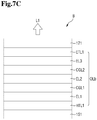
FIGS. 7A through 7C are enlarged cross-sectional views of an area B ofFIG. 5 ; -
FIG. 8 is an enlarged cross-sectional view of an area C ofFIG. 6 ; -
FIG. 9 is a graph illustrating the light reflectance of a pixel electrode with respect to the wavelength of light; -
FIG. 10 is a detailed plan view of pixels of a display area according to some embodiments; -
FIG. 11 is a cross-sectional view of a display device according to some embodiments; -
FIG. 12 is a cross-sectional view of a modified example of the display device according to the embodiment ofFIGS. 10 and11 ; -
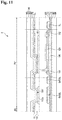
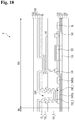
FIG. 13 is a detailed plan view of pixels of a display area according to some embodiments; -
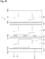
FIG. 14 is a cross-sectional view of a display device according to some embodiments; -
FIG. 15 is a detailed plan view of pixels of a display area according to some embodiments; -
FIG. 16 is a cross-sectional view of a display device according to some embodiments; -
FIG. 17 is a detailed plan view of pixels of a display area according to some embodiments; -
FIG. 18 is a cross-sectional view of a display device according to some embodiments; -
FIG. 19 is a detailed plan view of pixels of a display area according to some embodiments; -
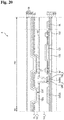
FIG. 20 is a cross-sectional view of a display device according to some embodiments; -
FIG. 21 is a detailed plan view of pixels of a display area according to some embodiments; -
FIG. 22 is a cross-sectional view of a display device according to some embodiments; -
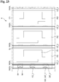
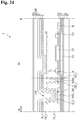
FIG. 23 is a detailed plan view of pixels of a display area according to some embodiments; and -
FIG. 24 is a cross-sectional view of a display device according to some embodiments. - Hereinafter, aspects of some embodiments of the present invention will be described with reference to the attached drawings.
- The aspects and features of the invention and methods for achieving the aspects and features will be more apparent by referring to the embodiments to be described in more detail with reference to the accompanying drawings. However, the invention is not limited to the embodiments disclosed hereinafter, but can be implemented in diverse forms. The matters defined in the description, such as the detailed construction and elements, are nothing but specific details provided to assist those of ordinary skill in the art in a comprehensive understanding of the invention, and the invention is only defined within the scope of the appended claims, and their equivalents.
- Where an element is described as being related to another element such as being "on" another element or "located on" a different layer or a layer, it includes both a case where an element is located directly on another element or a layer and a case where an element is located on another element via another layer or still another element. In contrast, where an element is described as being is related to another element such as being "directly on" another element or "located directly on" a different layer or a layer, it indicates a case where an element is located on another element or a layer with no intervening element or layer therebetween.
-
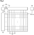
FIG. 1 is a schematic block diagram of adisplay device 1 according to some embodiments.FIG. 2 is a circuit diagram of an example of a first pixel PX1.FIG. 3 is a detailed plan view of thedisplay device 1 according to some embodiments. - The
display device 1 may be, for example, an organic light emitting diode display device (OLED). In the following embodiments, a case where an OLED is applied as thedisplay device 1 will be described as an example. However, other types of display devices such as a liquid crystal display device (LCD), a quantum-nano light emitting display device, a micro light emitting diode (LED) device, a field emission display device and an electrophoresis device are also applicable. - Referring to
FIGS. 1 through 3 , thedisplay device 1 according to some embodiments may include alight providing unit 100 and alight converting unit 200. Thedisplay device 1 may further include a driving unit. For example, the driving unit may include anintegrated driver circuit 300, ascan driver circuit 400, and apower supply circuit 600. Theintegrated driver circuit 300 may include adata driver 310 and atiming controller 320. Further, thelight providing unit 100 may include a scan line SL connected to thescan driver circuit 400, a data line DL connected to thedata driver 310, and a high potential voltage line VDDL and a low potential voltage line VSSL connected to thepower supply circuit 600. The scan line SL, the data line DL, the high potential voltage line VDDL, and the low potential voltage line VSSL may each be provided in plural numbers. - The
display device 1 may include a display area DA which displays an image and a non-display area NA which does not display an image. The driving unit and/or pads connected to the driving unit may be located on or at a side of the non-display area NA. - The display area DA may include a plurality of pixels. The pixels may include the first pixel PX1 that emits red light having a peak wavelength in the range of about 610 nm to about 650 nm, a second pixel PX2 that emits green light having a peak wavelength in the range of about 510 nm to about 550 nm, and a third pixel PX3 that emits blue light having a peak wavelength in the range of about 430 nm to about 470 nm. The second pixel PX2 may be located on or at a side of the first pixel PX1 in a first direction DR1. The third pixel PX3 may be located on or at a side of the second pixel PX2 in the first direction DR1.
- The first pixel PX1, the second pixel PX2, and the third pixel PX3 may be alternately arranged along a matrix direction (e.g., along a row or column in a matrix of pixels). The pixels PX1 through PX3 may be arranged in various ways such as a stripe type or a pentile type.
- The wavelength of light output from each of the pixels PX1 through PX3 may be adjusted not only by light emitted from a light emitting region in which a pixel electrode in each of the pixels PX1 through PX3 is exposed by a bank layer, but also by a wavelength conversion layer or a color filter overlapping the light emitting region.
- The non-display area NA may be arranged around the display area DA to surround the display area DA. The non-display area NA may include a dummy light emitting region having substantially the same structure as the light emitting region but controlled not to emit light. Alternatively, the non-display area NA may include the light emitting region, but the emission of light in a display direction may be blocked by a light shielding member.
- The
power supply circuit 600 may generate voltages VSS and VDD required for driving thelight providing unit 100 from main power supplied from a system board and supply the voltages VSS and VDD to thelight providing unit 100 through the high potential voltage lines VDDL and the low potential voltage lines VSSL. - The high potential voltage lines VDDL may include a main high potential voltage line MVDDL and sub high potential voltage lines SVDDL branching from the main high potential voltage line MVDDL. The main high potential voltage line MVDDL may extend in the first direction DR1 in the non-display area NA adjacent to a lower short side of the display area DA.
- The sub high potential voltage lines SVDDL may branch from the main high potential voltage line MVDDL located in the non-display area NA adjacent to the lower short side of the display area DA and extend in one direction. For example, the sub high potential voltage lines SVDDL may extend from the main high potential voltage line MVDDL to the display area DA along a second direction DR2 and pass the first through third pixels PX1 through PX3, respectively. The sub high potential voltage lines SVDDL may be electrically connected to transistors of the pixels PX1 through PX3, respectively. For example, the sub high potential voltage lines SVDDL may be electrically connected to source electrodes of driving transistors DT of the pixels PX1 through PX3 and provide a high potential voltage VDD received from the
power supply circuit 600 to the driving transistors DT, respectively. - The low potential voltage lines VSSL may include a main low potential voltage line MVSSL and a sub low potential voltage line SVSSL. The main low potential voltage line MVSSL and the sub low potential voltage line SVSSL may each be provided in plurality numbers.
- The main low potential voltage lines MVSSL may extend along the non-display area NA adjacent to edges of the display area DA. That is, the main low potential voltage lines MVSSL may surround the display area DA. The main low potential voltage lines MVSSL may be electrically connected to a common electrode (e.g., a cathode) of organic light emitting elements in the non-display area NA and provide a low potential voltage VSS to the common electrode.
- The sub low potential voltage lines SVSSL may branch from the main low potential voltage line MVSSL adjacent to the lower short side of the display area DA and extend in one direction. For example, the sub low potential voltage lines SVSSL may extend from the main low potential voltage line MVSSL to the display area DA in the second direction DR2 and may be located on the display area DA. In addition, the sub low potential voltage lines SVSSL may connect the main low potential voltage lines MVSSL located on the upper and lower short sides of the display area DA.
- The sub low potential voltage lines SVSSL may pass the first pixels PX1, but may not pass the second pixels PX2 and the third pixels PX3. However, the present disclosure is not limited to this case, and the sub low potential voltage lines SVSSL may also be respectively located in the first through third pixels PX1 through PX3 emitting light of different colors.
- The
integrated driver circuit 300 outputs signals and voltages for driving thelight providing unit 100. Thedata driver 310 of theintegrated driver circuit 300 receives digital video data DATA and a source control signal DCS from thetiming controller 320. Thedata driver 310 converts the digital video data DATA into analog data voltages according to the source control signal DCS and supplies the analog data voltages to the data lines DL of thelight providing unit 100. That is, the data voltages of theintegrated driver circuit 300 may be applied to the data lines DL. - Each of the data lines DL may be electrically connected to the
data driver 310 of theintegrated driver circuit 300 and extend in one direction to pass the display area DA. For example, each of the data lines DL may extend in the second direction DR2. The data lines DL may pass the first through third pixels PX1 through PX3, respectively. The data lines DL may be electrically connected to transistors of the pixels PX1 through PX3, respectively. For example, the data lines DL may be electrically connected to drain electrodes of scan transistors ST of the pixels PX1 through PX3, respectively. - The
timing controller 320 receives the digital video data DATA and timing signals from a host system. In addition, thetiming controller 320 generates control signals for controlling operation timings of thedata driver 310 and thescan driver 400. The control signals may include the source control signal DCS for controlling the operation timing of thedata driver 310 and a scan control signal SCS for controlling the operation timing of thescan driver 400. - The
scan driver 400 receives the scan control signal SCS from thetiming controller 320. Thescan driver 400 generates scan signals according to the scan control signal SCS and supplies the scan signals to the scan lines SL of thelight providing unit 100. Each of the scan lines SL is connected to thescan driver 400 and extends in one direction, for example, in the first direction DR1 to pass the display area DA. One scan line SL may pass the first through third pixels PX1 through PX3. In this case, the scan line SL may be electrically connected to a transistor of each of the pixels PX1 through PX3. For example, the scan line SL may be electrically connected to a gate electrode of the scan transistor ST of each of the pixels PX1 through PX3. - Referring to
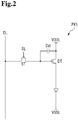
FIG. 2 , as described above, each of the first through third pixels PX1 through PX3 may be connected to at least one of the data lines DL, at least one of the scan lines SL, and a high potential voltage line VDDL. A first pixel PX1 may include a plurality of transistors for supplying an electric current to organic light emitting elements LD and at least one capacitor as illustrated inFIG. 2 . - Each of the organic light emitting elements LD may include a pixel electrode, an organic layer, and a common electrode. Here, the pixel electrode may be an anode, and the common electrode may be a cathode.
- The transistors may include the driving transistor DT which supplies an electric current to the organic light emitting elements LD and the scan transistor ST which supplies a data voltage to a gate electrode of the driving transistor DT, as illustrated in
FIG. 2 . The driving transistor DT and the scan transistor ST may be formed as thin-film transistors. - The driving transistor DT may include the gate electrode connected to a source electrode of the scan transistor ST, the source electrode connected to the high potential voltage line VDDL to which the high potential voltage VDD is applied, and a drain electrode connected to the pixel electrodes of the organic light emitting elements LD. The scan transistor ST may include the gate electrode connected to a scan line SL, the source electrode connected to the gate electrode of the driving transistor DT, and the drain electrode connected to a data line DL.
- A capacitor Cst is formed between the gate electrode and the source electrode of the driving transistor DT. The storage capacitor Cst stores a difference between a gate voltage and a source voltage of the driving transistor DT.
- In
FIG. 2 , a case where each of the first through third pixels PX1 through PX3 is a 2 transistor-1 capacitor (2T1C) pixel including one driving transistor DT, one scan transistor ST and one capacitor Cst is illustrated as an example. However, the present disclosure is not limited to this case, and each of the first through third pixels PX1 through PX3 may also include a plurality of scan transistors ST and a plurality of capacitors Cst. - The second and third pixels PX2 and PX3 can be represented by substantially the same circuit diagram as the first pixel PX1, and thus a detailed description thereof is omitted.
-
FIG. 4 is a schematic plan view of an area A ofFIG. 3 . InFIG. 4 , only a sub high potential voltage line SVDDL, a sub low potential voltage line SVSSL, a data line DL, apixel electrode 151 and acommon electrode 171 located in each of the pixels PX1 through PX3 are illustrated for ease of description. - The
pixel electrode 151 may be located in each of the pixels PX1 through PX3. Thepixel electrodes 151 respectively located in the pixels PX1 through PX3 may be spaced apart from each other. - The sub high potential voltage line SVDDL, the sub low potential voltage line SVSSL, and the data line DL may be in the display area DA.
- The sub low potential voltage line SVSSL may be located on a side of the
pixel electrode 151 of the first pixel PX1. The sub low potential voltage line SVSSL may be in the first pixel PX1 but not in the second pixel PX2 and the third pixel PX3 as described above. In addition, the low potential voltage line SVSSL may be in another pixel located on a side of the third pixel PX3 in the first direction DR1. - In the first pixel PX1, the sub high potential voltage line SVDDL may be between the sub low potential voltage line SVSSL and the
pixel electrode 151. The sub high potential voltage line SVDDL may be spaced apart from the sub low potential voltage line SVSSL. In each of the second pixel PX2 and the third pixel PX3, the sub high potential voltage line SVDDL may be located between therespective pixel electrodes 151 of adjacent pixels (e.g., PX2 and PX3). - In the first pixel PX1, the data line DL may be located between the sub high potential voltage line SVDDL of the second pixel PX2 and the
pixel electrode 151 of the first pixel PX1. In the second pixel PX2, the data line DL may be located between thepixel electrode 151 of the second pixel PX2 and the sub high potential voltage line SVDDL of the adjacent third pixel PX3. In the third pixel PX3, the data line DL may be located between thepixel electrode 151 of the third pixel PX3 and the sub high potential voltage line SVDDL of a right adjacent pixel. - A planar width W1 of the sub low potential voltage line SVSSL may be greater than a planar width W2 of the sub high potential voltage line SVDDL and a planar width W3 of the data line DL. In addition, the planar width W2 of the sub high potential voltage line SVDDL may be, but is not limited to, greater than the planar width W3 of the data line DL.
- The
common electrode 171 may be arranged over the whole surface of the display area DA. - The cross-sectional structure of the
display device 1 will now be described in more detail. -
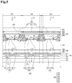
FIG. 5 is a cross-sectional view taken along the line VI-VI' ofFIG. 4 .FIG. 6 is a cross-sectional view taken along line VII-VII' ofFIG. 4 .FIGS. 7A through 7C are enlarged cross-sectional views of an area B ofFIG. 5 . InFIG. 5 , the configuration of thelight providing unit 100 is schematically illustrated for ease of description. For example,FIG. 5 illustrates only drainelectrodes 141 connected to thepixel electrodes 151, thepixel electrodes 151 and thecommon electrode 171 among a plurality of electrodes of thelight providing unit 100 ofFIG. 6 and illustrates only aplanarization layer 161, abank layer 162 and a thin-film encapsulation layer 180 among inorganic and/or organic films of thelight providing unit 100. In addition,FIG. 6 does not illustrate elements arranged above thelight providing unit 100 illustrated inFIG. 5 . - Referring to
FIGS. 5 through 7 , thelight providing unit 100 may include a base substrate, a plurality of electrodes, wirings, a plurality of inorganic and/or organic films having an insulation function, a planarization function and an encapsulation function, and a plurality of organic light emitting elements, each including thepixel electrode 151, an organic layer OL and thecommon electrode 171. - A
first base substrate 101 may support various elements arranged on thefirst base substrate 101. Thefirst base substrate 101 may be a rigid substrate containing a rigid material such as glass or quartz. Alternatively, thefirst base substrate 101 may be a flexible substrate containing a ductile material. - A
buffer layer 102 may be located on thefirst base substrate 101. Thebuffer layer 102 may prevent or reduce diffusion of impurity ions, prevent or reduce penetration of moisture or outside air, and perform a surface planarization function. - A
semiconductor layer 105 may be arranged on thebuffer layer 102. Thesemiconductor layer 105 forms a channel of a thin-film transistor TFT. Thesemiconductor layer 105 may be located in each of the pixels PX1 through PX3 of the display area DA. Thesemiconductor layer 105 may include polycrystalline silicon, amorphous silicon, an oxide semiconductor, etc. - A first insulating
layer 111 which is a gate insulating film may be arranged on thesemiconductor layer 105. - A gate conductive layer may be arranged on the first insulating
layer 111. The gate conductive layer may include agate electrode 121 of the thin-film transistor TFT. The gate conductive layer may further include a signal scan line which transmits a scan signal to a first electrode of a storage capacitor and thegate electrode 121. - A second insulating
layer 112 and a thirdinsulating layer 113 may be sequentially stacked on the gate conductive layer. A capacitor electrode may be located between the second insulatinglayer 112 and the third insulatinglayer 113. - A source/drain conductive layer may be arranged on the third insulating
layer 113. The source/drain conductive layer may include a sub low potential voltage line SVSSL, a sub high potential voltage line SVDDL, adrain electrode 141 and asource electrode 142 of the thin-film transistor TFT, and a data line DL. Thedrain electrode 141 and thesource electrode 142 of the thin-film transistor TFT may respectively be electrically connected to a drain region and a source region of thesemiconductor layer 105 through contact holes passing through the third insulatinglayer 113, the second insulatinglayer 112 and the first insulatinglayer 111. The sub low potential voltage line SVSSL, the sub high potential voltage line SVDDL, and thedrain electrode 141 and thesource electrode 142 of the thin-film transistor TFT are spaced apart from each other. - The source/drain conductive layer may include one or more metals selected from aluminium (Al), platinum (Pt), palladium (Pd), silver (Ag), magnesium (Mg), gold (Au), nickel (Ni), neodymium (Nd), iridium (Ir), chromium (Cr), calcium (Ca), titanium (Ti), tantalum (Ta), tungsten (W), copper (Cu), and molybdenum (Mo). The source/drain conductive layer may be a single film as illustrated in the drawings. However, the source/drain conductive layer is not limited to the single film and may also be a multifilm. For example, the source/drain conductive layer may have a stacked structure of Ti/Al/Ti, Mo/AI/Mo, Mo/AIGe/Mo, or Ti/Cu.
- The
planarization layer 161 may be arranged on the source/drain conductive layer. Theplanarization layer 161 may planarize each region in which thepixel electrode 151 is arranged on theplanarization layer 161. - The
planarization layer 161 may include contact holes, each exposing an upper surface of thedrain electrode 141. Thepixel electrode 151 may contact and be electrically connected to the upper surface of thedrain electrode 141 exposed through each of the contact holes of theplanarization layer 161. - The
planarization layer 161 may include an organic insulating material such as polyacrylate resin, epoxy resin, phenolic resin, polyamide resin, polyimide resin, unsaturated polyester resin, polyphenylenether resin, polyphenylenesulfide resin, or benzocyclobutene (BCB). - The
pixel electrode 151 may be arranged on theplanarization layer 161 in each of the pixels PX1 through PX3. Thepixel electrode 151 may include a stack of a lower film, a reflective film, and an upper film. The stacked films of thepixel electrode 151 will be described later. - The
bank layer 162 may be located on thepixel electrode 151. Thebank layer 162 may be arranged in a lattice shape along the boundaries of the pixels PX1 through PX3. Thebank layer 162 may include open portions arranged in a lattice shape and each at least partially exposing thepixel electrode 151. Thebank layer 162 may be made of an organic film or an inorganic film. In addition, thebank layer 162 may be made of a stack of an inorganic film and an organic film. - The organic layer OL may be arranged on the
pixel electrode 151 exposed by each of the open portions of thebank layer 162. Although the organic layer OL is illustrated as a single piece formed without distinction between the pixels PX1 through PX3, it may also be divided into separate pieces formed in the pixels PX1 through PX3, respectively. - The organic layer OL includes an organic light emitting layer. In the organic light emitting layer, electrons and holes provided from an anode and a cathode may recombine to generate excitons. As the generated excitons change from an excited state to a ground state, blue light may be emitted. The organic layer OL may further include an auxiliary layer which assists the injection/movement of holes and electrons. The organic layer OL will now be described in more detail with reference to
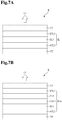
FIGS. 7A through 7C . - In an embodiment, referring to
FIG. 7A , the organic layer OL may include a first hole transport layer HTL1 arranged on thepixel electrode 151 of the first pixel PX1, a first light emitting layer EL1 arranged on the first hole transport layer HTL1, and a first electron transport layer ETL1 arranged on the first light emitting layer EL1. In the current embodiment, the organic layer OL may include only one light emitting layer, for example, the first light emitting layer EL1, and the first light emitting layer EL1 may emit blue light L1. - In an embodiment, referring to
FIG. 7B , an organic layer OLa may further include a first charge generation layer CGL1 arranged on a first light emitting layer EL1 and a second light emitting layer EL2 arranged on the first charge generation layer CGL1, and a first electron transport layer ETL1 may be arranged on the second light emitting layer EL2. The first charge generation layer CGL1 may inject electric charges into each of the light emitting layers EL1 and EL2. - In an embodiment, referring to
FIG. 7C , an organic layer OLb may include three light emitting layers EL1 through EL3 and two charge generation layers CGL1 and CGL2 interposed between the light emitting layers EL1 through EL3. That is, the organic layer OLb may further include a first charge generation layer CGL1 located on a first light emitting layer EL1, a second light emitting layer EL2 located on the first charge generation layer CGL1, a second charge generation layer CGL2 located on the second light emitting layer EL2, and a third light emitting layer EL3 located on the second charge generation layer CGL2. A first electron transport layer ETL1 may be located on the third light emitting layer EL3. - The second light emitting layer EL2 and/or the third light emitting layer EL3 may emit blue light having the same or different peak wavelength as that of blue light emitted from the first light emitting layer EL1.
- Referring again to
FIGS. 5 and6 , when thepixel electrode 151 is an anode of an organic light emitting element, thecommon electrode 171 may be a cathode of the organic light emitting element. Thecommon electrode 171 may include a low work function material into which electrons can be easily injected, such as Li, Ca, LiF/Ca, LiF/AI, Al, Mg, Ag, Pt, Pd, Ni, Au, Nd, Ir, Cr, BaF, Ba, or a compound or mixture of the same (e.g., a mixture of Ag and Mg). - The
common electrode 171 may have transparency or translucency. If the above low work function material is formed to a thickness as small as tens to hundreds of angstroms, thecommon electrode 171 may have transparency or translucency. When a thin metal film having a low work function is used, thecommon electrode 171 may further include a transparent conductive material layer stacked on the thin metal film in order to secure transparency and reduce resistance. The transparent conductive material layer may be tungsten oxide (WxOx), titanium oxide (TiO2), indium tin oxide (ITO), indium zinc oxide (IZO), zinc oxide (ZnO), indium tin zinc oxide (ITZO), magnesium oxide (MgO), or the like. - The thin-
film encapsulation layer 180 may be arranged on thecommon electrode 171. To prevent or reduce the introduction of impurities or moisture from the outside, the thin-film encapsulation layer 180 may be arranged on the organic light emitting elements to encapsulate thelight providing unit 100. The thin-film encapsulation layer 180 may be arranged over the whole surface regardless of the pixels PX1 through PX3. The thin-film encapsulation layer 180 may cover the organic light emitting elements including thecommon electrode 171 arranged under the thin-film encapsulation layer 180. The organic light emitting elements may be surrounded and encapsulated by thefirst base substrate 101 and the thin-film encapsulation layer 180. - The thin-
film encapsulation layer 180 may include a first encapsulatinginorganic film 181, an encapsulatingorganic film 182, and a second encapsulatinginorganic film 183 sequentially stacked on thecommon electrode 171. The first encapsulatinginorganic film 181 may be arranged on a surface of thecommon electrode 171, the encapsulatingorganic film 182 may be arranged on a surface of the first encapsulatinginorganic film 181, and the second encapsulatinginorganic film 183 may be arranged on a surface of the encapsulatingorganic film 182. - The
light converting unit 200 will now be described. Thelight converting unit 200 may include asecond base substrate 201,light shielding members color filters 231 through 233,light conversion patterns 251 through 253, and a plurality of stacked capping layers 241 through 243. - The
second base substrate 201 is located opposite thefirst base substrate 101. Thesecond base substrate 201 may be made of a material selected from the example materials of thefirst base substrate 101. - A first
light shielding member 220 may be arranged on a surface of thesecond base substrate 201 in a direction facing the light providing unit 100 (in a downward direction inFIG. 6 ). The firstlight shielding member 220 may be arranged at boundaries of light outputting regions PA1 through PA3, that is, in a non-light outputting region PB to block transmission of light. The firstlight shielding member 220 may prevent or reduce color mixing of light between the pixels PX1 through PX3. The firstlight shielding member 220 may include at least one of an organic material, a metal material including chromium, and carbon black. -
Color filters 230 may be arranged on the surface of thesecond base substrate 201. The color filters 230 may include first throughthird color filters 231 through 233. The color filters 231 through 233 may be arranged in the pixels PX1 through PX3, respectively. Each of the first throughthird color filters 231 through 233 may be an absorptive filter that absorbs light of a specific wavelength and transmits light of another specific wavelength. - The
first color filter 231 may block or absorb blue light L1 among the blue light L1 and red light L2 output from a firstwavelength conversion pattern 251. That is, thefirst color filter 231 may function as a blue light blocking filter that blocks blue light and may function as a red light transmitting filter that selectively transmits the red light L2. Thefirst color filter 231 may include a red colorant. - The
second color filter 232 may block or absorb blue light L1 among the blue light L1 and green light L3 output from a secondwavelength conversion pattern 252. That is, thesecond color filter 232 may function as a blue light blocking filter that blocks blue light and may function as a green light transmitting filter that selectively transmits the green light L3. Thesecond color filter 232 may include a green colorant. - The
third color filter 233 may function as a blue light transmitting filter that transmits blue light L4 output from alight transmission pattern 253. Thethird color filter 233 may include a blue colorant. - A
first capping layer 241 may be located on thefirst color filter 231, thesecond color filter 232 and thethird color filter 233 to prevent or reduce introduction of outside air and moisture. Thefirst capping layer 241 may be arranged over the whole surface of thecolor filters 231 through 233. - A
second capping layer 242 may be located on thefirst capping layer 241 to prevent or reduce thecolor filters 230 from being damaged and/or contaminated. Thesecond capping layer 242 may cover thefirst capping layer 241. - The
first capping layer 241 and thesecond capping layer 242 may be made of an inorganic material. For example, thefirst capping layer 241 and thesecond capping layer 242 may be made of silicon nitride, aluminium nitride, zirconium nitride, titanium nitride, hafnium nitride, tantalum nitride, silicon oxide, aluminium oxide, titanium oxide, tin oxide, cerium oxide, or silicon oxynitride. -
Light conversion patterns 250 may be arranged on thefirst capping layer 241 and thesecond capping layer 242. Thelight conversion patterns 250 may include the firstwavelength conversion pattern 251, the secondwavelength conversion pattern 252, and thelight transmission pattern 253. Thelight conversion patterns 251 through 253 may be arranged in the pixels PX1 through PX3, respectively. - The first
wavelength conversion pattern 251 arranged in the first pixel PX1 may convert the blue light L1 into the red light L2 and output the red light L2. - The first
wavelength conversion pattern 251 may include afirst base resin 2511 and afirst wavelength shifter 2512 dispersed in thefirst base resin 2511 and may further include afirst scatterer 2513 dispersed in thefirst base resin 2511. - The
first base resin 2511 may include an organic material such as epoxy resin, acrylic resin, cardo resin, or imide resin. - The
first wavelength shifter 2512 may convert or shift a peak wavelength of incident light into another specific peak wavelength. Examples of thefirst wavelength shifter 2512 may include quantum dots, quantum bars, and phosphors. - A portion of the blue light L1 emitted from a light emitting region of the first pixel PX1 may be transmitted through the first
wavelength conversion pattern 251 without being converted into the red light L2 by thefirst wavelength shifter 2512. This portion of the blue light L1 which is incident on thefirst color filter 231 without being converted by the firstwavelength conversion pattern 251 may be blocked by thefirst color filter 231. On the other hand, the red light L2 into which the blue light L1 has been converted by the firstwavelength conversion pattern 251 may be transmitted to the outside through thefirst color filter 231. - The
first scatterer 2513 may be light scattering particles. Thefirst scatterer 2513 may be metal oxide particles or organic particles. - The second
wavelength conversion pattern 252 located in the second pixel PX2 may convert the blue light L1 into the green light L3 in the range of about 510 nm to about 550 nm and output the green light L3. - The second
wavelength conversion pattern 252 may include asecond base resin 2521 and asecond wavelength shifter 2522 dispersed in thesecond base resin 2521 and may further include asecond scatterer 2523 dispersed in thesecond base resin 2521. - The
second base resin 2521 may be made of the same material as thefirst base resin 2511 or may include at least one of the materials mentioned as examples of the material of thefirst base resin 2511. - The
second wavelength shifter 2522 may convert or shift a peak wavelength of incident light into another specific peak wavelength. Thesecond wavelength shifter 2522 may convert the blue light L1 having a peak wavelength in the range of 430 nm to 470 nm into the green light L3 having a peak wavelength in the range of 510 nm to 550 nm. A portion of the blue light L1 may be transmitted through the secondwavelength conversion pattern 252 without being converted into the green light L3 by thesecond wavelength shifter 2522. This portion of the blue light L1 may be blocked by thesecond color filter 232. On the other hand, the green light L3 into which the blue light L1 has been converted by the secondwavelength conversion pattern 252 may be transmitted to the outside through thesecond color filter 232. - The
second wavelength shifter 2522 is substantially the same or similar to thefirst wavelength shifter 2512 described above, and thus a detailed description thereof is omitted. - The
second scatterer 2523 is substantially the same or similar to thefirst scatterer 2513 described above, and thus a detailed description thereof is omitted. - The
light transmission pattern 253 located in the third pixel PX3 may transmit the incident blue light L1 as it is. - The
light transmission pattern 253 may further include athird base resin 2531 and athird scatterer 2533 dispersed in thethird base resin 2531. - The
third base resin 2531 may be made of the same material as thefirst base resin 2511 or may include at least one of the materials mentioned as examples of the material of thefirst base resin 2511. - The
third scatterer 2533 is substantially the same or similar to thefirst scatterer 2513 described above, and thus a detailed description thereof is omitted. - A
third capping layer 243 may be arranged on thelight conversion patterns 250. Thethird capping layer 243 may cover thelight conversion patterns 250. Thethird capping layer 243 may include an inorganic material. Thethird capping layer 243 may be made of the same material as thefirst capping layer 241 or may include at least one of the materials mentioned in the description of thefirst capping layer 241. In an embodiment, thethird capping layer 243 may include silicon nitride. - An organic planarization layer planarizing a lower step of the
light conversion patterns 250 and an inorganic capping layer covering the organic planarization layer may be further arranged on thethird capping layer 243, but the present disclosure is not limited to this case. - A plurality of second
light shielding patterns 260 may be arranged on thethird capping layer 243 in the non-light outputting region PB. The secondlight shielding patterns 260 may prevent or reduce color mixing between adjacent pixels PX1 through PX3. In an example, the secondlight shielding patterns 260 may include at least one of the materials mentioned as examples of the material of the firstlight shielding member 220. - A
filler 700 may be arranged between the light providingunit 100 and thelight converting unit 200. Thefiller 700 may contact the thin-film encapsulation layer 180 of thelight providing unit 100 and contact thethird capping layer 243 and the secondlight shielding patterns 260 of thelight converting unit 200. - The
filler 700 may planarize a surface step formed by thelight conversion patterns 251 through 253 and the secondlight shielding patterns 260. Thefiller 700 may be made of a material having a buffer function and serve as a buffer member that absorbs shocks generated between the light providingunit 100 and thelight converting unit 200. For example, thefiller 700 may be made of a silicon-based organic material, an epoxy-based organic material, or an acrylic-based organic material. - The
pixel electrode 151 will now be described in more detail with reference toFIGS. 8 and9 . -
FIG. 8 is an enlarged cross-sectional view of an area C ofFIG. 6 .FIG. 9 is a graph illustrating the light reflectance of thepixel electrode 151 with respect to the wavelength range of light.FIG. 9 illustrates the reflectance (%) (the vertical axis) with respect to the wavelength range (nm) (the horizontal axis) of light in a case where an aluminum alloy (AlNiX) is applied as an example of a reflective film. To help understand the present disclosure, a case where silver (Ag) is applied as the reflective film is also illustrated. - The
pixel electrode 151 according to an embodiment may have a multilayer structure as mentioned above. Thepixel electrode 151 may include alower film 152, anupper film 154 arranged opposite thelower film 152, and areflective film 153 interposed between thelower film 152 and theupper film 154. - The
lower film 152 may increase the adhesion of thepixel electrode 151 to theplanarization layer 161 located under thepixel electrode 151. Thelower film 152 may include, for example, indium-tin-oxide (ITO), indium-zinc-oxide (IZO), zinc oxide (ZnO), or indium oxide (In2O3). Also, thelower film 152 may include, for example, indium-tin-oxide (ITO), indium-zinc-oxide (IZO), zinc oxide (ZnO), indium-tin-zinc-oxide (ITZO) or magnesium oxide (MgO). - The
upper film 154 may include a high work function material into which holes can be easily injected. For example, theupper film 154 may include the same material as thelower film 152. - Referring to
FIG. 8 , light Li provided toward thepixel electrode 151 may include light L11 emitted downward from the organic layer OL and light L12 emitted upward from the organic layer OL and then reflected downward by thecommon electrode 171. The light Li may further include light reflected downward by an element located above thecommon electrode 171. The incident light Li may be light having the same peak wavelength range as the blue light L1. However, the present disclosure is not limited to this case, and the incident light Li may further include light having the same or similar peak wavelength range as the red light L2 and the green light L3. - The light Li provided toward the
pixel electrode 151 may be reflected upward by thepixel electrode 151. For example, the light Li provided toward thepixel electrode 151 may be reflected upward by theupper film 154 or thereflective film 153. - Reflectance, as used herein, denotes the reflectance of the
pixel electrode 151 and may be defined as a ratio of light LR1 and L R2 reflected upward by theupper film 154 or thereflective film 153 to the light Li provided toward thepixel electrode 151. - When the
pixel electrode 151 includes thereflective film 153, the proportion of the light LR2 reflected upward by thereflective film 153 in the light Li provided toward thepixel electrode 151 may be increased. That is, the overall reflectance may be increased. - The
lower film 152 may have a first thickness T1, thereflective film 153 may have a second thickness T2, and theupper film 154 may have a third thickness T3. The thicknesses T1 and T3 of thelower film 152 and theupper film 154 may be smaller than the thickness T2 of thereflective film 153. - For example, the thickness T1 of the
lower film 152 and the thickness T3 of theupper film 154 may be about 30 Å to about 200 Å. - The thickness T2 of the
reflective film 153 may be about 300 Å or more. The thickness T2 of thereflective film 153 may be adjusted in view of process stability, reflection efficiency, and thinning. For example, when the thickness T2 of thereflective film 153 is about 300 Å or more, thereflective film 153 can be stably formed on thelower film 152 through a sputtering process. - Further, when the thickness T2 of the
reflective film 153 is about 600 Å or more, the reflectance of thepixel electrode 151 may be about 80% or more over the entire wavelength range (350 nm to 750 nm) on the horizontal axis. That is, an effective thickness that enables thereflective film 153 to have a reflection efficiency of about 80% or more for the incident light Li may be about 600 Å or more. - On the other hand, the thickness T2 of the
reflective film 153 may be 1500 Å or less in view of thinning. - In addition, as the thickness T2 of the
reflective film 153 increases, the overall resistance of theupper film 154 and thelower film 152 arranged on and under thereflective film 153 may be reduced linearly and/or non-linearly. Even in this case, the thickness of AINiLa may be adjusted to about 600 Å to about 1500 Å in view of reflection efficiency and thinning. - The
reflective film 153 may be made of any material having a reflectance of about 80% or more over the entire wavelength range of blue light, as will be described inFIG. 9 . The material may be an aluminium-nickel alloy (AlNiX), where X may include one or more elements selected from La, Ce, Pr, Pm, Sm, Eu, Gd, Tb, Dy, Ho, Er, Tm, Tb and Lu. For example, X may be lanthanum (La), and AINiX may be aluminium-nickel-lanthanum (AlNiLa). - Referring to
FIG. 9 , when thereflective film 153 according to the embodiment is applied, the reflectance may be about 80% or more over the entire wavelength range (about 420 nm to about 470 nm) of blue light. InFIG. 9 , thepixel electrode 151 having an aluminium-nickel-alloy (AlNiX) as thereflective film 153 is illustrated. The average reflectance of light LR reflected upward by thepixel electrode 151 among the light Li provided toward thepixel electrode 151 is within the range of about 80% to about 90% over the entire wavelength range of blue light. - The reflectance of the
pixel electrode 151 in other wavelength ranges excluding the wavelength range of blue light may also be about 80% to about 90%. For example, the difference between the average reflectance of thepixel electrode 151 in the wavelength range (about 510 nm to about 550 nm) of green light and the average reflectance of thepixel electrode 151 in the wavelength range (about 420 nm to about 470 nm) of the blue light may be about 5% or less. - A
pixel electrode 151 including silver (Ag) as a reflective film may have a higher reflectance than thepixel electrode 151 according to the embodiment for light having a wavelength (of more than about 470 nm) longer than that of blue light, but has a lower reflectance than thepixel electrode 151 according to the embodiment for light having a wavelength (of less than about 470 nm) shorter than that of the blue light. - In an embodiment, a blue organic light emitting element is applied as described above. The
pixel electrode 151 according to the embodiment includes, as thereflective film 153, a material having superior reflectance in the wavelength range of blue light. Therefore, a pixel electrode including a material other than the above material as the material of a reflective film may have a higher reflectance than thepixel electrode 151 according to the embodiment in a wavelength range (more than about 470 nm) longer than the wavelength range of blue light. However, the reflectance of thepixel electrode 151 according to the embodiment may be higher in the wavelength range of blue light and a wavelength range (less than about 470 nm) shorter than the above wavelength range. In this regard, thepixel electrode 151 according to the embodiment may be optimal for an organic light emitting element that emits blue light, thus improving the overall luminous efficiency of the blue organic light emitting element. - Hereinafter, other embodiments will be described. In the following embodiments, elements identical to those of the above-described embodiment will be indicated by the same reference numerals, and a description of the elements will be omitted or given briefly.
-
FIG. 10 is a detailed plan view of pixels of a display area according to some embodiments.FIG. 11 is a cross-sectional view of adisplay device 2 according to some embodiments.FIGS. 10 and11 correspond toFIGS. 4 and6 , respectively. - Referring to
FIGS. 10 and11 , thedisplay device 2 according to some embodiments is different from thedisplay device 1 ofFIGS. 5 through 7 in that it further includes anauxiliary line 152a, and theauxiliary line 152a contacts acommon electrode 171 through contact holes CNT of a bank layer 162_1. - For example, the
auxiliary line 152a may be arranged on the same layer aspixel electrodes 151 and spaced apart from thepixel electrodes 151. That is, theauxiliary line 152a may be electrically isolated from thepixel electrodes 151. Theauxiliary line 152a may include the same material as thepixel electrodes 151. - The
auxiliary line 152a may extend along one direction. For example, theauxiliary line 152a may be formed as a single piece and extend along the second direction DR2 (seeFIG. 2 ). Alternatively, theauxiliary line 152a may extend along the second direction DR2 but may be divided into island shapes. - The bank layer 162_1 may include the contact holes CNT that expose an upper surface of the
auxiliary line 152a. In addition, an organic layer overlapping the contact holes CNT of the bank layer 162_1 may be removed through a laser drilling process. Therefore, an organic layer OL_1 may not overlap the contact holes CNT of the bank layer 162_1 in a thickness direction and may be aligned with side surfaces of the bank layer 162_1. InFIG. 10 , three contact holes CNT are illustrated. However, the number of the contact holes CNT is not limited to three and may also be one, two, or four or more. - The
common electrode 171 may, as described above, include a low work function material into which electrons can be easily injected. In the case of a top emission display device, the low work function material may be formed to a thickness as small as tens to hundreds of angstroms to secure transparency or translucency. However, if the low work function material is thinned, the sheet resistance of thecommon electrode 171 may be increased. - The
display device 2 according to the current embodiment further includes theauxiliary line 152a formed on the same layer as thepixel electrodes 151 but electrically isolated from thepixel electrodes 151, and theauxiliary line 152a may contact thecommon electrode 171 through the contact holes CNT of the bank layer 162_1. Therefore, the area and/or thickness of the thinnedcommon electrode 171 in the thickness direction may be increased, thereby reducing the overall sheet resistance of thecommon electrode 171. - Further, when light emitted from the organic layer OL_1 is reflected or converted by a wavelength conversion pattern and then provided to a region where the
auxiliary line 152a is arranged, the light may be reflected again toward the display direction. For example, the light emitted from the organic layer OL_1 may be blue light, and the light provided after being converted by the wavelength conversion pattern may be green light and/or red light. Theauxiliary line 152a according to some embodiments may have a reflectance difference of about 5% or less in the wavelength range of about 350 nm to about 750 nm. Therefore, it can reflect light of the entire wavelength range in a substantially uniform ratio without variation in reflectance according to the wavelength range of light. As a result, the color purity of the display device may be improved. - In the current embodiment, a blue organic light emitting element is applied as described above. A
pixel electrode 151 according to the current embodiment includes, as areflective film 153, a material having superior reflectance in the wavelength range of blue light. Therefore, a pixel electrode including a material other than the above material as the material of a reflective film may have a higher reflectance than thepixel electrode 151 according to the embodiment in a wavelength range (more than about 470 nm) longer than the wavelength range of blue light. However, the reflectance of thepixel electrode 151 according to the embodiment may be higher in the wavelength range of blue light and a wavelength range (less than about 470 nm) shorter than the above wavelength range. In this regard, thepixel electrode 151 according to the embodiment may be optimal for an organic light emitting element that emits blue light, thus improving the overall luminous efficiency of the blue organic light emitting element. -
FIG. 12 is a cross-sectional view of a modified example of thedisplay device 2 according to the embodiment ofFIGS. 10 and11 . - Referring to
FIG. 12 , the display device is different from thedisplay device 2 ofFIGS. 10 and11 in that a light-blockingmaterial layer 191 is further arranged on side surfaces of a bank layer 162_1. - For example, when an organic layer OL_1 overlapping a contact hole CNT of the bank layer 162_1 is removed through the above-described laser drilling process, it may remain on the side surfaces of the bank layer 162_1. In this case, light may be emitted laterally from part of the side portions of the bank layer 162_1 due to a
pixel electrode 151 and acommon electrode 171. Therefore, after the laser drilling process on the organic layer OL_1, the light-blockingmaterial layer 191 may be arranged between the remaining material of the organic layer OL_1 on the side surfaces of the bank layer 162_1 and thecommon electrode 171. The light-blockingmaterial layer 191 may also be arranged between the organic layer OL_1 and thecommon electrode 171 in a non-light emitting region PB, but the present disclosure is not limited to this case. - The light-blocking
material layer 191 may include a material such as Liq. Therefore, the lateral light emission due to the remaining organic material of the organic layer OL_1 can be prevented or reduced. -
FIG. 13 is a detailed plan view of pixels of a display area according to some embodiments.FIG. 14 is a cross-sectional view of adisplay device 3 according to some embodiments. - Referring to
FIGS. 13 and14 , thedisplay device 3 according to the current embodiment is different from the embodiment ofFIGS. 11 and12 in that an auxiliary line 152_1 contacts a sub low potential voltage line SVSSL through contact holes CNT_1 of a planarization layer 161_1 and does not contact acommon electrode 171. - For example, the planarization layer 161_1 may include the contact holes CNT_1 that expose an upper surface of the sub low potential voltage line SVSSL.
- In
FIG. 13 , three contact holes CNT_1 are illustrated. However, the number of the contact holes CNT_1 is not limited to three and may also be one, two, or four or more. - The auxiliary line 152_1 electrically isolated from
pixel electrodes 151 may directly contact and be electrically connected to the upper surface of the sub low potential voltage line SVSSL exposed by the contact holes CNT_1. Therefore, the area and/or thickness of the sub low potential voltage line SVSSL in the thickness direction may be increased, thereby reducing the overall sheet resistance of the sub low potential voltage line SVSSL. - Further, when light emitted from an organic layer OL is reflected or converted by a wavelength conversion pattern and then provided to a region where the auxiliary line 152_1 is located, the light may be reflected again toward the display direction. The auxiliary line 152_1 according to the current embodiment may have a reflectance difference of about 5% or less in the wavelength range of about 350 nm to about 750 nm. Therefore, it can reflect light of the entire wavelength range in a substantially uniform ratio without variation in reflectance according to the wavelength range of light. As a result, the color purity of the display device can be improved.
-
FIG. 15 is a detailed plan view of pixels of a display area according to an embodiment.FIG. 16 is a cross-sectional view of adisplay device 4 according to an embodiment. - Referring to
FIGS. 15 and16 , thedisplay device 4 according to the current embodiment is different from the embodiment ofFIGS. 13 and14 in that each auxiliary line 152_2 contacts a corresponding sub high potential voltage line SVDDL through contact holes CNT_2 of a planarization layer 161_2 and does not contact a sub low potential voltage line SVSSL. - For example, the planarization layer 161_2 may include the contact holes CNT_2 which expose an upper surface of each sub high potential voltage line SVDDL. In
FIG. 15 , three contact holes CNT_2 are illustrated. However, the number of the contact holes CNT_2 is not limited to three and may also be one, two, or four or more. - Each auxiliary line 152_2 electrically isolated from
pixel electrodes 151 may directly contact and be electrically connected to the upper surface of a corresponding sub high potential voltage line SVDDL exposed by the contact holes CNT_2. Therefore, the area and/or thickness of each sub high potential voltage line SVDDL in the thickness direction may be increased, thereby reducing the overall sheet resistance of each sub high potential voltage line SVDDL. - Further, when light emitted from an organic layer OL is reflected or converted by a wavelength conversion pattern and then provided to a region where each auxiliary line 152_2 is located, the light may be reflected again toward the display direction. The auxiliary lines 152_2 according to the current embodiment may have a reflectance difference of about 5% or less in the wavelength range of about 350 nm to about 750 nm. Therefore, they can reflect light of the entire wavelength range in a substantially uniform ratio without variation in reflectance according to the wavelength range of light. As a result, the color purity of the display device can be improved.
-
FIG. 17 is a detailed plan view of pixels of a display area according to an embodiment.FIG. 18 is a cross-sectional view of adisplay device 5 according to an embodiment. - Referring to
FIGS. 17 and18 , in thedisplay device 5 according to the current embodiment, a sub low potential voltage line SVSSL, an auxiliary line 152_3, and acommon electrode 171 contact each other. That is, the embodiment ofFIGS. 17 and18 is a combination of the embodiments ofFIGS. 11 and14 . Therefore, a description of the same elements and features as those ofFIGS. 11 and14 will be omitted or given briefly, and the differences will be mainly described below. - A planarization layer 161_3 may include contact holes CNT_1 that expose an upper surface of the sub low potential voltage line SVSSL. The auxiliary line 152_3 electrically isolated from
pixel electrodes 151 may directly contact and be electrically connected to the upper surface of the sub low potential voltage line SVSSL exposed by the contact holes CNT_1. - In addition, a bank layer 162_1 may include contact holes CNT that expose an upper surface of the auxiliary line 152_3, and the auxiliary line 152_3 may contact the
common electrode 171 through the contact holes CNT of thebank layer 162 1. - Therefore, the area and/or thickness of the
common electrode 171 and the sub low potential voltage line SVSSL in the thickness direction may be increased, thereby reducing the overall sheet resistance of thecommon electrode 171 and the sub low potential voltage line SVSSL. - Further, when light emitted from an organic layer OL_1 is reflected or converted by a wavelength conversion pattern and then provided to a region where the auxiliary line 152_3 is located, the light may be reflected again toward the display direction. The auxiliary line 152_3 according to the current embodiment may have a reflectance difference of about 5% or less in the wavelength range of about 350 nm to about 750 nm. Therefore, it can reflect light of the entire wavelength range in a substantially uniform ratio without variation in reflectance according to the wavelength range of light. As a result, the color purity of the display device can be improved.
-
FIG. 19 is a detailed plan view of pixels of a display area according to an embodiment.FIG. 20 is a cross-sectional view of adisplay device 6 according to an embodiment. - Referring to
FIGS. 19 and20 , thedisplay device 6 ofFIGS. 19 and20 is a combination of the embodiment ofFIG. 11 and the embodiment ofFIG. 16 . Therefore, a detailed description of the current embodiment is omitted here and can be found in the description ofFIGS. 11 and16 . -
FIG. 21 is a detailed plan view of pixels of a display area according to an embodiment.FIG. 22 is a cross-sectional view of adisplay device 7 according to an embodiment. Referring toFIGS. 21 and22 , thedisplay device 7 ofFIGS. 21 and22 is a combination of the embodiment ofFIG. 14 and the embodiment ofFIG. 16 . Therefore, a detailed description of the current embodiment is omitted here and can be found in the description ofFIGS. 14 and16 . -
FIG. 23 is a detailed plan view of pixels of a display area according to an embodiment.FIG. 24 is a cross-sectional view of adisplay device 8 according to an embodiment. Referring toFIGS. 23 and24 , thedisplay device 8 ofFIGS. 23 and24 is a combination of the embodiment ofFIG. 16 and the embodiment ofFIG. 18 . Therefore, a detailed description of the current embodiment is omitted here and can be found in the description ofFIGS. 16 and18 . - According to embodiments, a pixel electrode of an organic light emitting element includes a reflective film having superior reflectance for blue light. Therefore, it is possible to provide a display device in which the efficiency of a blue organic light emitting element is improved.
- According to embodiments, an auxiliary pixel electrode may be provided on the same layer as a pixel electrode and may contact a common electrode of an organic light emitting element. Therefore, the area of the common electrode in the thickness direction may be increased. Accordingly, it is possible to provide a display device in which the overall sheet resistance of the common electrode is reduced.
- Although the preferred embodiments of the present invention have been disclosed for illustrative purposes, those skilled in the art will appreciate that various modifications, additions and substitutions are possible, without departing from the scope of the invention as disclosed in the accompanying claims.
- However, the effects of the embodiments are not restricted to the one set forth herein. The above and other effects of the embodiments will become more apparent to one of daily skill in the art to which the embodiments pertain by referencing the claims.
Claims (20)
- A display device (1) comprising:a first base substrate (101) which comprises a plurality of pixels (PX1, PX2, PX3);a pixel electrode (151) on the first base substrate (101) in each of the pixels (PX1, PX2, PX3), which comprises a reflective film (153);an organic layer (OL) on the pixel electrode (151); anda common electrode (171) on the organic layer (OL),wherein the pixel electrode (151) has a reflectance of 80% or more for light in a first wavelength range of 420 nm to 470 nm.
- A display device (1) according to claim 1, wherein a difference between an average reflectance of the pixel electrode (151) for light in a second wavelength range of 510 nm to 550 nm and an average reflectance of the pixel electrode (151) for light in the first wavelength range of 420 nm to 470 nm is less than 5%.
- A display device (1) according to claim 2, wherein the organic layer (OL) emits light in the first wavelength range.
- A display device (1) according to claim 3, wherein the pixel electrode (151) further comprises an upper film (154) on the reflective film (153), wherein the upper film (154) comprises at least one of ITO, IZO, ZnO, ITZO, or MgO.
- A display device (1) according to claim 4, wherein the pixel electrode (151) further comprises a lower film (152) under the reflective film (153), wherein the lower film (152) comprises at least one of ITO, IZO, ZnO, ITZO, or MgO.
- A display device (1) according to claim 5, wherein the reflective film (153) comprises AINiX, where X is any one element selected from La, Ce, Pr, Pm, Sm, Eu, Gd, Tb, Dy, Ho, Er, Tm, Tb, and Lu.
- A display device (1) according to any one of claims 1 to 6, further comprising a wavelength conversion pattern (251, 252) above the common electrode (171), optionally wherein the display device further comprises:a filler (700) between the common electrode (700) and the wavelength conversion pattern (251, 252);a color filter (230) on the wavelength conversion pattern (251, 252); anda second base substrate (201) on the color filter (230).
- A display device (2) according to any one of claims 1 to 7, further comprising an auxiliary line (152a) on the same layer as the pixel electrode (151) and separated from the pixel electrode (151).
- A display device (2) according to claim 8, wherein a bank layer (162_1) comprises a first contact hole (CNT) which partially exposes an upper surface of the auxiliary line (152a).
- A display device (2) according to claim 9, wherein the organic layer (OL_1) does not overlap the first contact hole (CNT) in a thickness direction and is aligned with exposed side surfaces of the bank layer (162_1), optionally wherein the common electrode (171) is electrically connected to the auxiliary line (152a) through the first contact hole (CNT).
- A display device (1) according to claim 9 or claim 10, further comprising:a source/drain conductive layer on the first base substrate (101); anda planarization layer (161) on the source/drain conductive layer.
- A display device (1) according to claim 11, wherein the source/drain conductive layer comprises a drain electrode (141), the planarization layer (161) partially exposes an upper surface of the drain electrode (141), and the pixel electrode (151) directly contacts the exposed upper surface of the drain electrode (141).
- A display device (3) according to claim 12, wherein the source/drain conductive layer further comprises a sub low potential voltage line (SVSSL), the planarization layer (161_1) comprises a second contact hole (CNT_1) which partially exposes the sub low potential voltage line (SVSSL), and the auxiliary line (152_1) is electrically connected to the sub low potential voltage line (SVSSL) through the second contact hole (CNT_1).
- A display device (6) according to claim 13, further comprising a first auxiliary line (152_2) on the same layer as the auxiliary line (152a) and separated from the auxiliary line (152a) and the pixel electrode (151).
- A display device (7) according to claim 14, wherein the source/drain conductive layer further comprises a sub high potential voltage line (SVDDL), the planarization layer (161_3) comprises a third contact hole (CNT_2) which partially exposes the sub high potential voltage line (SVDDL), and the first auxiliary line (152_2) is electrically connected to the sub high potential voltage line (SVDDL) through the third contact hole (CNT_2).
- A display device comprising:a first base substrate (101) which comprises a plurality of pixels (PX1, PX2, PX3);a first conductive layer which comprises a drain electrode (141), a sub high potential voltage line (SVDDL) and a sub low potential voltage line (SVSSL) on the first base substrate (101);a planarization layer (161) on the first conductive layer, which partially exposes an upper surface of the drain electrode (141);a second conductive layer on the planarization layer (161), which comprises a pixel electrode (151) electrically connected to the exposed upper surface of the drain electrode (141), in each of the pixels (PX1, PX2, PX3), wherein the pixel electrode (151) comprises a lower film (152), a reflective film (153) stacked on the lower film (152) and an upper film (154) stacked on the reflective film (153);a bank layer (162) on the second conductive layer, which partially exposes the pixel electrode (151);an organic layer (OL) on the bank layer (162), which is electrically connected to the exposed pixel electrode (151); anda common electrode (171) on the organic layer (OL),wherein the organic layer (OL) emits blue light in a wavelength range of 420 nm to 470 nm, the lower film (152) and the upper film (154) comprise any one of ITO, IZO, ZnO, ITZO, and MgO, and the reflective film (153) comprises AINiX, where X is any one element selected from La, Ce, Pr, Pm, Sm, Eu, Gd, Tb, Dy, Ho, Er, Tm, Tb and Lu.
- A display device (2) according to claim 16, wherein the second conductive layer further comprises an auxiliary line (152a) separated from the pixel electrode (151), wherein the auxiliary line (152a) comprises the same material as the pixel electrode (151).
- A display device (2) according to claim 17, wherein the bank layer (162_1) comprises a first contact hole (CNT) which partially exposes an upper surface of the auxiliary line (152a), and the common electrode (171) is electrically connected to the auxiliary line (152a) through the first contact hole (CNT).
- A display device (3, 5, 7) according to claim 17 or claim 18, wherein the planarization layer (161_1, 161_2, 161_3) comprises a second contact hole (CNT_1) which partially exposes the sub low potential voltage line (SVSSL), and the auxiliary line (152_1, 152_3) is electrically connected to the sub low potential voltage line (SVSSL) through the second contact hole (CNT_1).
- A display device (4, 6, 7, 8 according to any one of claims 17 to 19, wherein the planarization layer (161_2, 161_3) comprises a second contact hole (CNT_2) which partially exposes the sub high potential voltage line (SVDDL), and the auxiliary line (152_2) is electrically connected to the sub high potential voltage line (SVDDL) through the second contact hole (CNT_2).
Applications Claiming Priority (1)
| Application Number | Priority Date | Filing Date | Title |
|---|---|---|---|
| KR1020180158026A KR102612713B1 (en) | 2018-12-10 | 2018-12-10 | Display device |
Publications (2)
| Publication Number | Publication Date |
|---|---|
| EP3667754A1 true EP3667754A1 (en) | 2020-06-17 |
| EP3667754B1 EP3667754B1 (en) | 2022-10-12 |
Family
ID=68848139
Family Applications (1)
| Application Number | Title | Priority Date | Filing Date |
|---|---|---|---|
| EP19214987.0A Active EP3667754B1 (en) | 2018-12-10 | 2019-12-10 | Display device |
Country Status (4)
| Country | Link |
|---|---|
| US (1) | US11056667B2 (en) |
| EP (1) | EP3667754B1 (en) |
| KR (1) | KR102612713B1 (en) |
| CN (1) | CN111293146A (en) |
Cited By (1)
| Publication number | Priority date | Publication date | Assignee | Title |
|---|---|---|---|---|
| EP3843154A1 (en) * | 2019-12-24 | 2021-06-30 | InnoLux Corporation | Display device |
Families Citing this family (10)
| Publication number | Priority date | Publication date | Assignee | Title |
|---|---|---|---|---|
| JP2016081562A (en) * | 2014-10-09 | 2016-05-16 | ソニー株式会社 | Display apparatus, manufacturing method of the same, and electronic apparatus |
| KR20210005345A (en) * | 2019-07-03 | 2021-01-14 | 한국전자통신연구원 | Display device and manufacturing method thereof |
| KR20210043776A (en) * | 2019-10-11 | 2021-04-22 | 삼성디스플레이 주식회사 | Color-converting substrate, display device including the same and method for manufacturing the same |
| KR20210086316A (en) * | 2019-12-31 | 2021-07-08 | 엘지디스플레이 주식회사 | Light emitting display panel and light emitting display apparatus using the same |
| CN111505866B (en) * | 2020-04-21 | 2022-04-12 | 京东方科技集团股份有限公司 | Display device and manufacturing method thereof |
| KR20210138842A (en) * | 2020-05-12 | 2021-11-22 | 삼성디스플레이 주식회사 | Display apparatus |
| KR20220008995A (en) * | 2020-07-14 | 2022-01-24 | 삼성디스플레이 주식회사 | Display panel |
| CN114787699B (en) * | 2020-09-29 | 2023-10-20 | 京东方科技集团股份有限公司 | Display panel, display device, method for manufacturing display panel, and counter substrate |
| KR20220060078A (en) * | 2020-11-03 | 2022-05-11 | 삼성디스플레이 주식회사 | Display device |
| KR20220097772A (en) * | 2020-12-31 | 2022-07-08 | 삼성디스플레이 주식회사 | Display panel, display device including the same, and method for manufacturing the display panel |
Citations (5)
| Publication number | Priority date | Publication date | Assignee | Title |
|---|---|---|---|---|
| EP1587154A2 (en) * | 2004-02-14 | 2005-10-19 | Samsung SDI Co., Ltd. | Organic electro-luminescent display device and method of manufacturing the same |
| EP1601031A1 (en) * | 2004-05-28 | 2005-11-30 | Samsung SDI Co., Ltd. | Organic light emitting device and method of fabricating the same |
| JP2011033834A (en) * | 2009-07-31 | 2011-02-17 | Kobe Steel Ltd | Method for manufacturing display device |
| US20150250038A1 (en) * | 2014-02-28 | 2015-09-03 | Semiconductor Energy Laboratory Co., Ltd. | Method for manufacturing display device and method for manufacturing electronic device |
| KR20160080489A (en) * | 2014-12-29 | 2016-07-08 | 엘지디스플레이 주식회사 | Pixel of organic light emitting diode display device and driving method thereof |
Family Cites Families (11)
| Publication number | Priority date | Publication date | Assignee | Title |
|---|---|---|---|---|
| JP2006301089A (en) * | 2005-04-18 | 2006-11-02 | Toshiba Matsushita Display Technology Co Ltd | Liquid crystal display and its manufacturing method |
| KR100787461B1 (en) * | 2006-11-10 | 2007-12-26 | 삼성에스디아이 주식회사 | Organic light emitting display apparatus employing multi-layered anode |
| KR100964227B1 (en) * | 2008-05-06 | 2010-06-17 | 삼성모바일디스플레이주식회사 | Thin film transistor array substrate for flat panel display device, organic light emitting display device comprising the same, and manufacturing thereof |
| KR101976133B1 (en) | 2012-11-20 | 2019-05-08 | 삼성디스플레이 주식회사 | Display device |
| KR102346262B1 (en) * | 2014-07-14 | 2022-01-03 | 엘지디스플레이 주식회사 | Organic lighting emitting display device and fabricating thereof |
| KR101723880B1 (en) * | 2015-08-31 | 2017-04-07 | 엘지디스플레이 주식회사 | Organic Light Emitting Diode Display Device And Method Of Fabricating Organic Light Emitting Diode Display Device |
| CN105932166B (en) | 2016-05-03 | 2018-03-30 | 深圳市华星光电技术有限公司 | Self-luminous display device and preparation method thereof |
| TWI724063B (en) * | 2016-06-24 | 2021-04-11 | 日商半導體能源研究所股份有限公司 | Display device, input/output device, semiconductor device |
| KR101878186B1 (en) * | 2016-07-29 | 2018-08-17 | 엘지디스플레이 주식회사 | Organic light emitting display and fabricating method thereof |
| KR20180036842A (en) | 2016-09-30 | 2018-04-10 | 엘지디스플레이 주식회사 | Color filter array substrate and organic light emitting display device comprising the same |
| KR20180076857A (en) | 2016-12-28 | 2018-07-06 | 엘지디스플레이 주식회사 | Organic Light Emitting Diode Display Device |
-
2018
- 2018-12-10 KR KR1020180158026A patent/KR102612713B1/en active IP Right Grant
-
2019
- 2019-11-26 US US16/695,833 patent/US11056667B2/en active Active
- 2019-12-10 CN CN201911254969.0A patent/CN111293146A/en active Pending
- 2019-12-10 EP EP19214987.0A patent/EP3667754B1/en active Active
Patent Citations (5)
| Publication number | Priority date | Publication date | Assignee | Title |
|---|---|---|---|---|
| EP1587154A2 (en) * | 2004-02-14 | 2005-10-19 | Samsung SDI Co., Ltd. | Organic electro-luminescent display device and method of manufacturing the same |
| EP1601031A1 (en) * | 2004-05-28 | 2005-11-30 | Samsung SDI Co., Ltd. | Organic light emitting device and method of fabricating the same |
| JP2011033834A (en) * | 2009-07-31 | 2011-02-17 | Kobe Steel Ltd | Method for manufacturing display device |
| US20150250038A1 (en) * | 2014-02-28 | 2015-09-03 | Semiconductor Energy Laboratory Co., Ltd. | Method for manufacturing display device and method for manufacturing electronic device |
| KR20160080489A (en) * | 2014-12-29 | 2016-07-08 | 엘지디스플레이 주식회사 | Pixel of organic light emitting diode display device and driving method thereof |
Cited By (2)
| Publication number | Priority date | Publication date | Assignee | Title |
|---|---|---|---|---|
| EP3843154A1 (en) * | 2019-12-24 | 2021-06-30 | InnoLux Corporation | Display device |
| US11626460B2 (en) | 2019-12-24 | 2023-04-11 | Innolux Corporation | Display device including blue organic light emitting diode and blue light blocking layer |
Also Published As
| Publication number | Publication date |
|---|---|
| US20200185638A1 (en) | 2020-06-11 |
| KR20200071168A (en) | 2020-06-19 |
| KR102612713B1 (en) | 2023-12-12 |
| US11056667B2 (en) | 2021-07-06 |
| CN111293146A (en) | 2020-06-16 |
| EP3667754B1 (en) | 2022-10-12 |
Similar Documents
| Publication | Publication Date | Title |
|---|---|---|
| EP3667754B1 (en) | Display device | |
| US10930718B2 (en) | Organic light emitting diode display having barrier layer on auxiliary electrode | |
| EP3503238B1 (en) | Display device | |
| CN111354304B (en) | Display device | |
| KR102023945B1 (en) | Flexible organic light emitting display device | |
| CN110890401B (en) | display device | |
| CN109887953B (en) | Light emitting diode display | |
| CN109887954B (en) | Organic light emitting diode display | |
| US10559646B2 (en) | Organic light emitting diode display having barrier layer on auxiliary electrode | |
| US11574985B2 (en) | Organic light-emitting diode display device and method of manufacturing same | |
| US10566407B2 (en) | Organic light emitting diode display having barrier layer on auxiliary electrode | |
| US10535724B2 (en) | Organic light emitting diode display | |
| CN111326673B (en) | Display device | |
| US11678500B2 (en) | Organic light emitting diode display device having conductive layer, conductive fill material and conductive black matrix | |
| KR102609507B1 (en) | White light emitting device and hybrid display device using the same | |
| KR102417452B1 (en) | Display Device | |
| KR20210081944A (en) | Organic light emitting display device | |
| KR102665677B1 (en) | Organic light emitting display device | |
| US11683946B2 (en) | Transparent display device | |
| CN113130566B (en) | Organic light emitting diode display device | |
| US20240122006A1 (en) | Display device and method of fabricating the same | |
| US20220208920A1 (en) | Display device | |
| KR20210067513A (en) | Organic light emitting display device | |
| KR20210081946A (en) | Organic light emitting display device | |
| KR20210081947A (en) | Organic light emitting display device |
Legal Events
| Date | Code | Title | Description |
|---|---|---|---|
| PUAI | Public reference made under article 153(3) epc to a published international application that has entered the european phase |
Free format text: ORIGINAL CODE: 0009012 |
|
| STAA | Information on the status of an ep patent application or granted ep patent |
Free format text: STATUS: THE APPLICATION HAS BEEN PUBLISHED |
|
| AK | Designated contracting states |
Kind code of ref document: A1 Designated state(s): AL AT BE BG CH CY CZ DE DK EE ES FI FR GB GR HR HU IE IS IT LI LT LU LV MC MK MT NL NO PL PT RO RS SE SI SK SM TR |
|
| AX | Request for extension of the european patent |
Extension state: BA ME |
|
| STAA | Information on the status of an ep patent application or granted ep patent |
Free format text: STATUS: REQUEST FOR EXAMINATION WAS MADE |
|
| 17P | Request for examination filed |
Effective date: 20201216 |
|
| RBV | Designated contracting states (corrected) |
Designated state(s): AL AT BE BG CH CY CZ DE DK EE ES FI FR GB GR HR HU IE IS IT LI LT LU LV MC MK MT NL NO PL PT RO RS SE SI SK SM TR |
|
| GRAP | Despatch of communication of intention to grant a patent |
Free format text: ORIGINAL CODE: EPIDOSNIGR1 |
|
| STAA | Information on the status of an ep patent application or granted ep patent |
Free format text: STATUS: GRANT OF PATENT IS INTENDED |
|
| INTG | Intention to grant announced |
Effective date: 20220517 |
|
| GRAS | Grant fee paid |
Free format text: ORIGINAL CODE: EPIDOSNIGR3 |
|
| GRAA | (expected) grant |
Free format text: ORIGINAL CODE: 0009210 |
|
| STAA | Information on the status of an ep patent application or granted ep patent |
Free format text: STATUS: THE PATENT HAS BEEN GRANTED |
|
| AK | Designated contracting states |
Kind code of ref document: B1 Designated state(s): AL AT BE BG CH CY CZ DE DK EE ES FI FR GB GR HR HU IE IS IT LI LT LU LV MC MK MT NL NO PL PT RO RS SE SI SK SM TR |
|
| REG | Reference to a national code |
Ref country code: GB Ref legal event code: FG4D |
|
| REG | Reference to a national code |
Ref country code: CH Ref legal event code: EP |
|
| REG | Reference to a national code |
Ref country code: DE Ref legal event code: R096 Ref document number: 602019020498 Country of ref document: DE |
|
| REG | Reference to a national code |
Ref country code: IE Ref legal event code: FG4D |
|
| REG | Reference to a national code |
Ref country code: AT Ref legal event code: REF Ref document number: 1524705 Country of ref document: AT Kind code of ref document: T Effective date: 20221115 |
|
| REG | Reference to a national code |
Ref country code: DE Ref legal event code: R079 Ref document number: 602019020498 Country of ref document: DE Free format text: PREVIOUS MAIN CLASS: H01L0051520000 Ipc: H10K0050800000 |
|
| REG | Reference to a national code |
Ref country code: LT Ref legal event code: MG9D |
|
| REG | Reference to a national code |
Ref country code: NL Ref legal event code: MP Effective date: 20221012 |
|
| REG | Reference to a national code |
Ref country code: AT Ref legal event code: MK05 Ref document number: 1524705 Country of ref document: AT Kind code of ref document: T Effective date: 20221012 |
|
| PG25 | Lapsed in a contracting state [announced via postgrant information from national office to epo] |
Ref country code: NL Free format text: LAPSE BECAUSE OF FAILURE TO SUBMIT A TRANSLATION OF THE DESCRIPTION OR TO PAY THE FEE WITHIN THE PRESCRIBED TIME-LIMIT Effective date: 20221012 |
|
| PG25 | Lapsed in a contracting state [announced via postgrant information from national office to epo] |
Ref country code: SE Free format text: LAPSE BECAUSE OF FAILURE TO SUBMIT A TRANSLATION OF THE DESCRIPTION OR TO PAY THE FEE WITHIN THE PRESCRIBED TIME-LIMIT Effective date: 20221012 Ref country code: PT Free format text: LAPSE BECAUSE OF FAILURE TO SUBMIT A TRANSLATION OF THE DESCRIPTION OR TO PAY THE FEE WITHIN THE PRESCRIBED TIME-LIMIT Effective date: 20230213 Ref country code: NO Free format text: LAPSE BECAUSE OF FAILURE TO SUBMIT A TRANSLATION OF THE DESCRIPTION OR TO PAY THE FEE WITHIN THE PRESCRIBED TIME-LIMIT Effective date: 20230112 Ref country code: LT Free format text: LAPSE BECAUSE OF FAILURE TO SUBMIT A TRANSLATION OF THE DESCRIPTION OR TO PAY THE FEE WITHIN THE PRESCRIBED TIME-LIMIT Effective date: 20221012 Ref country code: FI Free format text: LAPSE BECAUSE OF FAILURE TO SUBMIT A TRANSLATION OF THE DESCRIPTION OR TO PAY THE FEE WITHIN THE PRESCRIBED TIME-LIMIT Effective date: 20221012 Ref country code: ES Free format text: LAPSE BECAUSE OF FAILURE TO SUBMIT A TRANSLATION OF THE DESCRIPTION OR TO PAY THE FEE WITHIN THE PRESCRIBED TIME-LIMIT Effective date: 20221012 Ref country code: AT Free format text: LAPSE BECAUSE OF FAILURE TO SUBMIT A TRANSLATION OF THE DESCRIPTION OR TO PAY THE FEE WITHIN THE PRESCRIBED TIME-LIMIT Effective date: 20221012 |
|
| PG25 | Lapsed in a contracting state [announced via postgrant information from national office to epo] |
Ref country code: RS Free format text: LAPSE BECAUSE OF FAILURE TO SUBMIT A TRANSLATION OF THE DESCRIPTION OR TO PAY THE FEE WITHIN THE PRESCRIBED TIME-LIMIT Effective date: 20221012 Ref country code: PL Free format text: LAPSE BECAUSE OF FAILURE TO SUBMIT A TRANSLATION OF THE DESCRIPTION OR TO PAY THE FEE WITHIN THE PRESCRIBED TIME-LIMIT Effective date: 20221012 Ref country code: LV Free format text: LAPSE BECAUSE OF FAILURE TO SUBMIT A TRANSLATION OF THE DESCRIPTION OR TO PAY THE FEE WITHIN THE PRESCRIBED TIME-LIMIT Effective date: 20221012 Ref country code: IS Free format text: LAPSE BECAUSE OF FAILURE TO SUBMIT A TRANSLATION OF THE DESCRIPTION OR TO PAY THE FEE WITHIN THE PRESCRIBED TIME-LIMIT Effective date: 20230212 Ref country code: HR Free format text: LAPSE BECAUSE OF FAILURE TO SUBMIT A TRANSLATION OF THE DESCRIPTION OR TO PAY THE FEE WITHIN THE PRESCRIBED TIME-LIMIT Effective date: 20221012 Ref country code: GR Free format text: LAPSE BECAUSE OF FAILURE TO SUBMIT A TRANSLATION OF THE DESCRIPTION OR TO PAY THE FEE WITHIN THE PRESCRIBED TIME-LIMIT Effective date: 20230113 |
|
| P01 | Opt-out of the competence of the unified patent court (upc) registered |
Effective date: 20230516 |
|
| REG | Reference to a national code |
Ref country code: DE Ref legal event code: R097 Ref document number: 602019020498 Country of ref document: DE |
|
| PG25 | Lapsed in a contracting state [announced via postgrant information from national office to epo] |
Ref country code: SM Free format text: LAPSE BECAUSE OF FAILURE TO SUBMIT A TRANSLATION OF THE DESCRIPTION OR TO PAY THE FEE WITHIN THE PRESCRIBED TIME-LIMIT Effective date: 20221012 Ref country code: RO Free format text: LAPSE BECAUSE OF FAILURE TO SUBMIT A TRANSLATION OF THE DESCRIPTION OR TO PAY THE FEE WITHIN THE PRESCRIBED TIME-LIMIT Effective date: 20221012 Ref country code: EE Free format text: LAPSE BECAUSE OF FAILURE TO SUBMIT A TRANSLATION OF THE DESCRIPTION OR TO PAY THE FEE WITHIN THE PRESCRIBED TIME-LIMIT Effective date: 20221012 Ref country code: DK Free format text: LAPSE BECAUSE OF FAILURE TO SUBMIT A TRANSLATION OF THE DESCRIPTION OR TO PAY THE FEE WITHIN THE PRESCRIBED TIME-LIMIT Effective date: 20221012 Ref country code: CZ Free format text: LAPSE BECAUSE OF FAILURE TO SUBMIT A TRANSLATION OF THE DESCRIPTION OR TO PAY THE FEE WITHIN THE PRESCRIBED TIME-LIMIT Effective date: 20221012 |
|
| REG | Reference to a national code |
Ref country code: CH Ref legal event code: PL |
|
| PLBE | No opposition filed within time limit |
Free format text: ORIGINAL CODE: 0009261 |
|
| STAA | Information on the status of an ep patent application or granted ep patent |
Free format text: STATUS: NO OPPOSITION FILED WITHIN TIME LIMIT |
|
| REG | Reference to a national code |
Ref country code: BE Ref legal event code: MM Effective date: 20221231 |
|
| PG25 | Lapsed in a contracting state [announced via postgrant information from national office to epo] |
Ref country code: SK Free format text: LAPSE BECAUSE OF FAILURE TO SUBMIT A TRANSLATION OF THE DESCRIPTION OR TO PAY THE FEE WITHIN THE PRESCRIBED TIME-LIMIT Effective date: 20221012 Ref country code: LU Free format text: LAPSE BECAUSE OF NON-PAYMENT OF DUE FEES Effective date: 20221210 Ref country code: AL Free format text: LAPSE BECAUSE OF FAILURE TO SUBMIT A TRANSLATION OF THE DESCRIPTION OR TO PAY THE FEE WITHIN THE PRESCRIBED TIME-LIMIT Effective date: 20221012 |
|
| 26N | No opposition filed |
Effective date: 20230713 |
|
| PG25 | Lapsed in a contracting state [announced via postgrant information from national office to epo] |
Ref country code: LI Free format text: LAPSE BECAUSE OF NON-PAYMENT OF DUE FEES Effective date: 20221231 Ref country code: IE Free format text: LAPSE BECAUSE OF NON-PAYMENT OF DUE FEES Effective date: 20221210 Ref country code: CH Free format text: LAPSE BECAUSE OF NON-PAYMENT OF DUE FEES Effective date: 20221231 |
|
| PG25 | Lapsed in a contracting state [announced via postgrant information from national office to epo] |
Ref country code: SI Free format text: LAPSE BECAUSE OF FAILURE TO SUBMIT A TRANSLATION OF THE DESCRIPTION OR TO PAY THE FEE WITHIN THE PRESCRIBED TIME-LIMIT Effective date: 20221012 Ref country code: BE Free format text: LAPSE BECAUSE OF NON-PAYMENT OF DUE FEES Effective date: 20221231 |
|
| PGFP | Annual fee paid to national office [announced via postgrant information from national office to epo] |
Ref country code: GB Payment date: 20231120 Year of fee payment: 5 |
|
| PGFP | Annual fee paid to national office [announced via postgrant information from national office to epo] |
Ref country code: FR Payment date: 20231121 Year of fee payment: 5 Ref country code: DE Payment date: 20231120 Year of fee payment: 5 |
|
| PG25 | Lapsed in a contracting state [announced via postgrant information from national office to epo] |
Ref country code: HU Free format text: LAPSE BECAUSE OF FAILURE TO SUBMIT A TRANSLATION OF THE DESCRIPTION OR TO PAY THE FEE WITHIN THE PRESCRIBED TIME-LIMIT; INVALID AB INITIO Effective date: 20191210 |
|
| PG25 | Lapsed in a contracting state [announced via postgrant information from national office to epo] |
Ref country code: CY Free format text: LAPSE BECAUSE OF FAILURE TO SUBMIT A TRANSLATION OF THE DESCRIPTION OR TO PAY THE FEE WITHIN THE PRESCRIBED TIME-LIMIT Effective date: 20221012 |