EP3662491B1 - Composant capacitif composite - Google Patents
Composant capacitif composite Download PDFInfo
- Publication number
- EP3662491B1 EP3662491B1 EP19728368.2A EP19728368A EP3662491B1 EP 3662491 B1 EP3662491 B1 EP 3662491B1 EP 19728368 A EP19728368 A EP 19728368A EP 3662491 B1 EP3662491 B1 EP 3662491B1
- Authority
- EP
- European Patent Office
- Prior art keywords
- capacitor
- electrolytic capacitor
- srf
- ceramic capacitor
- ceramic
- Prior art date
- Legal status (The legal status is an assumption and is not a legal conclusion. Google has not performed a legal analysis and makes no representation as to the accuracy of the status listed.)
- Active
Links
Images



Classifications
-
- H—ELECTRICITY
- H01—ELECTRIC ELEMENTS
- H01G—CAPACITORS; CAPACITORS, RECTIFIERS, DETECTORS, SWITCHING DEVICES, LIGHT-SENSITIVE OR TEMPERATURE-SENSITIVE DEVICES OF THE ELECTROLYTIC TYPE
- H01G9/00—Electrolytic capacitors, rectifiers, detectors, switching devices, light-sensitive or temperature-sensitive devices; Processes of their manufacture
- H01G9/28—Structural combinations of electrolytic capacitors, rectifiers, detectors, switching devices with other electric components not covered by this subclass
-
- H—ELECTRICITY
- H01—ELECTRIC ELEMENTS
- H01G—CAPACITORS; CAPACITORS, RECTIFIERS, DETECTORS, SWITCHING DEVICES, LIGHT-SENSITIVE OR TEMPERATURE-SENSITIVE DEVICES OF THE ELECTROLYTIC TYPE
- H01G4/00—Fixed capacitors; Processes of their manufacture
- H01G4/002—Details
- H01G4/228—Terminals
-
- H—ELECTRICITY
- H01—ELECTRIC ELEMENTS
- H01G—CAPACITORS; CAPACITORS, RECTIFIERS, DETECTORS, SWITCHING DEVICES, LIGHT-SENSITIVE OR TEMPERATURE-SENSITIVE DEVICES OF THE ELECTROLYTIC TYPE
- H01G4/00—Fixed capacitors; Processes of their manufacture
- H01G4/002—Details
- H01G4/228—Terminals
- H01G4/232—Terminals electrically connecting two or more layers of a stacked or rolled capacitor
-
- H—ELECTRICITY
- H01—ELECTRIC ELEMENTS
- H01G—CAPACITORS; CAPACITORS, RECTIFIERS, DETECTORS, SWITCHING DEVICES, LIGHT-SENSITIVE OR TEMPERATURE-SENSITIVE DEVICES OF THE ELECTROLYTIC TYPE
- H01G4/00—Fixed capacitors; Processes of their manufacture
- H01G4/30—Stacked capacitors
-
- H—ELECTRICITY
- H01—ELECTRIC ELEMENTS
- H01G—CAPACITORS; CAPACITORS, RECTIFIERS, DETECTORS, SWITCHING DEVICES, LIGHT-SENSITIVE OR TEMPERATURE-SENSITIVE DEVICES OF THE ELECTROLYTIC TYPE
- H01G4/00—Fixed capacitors; Processes of their manufacture
- H01G4/38—Multiple capacitors, i.e. structural combinations of fixed capacitors
-
- H—ELECTRICITY
- H01—ELECTRIC ELEMENTS
- H01G—CAPACITORS; CAPACITORS, RECTIFIERS, DETECTORS, SWITCHING DEVICES, LIGHT-SENSITIVE OR TEMPERATURE-SENSITIVE DEVICES OF THE ELECTROLYTIC TYPE
- H01G4/00—Fixed capacitors; Processes of their manufacture
- H01G4/38—Multiple capacitors, i.e. structural combinations of fixed capacitors
- H01G4/385—Single unit multiple capacitors, e.g. dual capacitor in one coil
-
- H—ELECTRICITY
- H01—ELECTRIC ELEMENTS
- H01G—CAPACITORS; CAPACITORS, RECTIFIERS, DETECTORS, SWITCHING DEVICES, LIGHT-SENSITIVE OR TEMPERATURE-SENSITIVE DEVICES OF THE ELECTROLYTIC TYPE
- H01G9/00—Electrolytic capacitors, rectifiers, detectors, switching devices, light-sensitive or temperature-sensitive devices; Processes of their manufacture
- H01G9/004—Details
- H01G9/008—Terminals
-
- H—ELECTRICITY
- H01—ELECTRIC ELEMENTS
- H01G—CAPACITORS; CAPACITORS, RECTIFIERS, DETECTORS, SWITCHING DEVICES, LIGHT-SENSITIVE OR TEMPERATURE-SENSITIVE DEVICES OF THE ELECTROLYTIC TYPE
- H01G9/00—Electrolytic capacitors, rectifiers, detectors, switching devices, light-sensitive or temperature-sensitive devices; Processes of their manufacture
- H01G9/004—Details
- H01G9/14—Structural combinations or circuits for modifying, or compensating for, electric characteristics of electrolytic capacitors
-
- H—ELECTRICITY
- H01—ELECTRIC ELEMENTS
- H01G—CAPACITORS; CAPACITORS, RECTIFIERS, DETECTORS, SWITCHING DEVICES, LIGHT-SENSITIVE OR TEMPERATURE-SENSITIVE DEVICES OF THE ELECTROLYTIC TYPE
- H01G9/00—Electrolytic capacitors, rectifiers, detectors, switching devices, light-sensitive or temperature-sensitive devices; Processes of their manufacture
- H01G9/15—Solid electrolytic capacitors
- H01G9/151—Solid electrolytic capacitors with wound foil electrodes
Definitions
- the invention relates to a composite capacitor component according to the preamble of claim 1.
- a capacitor composite component which comprises an electrolytic capacitor and a ceramic capacitor.
- the ceramic capacitor is connected in parallel to the electrolytic capacitor and is arranged below the electrolytic capacitor, so that the ceramic capacitor is located between a circuit board and the electrolytic capacitor when the capacitor composite component is installed.
- a capacitor composite component which comprises an electrolytic capacitor and a ceramic capacitor.
- the ceramic capacitor is connected in parallel to the electrolytic capacitor and is arranged outside a housing and is surrounded by an additional sealing ring.
- a capacitor composite component which comprises an electrolytic capacitor and a ceramic capacitor.
- the ceramic capacitor is connected in parallel to the electrolytic capacitor.
- the ceramic capacitor and the electrolytic capacitor are arranged in a common housing.
- the invention is based on the object of creating a composite capacitor component that can be easily, flexibly and reliably integrated into an electronic circuit.
- the known capacitor composite component due to the electrolytic capacitor and the ceramic capacitor and the associated parasitic series inductances, has natural resonance frequencies which differ considerably from one another.
- the parallel connection of the electrolytic capacitor and the ceramic capacitor acts as a parallel resonant circuit, so that the parallel connection generates a parallel resonance and an undesirable increase in impedance.
- the electrolytic capacitor in the composite capacitor component according to the invention is designed as a wound capacitor, the electrolytic capacitor and the ceramic capacitor can be geometrically matched to one another in a simple and flexible manner, so that the line lengths of the connecting lines for connecting the electrolytic capacitor and the ceramic capacitor in parallel are considerably reduced . Since the ceramic capacitor is significantly smaller than the electrolytic capacitor, the distance between the electrolytic capacitor connections can be adapted in a simple and flexible manner to the dimensions of the ceramic capacitor.
- the electrolytic capacitor and the ceramic capacitor are arranged in a common housing. This enables short cable lengths to be achieved.
- the housing has at least one opening, in particular on an underside, through which the connection contacts extend.
- the housing is preferably designed as a hollow cylinder. The at least one opening faces the contact plane.
- the reduced line lengths reduce the parasitic series inductances, so that the natural resonance frequency of the electrolytic capacitor and the natural resonance frequency of the ceramic capacitor are shifted in the direction of higher frequencies and are largely aligned with one another.
- the frequency range between the natural resonance frequencies is thus shifted and minimized to such an extent that it no longer affects the capacitive behavior of the capacitor composite component in the desired operating frequency range.
- the composite capacitor component according to the invention thus reliably exhibits the desired electrical behavior, so that it can be integrated into an electronic circuit in a simple and flexible manner.
- contact plane is to be understood functionally as a surface for contacting the capacitor composite component with a circuit board.
- contacting level is by no means to be understood strictly geometrically.
- a composite capacitor component according to claim 2 ensures simple and reliable integration into an electronic circuit. Because the winding axis intersects the contact plane, the electrolytic capacitor connections face the contact plane so that short line lengths are achieved.
- the electrolytic capacitor connections preferably emerge from the winding at an end face of the electrolytic capacitor facing the contacting plane.
- the electrolytic capacitor connections preferably run at a distance from one another and / or at a distance from the winding axis.
- the electrolytic capacitor connections in particular run essentially parallel to the winding axis.
- a composite capacitor component according to claim 3 ensures simple and reliable integration into an electronic circuit.
- the winding axis preferably runs perpendicular to the contacting plane or to the printed circuit board on which the capacitor composite component is to be mounted. This results in short cable lengths and a symmetrical structure.
- the electrolytic capacitor connections preferably emerge from the coil at an end face of the electrolytic capacitor facing the contacting plane.
- the electrolytic capacitor connections preferably run at a distance from one another and / or at a distance from the winding axis.
- the electrolytic capacitor connections in particular run essentially parallel to the winding axis.
- a capacitor composite component according to claim 4 ensures simple and reliable integration into an electronic circuit. Because the electrolytic capacitor connections emerge from the coil on an end face of the electrolytic capacitor facing the contacting plane, short line lengths can be achieved. The lateral distance between the electrolytic capacitor connections is geometrically adapted to the ceramic capacitor in such a way that the ceramic capacitor is as close as possible can be arranged exactly between the electrolytic capacitor connections.
- a composite capacitor component according to claim 5 ensures simple, flexible and reliable integration into an electronic circuit. Because the electrolytic capacitor connections running in the direction of the contacting plane have a distance D from one another which essentially corresponds to the dimension d of the ceramic capacitor transversely or parallel to the contacting plane and / or perpendicular to the winding axis, the ceramic capacitor can be easily positioned between the Electrolytic capacitor connections are arranged. This enables short cable lengths to be achieved. The more precisely the dimension d corresponds to the distance D, the shorter the line lengths.
- a capacitor composite component according to claim 6 ensures simple, flexible and reliable integration into an electronic circuit.
- the ceramic capacitor connections are arranged on opposite sides of the ceramic capacitor, so that the electrolytic capacitor connections run directly adjacent to the ceramic capacitor connections.
- a composite capacitor component according to claim 7 ensures simple, flexible and reliable integration into an electronic circuit. Because the ceramic capacitor connections are each formed in one piece with the associated connection contacts, the line lengths are short and the connecting lines have low resistance. The ceramic capacitor connections are preferably formed on the side of the ceramic capacitor, so that the respective ceramic capacitor connection and the associated connection contact form an L-shape. The respective electrolytic capacitor connection is directly connected to the associated ceramic capacitor connection and / or to the associated connection contact.
- a capacitor composite component according to claim 8 ensures simple, flexible and reliable integration into an electronic circuit.
- the electrolytic capacitor connections running in the direction of the contacting plane are easily bent by approx. 90 °, so that the bent-over sections run essentially parallel to the contacting plane and form the connection contacts formed in one piece with the electrolytic capacitor connections.
- the connection between the electrolytic capacitor connections and the associated connection contacts is thus short and low-resistance.
- the ceramic capacitor connections are preferably formed laterally on the ceramic capacitor so that the electrolytic capacitor connections running in the direction of the contacting plane run past the ceramic capacitor connections and can be contacted with them in a simple manner.
- a composite capacitor component according to claim 9 ensures simple and reliable integration into an electronic circuit.
- the Electrolytic capacitor has a first natural resonance frequency SRF E due to an associated first parasitic series inductance
- the ceramic capacitor has a second natural resonance frequency SRF K due to an associated second parasitic series inductance. Due to the comparatively short line lengths of the parallel connection of the electrolytic capacitor and the ceramic capacitor, the parasitic series inductances are considerably reduced, so that the natural resonance frequencies SRF E and SRF K are shifted towards higher frequencies and are aligned with one another.
- the composite capacitor component or the parallel connection behaves in the desired manner as a capacitive component in a desired operating frequency range which can be set via the capacitances of the electrolytic capacitor and the ceramic capacitor.
- the integration into an electronic circuit is therefore easy, flexible and reliable.
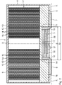
- a composite capacitor component 1 has an electrolytic capacitor 2 and a ceramic capacitor 3, which are connected in parallel.
- the electrolytic capacitor 2 and the ceramic capacitor 3 are arranged in a housing 4 which has an opening 5 on an underside.
- the housing 4 is designed as a hollow cylinder.
- the winding 9 is thus arranged such that the winding axis 8 intersects the contacting plane K.
- the electrolytic capacitor connections 10, 11 emerge from the winding 9 on one side which faces the contacting plane K.
- a seal 16 is arranged in the housing 4 between the winding 9 and the connection contacts 6, 7 and separates the winding 9 from the ceramic capacitor 3 and the connection contacts 6, 7.
- the seal 16 is made of a rubber material, for example.
- the seal 16 has a recess 17 in which the ceramic capacitor 3 is arranged.
- the recess 17 is arranged essentially centrally to the winding axis 8.
- the ceramic capacitor 3 is thus arranged between the electrolytic capacitor 2 and the contacting plane K.
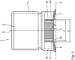
- the electrolytic capacitor connections 10, 11 emerge from the winding 9 at a distance D from one another.
- the electrolytic capacitor connections 10, 11 run outside of the winding 9 essentially parallel to one another and parallel to the winding axis 8.
- the ceramic capacitor 3 is arranged between the electrolytic capacitor connections 10, 11 when viewed parallel to the contacting plane K.
- the ceramic capacitor 3 has a first ceramic capacitor connection 18 and a second ceramic capacitor connection 19, which are arranged laterally on the ceramic capacitor 3 and one - parallel to the contact plane K considered - define dimension d.
- the first electrolytic capacitor connection 10 penetrates the seal 16 and is directly connected to the ceramic capacitor connection 18 and / or directly to the connection contact 6.
- the second electrolytic capacitor connection 11 penetrates the seal 16 and is connected directly to the second ceramic capacitor connection 19 and / or directly to the second connection contact 7.
- the first ceramic capacitor connection 18 is integrally connected to the first connection contact 6, so that they together have an L-shape.
- the second ceramic capacitor connection 19 is integrally connected to the second connection contact 7, so that these have an L-shape.
- the ceramic capacitor 3 has a plurality of first electrodes 20 which are connected to the first ceramic capacitor terminal 18 and are separated by a ceramic dielectric 21 from a plurality of second electrodes 22 which are connected to the second ceramic capacitor terminal 19.
- the electrolytic capacitor 2 has a capacitance C E , a parasitic series resistance ESR E and a parasitic series inductance ESL E.
- the ceramic capacitor 3 has a capacitance C K , a parasitic series resistance ESR K and a parasitic series inductance ESL K.
- the equivalent circuit diagram of the parallel connection of the electrolytic capacitor 2 and the ceramic capacitor 3 is shown in Fig. 3 illustrated. The resistances for the respective leakage current are shown in the equivalent circuit diagram in Fig. 3 neglected.
- the line lengths of the connecting lines are comparatively short, see above that the natural resonance frequencies SRF E and SRF K are increased and below the natural resonance frequencies SRF E and SRF K a comparatively larger operating frequency range ⁇ F is available.
- the operating frequency range ⁇ F both the electrolytic capacitor 2 and the ceramic capacitor 3 behave capacitively.
- the comparatively short connecting lines increase the natural resonance frequency SRF E of the electrolytic capacitor 2, so that the lower natural resonance frequency SRF E of the electrolytic capacitor 2 is matched to the higher natural resonance frequency SRF K of the ceramic capacitor 3.
- the natural resonance frequencies SRF E and SRF K can be matched to one another in the desired manner by choosing the capacitances C E and C K.
- Fig. 4 an amount of the impedances of the electrolytic capacitor 2 and the ceramic capacitor 3 as a function of the frequency f is shown qualitatively.
- the frequency f and the magnitude of the impedances are plotted logarithmically on the abscissa and ordinate. Because the natural resonance frequencies SRF E and SRF K are shifted to comparatively higher frequencies f, the comparatively larger operating frequency range ⁇ F is available. In addition, the frequency range between the natural resonance frequencies SRF E and SRF K is comparatively small, so that a parallel resonance and an excessive impedance of the parallel connection of the electrolytic capacitor 2 and the ceramic capacitor 3 in this frequency range are effectively avoided.
- the capacitor composite component 1 can be easily, flexibly and reliably integrated into an electronic circuit.
- the first electrolytic capacitor connection 10 is designed in one piece with the first connection contact 6, which together form an L-shape.
- the second electrolytic capacitor connection 11 is formed in one piece with the second connection contact 7, which together form an L-shape.
- the electrolytic capacitor 2 is designed, for example, as a polymer electrolytic capacitor.
- the electrolytic capacitor 2 has a higher capacitance than the ceramic capacitor 3.
- the capacitance C E of the electrolytic capacitor 2 can be up to 1000 ⁇ F, in particular up to 3000 ⁇ F and in particular up to 5000 ⁇ F.
- the capacitance C K of the ceramic capacitor can be 3 to 100 ⁇ F, in particular up to 300 ⁇ F, and in particular up to 500 ⁇ F.
- the composite capacitor component 1 has a low impedance even at comparatively high frequencies f and thus enables high interference suppression of switching pulses when the composite capacitor component 1 is used in an electronic circuit.
- the composite capacitor component 1 can be integrated into an electronic circuit in a simple, flexible and reliable manner and for mounting a printed circuit board or board can be used.
- the composite capacitor component 1 enables, for example, a switching regulator to have a low impedance over the entire frequency range, so that load changes can be buffered and interference from the switching pulses can be suppressed. The same applies to switching converters and other applications that require a charge buffer for load jumps and must prevent high-frequency switching pulses from spreading. Because the ceramic capacitor 3 is arranged between the electrolytic capacitor connections 10, 11, the connecting lines are short.
- the capacitor composite component 1 Since the parasitic series resistance ESR K of the ceramic capacitor 3 is much lower than the parasitic series resistance ESR E of the electrolytic capacitor 2 and the ceramic capacitor 3 has a better high-frequency behavior or a lower impedance at high frequencies, the capacitor composite component 1 has an improved EMC Behavior (EMC: electromagnetic compatibility).
- EMC electromagnetic compatibility
Landscapes
- Engineering & Computer Science (AREA)
- Power Engineering (AREA)
- Microelectronics & Electronic Packaging (AREA)
- Manufacturing & Machinery (AREA)
- Fixed Capacitors And Capacitor Manufacturing Machines (AREA)
- Structures For Mounting Electric Components On Printed Circuit Boards (AREA)
Claims (9)
- Composant composite de condensateur comprenant- un boîtier (4),- deux contacts de raccordement (6, 7), qui définissent un plan d'établissement de contact (K),- un condensateur électrolytique (2),-- qui comprend une bobine (9) et deux bornes de condensateur électrolytique (10, 11),-- qui est relié de manière électroconductrice aux contacts de raccordement (6, 7),- un condensateur en céramique (3),-- qui est branché en parallèle par rapport au condensateur électrolytique (2) et est relié de manière électroconductrice aux contacts de raccordement (6, 7),-- qui est disposé entre le condensateur électrolytique (2) et le plan d'établissement de contact (K),-- qui est disposé entre les bornes de condensateur électrolytique (10, 11),dans lequel le condensateur électrolytique (2) et le condensateur en céramique (3) sont disposés dans le boîtier (4),
caractérisé en ce
que le condensateur électrolytique (2) et le condensateur en céramique (3) sont séparés par une étanchéification (16),
que l'étanchéification (16) est disposée dans le boîtier (4),
que l'étanchéification (16) présente un évidement (17), dans lequel est disposé le condensateur en céramique (3). - Composant composite de condensateur selon la revendication 1, caractérisé en ce
que la bobine (9) définit un axe de bobine (8), qui coupe le plan d'établissement de contact (K). - Composant composite de condensateur selon la revendication 1 ou 2, caractérisé en ce
que la bobine (9) définit un axe de bobine (8), qui forme avec le plan d'établissement de contact (K) un angle a, dans lequel s'applique : 45° ≤ α ≤ 135°, en particulier 60° ≤ α ≤ 120°, et en particulier 75° ≤ α ≤ 105°. - Composant composite de condensateur selon l'une quelconque des revendications 1 à 3,
caractérisé en ce
que les bornes de condensateur électrolytique (10, 11) sortent au niveau d'un côté de la bobine (9), qui est tourné vers le plan d'établissement de contact (K). - Composant composite de condensateur selon l'une quelconque des revendications 1 à 4,
caractérisé en ce
que les bornes de condensateur électrolytique (10, 11) ont les unes des autres une distance D et le condensateur en céramique (3) a en parallèle par rapport au plan d'établissement de contact (K) une dimension d, dans lequel s'applique : 0,7 ≤ d/D ≤ 1,3, en particulier 0,8 ≤ d/D ≤ 1,2, et en particulier 0,9 ≤ d/D ≤ 1,1. - Composant composite de condensateur selon l'une quelconque des revendications 1 à 5, caractérisé en ce
que deux bornes de condensateur en céramique (18, 19) sont réalisées de manière latérale au niveau du condensateur en céramique (3). - Composant composite de condensateur selon l'une quelconque des revendications 1 à 6,
caractérisé en ce
que le condensateur en céramique (3) présente deux bornes de condensateur en céramique (18, 19), qui sont réalisées respectivement en une partie avec un des contacts de raccordement (6, 7). - Composant composite de condensateur selon l'une quelconque des revendications 1 à 6,
caractérisé en ce
que les bornes de condensateur électrolytique (10, 11) sont réalisées respectivement d'un seul tenant avec un des contacts de raccordement (6, 7). - Composant composite de condensateur selon l'une quelconque des revendications 1 à 8,
caractérisé en ce
que le condensateur électrolytique (2) a une première fréquence de résonance propre SRFE et le condensateur en céramique (3) a une deuxième fréquence de résonance propre SRFK, dans lequel s'applique : 0,7 ≤ SRFE/SRFK ≤ 1,3, en particulier 0,8 ≤ SRFE/SRFK ≤ 1,2, et en particulier 0,9 ≤ SRFE/SRFK ≤ 1,1.
Applications Claiming Priority (2)
| Application Number | Priority Date | Filing Date | Title |
|---|---|---|---|
| DE102018208743.1A DE102018208743A1 (de) | 2018-06-04 | 2018-06-04 | Kondensator-Verbund-Bauteil |
| PCT/EP2019/063810 WO2019233825A1 (fr) | 2018-06-04 | 2019-05-28 | Élément composite de condensateur |
Publications (2)
| Publication Number | Publication Date |
|---|---|
| EP3662491A1 EP3662491A1 (fr) | 2020-06-10 |
| EP3662491B1 true EP3662491B1 (fr) | 2020-11-18 |
Family
ID=66752076
Family Applications (1)
| Application Number | Title | Priority Date | Filing Date |
|---|---|---|---|
| EP19728368.2A Active EP3662491B1 (fr) | 2018-06-04 | 2019-05-28 | Composant capacitif composite |
Country Status (4)
| Country | Link |
|---|---|
| EP (1) | EP3662491B1 (fr) |
| DE (1) | DE102018208743A1 (fr) |
| TW (1) | TWI693619B (fr) |
| WO (1) | WO2019233825A1 (fr) |
Family Cites Families (9)
| Publication number | Priority date | Publication date | Assignee | Title |
|---|---|---|---|---|
| JPS5547718U (fr) * | 1978-09-21 | 1980-03-28 | ||
| JPH0191411A (ja) * | 1987-10-02 | 1989-04-11 | Hitachi Condenser Co Ltd | 複合コンデンサ |
| JPH01109711A (ja) * | 1987-10-23 | 1989-04-26 | Matsushita Electric Ind Co Ltd | 複合チップ状固体電解コンデンサ |
| JPH09326334A (ja) * | 1996-06-04 | 1997-12-16 | Murata Mfg Co Ltd | タンタル・セラミック複合コンデンサ |
| JP2003234246A (ja) * | 2002-02-07 | 2003-08-22 | Sony Corp | 複合コンデンサ |
| US20160020024A1 (en) * | 2014-07-18 | 2016-01-21 | Samsung Electro-Mechanics Co., Ltd. | Composite electronic component and board having the same |
| KR102183426B1 (ko) | 2015-07-17 | 2020-11-26 | 삼성전기주식회사 | 복합 전자부품 및 그 실장 기판 |
| KR102202471B1 (ko) * | 2015-11-25 | 2021-01-13 | 삼성전기주식회사 | 복합 전자 부품 및 그 실장 기판 |
| JP2017199867A (ja) * | 2016-04-28 | 2017-11-02 | 株式会社ジェイテクト | 複合コンデンサ |
-
2018
- 2018-06-04 DE DE102018208743.1A patent/DE102018208743A1/de not_active Withdrawn
-
2019
- 2019-05-28 EP EP19728368.2A patent/EP3662491B1/fr active Active
- 2019-05-28 WO PCT/EP2019/063810 patent/WO2019233825A1/fr not_active Ceased
- 2019-06-03 TW TW108119223A patent/TWI693619B/zh active
Non-Patent Citations (1)
| Title |
|---|
| None * |
Also Published As
| Publication number | Publication date |
|---|---|
| TWI693619B (zh) | 2020-05-11 |
| EP3662491A1 (fr) | 2020-06-10 |
| TW202004795A (zh) | 2020-01-16 |
| WO2019233825A1 (fr) | 2019-12-12 |
| DE102018208743A1 (de) | 2019-12-05 |
Similar Documents
| Publication | Publication Date | Title |
|---|---|---|
| DE102010031416B4 (de) | Kartenrandverbinder und Verfahren zu dessen Fertigung | |
| DE69012914T2 (de) | Verfahren zur Herstellung eines elektrischen Verbinders mit Filter. | |
| EP1350257B1 (fr) | Composant multicouche electrique et circuit antiparasites pourvu d'un tel composant | |
| EP3642858B1 (fr) | Condensateur de circuit intermédiaire | |
| DE102010029682A1 (de) | Kartenrandverbinder und Verfahren für dessen Zusammenbau | |
| DE10218295A1 (de) | Kondensatormodul und Kondensatorbatterie mit dem Kondensatormodul | |
| WO2000031837A1 (fr) | Dispositif de blindage pour plaquettes a bornes utilisees dans le domaine des telecommunications et de l'informatique | |
| WO2014139696A1 (fr) | Composant électronique | |
| WO2024165263A1 (fr) | Dispositif de connexion de fiche de charge | |
| WO2018219919A1 (fr) | Dispositif pour réduire des tensions de palier préjudiciables | |
| EP3662491B1 (fr) | Composant capacitif composite | |
| EP3482465B1 (fr) | Élément de contact à conducteur interne, sollicité par un ressort | |
| DE102019208778A1 (de) | Einpressanschluss und Substratanordnung | |
| EP3987557B1 (fr) | Composante inductive | |
| EP1709696B1 (fr) | Actionneur piezoelectrique | |
| EP3906571A1 (fr) | Composant inductif | |
| DE202019106744U1 (de) | Entstörfilter | |
| DE102015117452A1 (de) | Folienkondensator und Verfahren zur Herstellung eines Folienkondensators | |
| DE102008054675A1 (de) | Elektrischer Steckverbinder sowie Verfahren zum Montieren eines elektrischen Kabels im elektrischen Steckverbinder | |
| EP4133511B1 (fr) | Condensateurs à film | |
| DE102019127686B4 (de) | Durchführung für eine elektrische Heizvorrichtung, elektrische Heizvorrichtung mit einer solchen Durchführung, System mit einer solchen Durchführung und Verfahren zur Herstellung einer solchen Durchführung | |
| DE102009001416A1 (de) | Entstörvorrichtung sowie Verfahren zur Herstellung | |
| DE102004036431B4 (de) | Elektrischer Keramikkondensator | |
| EP3482461A1 (fr) | Dispositif de contact électrique | |
| DE202017103248U1 (de) | Vorrichtung zur Reduzierung von schädlichen Lagerspannungen |
Legal Events
| Date | Code | Title | Description |
|---|---|---|---|
| STAA | Information on the status of an ep patent application or granted ep patent |
Free format text: STATUS: UNKNOWN |
|
| STAA | Information on the status of an ep patent application or granted ep patent |
Free format text: STATUS: THE INTERNATIONAL PUBLICATION HAS BEEN MADE |
|
| PUAI | Public reference made under article 153(3) epc to a published international application that has entered the european phase |
Free format text: ORIGINAL CODE: 0009012 |
|
| STAA | Information on the status of an ep patent application or granted ep patent |
Free format text: STATUS: REQUEST FOR EXAMINATION WAS MADE |
|
| 17P | Request for examination filed |
Effective date: 20200305 |
|
| AK | Designated contracting states |
Kind code of ref document: A1 Designated state(s): AL AT BE BG CH CY CZ DE DK EE ES FI FR GB GR HR HU IE IS IT LI LT LU LV MC MK MT NL NO PL PT RO RS SE SI SK SM TR |
|
| AX | Request for extension of the european patent |
Extension state: BA ME |
|
| GRAP | Despatch of communication of intention to grant a patent |
Free format text: ORIGINAL CODE: EPIDOSNIGR1 |
|
| STAA | Information on the status of an ep patent application or granted ep patent |
Free format text: STATUS: GRANT OF PATENT IS INTENDED |
|
| DAV | Request for validation of the european patent (deleted) | ||
| DAX | Request for extension of the european patent (deleted) | ||
| INTG | Intention to grant announced |
Effective date: 20200813 |
|
| GRAS | Grant fee paid |
Free format text: ORIGINAL CODE: EPIDOSNIGR3 |
|
| GRAA | (expected) grant |
Free format text: ORIGINAL CODE: 0009210 |
|
| STAA | Information on the status of an ep patent application or granted ep patent |
Free format text: STATUS: THE PATENT HAS BEEN GRANTED |
|
| AK | Designated contracting states |
Kind code of ref document: B1 Designated state(s): AL AT BE BG CH CY CZ DE DK EE ES FI FR GB GR HR HU IE IS IT LI LT LU LV MC MK MT NL NO PL PT RO RS SE SI SK SM TR |
|
| REG | Reference to a national code |
Ref country code: GB Ref legal event code: FG4D Free format text: NOT ENGLISH |
|
| REG | Reference to a national code |
Ref country code: CH Ref legal event code: EP |
|
| REG | Reference to a national code |
Ref country code: IE Ref legal event code: FG4D Free format text: LANGUAGE OF EP DOCUMENT: GERMAN |
|
| REG | Reference to a national code |
Ref country code: DE Ref legal event code: R096 Ref document number: 502019000427 Country of ref document: DE |
|
| REG | Reference to a national code |
Ref country code: AT Ref legal event code: REF Ref document number: 1336666 Country of ref document: AT Kind code of ref document: T Effective date: 20201215 |
|
| REG | Reference to a national code |
Ref country code: NL Ref legal event code: MP Effective date: 20201118 |
|
| PG25 | Lapsed in a contracting state [announced via postgrant information from national office to epo] |
Ref country code: FI Free format text: LAPSE BECAUSE OF FAILURE TO SUBMIT A TRANSLATION OF THE DESCRIPTION OR TO PAY THE FEE WITHIN THE PRESCRIBED TIME-LIMIT Effective date: 20201118 Ref country code: RS Free format text: LAPSE BECAUSE OF FAILURE TO SUBMIT A TRANSLATION OF THE DESCRIPTION OR TO PAY THE FEE WITHIN THE PRESCRIBED TIME-LIMIT Effective date: 20201118 Ref country code: PT Free format text: LAPSE BECAUSE OF FAILURE TO SUBMIT A TRANSLATION OF THE DESCRIPTION OR TO PAY THE FEE WITHIN THE PRESCRIBED TIME-LIMIT Effective date: 20210318 Ref country code: GR Free format text: LAPSE BECAUSE OF FAILURE TO SUBMIT A TRANSLATION OF THE DESCRIPTION OR TO PAY THE FEE WITHIN THE PRESCRIBED TIME-LIMIT Effective date: 20210219 Ref country code: NO Free format text: LAPSE BECAUSE OF FAILURE TO SUBMIT A TRANSLATION OF THE DESCRIPTION OR TO PAY THE FEE WITHIN THE PRESCRIBED TIME-LIMIT Effective date: 20210218 |
|
| PG25 | Lapsed in a contracting state [announced via postgrant information from national office to epo] |
Ref country code: PL Free format text: LAPSE BECAUSE OF FAILURE TO SUBMIT A TRANSLATION OF THE DESCRIPTION OR TO PAY THE FEE WITHIN THE PRESCRIBED TIME-LIMIT Effective date: 20201118 Ref country code: LV Free format text: LAPSE BECAUSE OF FAILURE TO SUBMIT A TRANSLATION OF THE DESCRIPTION OR TO PAY THE FEE WITHIN THE PRESCRIBED TIME-LIMIT Effective date: 20201118 Ref country code: IS Free format text: LAPSE BECAUSE OF FAILURE TO SUBMIT A TRANSLATION OF THE DESCRIPTION OR TO PAY THE FEE WITHIN THE PRESCRIBED TIME-LIMIT Effective date: 20210318 Ref country code: SE Free format text: LAPSE BECAUSE OF FAILURE TO SUBMIT A TRANSLATION OF THE DESCRIPTION OR TO PAY THE FEE WITHIN THE PRESCRIBED TIME-LIMIT Effective date: 20201118 Ref country code: BG Free format text: LAPSE BECAUSE OF FAILURE TO SUBMIT A TRANSLATION OF THE DESCRIPTION OR TO PAY THE FEE WITHIN THE PRESCRIBED TIME-LIMIT Effective date: 20210218 |
|
| REG | Reference to a national code |
Ref country code: LT Ref legal event code: MG9D |
|
| PG25 | Lapsed in a contracting state [announced via postgrant information from national office to epo] |
Ref country code: HR Free format text: LAPSE BECAUSE OF FAILURE TO SUBMIT A TRANSLATION OF THE DESCRIPTION OR TO PAY THE FEE WITHIN THE PRESCRIBED TIME-LIMIT Effective date: 20201118 |
|
| PG25 | Lapsed in a contracting state [announced via postgrant information from national office to epo] |
Ref country code: RO Free format text: LAPSE BECAUSE OF FAILURE TO SUBMIT A TRANSLATION OF THE DESCRIPTION OR TO PAY THE FEE WITHIN THE PRESCRIBED TIME-LIMIT Effective date: 20201118 Ref country code: LT Free format text: LAPSE BECAUSE OF FAILURE TO SUBMIT A TRANSLATION OF THE DESCRIPTION OR TO PAY THE FEE WITHIN THE PRESCRIBED TIME-LIMIT Effective date: 20201118 Ref country code: CZ Free format text: LAPSE BECAUSE OF FAILURE TO SUBMIT A TRANSLATION OF THE DESCRIPTION OR TO PAY THE FEE WITHIN THE PRESCRIBED TIME-LIMIT Effective date: 20201118 Ref country code: EE Free format text: LAPSE BECAUSE OF FAILURE TO SUBMIT A TRANSLATION OF THE DESCRIPTION OR TO PAY THE FEE WITHIN THE PRESCRIBED TIME-LIMIT Effective date: 20201118 Ref country code: SM Free format text: LAPSE BECAUSE OF FAILURE TO SUBMIT A TRANSLATION OF THE DESCRIPTION OR TO PAY THE FEE WITHIN THE PRESCRIBED TIME-LIMIT Effective date: 20201118 Ref country code: SK Free format text: LAPSE BECAUSE OF FAILURE TO SUBMIT A TRANSLATION OF THE DESCRIPTION OR TO PAY THE FEE WITHIN THE PRESCRIBED TIME-LIMIT Effective date: 20201118 |
|
| REG | Reference to a national code |
Ref country code: DE Ref legal event code: R097 Ref document number: 502019000427 Country of ref document: DE |
|
| PG25 | Lapsed in a contracting state [announced via postgrant information from national office to epo] |
Ref country code: DK Free format text: LAPSE BECAUSE OF FAILURE TO SUBMIT A TRANSLATION OF THE DESCRIPTION OR TO PAY THE FEE WITHIN THE PRESCRIBED TIME-LIMIT Effective date: 20201118 |
|
| PLBE | No opposition filed within time limit |
Free format text: ORIGINAL CODE: 0009261 |
|
| STAA | Information on the status of an ep patent application or granted ep patent |
Free format text: STATUS: NO OPPOSITION FILED WITHIN TIME LIMIT |
|
| 26N | No opposition filed |
Effective date: 20210819 |
|
| PG25 | Lapsed in a contracting state [announced via postgrant information from national office to epo] |
Ref country code: NL Free format text: LAPSE BECAUSE OF FAILURE TO SUBMIT A TRANSLATION OF THE DESCRIPTION OR TO PAY THE FEE WITHIN THE PRESCRIBED TIME-LIMIT Effective date: 20201118 Ref country code: AL Free format text: LAPSE BECAUSE OF FAILURE TO SUBMIT A TRANSLATION OF THE DESCRIPTION OR TO PAY THE FEE WITHIN THE PRESCRIBED TIME-LIMIT Effective date: 20201118 Ref country code: IT Free format text: LAPSE BECAUSE OF FAILURE TO SUBMIT A TRANSLATION OF THE DESCRIPTION OR TO PAY THE FEE WITHIN THE PRESCRIBED TIME-LIMIT Effective date: 20201118 |
|
| PG25 | Lapsed in a contracting state [announced via postgrant information from national office to epo] |
Ref country code: SI Free format text: LAPSE BECAUSE OF FAILURE TO SUBMIT A TRANSLATION OF THE DESCRIPTION OR TO PAY THE FEE WITHIN THE PRESCRIBED TIME-LIMIT Effective date: 20201118 |
|
| PG25 | Lapsed in a contracting state [announced via postgrant information from national office to epo] |
Ref country code: MC Free format text: LAPSE BECAUSE OF FAILURE TO SUBMIT A TRANSLATION OF THE DESCRIPTION OR TO PAY THE FEE WITHIN THE PRESCRIBED TIME-LIMIT Effective date: 20201118 Ref country code: ES Free format text: LAPSE BECAUSE OF FAILURE TO SUBMIT A TRANSLATION OF THE DESCRIPTION OR TO PAY THE FEE WITHIN THE PRESCRIBED TIME-LIMIT Effective date: 20201118 Ref country code: LU Free format text: LAPSE BECAUSE OF NON-PAYMENT OF DUE FEES Effective date: 20210528 |
|
| REG | Reference to a national code |
Ref country code: BE Ref legal event code: MM Effective date: 20210531 |
|
| PG25 | Lapsed in a contracting state [announced via postgrant information from national office to epo] |
Ref country code: IE Free format text: LAPSE BECAUSE OF NON-PAYMENT OF DUE FEES Effective date: 20210528 |
|
| PG25 | Lapsed in a contracting state [announced via postgrant information from national office to epo] |
Ref country code: IS Free format text: LAPSE BECAUSE OF FAILURE TO SUBMIT A TRANSLATION OF THE DESCRIPTION OR TO PAY THE FEE WITHIN THE PRESCRIBED TIME-LIMIT Effective date: 20210318 |
|
| PG25 | Lapsed in a contracting state [announced via postgrant information from national office to epo] |
Ref country code: BE Free format text: LAPSE BECAUSE OF NON-PAYMENT OF DUE FEES Effective date: 20210531 |
|
| REG | Reference to a national code |
Ref country code: CH Ref legal event code: PL |
|
| PG25 | Lapsed in a contracting state [announced via postgrant information from national office to epo] |
Ref country code: LI Free format text: LAPSE BECAUSE OF NON-PAYMENT OF DUE FEES Effective date: 20220531 Ref country code: CH Free format text: LAPSE BECAUSE OF NON-PAYMENT OF DUE FEES Effective date: 20220531 |
|
| P01 | Opt-out of the competence of the unified patent court (upc) registered |
Effective date: 20230517 |
|
| PG25 | Lapsed in a contracting state [announced via postgrant information from national office to epo] |
Ref country code: CY Free format text: LAPSE BECAUSE OF FAILURE TO SUBMIT A TRANSLATION OF THE DESCRIPTION OR TO PAY THE FEE WITHIN THE PRESCRIBED TIME-LIMIT Effective date: 20201118 |
|
| PG25 | Lapsed in a contracting state [announced via postgrant information from national office to epo] |
Ref country code: HU Free format text: LAPSE BECAUSE OF FAILURE TO SUBMIT A TRANSLATION OF THE DESCRIPTION OR TO PAY THE FEE WITHIN THE PRESCRIBED TIME-LIMIT; INVALID AB INITIO Effective date: 20190528 |
|
| PG25 | Lapsed in a contracting state [announced via postgrant information from national office to epo] |
Ref country code: MK Free format text: LAPSE BECAUSE OF FAILURE TO SUBMIT A TRANSLATION OF THE DESCRIPTION OR TO PAY THE FEE WITHIN THE PRESCRIBED TIME-LIMIT Effective date: 20201118 |
|
| PG25 | Lapsed in a contracting state [announced via postgrant information from national office to epo] |
Ref country code: MT Free format text: LAPSE BECAUSE OF FAILURE TO SUBMIT A TRANSLATION OF THE DESCRIPTION OR TO PAY THE FEE WITHIN THE PRESCRIBED TIME-LIMIT Effective date: 20201118 |
|
| PGFP | Annual fee paid to national office [announced via postgrant information from national office to epo] |
Ref country code: DE Payment date: 20250521 Year of fee payment: 7 |
|
| PGFP | Annual fee paid to national office [announced via postgrant information from national office to epo] |
Ref country code: GB Payment date: 20250527 Year of fee payment: 7 |
|
| REG | Reference to a national code |
Ref country code: AT Ref legal event code: MM01 Ref document number: 1336666 Country of ref document: AT Kind code of ref document: T Effective date: 20240528 |
|
| PGFP | Annual fee paid to national office [announced via postgrant information from national office to epo] |
Ref country code: FR Payment date: 20250528 Year of fee payment: 7 |
|
| PG25 | Lapsed in a contracting state [announced via postgrant information from national office to epo] |
Ref country code: AT Free format text: LAPSE BECAUSE OF NON-PAYMENT OF DUE FEES Effective date: 20240528 |
|
| PG25 | Lapsed in a contracting state [announced via postgrant information from national office to epo] |
Ref country code: TR Free format text: LAPSE BECAUSE OF FAILURE TO SUBMIT A TRANSLATION OF THE DESCRIPTION OR TO PAY THE FEE WITHIN THE PRESCRIBED TIME-LIMIT Effective date: 20201118 |
|
| PGFP | Annual fee paid to national office [announced via postgrant information from national office to epo] |
Ref country code: AT Payment date: 20260410 Year of fee payment: 5 |