EP3661014A1 - Amélioration de la détection des corps étrangers grâce à la détection du courant de bobine dans les systèmes de transfert d'énergie sans fil - Google Patents
Amélioration de la détection des corps étrangers grâce à la détection du courant de bobine dans les systèmes de transfert d'énergie sans fil Download PDFInfo
- Publication number
- EP3661014A1 EP3661014A1 EP19211875.0A EP19211875A EP3661014A1 EP 3661014 A1 EP3661014 A1 EP 3661014A1 EP 19211875 A EP19211875 A EP 19211875A EP 3661014 A1 EP3661014 A1 EP 3661014A1
- Authority
- EP
- European Patent Office
- Prior art keywords
- coil
- coil current
- current
- transmitter
- peak
- Prior art date
- Legal status (The legal status is an assumption and is not a legal conclusion. Google has not performed a legal analysis and makes no representation as to the accuracy of the status listed.)
- Granted
Links
- 238000012546 transfer Methods 0.000 title claims abstract description 27
- 238000001514 detection method Methods 0.000 title claims abstract description 10
- 238000000034 method Methods 0.000 claims description 16
- 239000003990 capacitor Substances 0.000 claims description 12
- 238000012935 Averaging Methods 0.000 claims description 9
- 238000010586 diagram Methods 0.000 description 33
- 238000005259 measurement Methods 0.000 description 16
- 238000005070 sampling Methods 0.000 description 14
- 230000005540 biological transmission Effects 0.000 description 12
- 238000002307 isotope ratio mass spectrometry Methods 0.000 description 5
- 238000004364 calculation method Methods 0.000 description 3
- 238000010438 heat treatment Methods 0.000 description 3
- 238000013213 extrapolation Methods 0.000 description 2
- 239000002184 metal Substances 0.000 description 2
- 101710096660 Probable acetoacetate decarboxylase 2 Proteins 0.000 description 1
- 238000010521 absorption reaction Methods 0.000 description 1
- 230000000903 blocking effect Effects 0.000 description 1
- 230000003139 buffering effect Effects 0.000 description 1
- 238000004891 communication Methods 0.000 description 1
- 230000007423 decrease Effects 0.000 description 1
- 239000000284 extract Substances 0.000 description 1
- 238000001914 filtration Methods 0.000 description 1
- 231100001261 hazardous Toxicity 0.000 description 1
- 238000000691 measurement method Methods 0.000 description 1
- 238000012986 modification Methods 0.000 description 1
- 230000004048 modification Effects 0.000 description 1
- 230000000717 retained effect Effects 0.000 description 1
- 238000009420 retrofitting Methods 0.000 description 1
Images


Classifications
-
- H—ELECTRICITY
- H02—GENERATION; CONVERSION OR DISTRIBUTION OF ELECTRIC POWER
- H02J—CIRCUIT ARRANGEMENTS OR SYSTEMS FOR SUPPLYING OR DISTRIBUTING ELECTRIC POWER; SYSTEMS FOR STORING ELECTRIC ENERGY
- H02J50/00—Circuit arrangements or systems for wireless supply or distribution of electric power
- H02J50/60—Circuit arrangements or systems for wireless supply or distribution of electric power responsive to the presence of foreign objects, e.g. detection of living beings
-
- G—PHYSICS
- G01—MEASURING; TESTING
- G01V—GEOPHYSICS; GRAVITATIONAL MEASUREMENTS; DETECTING MASSES OR OBJECTS; TAGS
- G01V3/00—Electric or magnetic prospecting or detecting; Measuring magnetic field characteristics of the earth, e.g. declination, deviation
- G01V3/08—Electric or magnetic prospecting or detecting; Measuring magnetic field characteristics of the earth, e.g. declination, deviation operating with magnetic or electric fields produced or modified by objects or geological structures or by detecting devices
- G01V3/10—Electric or magnetic prospecting or detecting; Measuring magnetic field characteristics of the earth, e.g. declination, deviation operating with magnetic or electric fields produced or modified by objects or geological structures or by detecting devices using induction coils
-
- H—ELECTRICITY
- H02—GENERATION; CONVERSION OR DISTRIBUTION OF ELECTRIC POWER
- H02J—CIRCUIT ARRANGEMENTS OR SYSTEMS FOR SUPPLYING OR DISTRIBUTING ELECTRIC POWER; SYSTEMS FOR STORING ELECTRIC ENERGY
- H02J50/00—Circuit arrangements or systems for wireless supply or distribution of electric power
- H02J50/10—Circuit arrangements or systems for wireless supply or distribution of electric power using inductive coupling
- H02J50/12—Circuit arrangements or systems for wireless supply or distribution of electric power using inductive coupling of the resonant type
-
- H—ELECTRICITY
- H02—GENERATION; CONVERSION OR DISTRIBUTION OF ELECTRIC POWER
- H02J—CIRCUIT ARRANGEMENTS OR SYSTEMS FOR SUPPLYING OR DISTRIBUTING ELECTRIC POWER; SYSTEMS FOR STORING ELECTRIC ENERGY
- H02J50/00—Circuit arrangements or systems for wireless supply or distribution of electric power
- H02J50/40—Circuit arrangements or systems for wireless supply or distribution of electric power using two or more transmitting or receiving devices
- H02J50/402—Circuit arrangements or systems for wireless supply or distribution of electric power using two or more transmitting or receiving devices the two or more transmitting or the two or more receiving devices being integrated in the same unit, e.g. power mats with several coils or antennas with several sub-antennas
Definitions
- Embodiments of the present invention are related wireless power transfer and more particularly to enhanced foreign object detection with coil current sensing in wireless power transfer systems.
- Wireless power transfer is the transmission of electrical energy without wires as a physical link.
- a transmitter device driven by electric power from a power source, generates a time-varying electromagnetic or magnetic field, which transmits power across space to a receiver device, which extracts power from the field and supplies it to an electrical load.
- Wireless power transfer is useful to power electrical devices where interconnecting wires are inconvenient, hazardous, or are not possible.
- the transmitter circuit is usually built on an integrated circuit (IC) chip.
- a wireless power transmitter that includes one transmitter IC chip can only be used to charge one wireless power receiving device at a time.
- multiple wireless chargers are usually used if more than one wireless devices are to be charged at the same time.
- the cost of obtaining a number of wireless chargers can be significant.
- foreign object detection (FOD) is continuously a problem for such systems.
- a foreign object can appear at any time during the transfer of wireless power between the transmitter and the receiver. The presence of a foreign object not only affects the efficiency of the wireless power transfer, but also the foreign object can be subject to excessive heating that can become dangerous.
- FOD foreign object detection
- the method includes determining, via a coil current sensing circuit at the wireless power transmitting device, a coil current value corresponding to a first coil current that passes through a first transmitter coil.
- the method further comprises computing, via a controller at the wireless power transmitting device, a transmitter power loss based on the coil current value.
- the method further comprises determining, during wireless power transfer from the wireless power transmitting device to a wireless power receiving device, an existence of a foreign object in vicinity of the first transmitter coil when a change in the computed transmitter power loss meets a threshold condition.
- Embodiments described herein further provide a wireless power transmitting device for foreign object detection based on coil current sensing.
- the wireless power transmitting device includes a transmitter coil, a coil current sensing circuit coupled to the transmitter coil, and a controller.
- the controller is configured to determine, via the coil current sensing circuit, a coil current value corresponding to a first coil current that passes through a first transmitter coil, compute a transmitter power loss based on the coil current value, and determine, during wireless power transfer from the wireless power transmitting device to a wireless power receiving device, an existence of a foreign object in vicinity of the first transmitter coil when a change in the computed transmitter power loss meets a threshold condition.
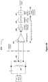
- FIG. 1 illustrates an example wireless power transmission system 100 that is configured to engage coil current sensing for a multi-coil transmitter, according to some embodiments.
- a power transmitter TX 102 is coupled to a power supply 112 that provides power to drive TX 102.
- the controller 107 of Tx 102 is configured to generate an alternate current (AC) through the one or more transmitter coils 106a, 106b, each of which produces a time varying magnetic field.
- AC alternate current
- Each of the time varying magnetic fields produced by the transmitter coils 106a and 106b induces a respective current in receiver coil 108a and 108b, respectively.
- Receiver coil 108a or 108b (herein collectively referred to as receiver coil 108) is coupled to a respective power receiver RX 104a or 104b (herein collectively referred to as receiver 104), respectively, each of which receives the transmitted wireless power.
- a rectifier circuit 110a or 110b (herein collectively referred to as rectifier 110) is within the receiving device 104a or104b, respectively, configured to receive and rectifies wireless power received at the receiver coil 108a or 108b, and then in turn provides an output voltage for battery charging.
- each of the receiver RX 104a and 104b is coupled to a load 114a or 114b, for example, a battery charger, which is configured to charge a battery with the received power.
- the load 114a and 114b can be charged with wireless power transferred from Tx 102 at the same time.
- the transmitting device 102 may have a larger active charging area and a receiving device can be placed with more freedom on the charging area to be charged.
- the Tx controller 107 can be built on a single IC chip. For the Tx 102 to charge more than one device at once, the controller 107 is configured to provide high power transfer of up to at least 20 W, authentication for safe high power wireless transfer.
- the controller 107 is configured to provide foreign object detection (FOD) via coil current sensing and increased X-Y placement ability for multiple receiving devices.
- FOD foreign object detection
- Figure 1 when a foreign object 124 is placed in vicinity to the transmitter coil 106a-b or receiver coil 108a-b, the foreign object 124 can interfere with the transmission of power between transmitting device 102 and receiving device(s) 104a-b.
- Figures 2A provide an example diagram illustrating the impact of a foreign object on the power loss of the wireless power transfer system 100 shown in Figure 1 , according to an embodiment.
- the transmitting device 102 finds the power loss P LOSS when a metal object 124 is placed in vicinity to the transmitter coil during the wireless power transfer, calculated as the difference between the transmitted power P PT from transmitter coil and the received power P PR received at the receiver coil. If P LOSS is big, then a foreign object issue exists.
- the transmitting device 102 calculates the input power P IN and the transmitter power loss P PTLoss and the receiving device 104 tells the transmitting device 102 the received power P PR , e.g., by sending a received power packet (RPP) 135 to transmitting device 102.
- RPP received power packet
- P PT Vin or VBRG ⁇ Iin ⁇ P PTLoss
- Vin denote the input voltage
- VBRG is the Bridge voltage applied to the the Tx DC to AC inverter to create the Tx magnetic field
- TX LOSSES denotes the power loss within the transmitting device 102, e.g., power consumed at the transmitter coil and electrical components necessary to create the Tx magnetic field.
- P PR the power received at the receiving device 104
- P PR the power received at the receiving device 104
- Vrect the voltage at the rectifier circuit 110 at receiving devices 104
- lout denotes the output charging current from the receiving device 104
- P PRLoss denotes the power loss within the receiving device 104.
- P PR is then communicated to transmitting device 102 via RPP 135.
- the average input current Iin and average input voltage Vin are measured, and then Tx LOSSES is calculated, e.g., via extrapolation.
- Integrated Circuits can be designed to directly measure the transmitter coil current.
- the measured transmitter coil current (RMS or peak current) and phase relative to Tx coil voltage provides an indicator of the transmitter coil losses, which is usually the major source of power loss in the transmitting device 102. Retrofitting this concept of transmitter coil current measurement into existing ICs can be challenging and costly.
- FIGS 2B-2C provide example data diagrams illustrating impacts of the alignment between the transmitting device 102 and the receiving device 104 on the power loss and coil current, according to some embodiments described herein.
- the transmitter coil current can vary with the position of the receiver coil 108 (of the receiving device 104).
- the transmitter power loss (reflected by the transmitter coil current PTx_coil_IRMS) may vary up to four times while the X-Y position of the receiving device varies, e.g., when the receiving device moves on the X-Y plane of the transmitter charging pad.
- the transmitter coil current may change from 2.6A to close to 5A while the Z-position (e.g., the direction vertical to the charging panel) of the transmitter coil changes relative to the receiver coil.
- Embodiments described herein provide a coil current sensing circuit to ICs with analog-to-digital converters (ADCs).
- the coil sensing circuit 125a-b may be placed internally to the transmitting device 102 to measure the coil current of the coils 106a-b.
- the coil sensing circuit 125a-b may be placed external to the IC of transmitting device 102, and is communicatively coupled to the coils 106a-b.
- the coil current sensing circuit is configured to measure a peak coil current value and the resonant frequency at the coil.
- the controller 107 then calculates a root mean square of the coil current for power loss calculation at transmitter coil 106a-b.
- the transmitter power loss computed directly based on the coil current (instead of the conventional computation based on transmitter input current) can provide improved precision of a change in the power loss.
- the computed power loss can be used to more accurately detect a foreign object near the transmitter coil during a wireless power transfer.
- the enhanced precision of power loss computation obviates or reduces the impact of X-Y position of the coils on FOD, and thus provides for enhanced X-Y freedom of charging placement.
- Figure 3 provide an example schematic circuit diagram 300 for a coil current sensing circuit (similar to 125a-b in Figure 1 ), according to embodiments described herein.
- the coil sensing circuit is coupled to transmitter coil 106, which is further coupled to resonance capacitors 144 (not shown).
- the coil sensing circuit obtains measurements such as an inductor alternate current resistance (ACR), the MOSFET drain-source on resistance (RDSON), i.e., the total resistance between the drain and source of the MOSFET, sensor resistance, and/or the like, and then measure the voltages across the inductor coil, the MOSFET, the sensor, and/or the like to monitor the coil current that passes through the Tx coil 106.
- ACR inductor alternate current resistance
- RDSON MOSFET drain-source on resistance
- L denotes the inductance of the coil 106
- R denotes the resistance of resistor (e.g., see R215) in the parallel RC circuit
- C denotes the capacitance of the capacitor (e.g., see C170) in the parallel RC circuit.
- the voltage (at node 146) across the capacitor C170 in the parallel resistor- RC circuit consisting of capacitor C170 and resistor R215 is sampled.
- the measured voltage at node 146 of the RC circuit is indicative of the coil current that passes through Tx coil 106.
- the low side MOSFET RDSON can be measured, or a sensing resistor (which may add additional component cost and power loss) can be used to measure the coil current, e.g., by measuring the voltage (at node 147) across the low-side MOSFET Q6 (as shown at circle 148 in diagram 300) divided by the MOSFET RDSON, or the voltage across the sensing resistor divided by the sensing resistance.
- An OPAMP shown at 127 in Figure 4 ) may be used help these measurements as such measurements can be 4 times lower than the ACR sensing.
- FIG 4A provides an example schematic circuit diagram 400 for an auto-selection circuit that selects a coil to monitor in a multi-coil transmitter, according to embodiments described herein.
- MOSFETs 117 and 118 are used to control which coil is to be measured.
- the MOSFETs 117 and 118 are each coupled to transmitter coils 106a or 106b, respectively, and are each tied to a dedicated gate signal that turns the MOSFET 117 or 118 on or off to automatically select which coil is being monitored.
- MOSFET 117 or 118 only becomes an active path when the respective gate signal is positive, and the respective coil 106a or 106b is energized.
- the voltage at node i_AC1 or i_AC2 is measured, respectively, to indicate the current of the respective coil coupled to MOSFET 117 or 118, e.g., by dividing the MOSFET RDSON of MOSFET 117 or 118.
- a parallel RC circuit (e.g., similar to c170 and R215 shown in Figure 3 ) is placed in parallel to the transmitters coil 106a or 106b such that the MOFSET 117 or 118 may sample the voltage at node 146a or 146b via parallel RC sensing.
- the sampled voltage of the parallel RC circuit is indicative of the coil current that passes through Tx coil 106a or 106b, respectively.
- diagram 400 shows two coils 106a-b and two MOSFETs 117-118 for automatically selecting the coil to be measured.
- Multiple coils e.g., more than two can be used in the transmitter.
- Each transmitter coil e.g., more than two
- Diagram 400 further includes an OPAMP 127 to amplify the signal from coil 106a or 106b before feeding to an analog-to-digital converter (ADC) that converts the analog current or voltage to a digital measurement to the processor (e.g., controller 107 in Figure 1 ).
- ADC analog-to-digital converter
- the OPAMP 127 provides improved signal-to-noise ratio (SNR) and additional buffering of the signal.
- Diagram 400 further shows a diode D30 at 131 coupled to the output of the OPAMP 127, which may serve as part of a peak detector to detect the peak voltage.
- diode D30 charges the capacitor C229 (at 132) to the peak of the input voltage to diode D30 in a positive "half cycle" when the input voltage at diode D30 is higher than the voltage at C229.
- the diode D30 falls below the "peak” voltage stored on the capacitor C229, the diode D30 is reverse biased, blocking current flow from capacitor C229 back to the input end of diode D30.
- the capacitor C229 retains the peak voltage value even as the input voltage to diode D30 drops to zero.
- the peak coil current ICOIL_Peak can be measured by measuring the peak voltage retained by diode D30 and capacitor C229.
- the resonant frequency F_Resonant is also measured (e.g., via Q measurement techniques) to convert the peak current ICOIL_PEAK to the root-mean square of the coil current ICOIL_RMS.
- ICOIL_RMS is then used to calculate the coil power loss.
- Figure 6A provides an example data plot 600 showing a curve fitting equation to calculate transmitter coil RMS current based on the peak detector voltage to ADC.
- the ICOIL_RMS may be calculated as: 206.45x 2 -8.1418x + 0.9689, where x denotes the peak detector voltage to ADC.
- a circuit 610 as shown in Figure 6B may be used to convert the sensed coil current to a RMS value.
- the peak coil current and (the resulting ICOIL_RMS) may be detected via each half bridge of the switching network. For example, a first peak coil current (and a first ICOIL_RMS is computed accordingly) can be sensed when a first half bridge of the switching network is on, and a second peak coil current can be sensed (and a second ICOIL_RMS is computed accordingly) when the other half bridge of the switching network is on. The RMS of the coil current can then be computed as an average of the first ICOIL_RMS and the second ICOIL_RMS.
- a weighted average of the first ICOIL_RMS and the second ICOIL_RMS may be implemented, with the weights reflecting the portion of time that the coil current is at the negative or the positive peak, respectively.
- the deadtime may be adjusted by calibrating the wireless transmitter based on feedback from the receiver circuit, as further described in U.S. Application No. 16/371,887, filed April 1, 2019 , which is hereby expressly incorporated by reference herein in its entirety.
- FIG. 4B provides an example schematic circuit diagram further illustrating a selection circuit that selects a coil for current sensing via MOSFET sampling in a multi-coil transmitter, according to embodiments described herein.
- each transmitter coil 106a or 106b is driven by a unique driver voltage LG1_DRV 411 or LG2_DRV 412.
- LG1_DRV 411 or LG2_DRV 412 the sampling MOSFET resistor Q8 is set.
- the waveform 426 shows Q6 turns on after LG2_DRV (at waveform 420) turns on, and the gate voltage of Q6 (shown at waveform 422) rises up to 5V after a turn-on non-overlap time.
- the sampling MOSFET Q8 is turned on after the turn-on non-overlap time (shown at waveform 428).
- the turn-on non-overlap time is due to sampling MOSFET gate drive resistor, which makes sure that the sampled node is at Ground.
- Sampling MOSFET Q8 then turns off before LG2_DRV turns off due to diode shorting of gate drive resistor and power MOSFET gate resistor which slows its turnoff.
- the sampling MOSFET Q8 is off before the common LX node starts to fly high, and thus the current signal is cleanly sampled by the sampling MOFSET Q8, avoiding switching noise on the LX node.
- Figure 5 provides an example schematic circuit diagram 500 showing a multi-coil transmitter similar to that in Figure 4 but with a diode method for ADC measurement, according to embodiments described herein.
- a diode limiter 133 consisting of two diodes connected in parallel in opposite directions is used to regulate the voltage or current signal before the signal is sent to the ADC.
- Figure 6A provides an example data plot 600 showing a curve fitting equation to calculate transmitter coil RMS current based on the peak detector voltage to ADC.
- Figure 6B provides an example schematic circuit diagram illustrating a circuit implementation of converting a sensed coil current to a coil current RMS value.
- the RMS value of the coil current is equal to the value of a direct current that would produce the same average power dissipation at the coil. Therefore, the coil current RMS value is used to compute the coil power loss.
- the coil current sensed by sampling the voltage level at 146 (e.g., as discussed in relation to Figure 3 ) is sent to circuitry 610 for converting to the coil current RMS value.
- circuitry 610 includes a buffer or amplifier 216 that is configured to amplify the input voltage signal.
- the amplified voltage signal is then sent to a multiplier to compute the square value of the amplified voltage signal.
- the multiplier 220 may be a Gilbert multiplier that receives the amplified voltage signal at both its input ends and generates an output signal that is proportional to the product of the two input signals, i.e., the square of the amplified voltage signal.
- the multiplier output signal is then sent to an average filter 225, which is configured to take a number of samples of the input, e.g., the square of the amplifier voltage signal, at a time and take the average of the input samples to generate an averaging output signal.
- the generated averaging output signal is then passed to a square root generator 227, which is configured to compute a square root of the averaging output signal.
- the RMS value of the coil current may be generated at the output of the square root generator 227.
- the amplifier 216, the multiplier 220 and the averaging filter 225 may be analog devices that are configured to handle an analog input signal, e.g., the sampled voltage level signal from 146.
- alternate voltage sampling can be provided via any of the current sensing circuits discussed in relation to FIGS. 3-5 , such as but not limited to RDSON sensing, resistor sensing, or a current sensing transformer, etc.
- the square root generator 227 may generate an analog output or quantize the output to be a digital output. Using an analog front end in the circuit 610 reduces the use of expensive ADCs followed with digital filtering. Thus, the circuit 610 may render a lower cost solution.
- Circuit 610 may remove the need for a processor to derive IRMS from I_Coil_PEAK (and the other state variables).
- FIG. 7A provides a simplified logic flow diagram illustrating an example process 700 for using coil current sensing to detect foreign objects, according to embodiments described herein.
- the coil peak current value that passes through the transmitter coil is measured, via a peak detector (e.g., via peak detector diode 131).
- the coil current may be sensed by MOSFET sampling the voltage at a parallel RC circuit (e.g., see 146), by measuring MOSFET RDSON, and/or the like, as discussed in relation to Figures 3-5 .
- the measured coil peak current is then fed to the ADC and the controller 107 of the transmitter.
- the controller 107 computes a RMS coil current based on a curve fitting equation, e.g., as shown in Figure 6 .
- the controller 107 is configured to determine that a foreign object is nearby, at step 711. Otherwise, process 700 goes back to step 701, where the transmitter continues to measure the coil current and monitor power loss change through steps 701-707.
- FIG. 7B provides an example logic flow diagram illustrating operating the circuit shown in Figure 6B to convert a sensed coil current to a coil current RMS value.
- Process 720 starts with step 721, at which a coil current value (may or may not contain the peak value) that passes through a transmitter coil is sensed, e.g., by sampling a voltage level via RC sensing, MOFSET RDSON, etc.
- the sensed voltage signal indicative of a coil current level is passed to an amplifier (e.g., analog amplifier 216).
- the amplified signal is sent to a multiplier (e.g., Gilbert multiplier 220) that generates an output signal proportional to the square of the amplified signal.
- a multiplier e.g., Gilbert multiplier 220
- the multiplied signal e.g., the square of the amplified signal
- the averaging filter e.g., analog averaging filter 225
- the square root of the averaged signal is generated (e.g., at square root generator 227), indicative of the RMS value of the coil current.
- FIG. 7C provides a simplified logic flow diagram illustrating an example process 750 for computing the IRMS based on the operating frequency of the system, according to embodiments described herein.
- a coil peak current value that passes through a transmitter coil is measured, via a peak detector (e.g., via the coil current sensing circuits described in Figs. 3-5 ).
- the operating frequency of pulse width modulation (PWM) for the system is determined. For example, for a system with a given natural frequency of -56 kHz (which can be re-measured during operation), an approximate factor may be applied to convert a peak current to IRMS current depending on the operating frequency due to the PWM interrupting the natural wave of the LRC tank.
- PWM frequency is 200KHz
- a factor of V3 is multiplied to the peak coil current to obtain the RMS value.
- a factor of 2 is applied.
- a conversion factor can be determined vai a lookup table, or a fitting curve at step 762.
- the determined conversion factor is then applied to compute the IRMS from the peak current at step 764.
- the lookup table stores the peak current, the natural frequency of the system during the measurement window, and the PWM frequency the system is being driven with during the measurement window, and a corresponding conversion factor determined statistically, experimentally or empirically based on the factors.
- a fitting curve may be decided by interpolating empirical data on the PWM frequency of the system and a corresponding conversion factor.
- the natural frequency can change during the measurement window.
- a long average value for the natural frequency and the PWM operating frequency may be used.
- the coil current sensing circuits described in Figures 3-5 provide transmitter power loss calculated with improved precision, which in turn provides the precision of computed transmission power loss.
- accuracy of FOD can be improved during the wireless power transfer, increasing the X-Y active area of the charging plane, as indicated in Figures 8A and 8B .
- the charging area, as indicated in Figure 8A may be increased by a factor of approximately 2 while the transmitter heating (the transmitter power loss) may increase by about 1.5 times.
- the active area can increase from a diameter of 16mm to 25 mm with enhanced X-Y freedom for FOD.
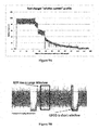
- Figure 9A illustrates a fast charger "relative current" profile while Figure 9B illustrates an example charging window.
- Wireless power charging is noisy due to AP loading, device use during phone charging, and thermal throttling adds to the noise profile.
- the FOD using coil current sensing described herein uses a long window for low noise. In particular, a number of measurements are averaged together, which improves SNR greatly with no impact on power transfer.
- the Q-factor of the circuit may be measured and stored, e.g., in time domain as a decay rate of transmitter coil self-resonance, or in frequency domain as a ratio of the peak frequency to the system bandwidth.
- the measured Q-factor value may be compared with a reference Q-factor value received from the receiving device to determine whether a foreign object is detected.
- a short measurement window is usually used in QFOD, which results in high noise.
- the short measurement window yields only a few data points (e.g., 10-12 data points), which is highly susceptible to noise. Low SNR adds error to results.
- running QFOD may often disrupt power transfer, e.g., for Q-factor measurement. Consequently, the FOD using coil current sensing described herein may yield greater performance than using QFOD.
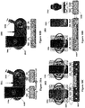
- FIGs 10B-10D provide different examples of multi-coil transmitters for multi-device charging.
- Each wireless power charger 1005 can be similar to the wireless transmitter 102 in Figure 1 .
- the wireless charger 1005 is configured to provide power transfer to two devices 104a and 104b.
- a single Tx controller chip may be configured to drive multiple coils to transfer power to multiple devices 104a and 104b.
- the wireless charger 1005 may be equipped with multiple coils 1007 placed at different positions and/or orientations for each charging area.
- the wireless charger 1005 also includes X-Y position sensors to identify a position of the device 104a or 104b placed at the charging area to as to transfer wireless power.
- wireless charger 1005 provides spatial freedom to the devices 104a or 104b and is able to charge a variety of different types of devices.
- the wireless charger 1005 may be equipped with a hybrid of different charging plates, e.g., a charging plate with X-Y position sensors, or a charging plate designed for a specific shape of a device such as a pad or a watch, etc.
- the different charging plates can be driven by a single Tx controller chip.
- Diagram 1004 further illustrates an embodiment in which another wireless charger 1006 may be connected to wireless charger 1005, via a wired connection or wirelessly, such that an authentication link may be established between the charger 1005 and 1006 through which the charging device(s) 104a-b may authenticate the charging device 104c.
- the wireless charger 1005 may include the coil sensing circuits shown in Figures 3-5 , and adopts the coil sensing method discussed in Figure 7 . In this way, the wireless charger 1005 computes a transmitter power loss based on coil current with enhanced precision for FOD during the wireless power transfer.
- the wireless charger 1005, . for example, as shown at diagrams 1003, 1004, the larger charging plate of the wireless charger 1005 contains multiple coils (e.g., 3, etc.), which allows greater X-Y position freedom such that the charging device 104a may be placed at different positions (e.g., 3 different positions according to the 3 coils in charger 1005) for charging.
Landscapes
- Engineering & Computer Science (AREA)
- Power Engineering (AREA)
- Computer Networks & Wireless Communication (AREA)
- Physics & Mathematics (AREA)
- Remote Sensing (AREA)
- Life Sciences & Earth Sciences (AREA)
- Geology (AREA)
- General Life Sciences & Earth Sciences (AREA)
- General Physics & Mathematics (AREA)
- Geophysics (AREA)
- Environmental & Geological Engineering (AREA)
- Electromagnetism (AREA)
- Charge And Discharge Circuits For Batteries Or The Like (AREA)
Priority Applications (1)
| Application Number | Priority Date | Filing Date | Title |
|---|---|---|---|
| EP23156327.1A EP4213342A1 (fr) | 2018-11-28 | 2019-11-27 | Détection améliorée d'objets étrangers avec détection de courant de bobine dans des systèmes de transfert d'énergie sans fil |
Applications Claiming Priority (4)
| Application Number | Priority Date | Filing Date | Title |
|---|---|---|---|
| US201862772592P | 2018-11-28 | 2018-11-28 | |
| US201962821899P | 2019-03-21 | 2019-03-21 | |
| US16/403,419 US11527920B2 (en) | 2018-11-28 | 2019-05-03 | Enhanced foreign object detection with coil current sensing in wireless power transfer systems |
| US16/586,212 US11418067B2 (en) | 2018-11-28 | 2019-09-27 | Enhanced foreign object detection with coil current sensing in wireless power transfer systems |
Related Child Applications (2)
| Application Number | Title | Priority Date | Filing Date |
|---|---|---|---|
| EP23156327.1A Division-Into EP4213342A1 (fr) | 2018-11-28 | 2019-11-27 | Détection améliorée d'objets étrangers avec détection de courant de bobine dans des systèmes de transfert d'énergie sans fil |
| EP23156327.1A Division EP4213342A1 (fr) | 2018-11-28 | 2019-11-27 | Détection améliorée d'objets étrangers avec détection de courant de bobine dans des systèmes de transfert d'énergie sans fil |
Publications (2)
| Publication Number | Publication Date |
|---|---|
| EP3661014A1 true EP3661014A1 (fr) | 2020-06-03 |
| EP3661014B1 EP3661014B1 (fr) | 2023-03-29 |
Family
ID=68731688
Family Applications (1)
| Application Number | Title | Priority Date | Filing Date |
|---|---|---|---|
| EP19211875.0A Active EP3661014B1 (fr) | 2018-11-28 | 2019-11-27 | Amélioration de la détection des corps étrangers grâce à la détection du courant de bobine dans les systèmes de transfert d'énergie sans fil |
Country Status (2)
| Country | Link |
|---|---|
| US (1) | US11418067B2 (fr) |
| EP (1) | EP3661014B1 (fr) |
Families Citing this family (6)
| Publication number | Priority date | Publication date | Assignee | Title |
|---|---|---|---|---|
| CN111313569A (zh) * | 2018-12-11 | 2020-06-19 | 恩智浦美国有限公司 | 无线充电系统中的异物检测电路的q因子确定 |
| US11881720B2 (en) | 2019-09-12 | 2024-01-23 | Spark Connected LLC | Electronic device, wireless charger and wireless charging system |
| US20230105687A1 (en) * | 2020-03-20 | 2023-04-06 | InductEV, Inc. | Current sensing in a wireless power transfer system |
| US12003117B2 (en) * | 2020-06-15 | 2024-06-04 | The Regents Of The University Of Michigan | Foreign object detection in wireless power transfer |
| DE102021203742A1 (de) * | 2021-04-15 | 2022-10-20 | Osram Gmbh | Strommessvorrichtung für getaktete leistungswandler und regelungsschaltung zur anwendung der strommessvorrichtung |
| US11916406B1 (en) * | 2021-09-16 | 2024-02-27 | Apple Inc. | Techniques for wireless power systems power delivery |
Citations (4)
| Publication number | Priority date | Publication date | Assignee | Title |
|---|---|---|---|---|
| US20160218520A1 (en) * | 2015-01-22 | 2016-07-28 | Integrated Device Technology, Inc. | Apparatuses and related methods for detecting magnetic flux field characteristics with a wireless power receiver |
| US20160309418A1 (en) * | 2015-04-16 | 2016-10-20 | Nxp B.V. | Method and system for performing foreign object detection in an inductive wireless power transfer system |
| US20170163100A1 (en) * | 2014-06-20 | 2017-06-08 | Powerbyproxi Limited | Foreign object detection in inductive power transfer field |
| US20170366048A1 (en) * | 2015-03-04 | 2017-12-21 | Rohm Co., Ltd. | Wireless power transmitter |
Family Cites Families (1)
| Publication number | Priority date | Publication date | Assignee | Title |
|---|---|---|---|---|
| TWI489729B (zh) * | 2013-11-18 | 2015-06-21 | Richtek Technology Corp | 適用於無線電力系統的電力計算的方法 |
-
2019
- 2019-09-27 US US16/586,212 patent/US11418067B2/en active Active
- 2019-11-27 EP EP19211875.0A patent/EP3661014B1/fr active Active
Patent Citations (4)
| Publication number | Priority date | Publication date | Assignee | Title |
|---|---|---|---|---|
| US20170163100A1 (en) * | 2014-06-20 | 2017-06-08 | Powerbyproxi Limited | Foreign object detection in inductive power transfer field |
| US20160218520A1 (en) * | 2015-01-22 | 2016-07-28 | Integrated Device Technology, Inc. | Apparatuses and related methods for detecting magnetic flux field characteristics with a wireless power receiver |
| US20170366048A1 (en) * | 2015-03-04 | 2017-12-21 | Rohm Co., Ltd. | Wireless power transmitter |
| US20160309418A1 (en) * | 2015-04-16 | 2016-10-20 | Nxp B.V. | Method and system for performing foreign object detection in an inductive wireless power transfer system |
Also Published As
| Publication number | Publication date |
|---|---|
| US11418067B2 (en) | 2022-08-16 |
| US20200169124A1 (en) | 2020-05-28 |
| EP3661014B1 (fr) | 2023-03-29 |
Similar Documents
| Publication | Publication Date | Title |
|---|---|---|
| EP4213342A1 (fr) | Détection améliorée d'objets étrangers avec détection de courant de bobine dans des systèmes de transfert d'énergie sans fil | |
| EP3661014B1 (fr) | Amélioration de la détection des corps étrangers grâce à la détection du courant de bobine dans les systèmes de transfert d'énergie sans fil | |
| US11527920B2 (en) | Enhanced foreign object detection with coil current sensing in wireless power transfer systems | |
| US20210083522A1 (en) | Input parasitic metal detection | |
| US10879743B2 (en) | Foreign object detection in inductive power transfer field | |
| EP2946455B1 (fr) | Récepteur de puissance, système de transmission de puissance sans contact et procédé de commande d'une tension de puissance reçue | |
| JP4741583B2 (ja) | 誘導電力転送システムの制御 | |
| US9866051B2 (en) | Adaptive charger to maximize charge rate | |
| US11190058B2 (en) | Non-contact power supply device and method for abnormal stop | |
| US11095160B2 (en) | Non-contact power supply device | |
| US20110194316A1 (en) | Switching power supply device | |
| US20130334893A1 (en) | Power transmission system and power transmitting apparatus | |
| JP6699883B2 (ja) | 非接触電力伝送システム、および、送電装置 | |
| KR20150115339A (ko) | 무선전력전송 시스템 | |
| JP2015186392A (ja) | 送電機器及び非接触電力伝送装置 | |
| WO2012073472A1 (fr) | Système de transmission de puissance électrique | |
| US11245291B2 (en) | Non-contact power supply device capable of performing constant voltage output operation | |
| US20210376642A1 (en) | Electronic device to wirelessly receive power and operating method thereof | |
| JP2021002991A (ja) | 絶縁型dcdcコンバータ | |
| JP2017041921A (ja) | 送電機器 | |
| CN112673545A (zh) | 非接触电力传输系统 | |
| JP7100734B1 (ja) | ワイヤレス受電装置 | |
| KR101360744B1 (ko) | 무선전력 송신장치, 무선전력 수신장치, 무선전력 전송 시스템 및 무선전력 전송 방법 | |
| WO2020144963A1 (fr) | Système de transmission d'énergie sans contact | |
| JP2015062339A (ja) | 制御装置、無線電力伝送装置および電力伝送効率推定方法 |
Legal Events
| Date | Code | Title | Description |
|---|---|---|---|
| PUAI | Public reference made under article 153(3) epc to a published international application that has entered the european phase |
Free format text: ORIGINAL CODE: 0009012 |
|
| STAA | Information on the status of an ep patent application or granted ep patent |
Free format text: STATUS: THE APPLICATION HAS BEEN PUBLISHED |
|
| AK | Designated contracting states |
Kind code of ref document: A1 Designated state(s): AL AT BE BG CH CY CZ DE DK EE ES FI FR GB GR HR HU IE IS IT LI LT LU LV MC MK MT NL NO PL PT RO RS SE SI SK SM TR |
|
| AX | Request for extension of the european patent |
Extension state: BA ME |
|
| STAA | Information on the status of an ep patent application or granted ep patent |
Free format text: STATUS: REQUEST FOR EXAMINATION WAS MADE |
|
| 17P | Request for examination filed |
Effective date: 20201203 |
|
| RBV | Designated contracting states (corrected) |
Designated state(s): AL AT BE BG CH CY CZ DE DK EE ES FI FR GB GR HR HU IE IS IT LI LT LU LV MC MK MT NL NO PL PT RO RS SE SI SK SM TR |
|
| STAA | Information on the status of an ep patent application or granted ep patent |
Free format text: STATUS: EXAMINATION IS IN PROGRESS |
|
| 17Q | First examination report despatched |
Effective date: 20210628 |
|
| GRAP | Despatch of communication of intention to grant a patent |
Free format text: ORIGINAL CODE: EPIDOSNIGR1 |
|
| STAA | Information on the status of an ep patent application or granted ep patent |
Free format text: STATUS: GRANT OF PATENT IS INTENDED |
|
| INTG | Intention to grant announced |
Effective date: 20220617 |
|
| GRAJ | Information related to disapproval of communication of intention to grant by the applicant or resumption of examination proceedings by the epo deleted |
Free format text: ORIGINAL CODE: EPIDOSDIGR1 |
|
| STAA | Information on the status of an ep patent application or granted ep patent |
Free format text: STATUS: EXAMINATION IS IN PROGRESS |
|
| INTC | Intention to grant announced (deleted) | ||
| GRAP | Despatch of communication of intention to grant a patent |
Free format text: ORIGINAL CODE: EPIDOSNIGR1 |
|
| STAA | Information on the status of an ep patent application or granted ep patent |
Free format text: STATUS: GRANT OF PATENT IS INTENDED |
|
| INTG | Intention to grant announced |
Effective date: 20221005 |
|
| GRAS | Grant fee paid |
Free format text: ORIGINAL CODE: EPIDOSNIGR3 |
|
| GRAA | (expected) grant |
Free format text: ORIGINAL CODE: 0009210 |
|
| STAA | Information on the status of an ep patent application or granted ep patent |
Free format text: STATUS: THE PATENT HAS BEEN GRANTED |
|
| AK | Designated contracting states |
Kind code of ref document: B1 Designated state(s): AL AT BE BG CH CY CZ DE DK EE ES FI FR GB GR HR HU IE IS IT LI LT LU LV MC MK MT NL NO PL PT RO RS SE SI SK SM TR |
|
| REG | Reference to a national code |
Ref country code: CH Ref legal event code: EP |
|
| REG | Reference to a national code |
Ref country code: DE Ref legal event code: R096 Ref document number: 602019026850 Country of ref document: DE |
|
| REG | Reference to a national code |
Ref country code: AT Ref legal event code: REF Ref document number: 1557347 Country of ref document: AT Kind code of ref document: T Effective date: 20230415 |
|
| REG | Reference to a national code |
Ref country code: IE Ref legal event code: FG4D |
|
| REG | Reference to a national code |
Ref country code: LT Ref legal event code: MG9D |
|
| PG25 | Lapsed in a contracting state [announced via postgrant information from national office to epo] |
Ref country code: RS Free format text: LAPSE BECAUSE OF FAILURE TO SUBMIT A TRANSLATION OF THE DESCRIPTION OR TO PAY THE FEE WITHIN THE PRESCRIBED TIME-LIMIT Effective date: 20230329 Ref country code: NO Free format text: LAPSE BECAUSE OF FAILURE TO SUBMIT A TRANSLATION OF THE DESCRIPTION OR TO PAY THE FEE WITHIN THE PRESCRIBED TIME-LIMIT Effective date: 20230629 Ref country code: LV Free format text: LAPSE BECAUSE OF FAILURE TO SUBMIT A TRANSLATION OF THE DESCRIPTION OR TO PAY THE FEE WITHIN THE PRESCRIBED TIME-LIMIT Effective date: 20230329 Ref country code: LT Free format text: LAPSE BECAUSE OF FAILURE TO SUBMIT A TRANSLATION OF THE DESCRIPTION OR TO PAY THE FEE WITHIN THE PRESCRIBED TIME-LIMIT Effective date: 20230329 Ref country code: HR Free format text: LAPSE BECAUSE OF FAILURE TO SUBMIT A TRANSLATION OF THE DESCRIPTION OR TO PAY THE FEE WITHIN THE PRESCRIBED TIME-LIMIT Effective date: 20230329 |
|
| REG | Reference to a national code |
Ref country code: NL Ref legal event code: MP Effective date: 20230329 |
|
| REG | Reference to a national code |
Ref country code: AT Ref legal event code: MK05 Ref document number: 1557347 Country of ref document: AT Kind code of ref document: T Effective date: 20230329 |
|
| PG25 | Lapsed in a contracting state [announced via postgrant information from national office to epo] |
Ref country code: SE Free format text: LAPSE BECAUSE OF FAILURE TO SUBMIT A TRANSLATION OF THE DESCRIPTION OR TO PAY THE FEE WITHIN THE PRESCRIBED TIME-LIMIT Effective date: 20230329 Ref country code: NL Free format text: LAPSE BECAUSE OF FAILURE TO SUBMIT A TRANSLATION OF THE DESCRIPTION OR TO PAY THE FEE WITHIN THE PRESCRIBED TIME-LIMIT Effective date: 20230329 Ref country code: GR Free format text: LAPSE BECAUSE OF FAILURE TO SUBMIT A TRANSLATION OF THE DESCRIPTION OR TO PAY THE FEE WITHIN THE PRESCRIBED TIME-LIMIT Effective date: 20230630 Ref country code: FI Free format text: LAPSE BECAUSE OF FAILURE TO SUBMIT A TRANSLATION OF THE DESCRIPTION OR TO PAY THE FEE WITHIN THE PRESCRIBED TIME-LIMIT Effective date: 20230329 |
|
| PG25 | Lapsed in a contracting state [announced via postgrant information from national office to epo] |
Ref country code: SM Free format text: LAPSE BECAUSE OF FAILURE TO SUBMIT A TRANSLATION OF THE DESCRIPTION OR TO PAY THE FEE WITHIN THE PRESCRIBED TIME-LIMIT Effective date: 20230329 Ref country code: RO Free format text: LAPSE BECAUSE OF FAILURE TO SUBMIT A TRANSLATION OF THE DESCRIPTION OR TO PAY THE FEE WITHIN THE PRESCRIBED TIME-LIMIT Effective date: 20230329 Ref country code: PT Free format text: LAPSE BECAUSE OF FAILURE TO SUBMIT A TRANSLATION OF THE DESCRIPTION OR TO PAY THE FEE WITHIN THE PRESCRIBED TIME-LIMIT Effective date: 20230731 Ref country code: ES Free format text: LAPSE BECAUSE OF FAILURE TO SUBMIT A TRANSLATION OF THE DESCRIPTION OR TO PAY THE FEE WITHIN THE PRESCRIBED TIME-LIMIT Effective date: 20230329 Ref country code: EE Free format text: LAPSE BECAUSE OF FAILURE TO SUBMIT A TRANSLATION OF THE DESCRIPTION OR TO PAY THE FEE WITHIN THE PRESCRIBED TIME-LIMIT Effective date: 20230329 Ref country code: AT Free format text: LAPSE BECAUSE OF FAILURE TO SUBMIT A TRANSLATION OF THE DESCRIPTION OR TO PAY THE FEE WITHIN THE PRESCRIBED TIME-LIMIT Effective date: 20230329 |
|
| PG25 | Lapsed in a contracting state [announced via postgrant information from national office to epo] |
Ref country code: SK Free format text: LAPSE BECAUSE OF FAILURE TO SUBMIT A TRANSLATION OF THE DESCRIPTION OR TO PAY THE FEE WITHIN THE PRESCRIBED TIME-LIMIT Effective date: 20230329 Ref country code: PL Free format text: LAPSE BECAUSE OF FAILURE TO SUBMIT A TRANSLATION OF THE DESCRIPTION OR TO PAY THE FEE WITHIN THE PRESCRIBED TIME-LIMIT Effective date: 20230329 Ref country code: IS Free format text: LAPSE BECAUSE OF FAILURE TO SUBMIT A TRANSLATION OF THE DESCRIPTION OR TO PAY THE FEE WITHIN THE PRESCRIBED TIME-LIMIT Effective date: 20230729 |
|
| REG | Reference to a national code |
Ref country code: DE Ref legal event code: R097 Ref document number: 602019026850 Country of ref document: DE |
|
| PG25 | Lapsed in a contracting state [announced via postgrant information from national office to epo] |
Ref country code: DK Free format text: LAPSE BECAUSE OF FAILURE TO SUBMIT A TRANSLATION OF THE DESCRIPTION OR TO PAY THE FEE WITHIN THE PRESCRIBED TIME-LIMIT Effective date: 20230329 Ref country code: CZ Free format text: LAPSE BECAUSE OF FAILURE TO SUBMIT A TRANSLATION OF THE DESCRIPTION OR TO PAY THE FEE WITHIN THE PRESCRIBED TIME-LIMIT Effective date: 20230329 |
|
| PLBE | No opposition filed within time limit |
Free format text: ORIGINAL CODE: 0009261 |
|
| STAA | Information on the status of an ep patent application or granted ep patent |
Free format text: STATUS: NO OPPOSITION FILED WITHIN TIME LIMIT |
|
| 26N | No opposition filed |
Effective date: 20240103 |
|
| PG25 | Lapsed in a contracting state [announced via postgrant information from national office to epo] |
Ref country code: SI Free format text: LAPSE BECAUSE OF FAILURE TO SUBMIT A TRANSLATION OF THE DESCRIPTION OR TO PAY THE FEE WITHIN THE PRESCRIBED TIME-LIMIT Effective date: 20230329 |
|
| PG25 | Lapsed in a contracting state [announced via postgrant information from national office to epo] |
Ref country code: SI Free format text: LAPSE BECAUSE OF FAILURE TO SUBMIT A TRANSLATION OF THE DESCRIPTION OR TO PAY THE FEE WITHIN THE PRESCRIBED TIME-LIMIT Effective date: 20230329 Ref country code: IT Free format text: LAPSE BECAUSE OF FAILURE TO SUBMIT A TRANSLATION OF THE DESCRIPTION OR TO PAY THE FEE WITHIN THE PRESCRIBED TIME-LIMIT Effective date: 20230329 |
|
| REG | Reference to a national code |
Ref country code: CH Ref legal event code: PL |
|
| PG25 | Lapsed in a contracting state [announced via postgrant information from national office to epo] |
Ref country code: MC Free format text: LAPSE BECAUSE OF FAILURE TO SUBMIT A TRANSLATION OF THE DESCRIPTION OR TO PAY THE FEE WITHIN THE PRESCRIBED TIME-LIMIT Effective date: 20230329 |
|
| PGFP | Annual fee paid to national office [announced via postgrant information from national office to epo] |
Ref country code: DE Payment date: 20240503 Year of fee payment: 5 |
|
| PG25 | Lapsed in a contracting state [announced via postgrant information from national office to epo] |
Ref country code: LU Free format text: LAPSE BECAUSE OF NON-PAYMENT OF DUE FEES Effective date: 20231127 |
|
| PG25 | Lapsed in a contracting state [announced via postgrant information from national office to epo] |
Ref country code: CH Free format text: LAPSE BECAUSE OF NON-PAYMENT OF DUE FEES Effective date: 20231130 |
|
| GBPC | Gb: european patent ceased through non-payment of renewal fee |
Effective date: 20231127 |
|
| PG25 | Lapsed in a contracting state [announced via postgrant information from national office to epo] |
Ref country code: MC Free format text: LAPSE BECAUSE OF FAILURE TO SUBMIT A TRANSLATION OF THE DESCRIPTION OR TO PAY THE FEE WITHIN THE PRESCRIBED TIME-LIMIT Effective date: 20230329 Ref country code: LU Free format text: LAPSE BECAUSE OF NON-PAYMENT OF DUE FEES Effective date: 20231127 Ref country code: CH Free format text: LAPSE BECAUSE OF NON-PAYMENT OF DUE FEES Effective date: 20231130 |
|
| REG | Reference to a national code |
Ref country code: BE Ref legal event code: MM Effective date: 20231130 |
|
| REG | Reference to a national code |
Ref country code: IE Ref legal event code: MM4A |