EP3650575A1 - Vapor deposition mask, vapor deposition mask device, vapor deposition mask manufacturing method and vapor deposition mask device manufacturing method - Google Patents
Vapor deposition mask, vapor deposition mask device, vapor deposition mask manufacturing method and vapor deposition mask device manufacturing method Download PDFInfo
- Publication number
- EP3650575A1 EP3650575A1 EP18827999.6A EP18827999A EP3650575A1 EP 3650575 A1 EP3650575 A1 EP 3650575A1 EP 18827999 A EP18827999 A EP 18827999A EP 3650575 A1 EP3650575 A1 EP 3650575A1
- Authority
- EP
- European Patent Office
- Prior art keywords
- mask
- deposition mask
- deposition
- metal layer
- substrate
- Prior art date
- Legal status (The legal status is an assumption and is not a legal conclusion. Google has not performed a legal analysis and makes no representation as to the accuracy of the status listed.)
- Pending
Links
Images



Classifications
-
- C—CHEMISTRY; METALLURGY
- C23—COATING METALLIC MATERIAL; COATING MATERIAL WITH METALLIC MATERIAL; CHEMICAL SURFACE TREATMENT; DIFFUSION TREATMENT OF METALLIC MATERIAL; COATING BY VACUUM EVAPORATION, BY SPUTTERING, BY ION IMPLANTATION OR BY CHEMICAL VAPOUR DEPOSITION, IN GENERAL; INHIBITING CORROSION OF METALLIC MATERIAL OR INCRUSTATION IN GENERAL
- C23C—COATING METALLIC MATERIAL; COATING MATERIAL WITH METALLIC MATERIAL; SURFACE TREATMENT OF METALLIC MATERIAL BY DIFFUSION INTO THE SURFACE, BY CHEMICAL CONVERSION OR SUBSTITUTION; COATING BY VACUUM EVAPORATION, BY SPUTTERING, BY ION IMPLANTATION OR BY CHEMICAL VAPOUR DEPOSITION, IN GENERAL
- C23C14/00—Coating by vacuum evaporation, by sputtering or by ion implantation of the coating forming material
- C23C14/04—Coating on selected surface areas, e.g. using masks
- C23C14/042—Coating on selected surface areas, e.g. using masks using masks
-
- C—CHEMISTRY; METALLURGY
- C23—COATING METALLIC MATERIAL; COATING MATERIAL WITH METALLIC MATERIAL; CHEMICAL SURFACE TREATMENT; DIFFUSION TREATMENT OF METALLIC MATERIAL; COATING BY VACUUM EVAPORATION, BY SPUTTERING, BY ION IMPLANTATION OR BY CHEMICAL VAPOUR DEPOSITION, IN GENERAL; INHIBITING CORROSION OF METALLIC MATERIAL OR INCRUSTATION IN GENERAL
- C23C—COATING METALLIC MATERIAL; COATING MATERIAL WITH METALLIC MATERIAL; SURFACE TREATMENT OF METALLIC MATERIAL BY DIFFUSION INTO THE SURFACE, BY CHEMICAL CONVERSION OR SUBSTITUTION; COATING BY VACUUM EVAPORATION, BY SPUTTERING, BY ION IMPLANTATION OR BY CHEMICAL VAPOUR DEPOSITION, IN GENERAL
- C23C14/00—Coating by vacuum evaporation, by sputtering or by ion implantation of the coating forming material
- C23C14/04—Coating on selected surface areas, e.g. using masks
-
- C—CHEMISTRY; METALLURGY
- C23—COATING METALLIC MATERIAL; COATING MATERIAL WITH METALLIC MATERIAL; CHEMICAL SURFACE TREATMENT; DIFFUSION TREATMENT OF METALLIC MATERIAL; COATING BY VACUUM EVAPORATION, BY SPUTTERING, BY ION IMPLANTATION OR BY CHEMICAL VAPOUR DEPOSITION, IN GENERAL; INHIBITING CORROSION OF METALLIC MATERIAL OR INCRUSTATION IN GENERAL
- C23C—COATING METALLIC MATERIAL; COATING MATERIAL WITH METALLIC MATERIAL; SURFACE TREATMENT OF METALLIC MATERIAL BY DIFFUSION INTO THE SURFACE, BY CHEMICAL CONVERSION OR SUBSTITUTION; COATING BY VACUUM EVAPORATION, BY SPUTTERING, BY ION IMPLANTATION OR BY CHEMICAL VAPOUR DEPOSITION, IN GENERAL
- C23C14/00—Coating by vacuum evaporation, by sputtering or by ion implantation of the coating forming material
- C23C14/06—Coating by vacuum evaporation, by sputtering or by ion implantation of the coating forming material characterised by the coating material
- C23C14/12—Organic material
-
- C—CHEMISTRY; METALLURGY
- C23—COATING METALLIC MATERIAL; COATING MATERIAL WITH METALLIC MATERIAL; CHEMICAL SURFACE TREATMENT; DIFFUSION TREATMENT OF METALLIC MATERIAL; COATING BY VACUUM EVAPORATION, BY SPUTTERING, BY ION IMPLANTATION OR BY CHEMICAL VAPOUR DEPOSITION, IN GENERAL; INHIBITING CORROSION OF METALLIC MATERIAL OR INCRUSTATION IN GENERAL
- C23C—COATING METALLIC MATERIAL; COATING MATERIAL WITH METALLIC MATERIAL; SURFACE TREATMENT OF METALLIC MATERIAL BY DIFFUSION INTO THE SURFACE, BY CHEMICAL CONVERSION OR SUBSTITUTION; COATING BY VACUUM EVAPORATION, BY SPUTTERING, BY ION IMPLANTATION OR BY CHEMICAL VAPOUR DEPOSITION, IN GENERAL
- C23C14/00—Coating by vacuum evaporation, by sputtering or by ion implantation of the coating forming material
- C23C14/22—Coating by vacuum evaporation, by sputtering or by ion implantation of the coating forming material characterised by the process of coating
- C23C14/24—Vacuum evaporation
-
- C—CHEMISTRY; METALLURGY
- C23—COATING METALLIC MATERIAL; COATING MATERIAL WITH METALLIC MATERIAL; CHEMICAL SURFACE TREATMENT; DIFFUSION TREATMENT OF METALLIC MATERIAL; COATING BY VACUUM EVAPORATION, BY SPUTTERING, BY ION IMPLANTATION OR BY CHEMICAL VAPOUR DEPOSITION, IN GENERAL; INHIBITING CORROSION OF METALLIC MATERIAL OR INCRUSTATION IN GENERAL
- C23F—NON-MECHANICAL REMOVAL OF METALLIC MATERIAL FROM SURFACE; INHIBITING CORROSION OF METALLIC MATERIAL OR INCRUSTATION IN GENERAL; MULTI-STEP PROCESSES FOR SURFACE TREATMENT OF METALLIC MATERIAL INVOLVING AT LEAST ONE PROCESS PROVIDED FOR IN CLASS C23 AND AT LEAST ONE PROCESS COVERED BY SUBCLASS C21D OR C22F OR CLASS C25
- C23F1/00—Etching metallic material by chemical means
- C23F1/02—Local etching
-
- H—ELECTRICITY
- H05—ELECTRIC TECHNIQUES NOT OTHERWISE PROVIDED FOR
- H05B—ELECTRIC HEATING; ELECTRIC LIGHT SOURCES NOT OTHERWISE PROVIDED FOR; CIRCUIT ARRANGEMENTS FOR ELECTRIC LIGHT SOURCES, IN GENERAL
- H05B33/00—Electroluminescent light sources
- H05B33/10—Apparatus or processes specially adapted to the manufacture of electroluminescent light sources
-
- H—ELECTRICITY
- H10—SEMICONDUCTOR DEVICES; ELECTRIC SOLID-STATE DEVICES NOT OTHERWISE PROVIDED FOR
- H10K—ORGANIC ELECTRIC SOLID-STATE DEVICES
- H10K71/00—Manufacture or treatment specially adapted for the organic devices covered by this subclass
- H10K71/10—Deposition of organic active material
- H10K71/16—Deposition of organic active material using physical vapour deposition [PVD], e.g. vacuum deposition or sputtering
- H10K71/164—Deposition of organic active material using physical vapour deposition [PVD], e.g. vacuum deposition or sputtering using vacuum deposition
-
- H—ELECTRICITY
- H10—SEMICONDUCTOR DEVICES; ELECTRIC SOLID-STATE DEVICES NOT OTHERWISE PROVIDED FOR
- H10K—ORGANIC ELECTRIC SOLID-STATE DEVICES
- H10K71/00—Manufacture or treatment specially adapted for the organic devices covered by this subclass
- H10K71/10—Deposition of organic active material
- H10K71/16—Deposition of organic active material using physical vapour deposition [PVD], e.g. vacuum deposition or sputtering
- H10K71/166—Deposition of organic active material using physical vapour deposition [PVD], e.g. vacuum deposition or sputtering using selective deposition, e.g. using a mask
-
- H—ELECTRICITY
- H10—SEMICONDUCTOR DEVICES; ELECTRIC SOLID-STATE DEVICES NOT OTHERWISE PROVIDED FOR
- H10P—GENERIC PROCESSES OR APPARATUS FOR THE MANUFACTURE OR TREATMENT OF DEVICES COVERED BY CLASS H10
- H10P76/00—Manufacture or treatment of masks on semiconductor bodies, e.g. by lithography or photolithography
- H10P76/40—Manufacture or treatment of masks on semiconductor bodies, e.g. by lithography or photolithography of masks comprising inorganic materials
- H10P76/405—Manufacture or treatment of masks on semiconductor bodies, e.g. by lithography or photolithography of masks comprising inorganic materials characterised by their composition, e.g. multilayer masks
-
- H—ELECTRICITY
- H10—SEMICONDUCTOR DEVICES; ELECTRIC SOLID-STATE DEVICES NOT OTHERWISE PROVIDED FOR
- H10P—GENERIC PROCESSES OR APPARATUS FOR THE MANUFACTURE OR TREATMENT OF DEVICES COVERED BY CLASS H10
- H10P76/00—Manufacture or treatment of masks on semiconductor bodies, e.g. by lithography or photolithography
- H10P76/40—Manufacture or treatment of masks on semiconductor bodies, e.g. by lithography or photolithography of masks comprising inorganic materials
- H10P76/408—Manufacture or treatment of masks on semiconductor bodies, e.g. by lithography or photolithography of masks comprising inorganic materials characterised by their sizes, orientations, dispositions, behaviours or shapes
- H10P76/4085—Manufacture or treatment of masks on semiconductor bodies, e.g. by lithography or photolithography of masks comprising inorganic materials characterised by their sizes, orientations, dispositions, behaviours or shapes characterised by the processes involved to create the masks
-
- H—ELECTRICITY
- H10—SEMICONDUCTOR DEVICES; ELECTRIC SOLID-STATE DEVICES NOT OTHERWISE PROVIDED FOR
- H10K—ORGANIC ELECTRIC SOLID-STATE DEVICES
- H10K50/00—Organic light-emitting devices
Definitions
- the present disclosure relates to a deposition mask that is used for depositing a deposition material onto a substrate to be deposited (a substrate onto which the deposition material is deposited), a deposition mask apparatus, a manufacturing method of a deposition mask, and a manufacturing method of a deposition mask apparatus.
- a display device used in a portable device such as a smart phone and a tablet PC is required to have high fineness, e.g., a pixel density of not less than 400 ppi.
- the portable device is applicable in the ultra full high-definitions reference.
- the pixel density of the display device needs to be not less than 800 ppi or more, for example.
- An organic EL display device draws attention because of its excellent responsibility, low power consumption and excellent contrast.
- a known method for forming pixels of an organic EL display device is a method which uses a deposition mask including through-holes that are arranged in a desired pattern, and forms pixels in the desired pattern.
- a substrate for an organic EL display device (substrate for organic EL) is firstly put into a deposition apparatus. Then, a deposition step in which a deposition mask is brought into contact with the substrate for organic EL so as to deposit an organic material onto the substrate for organic EL is carried out in the deposition apparatus.
- a deposition mask disclosed in JP2016-148112A can be given as an example of such a deposition mask.
- the deposition mask disclosed in JP2016-148112A is manufactured by a plating process.
- a conductive pattern is formed on an insulating substrate, and then a metal layer is formed on the conductive pattern by means of an electrolytic plating method. Thereafter, by removing the substrate and the conductive pattern, a deposition mask with the metal layer can be obtained.
- This technique is advantageous in that a thinned deposition mask can be obtained because the deposition mask is manufactured by a plating process.
- a deposition material which moves toward a substrate to be deposited such as an substrate for organic EL from a direction that is largely inclined with respect to a normal direction of a plate surface of the deposition mask can be allowed to suitably adhere to the substrate to be deposited exposed to through-holes of the deposition mask.
- a deposition mask is manufactured by using a plating process, and then the deposition mask is attached to a frame so as to manufacture a deposition mask apparatus.
- the frame of the deposition mask apparatus holds the deposition mask in a tensioned condition. Namely, tension is applied to the deposition mask which is fixed on the frame. Thus, the deposition mask is prevented from being bent.
- the present inventors have found that, since tension is applied to the thinned deposition mask, the deposition mask is disadvantageously wrinkled and/or deformed.
- a deposition mask and a deposition mask apparatus in the following method.
- a conductive pattern made of a conductive material, such as copper is provided on a substrate.
- a metal layer which will serve as a deposition mask is provided on the conductive pattern, so as to produce a laminated body including the substrate, the conductive pattern and the metal layer.
- the metal layer of the laminated body is joined to a frame by welding, for example.
- the conductive pattern is etched and removed, and the substrate is separated from the metal layer.
- a deposition mask formed of the metal layer, and a deposition mask apparatus having the deposition mask and the frame can be manufactured.
- the metal layer of the laminated body which will serve as the deposition mask, is joined to the frame while the metal layer is being held on the substrate, flatness of the deposition mask can be well ensured. Thus, it is considered that the deposition mask can be prevented from being wrinkled and/or deformed.
- the present inventors have found the following problem in this method.
- a residual stress internal stress
- a tensile force may be generated in a plane of the metal layer.
- a power of the tensile force varies depending on a thickness and/or a composition of the metal layer.
- the deposition mask formed of a plated layer inevitably has non-uniform thickness and/or composition in its plane. In this case, the tensile force in the plane of the deposition mask may become non-uniform.
- positions of respective through-holes are displaced from predetermined positions, because of the non-uniform tensile force in the plane.
- the present disclosure has been made in view of the above circumstances.
- the object of the present disclosure is to provide a deposition mask, a deposition mask apparatus, and a manufacturing method of a deposition mask and a deposition mask apparatus, capable of preventing positional displacement of through-holes.
- a deposition mask of the present disclosure comprises:
- a deposition mask of the present disclosure comprises the aforementioned deposition mask, and a frame attached to the deposition mask.
- a manufacturing method of a deposition mask of the present disclosure is a manufacturing method of a deposition mask including a first mask in which a plurality of openings arranged at least along a first direction are formed, and a second mask superposed on the first mask and having a plurality of through-holes formed therein, the through-hole having a planar dimension smaller than a planar dimension of the opening, the manufacturing method comprising:
- the plurality of joints may be arranged along an outer edge of the metal layer; and a notch may be formed at a position in the outer edge of the metal layer, the position corresponding to a space between the two joints that are adjacent to each other in the arrangement direction of the plurality of joints.
- a manufacturing method of a deposition mask apparatus of the present disclosure is a manufacturing method of a deposition mask apparatus including a deposition mask and a frame attached to the deposition mask, the manufacturing method comprising:
- the manufacturing method of a deposition mask apparatus of the present disclosure may further comprises, , before the attachment step, a stretching step in which the deposition mask is stretched in a planar direction thereof.
- the present disclosure can provide a deposition mask, a deposition mask apparatus, and a manufacturing method of a deposition mask and a deposition mask apparatus, capable of restraining positional displacement of through-holes.
- Figs. 1 to 31 are views for describing an embodiment of the present disclosure.
- a deposition mask apparatus used for patterning an organic material on a substrate in a desired pattern in order to manufacture an organic EL display device and a manufacturing method of the deposition mask apparatus are described by way of example.
- the present disclosure is not limited to this application, and can be applied to a deposition mask apparatus used for various purposes and a manufacturing method of the deposition mask apparatus.
- the terms “plate”, “sheet” and “film” are not differentiated from one another, based only on the difference in terms.
- the “plate” is a concept including a member that can be referred to as “sheet” or "film”.
- plate plane means a plane corresponding to a plane direction of a plate-like (sheet-like, film-like) member as a target, when the plate-like (sheet-like, film-like) member as a target is seen as a whole in general.
- a planar direction used for a plate-like (sheet-like, film-like) member means a direction parallel to a plate plane (sheet plane, film plane) of the member.
- a normal direction used to the plate-like (sheet-like, film-like) member means a normal direction with respect to a plate plane (sheet surface, film surface) of the member.
- the deposition apparatus 90 includes therein a deposition source (e.g., a crucible 94), a heater 96, and a deposition mask apparatus 10.
- the deposition apparatus 90 may further include exhaust means to create a vacuum atmosphere inside of the deposition apparatus 90.
- the crucible 94 accommodates a deposition material 98 such as an organic luminescent material.
- the heater 96 is configured to heat the crucible 94 so as to evaporate the deposition material 98 in the vacuum atmosphere.
- the deposition mask apparatus 10 is located opposite to the crucible 94.
- the deposition mask apparatus 10 includes a deposition mask 20 and a frame 12 for supporting the deposition mask 20.
- the frame 12 is configured to support the deposition mask 20 to pull it in a taut state in its planar direction in order to prevent the deposition mask 20 from warping.
- the deposition mask apparatus 10 is disposed in the deposition apparatus 90 such that the deposition mask 20 faces a substrate to be deposited (e.g., an substrate for organic EL) 92, which is an object onto which the deposition material 98 is to be deposited.
- a substrate to be deposited e.g., an substrate for organic EL
- the deposition mask apparatus 10 may include a magnet 93 disposed on a surface of the substrate for organic EL 92, which is opposite to the surface on the deposition mask 20 side.
- the deposition mask 20 can be attracted to the magnet 93 by magnetic force, so that the deposition mask 20 can be brought into tight contact with the substrate to be deposited 92.
- the deposition mask 20 includes a first mask 30 and a second mask 40 superposed on the first mask 30.
- the first mask 30 has a plate member 32 and a plurality of openings 35 formed in the plate member 32.
- the second mask 40 has a metal layer 42 and a plurality of through-holes 45 formed in the metal layer 42.
- a thickness of the first mask 30 is not less than 50 ⁇ m and not more than 3000 ⁇ m
- a thickness of the second mask 40 is not less than 2.5 ⁇ m and not more than 30 ⁇ m.
- the through-hole 45 has a planar dimension smaller than a planar dimension of the opening 35.
- the description that the through-hole 45 has a planar dimension smaller than a planar dimension of the opening 35 means that the dimension of the through-hole 45 is smaller than the dimension of the opening 35 in all the directions along a plate plane of the first mask 30 (a plate plane of the second mask 40).
- an outline delimiting the opening 35 surrounds outlines delimiting the through-holes 45 positioned in the opening 35.
- a maximum dimension of the through-hole 45 in the planar direction is not less than 5 ⁇ m and not more than 100 ⁇ m, for example.
- the through-hole 45 of the second mask 45 is also formed at a position that is not overlapped with the opening 35 of the first mask 30.
- the through-hole 45 may have a slit-like shape having a longitudinal direction and a width direction orthogonal to the longitudinal direction.
- a maximum width of the through-hole 45 along the width direction may be not less than 5 ⁇ m and not more than 100 ⁇ m, for example.
- the deposition mask 20 has a first surface 20a and a second surface 20b that defines a surface opposite to the first surface 20a.
- the deposition mask 20 is disposed between the substrate to be deposited 92 and the crucible 94.
- the deposition mask 20 is supported in the deposition apparatus 90 such that its second surface 20b faces a lower surface of the substrate to be deposited 92, in other words, such that its first surface 20a faces the crucible 94, and is used for depositing the deposition material 98 onto the substrate to be deposited 92.
- the deposition material 98 can be film-deposited onto the surface of the substrate to be deposited 92 in a desired pattern corresponding to the positions of the openings 35 of the first make 30 and the through-holes 45 of the second mask 40.
- Fig. 2 is a cross-sectional view showing an organic EL display device 100 manufactured by using the deposition apparatus 90 of Fig. 1 .
- the organic EL display device 100 includes the substrate to be deposited (substrate for organic EL) 92 and patterned pixels containing the deposition materials 98.
- deposition apparatuses 90 equipped with deposition masks 20 corresponding to the respective colors are prepared, and the substrate to be deposited 92 is introduced into each deposition apparatus 90. Accordingly, for example, an organic luminescent material for red color, an organic luminescent material for green color, and an organic luminescent material for blue color can be sequentially deposited on the substrate to be deposited 92.
- the deposition process is sometimes performed inside the deposition apparatus 90 in a high-temperature atmosphere.
- the deposition mask 20, the frame 12, and the substrate to be deposited 92 which are held inside the deposition apparatus 90, are also heated.
- the first mask 30 and the second mask 40 of deposition mask 20, the frame 12, and the substrate to be deposited 92 develop dimensional change behaviors based on their respective thermal expansion coefficients.
- the thermal expansion coefficients of the first mask 30, the second mask 40, the frame 12 and the substrate to be deposited 92 largely differ from one another, positioning displacement occurs because of the difference in dimensional change.
- dimensional precision and/or positional precision of the deposition material deposited onto the substrate to be deposited 92 decrease.
- the thermal expansion coefficients of the first mask 30, the second mask 40 and the frame 12 are preferably equivalent to the thermal expansion coefficient of the substrate to be deposited 92.
- an iron alloy containing nickel can be used as a main material of the first mask 30, the second mask 40 and the frame 12.
- an iron alloy containing nickel may be an invar material containing not less than 34% by mass and not more than 38% by mass of nickel, a super invar material containing cobalt in addition to not less than 30% by mass and not more than 34% by mass of nickel, and a low thermal expansion Fe-Ni based plated alloy not less than 38% by mass and not more than 54% by mass of nickel.
- a material other than the aforementioned iron alloy may be used as the material forming the first mask 30 and the second mask 40.
- an alloy other than the aforementioned iron alloy containing nickel such as an iron alloy containing chromium
- an iron alloy containing chromium for example, an iron alloy, which is called so-called stainless steel, can be used.
- alloys such as a nickel or nickel-cobalt alloy other than iron alloys may be used.
- Fig. 3 is a plan view schematically showing an example of the deposition mask apparatus 10 having the deposition mask 20, the deposition mask apparatus 10 being seen from the first surface 20 side.
- Fig. 4 is a cross-sectional view of the deposition mask apparatus 10, which shows the deposition mask 10 in a cross-section corresponding to a VI-VI line of Fig. 3 .
- the deposition mask 20 has an outline of, for example, a substantially quadrangular shape in a plan view, more precisely, a substantially rectangular shape in a plan view.
- the frame 12 is formed as a substantially rectangular frame.
- the deposition mask 20 is attached to the frame 12 such that each side of the deposition mask 20 corresponds to each side of the frame 12.
- the deposition mask 20 has the first mask 30 and the second mask 40 stacked on each other.
- the second mask 40 is disposed on the second surface 20b side with respect to the first mask 30.
- the surface of the first mask 30, which is opposite to the second mask 40, and the surface of the second mask 40, which is exposed from the opening 35 of the first mask 30, define the first surface 20a of the deposition mask 20.
- the surface of the second mask 40, which is opposed to the first mask 30, defines the second surface 20b of the deposition mask 20.
- the first mask 30 and the second mask 40 respectively have a substantially rectangular outline in a plan view.
- the first mask 30 has a planar dimension larger than a planar dimension of the second mask 40.
- the outline delimiting the first mask 30 surrounds the outline delimiting the second mask 40.
- the first mask 30 and the second mask 40 of the deposition mask 20 are fixed to each other.
- the deposition mask 20 has a plurality of first joints 16 that join the first mask 30 and the second mask 40 to each other.
- the first mask 30 and the frame 12 are fixed to each other.
- the deposition mask apparatus 10 has a plurality of second joints 18 that join the first mask 30 and the frame 12 to each other.
- the joints 16, 18 are respectively arranged along an outer edge 22 of the deposition mask 20. Particularly in the illustrated example, the outer edge 22 of the deposition mask 20 and an outer edge 43 of the second mask 40 extend parallel to each other, i.e., along the same direction.
- the deposition mask 20 has the substantially rectangular outline in a plan view.
- the joints 16, 18 are also arranged in a substantially rectangular pattern along the outer edge 22 of the deposition mask 20.
- the joints 16, 18 are respectively arranged linearly with a certain distance from the outer edge 22 of the deposition mask 20. Namely, the joints 16, 18 are arranged respectively along a direction parallel to the direction in which the outer edge 22 of the deposition mask 20 extends.
- the joints 16, 18 are respectively arranged equidistantly along the direction in which the outer edge 22 extends.
- the description that the joints 16, 18 are arranged along the outer edges 22, 43 means that the joints 16, 18 are arranged at least along a part of the entire circumferences of the outer edges 22, 43. In the illustrated example, the joints 16, 18 are arranged along the entire circumferences of the outer edges 22, 43. However, not limited thereto, the joints 16, 18 may be arranged along only two opposed sides of the entire circumferences of the outer edges 22, 43.
- the first mask 30 and the second mask 40 are fixed to each other by spot welding.
- the respective first joints 16 and the second joints 18 are formed as joints by spot welding.
- the first mask 30 and the second mask 40, and/or the first mask 30 and the frame 12 may be fixed to each other by another fixing means such as an adhesive. Namely, the respective first joints 16 and the second joints 18 may be formed as adhesive parts.
- Fig. 5 is a plan view showing the first mask 30 of the deposition mask apparatus 10 of Fig. 3 .
- the first mask 30 has the plurality of openings 35 which are arranged at predetermined pitches along a first direction D1 and a second direction D2.
- the first direction D1 and the second direction D2 are directions both parallel to a plane direction of the plate member 32 of the first mask 30.
- the second direction D2 is orthogonal to the first direction D1.
- the first mask 30 having a single layer is described by way of example.
- the first mask 30 may have a plurality of layers. Namely, the first mask 30 may be produced by laminating a plurality of layers along its plate plane direction.
- One opening 35 of the first mask 30 corresponds to one display area of the organic EL display device 100. Therefore, the illustrated deposition mask apparatus 10 enables a multifaceted deposition of the organic EL display device 100, correspondingly to the respective openings 35 of the first mask 30.
- the opening 35 has an outline of, for example, a substantially quadrangular shape in a plan view, more precisely, a substantially rectangular shape in a plan view.
- each opening 35 can have an outline of a different shape in accordance with the shape of the display area of the substrate to be deposited (substrate for organic EL) 92.
- each opening 35 may have a circular outline.
- Fig. 3 shows that the respective openings 35 have the same shape with each outer in a plan view.
- the respective openings 35 may have opening shapes different from one another.
- the first mask 30 may have a plurality of openings 35 having different shapes in a plan view.
- an alignment mark 37 is provided near a corner of each opening 35 of the first mask 30.
- one opening 35 is provided, correspondingly to four corners thereof, with four alignment marks 37.
- some (e.g., two) alignment marks 37 are shared by the openings 35 adjacent to each other.
- the alignment marks 37 are used when relative positions between the respective through-holes 45 of the second mask 40 exposed into the respective opening 35 are aligned with predetermined positions, in a stretching step performed in a manufacturing method of the deposition mask apparatus 10 described later.
- a specific shape of the alignment mark 37 is not specifically limited, as long as it can be recognized by an imaging device such as a camera. Alignment of the through-holes 45 using these alignment marks 37 can be carried out similarly to the method described in JP4606114B2 or JP4562488B2 , for example.
- Fig. 6 is a plan view showing the second mask 40 of the deposition mask apparatus 10 of Fig. 3 .
- the plurality of through-holes 45 of the second mask 40 are formed over the whole area of a porous area 44 including an area overlapping with the plurality of openings 35 of the first mask 30.
- the example shown in Fig. 6 can make uniform rigidity of the second mask 40 and an internal stress (residual stress) generated in the second mask 40, as compared with a case in which the through-holes 45 are provided in only a part corresponding to a display area of the substrate to be deposited (substrate for organic EL) 92.
- a through-hole 45 of the through-holes 45 of the second mask 40 which is not overlapped with the opening 35 of the first mask 30, is covered by a plate member 32 of the first mask 30 from the first surface 20a side of the deposition mask 20.
- the deposition material 98 which flies from the deposition source positioned on the first surface 20a side with respect to the deposition mask 20, reaches the substrate to be deposited 92 through a through-hole 45 of the through-holes 45 of the second mask 40, which is overlapped with the opening 35 of the first mask 30.
- Fig. 7 is a partial plan view of the deposition mask apparatus 10, showing a part surrounded by one-dot chain lines indicted by VII of Fig. 3 , which is seen from the second surface 20b side of the deposition mask 20.
- the through-hole 45 has has an outline of, for example, a substantially quadrangular shape in a plan view, more precisely, a substantially rectangular shape in a plan view.
- each through-hole 45 can have an outline of a different shape in accordance with the shape of the pixel of the organic EL display device 100.
- each through-hole 45 may have a circular outline or a slit-like outline.
- a notch 46 is formed at a position in the outer edge 43 of the second mask 40, the position corresponding to a space between the adjacent two first joints 16.
- the position in the outer edge 43 of the second mask 40, the position corresponding to a space between the adjacent two first joints 16, indicates a part of the outer edge 22, which is positioned from a position between the adjacent two first joints 16 in a direction orthogonal to a direction connecting the adjacent two first joints 16 in the plate plane of the second mask 40.
- the notch 46 is formed in the outer edge 43 of the second mask 43 to include a position corresponding to a center between the adjacent two first joints 16.
- the notch 46 is formed to include a part of the outer edge 22, which is positioned from a position at a center between the adjacent two first joints 16 in a direction orthogonal to a direction connecting the adjacent two first joints 16 in the plate plane of the second mask 40.
- the second mask 40 has such notches 46, an etchant can penetrate from the outer edge 43 side of the second mask 40 through the notches 46, in a separation step of the manufacturing method of the deposition mask 20 described later.
- a conductive pattern 52 located near the outer edge 43 can be easily etched and removed.
- Each notch 46 extends from the outer edge 43 of the second mask 40 toward the porous area 44.
- the notch 46 has a certain width and extends from the outer edge 43 of the second mask 40 toward the porous area 44.
- corners of an end of the notch 46 on the porous area 44 side are rounded.
- the end of the notch 46 on the porous area 44 side has a substantially semicircular shape.
- a joint piece 48 is formed between the adjacent two notches 46.
- the joint piece 48 is positioned between the adjacent two notches 46.
- the second mask 40 is joined to the first mask 30 at the joint piece 48. Namely, the joint piece 48 and the first mask 30 are fixed to each other through the first joint 16.
- one first joint 16 is located on one joint piece 48.
- a plurality of joint pieces 48 is arranged along the outer edge 43 of the second mask 40. The plurality of joint pieces 48 are equidistantly arranged along a direction in which the outer edge 22 extends.
- Each joint piece 48 extends from the outer edge 43 of the second mask 40 toward the porous area 44 in a plan view.
- the joint piece 48 has a certain width, excluding a part of its area on the porous area 44 side, and extends from the outer edge 43 of the second mask 40 toward the porous area 44.
- each joint piece 48 is disposed on an outermost circumference of the second mask 40.
- An end 49 which is positioned on the opposite side of the porous area 44 along the direction in which each joint piece 48 extends, defines a part of the outer edge 43 of the second mask 40.
- a substantially rectangular virtual line formed by connecting the respective ends 49 of the plurality of joint pieces 48 defines the outer edge 43 of the second mask 40.
- the notch 46 has a first width W 1 along the direction in which the outer edge extends.
- the joint piece 48 has a second width W 2 along the direction in which the outer edge 22 extends.
- the first width W 1 of the notch 46 is larger than the second width W 2 of the joint piece 48.
- the first width W 1 of the notch 46 may be not less than 1 mm and not more than 10 mm, for example.
- the second width W 2 of of the joint piece 48 may be not less than 1 mm and not more than 3 mm, for example.
- a length L of the joint piece 48 (a length of the notch 46) may be not less than 1 mm and not more than 5 mm, for example.
- Figs. 8 to 12 are cross-sectional views of respective members to show examples of respective steps of the deposition mask 20.
- a substrate 51 is firstly prepared.
- a material forming the substrate 51 and a thickness of the substrate 51 are not specifically limited, as long as they offer an insulation property and a suitable strength.
- a glass material having a high light transmissivity can be suitably used as a material forming the substrate 51.
- a conductive pattern 52 is formed on one surface of the substrate 51.
- the conductive pattern 52 has a pattern corresponding to a pattern of the second mask 40 to be formed in the below-described film deposition step.
- the conductive pattern 52 has the same pattern as the pattern of the second mask 40 to be formed in the below-described film deposition step.
- a conductive material such as a metal material or an oxide conductive material is suitably used as a material forming the conductive pattern 52.
- a metal material may be chromium or copper.
- a material having a high bonding property to the below-described covering layer is used as a material forming the conductive pattern 52.
- the covering layer is produced by patterning a so-called dry film, such as a resist film containing an acryl-based photosetting resin, copper is preferably used as a material forming the conductive pattern 52.
- the conductive pattern 52 may be formed by removing by etching, for example, a part of the conductive layer disposed on the substrate 51, which is other than a part for defining the conductive pattern 52.
- a conductive layer formed of the aforementioned conductive material is firstly provided on the substrate 51 by sputtering or electroless plating. Then, a covering layer having a predetermined pattern is formed on the conductive layer.
- a photolithographic method may be employed as a method for forming the covering layer. Thereafter, a part of the conductive layer, which is not covered with the covering layer, is removed by etching, and then the covering layer is removed.
- the pattern substrate 50 on which the conductive pattern 52 having the pattern corresponding to the second mask 40 is formed can be obtained.
- a thickness of the conductive pattern 52 (a thickness of the conductive layer) may be not less than 50 nm and not more than 300 nm, for example.
- a film deposition step in which a metal layer 42 is formed on the conductive pattern 52 is performed.
- a metal layer 42 provided with through-holes 45 is formed on the conductive pattern 52.
- a plating step in which a plating solution is supplied onto the substrate 51 on which the conductive pattern 52 is formed so as to precipitate the metal layer 42 on the conducive pattern 52, is performed.
- the substrate 51 on which the conductive pattern 52 is formed is immersed into a plating bath filled with a plating solution.
- the metal layer 42 which will become the second mask 40 can be formed on the conductive pattern 52.
- a specific method of the plating step is not particularly limited, as long as the metal layer 42 can be precipitated on the conductive pattern 52.
- the plating step may be performed as a so-called electrolytic plating step in which a current is applied to the conductive pattern 52 so as to precipitate the metal layer 42 on the conductive pattern 52.
- the plating step may be an electroless plating step.
- a suitable catalyst layer may be provided on the conductive pattern 52.
- a catalyst layer may be provided on the conductive pattern 52.
- ingredients of the plating solution to be used are suitably determined in accordance with properties required for the metal layer 42.
- a mixed solution containing nickel sulfamate or nickel bromide and a solution containing ferrous sulfamate may be used as the plating solution.
- the plating solution may contain various additives. Examples of additives that can be used include pH buffers such as boric acid, primary brighteners such as saccharin sodium, secondary brighteners such as butynediol, propargyl alcohol, coumarin, formalin and thiourea, and antioxidants.
- a laminated body 60 having the pattern substrate 50 and the metal layer 42, as shown in Fig. 9 can be produced.
- the laminated body 60 has the substrate 51, the conductive pattern 52 provided on the substrate 51, and the metal layer 42 provided on the conductive pattern 52 on the opposite side of the substrate 51.
- the laminated body 60 may be cut at a position which will become the outer edge 43 of the second mask 40.
- a joint step in which the first mask 30 and the metal layer 42 are joined to each other is performed.
- the metal layer 42 of the laminated body 60 is joined to the first mask 30 by a plurality of first joints (joints) 16.
- first joints joints
- the joint pieces 48 in the metal layer 42 are joined to the first mask 30.
- spot welding may be employed as the joint method.
- the first mask 30 and the metal layer 42 are fixed to each other by laser spot welding.
- the first mask 30 is superposed on the metal layer 42 such that the first mask 30 in which a plurality of openings are formed and the metal layer 42 are in contact with each other.
- the outer edge 33 of the first mask 30 is positioned outside the outer edge 43 of the metal layer 42 (the outer edge of the second mask 40) in the planar direction.
- the joint piece 48 of the metal layer 42 is irradiated with a laser beam L1 from the substrate 51 side through the substrate 51 to melt a part of the joint piece 48 and a part of the first mask 30 by heat generated by the irradiation of the laser beam L1, so that the joint piece 48 and the first mask 30 are welded and fixed.
- a first joint 16 made of the parts of the first mask 30 and the metal layer 42, which have been melted and then solidified, is formed across the joint piece 48 and the first mask 30. Namely, the first mask 30 and the metal layer 42 are joined to each other through the first joint 16.
- the metal layer 42 and the first mask 30 can be joined in a short period of time with less energy, by applying the laser beam L1 from the substrate side 51, i.e., from the metal layer 42 side with respect to the first mask 30.
- a YAG laser beam generated by a YAG laser system can be used as the laser beam L1.
- a YAG laser system a system including a crystal of YAG (yttrium aluminum garnet) doped with Nd (neodymium) as an oscillation medium can be used.
- the first mask 30 and the metal layer 42 may be joined while a circumference of the first mask 30 is being pulled, i.e., stretched outside in an in-plane direction. In this case, after the separation step described later, it can be prevented that the first mask 30 is deformed by a residual stress in the metal layer 42 so that the deposition mask 20 is deformed as a whole.
- a separation step in which a combined body of the first mask 30 and the metal layer 42 is separated from the substrate 51 is performed.
- the combined body is firstly immersed into an etchant capable of selectively etching the conductive pattern 52. Then, the combined body is peeled and separated from the substrate 51. Thereafter, the combined body is again immersed into the etchant so as to completely etch and remove the conductive pattern 52 remaining on the metal layer 42.
- the substrate 51 is separated from the metal layer 42, so that a second mask 40 can be formed from the metal layer 42.
- the conductive pattern 52 positioned in the opening 35 of the first mask 30 in a plan view is exposed into the through-holes 45 of the second mask 40.
- the conductive pattern 52 is etched by the etchant having penetrated into the through-hole 45 from a surface exposed into the through-hole 45, i.e., a side surface.
- the etching proceeds from the side surface of the conductive pattern 52 to the inside.
- the metal layer 42 of the second mask 40 and the substrate 51 are separated.
- the etchant penetrates into the notch 46 from the outer edge 43 side of the second mask 40.
- the conductive pattern 52 present between the joint piece 48 and the substrate 51 is exposed into the notch 46.
- the conductive pattern 52 is etched by the etchant having penetrated into the notch 46 from a surface exposed into the notch 46, i.e., the side surface.
- an etchant that does not dissolve the first mask 30 and the second mask 40 but dissolves only the conductive pattern 51 only the conductive pattern 52 can be dissolved and removed, without the first mask 30 and the second mask 40 being eroded by the etchant.
- the etching proceeds from the side surface of the conductive pattern 52, which corresponds to opposed side surfaces of the point piece 48, to the inside.
- the metal layer 42 of the second mas 40 and the substrate 51 are separated.
- the metal layer 42 (second mask 40) and the substrate 51 may not be completely separated. Namely, the metal layer 42 and the substrate 51 may be connected partially by the conductive pattern 52. In this case, by peeling the substrate 51 from the combined body of the first mask 30 and the second mask 40 to break the conductive pattern 52 which partially connects the metal layer 42 and the substrate 51, the substrate 51 can be separated from the combined body. The conductive pattern 52 remaining on the metal layer 42 can be completely etched and removed by again immersing the combined body into the etchant.
- the deposition mask 20 having the first mask 30 and the second mask 40, as shown in Fig. 12 can be obtained.
- Fig. 13 is a plan view showing the deposition mask 20 and the frame 12, in particular, showing the deposition mask 20 seen from the first surface 20a side.
- Fig. 14 is a cross-sectional view showing the deposition mask 20 and the frame 12.
- the deposition mask 20 which is manufactured by the manufacturing method described above with reference to Figs. 8 to 12 , is prepared.
- a stretching step in which tension is given to the deposition mask 20 in the planar direction, i.e., the deposition mask 20 is stretched in its planar direction, is performed.
- the respective sides of the rectangular deposition mask 20 are held by a plurality of clamps, not shown, and the respective clamps are pulled outside in the planar direction with respect to the deposition mask 20, so that the deposition mask 20 is stretched.
- the metal layer 42 of the second mask 40 is a metal layer precipitated by a plating method, a residual stress (internal stress) is generated in the metal layer 42, which results in a tensile force in the plane of the metal layer 42.
- a power of the tensile force varies depending on a thickness and/or a composition of the metal layer 42.
- the metal layer 42 formed of a plated layer inevitably has non-uniform thickness and/or composition in its plane. In this case, the tensile force in the plane of the metal layer 42 may become non-uniform.
- positions of the respective through-holes 45 are displaced from predetermined positions.
- the stretching step is an alignment step in which the positions of the respective through-holes 45 are aligned with the predetermined positions.
- the stretching step is performed before an attachment step described below.
- the alignment of the through-holes 45 using the alignment marks 37 can be carried out similarly to the method described in JP4606114B2 or JP4562488B2 , for example.
- an attachment step in which the deposition mask 20 is attached to the frame 12 is performed.
- the deposition mask 20 is joined to the frame 12 through a plurality of second joints 18.
- a part near the outer edge 33 of the first mask 30 of the deposition mask 20 is joined to the frame 12.
- spot welding may be employed as the joint method.
- the first mask 30 and the frame 12 are fixed to each other by laser spot welding.
- the stretched deposition mask 20 is aligned with the frame 12 so as to be disposed in contact with the frame 12.
- the deposition mask 20 is disposed such that a surface on the opposite side of the second mask 40 is in contact with the frame 12 at a part near the outer edge 33 of the first mask 30.
- the deposition mask 20 (first mask 30) is irradiated with a laser beam L2 from the second surface 20b side to melt a part of the first mask 30 and a part of the frame 12 by heat generated by the irradiation of the laser beam L2, so that the first mask 30 and the frame 12 are welded and fixed to each other.
- the deposition mask apparatus 10 shown in Fig. 4 can be manufactured.
- the laser beam L2 and a laser system emitting the laser beam L2 can be used.
- the attachment step is performed firstly.
- the frame is disposed so as to be in contact with the metal layer of the laminated body shown in Fig. 9 .
- the metal layer is irradiated with a laser beam from the substrate side through the substrate to melt a part of the metal layer and a part of the frame by heat generated by the irradiation of the laser beam, so that the metal layer and the frame are welded and fixed to each other.
- the separation step is performed.
- the combined body including the substrate, the conductive pattern, the metal layer and the frame is immersed into an etchant capable of selectively etching the conductive pattern.
- the metal layer is peeled and separated from the substrate.
- the substrate is removed from the metal layer so as to form the second mask from the metal layer, whereby the deposition mask apparatus having the second mask (deposition mask) and the frame 12 can be obtained.
- the frame has relatively a larger weight because of its increased thickness dimension and increased density.
- the substrate is subjected to the weight of the frame and may be broken.
- the separation step it is necessary that the combined body is held such that the substrate is positioned above the frame.
- the substrate, the conductive pattern, the metal layer and the frame are disposed in this order from above.
- the combined body under this state is immersed into the etchant, air enters an area surrounded by the frame below the metal layer, so that bubbles may be generated.
- an etching progress rate may become non-uniform in a plane of the conductive pattern. As a result, there may be a part where the conductive pattern is not sufficiently etched and removed. In this case, when the substrate is peeled from the metal layer, the metal layer is partially pulled hard, which may cause the metal layer to be broken or wrinkled.
- the first mask 30 having the thickness smaller than the thickness of the frame that is joined to the second mask 40.
- the first mask 30, the second mask 40, the conductive pattern 52 and the substrate 51 are held such that the substrate 51 is positioned above the first mask 30 and the second mask 40, and they are immersed into the etchant.
- bubbles are unlikely to be generated below the metal layer.
- it can be prevented that an etching progress rate becomes non-uniform in a plane of the conductive pattern.
- the substrate is peeled from the metal layer, it can be prevented that the metal layer is broken or wrinkled.
- the frame has a general rigidity that is larger than that of the substrate.
- a force applied for peeling is concentrated on the substrate, whereby there is a possibility that the substrate and/or metal layer are broken.
- the step of etching and removing the conductive pattern when the metal layer and the substrate are not completely separated and the metal layer and the substrate are partially connected by the conductive pattern, it is highly probable that the substrate and/or the metal layer are broken.
- the first mask 30 having the general rigidity larger than the rigidity of the frame that is joined to the second mask 40.
- the frame has relatively a larger dimension and weight
- a larger apparatus e.g., transfer apparatus, etching bath
- etching bath e.g., transfer apparatus, etching bath
- the apparatus that handles the combined body can be made smaller.
- the apparatus that handles the combined body can be made further smaller.
- the deposition mask 20 which is manufactured by the manufacturing method described above with reference to Figs. 8 to 12 , is prepared (preparation step).
- the deposition mask 20 is fixed on the frame 12, and is prepared as the deposition mask apparatus 10.
- the deposition mask apparatus 10 is positioned such that the deposition mask 20 is opposed to the substrate to be deposited 92 (positioning step).
- the deposition mask 20 is brought into tight contact with the substrate to be deposited 92 by using the magnet 93. Under this state, the substrate to be deposited 92, the deposition mask apparatus 10 and the magnet 93 are loaded into the deposition apparatus 90 (loading step).
- the deposition mask apparatus 10 may be positioned such that the deposition mask 20 is opposed to the substrate to be deposited 92. Thereafter, the atmosphere (air) in the deposit apparatus 90 is discharged by the exhaust means, not shown, so as to decompress the inside of the deposition apparatus 90 (exhaust step). Then, the deposition material 98 is evaporated to fly to the substrate to be deposited 92 through the deposition mask 20, so that the deposition material 98 is deposited onto the substrate to be deposited 92 in a pattern corresponding to the through-holes 25 of the deposition mask 2 (deposition step).
- an atmosphere is introduced into the deposition apparatus 90 so that the inside of the deposition apparatus 90 returns to a normal pressure (introduction step).
- introduction step the substrate to be deposited 92 with the deposition material 98 adhered thereto, the deposition mask 20, the frame 12 and the magnet 93 are unloaded from the deposition apparatus 90 (unloading step).
- the deposition mask 20 is peeled from the substrate to be deposited 92, and the deposition mask 20, the frame 12 and the magnet 93 are removed (removal step).
- the deposition mask 20 in this embodiment comprises the first mask 30 having the opening 35 formed therein, and the second mask 40 superposed on the first mask 30 and having a plurality of through-holes 45 formed therein, the through-hole 45 having a planar dimension smaller than a planar dimension of the opening 35, wherein the deposition mask 20 has a plurality of joints 16 that join the second mask 40 and the first mask 30 to each other, the plurality of joints 16 are arranged along an outer edge 43 of the second mask 40, and the notch 46 is formed at a position in the outer edge 43 of the second mask 40, the position corresponding to a space between the adjacent two joints 16.
- the deposition mask apparatus 10 in this embodiment comprises the aforementioned deposition mask 20, and the frame 12 attached to the deposition mask 20.
- the manufacturing method of the deposition mask 20 in this embodiment is a manufacturing method of the deposition mask 20 including the first mask 30 having the opening 35 formed therein, and the second mask 40 superposed on the first mask 30 and having a plurality of the through-holes 45 formed therein, the through-hole 45 having a planar dimension smaller than a planar dimension of the opening 35, the manufacturing method comprising: a joint step in which the metal layer 42 of the laminated body 60 is joined to the first mask 30 by a plurality of the joints 16, wherein the laminated body 60 includes the substrate 51, the conductive pattern 52 provided on the substrate 51, and the metal layer 42 provided on the conductive pattern 52 on the opposite side of the substrate 51; and a separation step in which the substrate 51 is separated from the metal layer 42 by etching and removing the conductive pattern 52 so as to form the second mask 40 from the metal layer 42.
- the plurality joints 16 are arranged along the outer edge 43 of the metal layer 42, and the notch 46 is formed at a position in the outer edge 43 of the metal layer 42, the position corresponding to a space between the two joints 16 that are adjacent to each other in the arrangement direction of the plurality of joints 16.
- the manufacturing method of the deposition mask apparatus 10 in this embodiment is a manufacturing method of the deposition mask apparatus 10 including the deposition mask 20 and the frame 12 attached to the deposition mask 20, the manufacturing method comprising: a preparation step in which the aforementioned deposition mask 20, or the deposition mask 20 manufactured by the aforementioned manufacturing method of the deposition mask 20, is prepared; and an attachment step in which the deposition mask 20 is attached to the frame 12.
- the manufacturing method of the deposition mask apparatus 10 in this embodiment further comprises, before the attachment step, a stretching step in which the deposition mask 20 is stretched in a planar direction thereof.
- the metal layer 42 of the second mask 40 is a metal layer that is precipitated by using a plating method
- a residual stress internal stress
- a power of the tensile force varies depending on a thickness and/or a composition of the metal layer 42.
- the metal layer 42 formed of a plated layer inevitably has non-uniform thickness and/or composition in its plane. In this case, the tensile force in the plane of the metal layer 42 may become non-uniform.
- positions of the respective through-holes 45 are displaced from predetermined positions, because of the in-plane non-uniformity of the tensile force.
- the positions of the respective through-holes 45 are corrected such that the respective through-holes 45 are located at the predetermined positions by stretching the deposition mask 20, and then the deposition mask 20 can be attached to the frame 12.
- positional precision of the through-holes 45 of the deposition mask 20 can be improved. Namely, the possible displacement of the through-holes 45 of the deposition mask 20 can be effectively prevented.
- Figs. 15 to 17 are views for describing a modification example of the manufacturing method of the deposition mask apparatus 10.
- Figs. 15 to 17 are plan views of respective members to show the respective steps of the deposition mask apparatus 10 in this modification example.
- a deposition mask 20 shown in Fig. 15 which was similarly manufactured by the manufacturing method of the deposition mask 20 described above with reference to Figs. 8 to 12 , is cut along a cutting line C so as to manufacture two deposition masks 20, for example.
- the two deposition masks 20 are stretched and respectively attached to a frame 12 shown in Fig. 16 , so as to manufacture a deposition mask apparatus 10 shown in Fig. 17 .
- the frame 12 has a frame member formed to have a substantially rectangular shape in a plan view, and a connection member that connects center portions of a pair of opposed sides of two pairs of opposed sides constituting the frame member.
- the deposition mask 20 an be attached to the frame 12 similarly to the aforementioned attachment step.
- Figs. 18 and 19 are views for describing another modification example of the manufacturing method of the deposition mask apparatus 10.
- Figs. 18 and 19 are plan views of respective members to show the respective steps of the deposition mask apparatus 10 in this modification example.
- a plurality of laminated bodies 60 are firstly produced.
- Each laminated body 60 has a size corresponding to one opening 35 of a first mask 30.
- each laminated body 60 is subjected to the aforementioned joint step and the separation step.
- each laminated body 60 is aligned with the opening 35 of the first mask 30 and is joined to the first mask 30.
- the laminated body 60 can be joined to the first mask 30 similarly to the aforementioned joint step.
- the substrate 51 of each laminated body 60 is separated from a metal layer 42.
- a deposition mask 20 is produced.
- two deposition masks 20 are produced.
- the respective deposition masks 20 are stretched and respectively attached to a frame 12 shown in Fig. 16 , for example, so as to manufacture a deposition mask apparatus 10 shown in Fig. 19 .
- a deposition mask apparatus 10 shown in Fig. 19 a deposition mask apparatus 10 shown in Fig. 19 .
- one large deposition mask 20 may be produced, and the deposition mask 20 may be attached to the frame 12 similarly to the frame 12 shown in Fig. 3 .
- Figs. 20 to 22 are views for describing yet another modification example of the manufacturing method of the deposition mask apparatus 10.
- Figs. 20 to 22 are plan views of respective members to show the respective steps of the deposition mask apparatus 10 in this modification example.
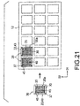
- a plurality of laminated bodies 60 and a plurality of first masks 30 are produced.
- Each first mask 30 has one opening 35, and each laminated body 60 has a size corresponding to the one opening 35 of the first mask 30.
- each laminated body 60 and each first mask 30 are subjected to the aforementioned joint step and the separation step.
- one laminated body 60 is aligned with the first mask 30 and is joined to the first mask 30.
- the laminated body 60 can be joined to the first mask 30 similarly to the aforementioned joint step.
- a substrate 51 of each laminated body 60 is separated from a metal layer 42.
- one deposition mask 20 is produced. By repeating these step plural times, a plurality of the deposition masks 20 are produced.
- the respective deposition masks 20 are stretched, and are aligned with respective openings of a frame 12 shown in Fig. 21 , for example, which has a grid-like plane shape, and are attached thereto, so as to manufacture a deposition mask 10 shown in Fig. 22 .
- Figs. 23 and 24 are views for describing yet another modification example of the manufacturing method of the deposition mask apparatus 10.
- Figs. 23 and 24 are plan views of respective members to show the respective steps of the deposition mask apparatus 10 in this modification example.
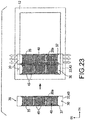
- each deposition mask 20 includes a first mask 30 having a plurality of openings 35 arranged along one direction (second direction D2), and has a general stick-like plane shape extending in the one direction.
- the respective deposition masks 20 are stretched and respectively attached to a frame 12 shown in Fig. 3 , for example, so as to manufacture a deposition mask apparatus 10 shown in Fig. 24 .
- the deposition mask 20 can be attached to the frame 12 similarly to the aforementioned attachment step.
- the deposition mask 20 having a stick-like plane shape can be stretched along the longitudinal direction (second direction D2), with only respective longitudinal ends of the deposition mask 20 being held by a plurality of clamps.
- the stretching step since the positions of the respective through-holes 45 can be corrected by stretching the deposition mask 20 along the longitudinal direction thereof, the stretching step can be facilitated.
- a notch and a joint piece which are similar to the notch 46 and the joint piece 48 described with reference to Figs. 6a and 7 , can be provided on the outer edges of the second masks 40 of the respective deposition masks 20.
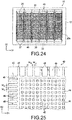
- Fig. 25 is a partial plan view showing a modification example of the second mask 40 of the deposition mask 20.
- a plurality of notches 46 are arranged along a long side of the second mask 40 (along the first direction D1), and a width W 11 of each notch 46 along the long side is larger than the first width W 1 of the notch 46 in the embodiment described above with reference to Fig. 6 .
- the plurality of notches 46 and the joint pieces 48 arranged along the long side of the second mask 40 (along the first direction D1) have the width W 11 and a width W 12 , respectively.
- the plurality of notches 46 and the joint pieces 48 arranged along a short side of the second mask 40 (along the second direction D2) have a width W 11 and a width W 21 , respectively.
- the width W 11 is larger than the width W 21 .
- the width W 12 and the width W 22 may be the same with each other.
- a residual stress (internal stress) is generated in the metal layer 42, which results in a tensile force in the plane of the metal layer 42.
- a power of the tensile force varies depending on a thickness and/or a composition of the metal layer.
- a thickness of the joint piece 48 of the second mask 40 is set to be larger than a thickness of the porous area 44, in order to ensure an appropriate joint property.
- a larger in-plane tensile force may be generated in the joint piece 48 than in the porous area 44.
- the in-plane tensile force of the joint piece 48 can be reduced, whereby lowering of positional precision of the through-holes 45 in the porous area 44, which is caused by the in-plane tensile force, can be effectively prevented.
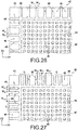
- Fig. 26 is a partial plan view showing another modification example of the second mask 40.
- a plurality of notches 46 are arranged along a long side of the second mask 40 (along the first direction D1), and a width W 11 of each notch 46 along the long side is larger than the first width W 1 of the notch 46 in the embodiment described above with reference to Fig. 6 .
- a plurality of notches 46 are arranged along a short side of the second mask 40 (along the second direction D2), and a width W 21 of each notch 46 along the short side is larger than the first width W 1 of the notch 46 in the embodiment described above with reference to Fig. 6 .
- the width W 11 and the width W 21 may be the same with each other, and the width W 12 and the width W 22 of may be the same with each other.
- Fig. 27 is a partial plan view showing yet another modification example of the second mask 40.
- a width W 112 of some notches 46 of a plurality of notches 46 arranged along a long side of the second mask 40 (along the first direction D1) is larger than a width W 111 of other notches 46.
- the width W 112 of every third notch 46 is larger than the other width W 111 of the notches 46.
- a width W 212 of some notches 46 of a plurality of notches 46 arranged along a short side of the second mask 40 (along the second direction D1) is larger than a width W 211 of other notches 46.
- the width W 212 of every third notch 46 is larger than the other width W 211 of the notches 46.
- the second mask 40 has a plurality of joint piece groups G arranged along its outer edge.
- One joint piece group G includes a plurality of joint pieces 48.
- one joint piece group G includes three joint pieces 48.
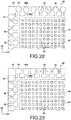
- Figs. 28 and 29 are partial plan view showing yet another modification example of the second mask 40.
- a width of a distal end 48a of a joint piece 48 is larger than a width of a proximal end 48b.
- the distal end 48 has a substantially circular outline in a plan view.
- the distal end 48a has a substantially rectangular outline in a plan view. Not limited to the substantially circular shape and the substantially rectangular shape, the distal end 48a can have any shape.
- the distal ends 48a can be joined to the first mask 30 by welding.
- the distal end 48a having relatively a larger width can ensure a suitably joint property to the first mask 30, and the proximal end 48b having relatively a smaller width can reduce the in-plane tensile force of the joint piece 48, whereby lowering of positional precision of the through-holes 45 in the porous area 44, which is caused by the in-plane tensile force, can be effectively prevented.
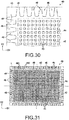
- Fig. 30 is a partial view showing yet another modification example of the second mask 40.
- a width of a joint piece 48 increases from a distal end side (end 49 side) toward a proximal end side (porous area 44 side).
- the joint piece 48 has a substantially trapezoidal outline in a plan view.
- the joint piece 48 has substantially an isosceles trapezoidal shape in a plan view.
- Fig. 31 is a plan view showing yet another modification example of the second mask 40.
- a width of a joint piece 48 increases from the distal end side of the joint piece 48 toward the proximal end side thereof.
- the plurality of joint pieces 48 arranged along a long side of the second mask 40 and the plurality of joint pieces arranged along the long side of the second mask 40 have shapes different from each other, with respect to the center of the long side.
- the plurality of joint pieces 48 arranged along a short side of the second mask 40 and the plurality of joint pieces arranged along the short side of the second mask 40 have shapes different from each other, with respect to the center of the short side.
- the joint piece 48 has a substantially trapezoidal outline in a plan view, and has an end 49 and a proximal end, which form an upper base and a lower base of the trapezoidal shape, and two side edges 481, 482, which form legs of the substantially trapezoidal shape.
- the two side edges 481, 482 include a first side edge 481 facing a corner of the second mask 40 closest from the joint piece 48, and a second side edge 482 facing away from the corner.
- An angle defined between the second side edge 482 of the joint piece 48 and the outer edge 43 of the joint piece 48, which passes the end 49, is larger than an angle defined between the first side edge 481 of the joint piece 48 and the outer edge 43 of the joint piece 48, which passes the end 49 of the joint piece 48.
- the angle defined between the side edge 481, 482 and the outer edge 43 is greater than 0 degrees and not more than 90 degrees. Particularly in the illustrated example, the angle defined between the first side edge 481 and the outer edge 43 is 90 degrees, and the angle defined between the second side edge 482 and the outer edge 43 is less than 90 degrees.
- an in-plane tensile force in the metal layer 42 precipitated by a plating method acts relatively larger along a direction connecting a center of the second mask 40 and each corner thereof (diagonal direction).
- an angle defined between an orientation in which the joint piece 48 extends from its proximal end toward its distal end, and an orientation in which an in-plane tensile force in the metal layer 42 largely acts can be made smaller.
- an in-plane tensile force acting on the porous area 44 can be prevented from becoming non-uniform.
Landscapes
- Chemical & Material Sciences (AREA)
- Engineering & Computer Science (AREA)
- Chemical Kinetics & Catalysis (AREA)
- Materials Engineering (AREA)
- Mechanical Engineering (AREA)
- Metallurgy (AREA)
- Organic Chemistry (AREA)
- Manufacturing & Machinery (AREA)
- General Chemical & Material Sciences (AREA)
- Electroluminescent Light Sources (AREA)
- Physical Vapour Deposition (AREA)
Abstract
Description
- The present disclosure relates to a deposition mask that is used for depositing a deposition material onto a substrate to be deposited (a substrate onto which the deposition material is deposited), a deposition mask apparatus, a manufacturing method of a deposition mask, and a manufacturing method of a deposition mask apparatus.
- A display device used in a portable device such as a smart phone and a tablet PC is required to have high fineness, e.g., a pixel density of not less than 400 ppi. In addition, there is increasing demand that the portable device is applicable in the ultra full high-definitions reference. In this case, the pixel density of the display device needs to be not less than 800 ppi or more, for example.
- An organic EL display device draws attention because of its excellent responsibility, low power consumption and excellent contrast. A known method for forming pixels of an organic EL display device is a method which uses a deposition mask including through-holes that are arranged in a desired pattern, and forms pixels in the desired pattern. To be specific, a substrate for an organic EL display device (substrate for organic EL) is firstly put into a deposition apparatus. Then, a deposition step in which a deposition mask is brought into contact with the substrate for organic EL so as to deposit an organic material onto the substrate for organic EL is carried out in the deposition apparatus.
- A deposition mask disclosed in
JP2016-148112A JP2016-148112A - In the technique disclosed in
JP2016-148112A - In order to solve this problem, the present inventors have worked out the manufacture of a deposition mask and a deposition mask apparatus in the following method. Firstly, for example, a conductive pattern made of a conductive material, such as copper, is provided on a substrate. A metal layer which will serve as a deposition mask is provided on the conductive pattern, so as to produce a laminated body including the substrate, the conductive pattern and the metal layer. Then, the metal layer of the laminated body is joined to a frame by welding, for example. Thereafter, the conductive pattern is etched and removed, and the substrate is separated from the metal layer. Thus, a deposition mask formed of the metal layer, and a deposition mask apparatus having the deposition mask and the frame can be manufactured. According to such a method, since the metal layer of the laminated body, which will serve as the deposition mask, is joined to the frame while the metal layer is being held on the substrate, flatness of the deposition mask can be well ensured. Thus, it is considered that the deposition mask can be prevented from being wrinkled and/or deformed.
- However, the present inventors have found the following problem in this method. When the deposition mask is a metal layer that is precipitated by using a plating method, a residual stress (internal stress) is generated in the metal layer, so that a tensile force may be generated in a plane of the metal layer. A power of the tensile force varies depending on a thickness and/or a composition of the metal layer. The deposition mask formed of a plated layer inevitably has non-uniform thickness and/or composition in its plane. In this case, the tensile force in the plane of the deposition mask may become non-uniform. Thus, in the deposition mask from which a substrate has been removed, there is a possibility that positions of respective through-holes are displaced from predetermined positions, because of the non-uniform tensile force in the plane.
- The present disclosure has been made in view of the above circumstances. The object of the present disclosure is to provide a deposition mask, a deposition mask apparatus, and a manufacturing method of a deposition mask and a deposition mask apparatus, capable of preventing positional displacement of through-holes.
- A deposition mask of the present disclosure comprises:
- a first mask having an opening formed therein; and
- a second mask superposed on the first mask and having a plurality of through-holes formed therein, the through-hole having a planar dimension smaller than a planar dimension of the opening;
- wherein:
- the deposition mask has a plurality of joints that join the second mask and the first mask to each other;
- the plurality of joints are arranged along an outer edge of the second mask; and
- a notch is formed at a position in the outer edge of the second mask, the position corresponding to a space between the adjacent two joints.
- A deposition mask of the present disclosure comprises the aforementioned deposition mask, and a frame attached to the deposition mask.
- A manufacturing method of a deposition mask of the present disclosure is a manufacturing method of a deposition mask including a first mask in which a plurality of openings arranged at least along a first direction are formed, and a second mask superposed on the first mask and having a plurality of through-holes formed therein, the through-hole having a planar dimension smaller than a planar dimension of the opening, the manufacturing method comprising:
- a joint step in which a metal layer of a laminated body is joined to the first mask by a plurality of joints, wherein the laminated body includes a substrate, a conductive pattern provided on the substrate, and the metal layer provided on the conductive pattern on the opposite side of the substrate; and
- a separation step in which the substrate is separated from the metal layer by etching and removing the conductive pattern so as to form the second mask from the metal layer.
- In the manufacturing method of a deposition mask of the present disclosure, the plurality of joints may be arranged along an outer edge of the metal layer; and a notch may be formed at a position in the outer edge of the metal layer, the position corresponding to a space between the two joints that are adjacent to each other in the arrangement direction of the plurality of joints.
- A manufacturing method of a deposition mask apparatus of the present disclosure is a manufacturing method of a deposition mask apparatus including a deposition mask and a frame attached to the deposition mask, the manufacturing method comprising:
- a preparation step in which the aforementioned deposition mask, or a deposition mask manufactured by the aforementioned manufacturing method of a deposition mask, is prepared; and
- an attachment step in which the deposition mask is attached to a frame.
- The manufacturing method of a deposition mask apparatus of the present disclosure may further comprises, , before the attachment step, a stretching step in which the deposition mask is stretched in a planar direction thereof.
- The present disclosure can provide a deposition mask, a deposition mask apparatus, and a manufacturing method of a deposition mask and a deposition mask apparatus, capable of restraining positional displacement of through-holes.
-
-
Fig. 1 is a view for describing an embodiment of the present disclosure, which describes a deposition apparatus having a deposition mask apparatus, and a deposition method using the deposition apparatus. -
Fig. 2 is a cross-sectional view showing an example of an organic EL display device manufactured by the deposition apparatus shown inFig. 1 . -
Fig. 3 is a plan view schematically showing the deposition mask apparatus having the deposition mask. -
Fig. 4 is a cross-sectional view of the deposition mask apparatus corresponding to a IV-IV line inFig. 3 . -
Fig. 5 is a plan view showing an example of a first mask of the deposition mask. -
Fig. 6 is a plan view showing an example of a second mask of the deposition mask. -
Fig. 7 is a partial plan view of the deposition mask apparatus, showing a part indicated by VII inFig. 3 , which is seen from a second surface side of the deposition mask. -
Fig. 8 is a view showing a step of an example of a manufacturing method of the deposition mask. -
Fig. 9 is a view showing a step of an example of a manufacturing method of the deposition mask. -
Fig. 10 is a view showing a step of an example of a manufacturing method of the deposition mask. -
Fig. 11 is a view showing a step of an example of a manufacturing method of the deposition mask. -
Fig. 12 is a view showing a step of an example of a manufacturing method of the deposition mask. -
Fig. 13 is a view showing a step of an example of a manufacturing method of the deposition mask apparatus. -
Fig. 14 is a view showing a step of an example of a manufacturing method of the deposition mask apparatus. -
Fig. 15 is a view showing a step of an example of a manufacturing method of the deposition mask apparatus. -
Fig. 16 is a view showing a step of a modification example of a manufacturing method of the deposition mask apparatus. -
Fig. 17 is a view showing a step of a modification example of a manufacturing method of the deposition mask apparatus. -
Fig. 18 is a view showing a step of another modification example of a manufacturing method of the deposition mask apparatus. -
Fig. 19 is a view showing a step of another modification example of a manufacturing method of the deposition mask apparatus. -
Fig. 20 is a view showing a step of yet another modification example of a manufacturing method of the deposition mask apparatus. -
Fig. 21 is a view showing a step of yet another modification example of a manufacturing method of the deposition mask apparatus. -
Fig. 22 is a view showing a step of yet another modification example of a manufacturing method of the deposition mask apparatus. -
Fig. 23 is a view showing a step of yet another modification example of a manufacturing method of the deposition mask apparatus. -
Fig. 24 is a view showing a step of yet another modification example of a manufacturing method of the deposition mask apparatus. -
Fig. 25 is a partial plan view showing a modification example of a second mask. -
Fig. 26 is a partial plan view of another modification example of the second mask. -
Fig. 27 is a partial plan view of yet another modification example of the second mask. -
Fig. 28 is a partial plan view of yet another modification example of the second mask. -
Fig. 29 is a partial plan view of yet another modification example of the second mask. -
Fig. 30 is a partial plan view of yet another modification example of the second mask. -
Fig. 31 is a plan view of yet another modification example of the second mask. - The below-described embodiments are examples of the embodiment of the present disclosure, and the present disclosure should not be limited to the embodiments.
- An embodiment of the present disclosure is described with reference to the drawings. In the drawings attached to the specification, a scale dimension, an aspect ratio and so on are changed and exaggerated from the actual ones, for the convenience of easiness in illustration and understanding.
-
Figs. 1 to 31 are views for describing an embodiment of the present disclosure. In the below embodiment, a deposition mask apparatus used for patterning an organic material on a substrate in a desired pattern in order to manufacture an organic EL display device, and a manufacturing method of the deposition mask apparatus are described by way of example. However, the present disclosure is not limited to this application, and can be applied to a deposition mask apparatus used for various purposes and a manufacturing method of the deposition mask apparatus. - In this specification, the terms "plate", "sheet" and "film" are not differentiated from one another, based only on the difference in terms. For example, the "plate" is a concept including a member that can be referred to as "sheet" or "film".
- In addition, the term "plate plane (sheet plane, film plane)" means a plane corresponding to a plane direction of a plate-like (sheet-like, film-like) member as a target, when the plate-like (sheet-like, film-like) member as a target is seen as a whole in general. A planar direction used for a plate-like (sheet-like, film-like) member means a direction parallel to a plate plane (sheet plane, film plane) of the member. In addition, a normal direction used to the plate-like (sheet-like, film-like) member means a normal direction with respect to a plate plane (sheet surface, film surface) of the member.
- Further, the terms used herein specifying shapes, geometric conditions, physical properties, and their degrees, e.g., "parallel," "perpendicular," "same," "similar" etc., and values of lengths and angles as well as physical properties are not limited to their strict definitions, but construed to include a range capable of exerting a similar function.
- Firstly, a deposition apparatus 90 for performing a deposition process for depositing a deposition material onto an object is explained with reference to
Fig. 1 . As shown inFig. 1 , the deposition apparatus 90 includes therein a deposition source (e.g., a crucible 94), aheater 96, and adeposition mask apparatus 10. In addition, the deposition apparatus 90 may further include exhaust means to create a vacuum atmosphere inside of the deposition apparatus 90. The crucible 94 accommodates adeposition material 98 such as an organic luminescent material. Theheater 96 is configured to heat the crucible 94 so as to evaporate thedeposition material 98 in the vacuum atmosphere. Thedeposition mask apparatus 10 is located opposite to the crucible 94. - As shown in
Fig. 1 , thedeposition mask apparatus 10 includes adeposition mask 20 and aframe 12 for supporting thedeposition mask 20. Theframe 12 is configured to support thedeposition mask 20 to pull it in a taut state in its planar direction in order to prevent thedeposition mask 20 from warping. As shown inFig. 1 , thedeposition mask apparatus 10 is disposed in the deposition apparatus 90 such that thedeposition mask 20 faces a substrate to be deposited (e.g., an substrate for organic EL) 92, which is an object onto which thedeposition material 98 is to be deposited. - As shown in
Fig. 1 , thedeposition mask apparatus 10 may include amagnet 93 disposed on a surface of the substrate fororganic EL 92, which is opposite to the surface on thedeposition mask 20 side. By providing themagnet 93, thedeposition mask 20 can be attracted to themagnet 93 by magnetic force, so that thedeposition mask 20 can be brought into tight contact with the substrate to be deposited 92. - As shown in
Fig. 1 , thedeposition mask 20 includes afirst mask 30 and asecond mask 40 superposed on thefirst mask 30. Thefirst mask 30 has aplate member 32 and a plurality ofopenings 35 formed in theplate member 32. In addition, thesecond mask 40 has ametal layer 42 and a plurality of through-holes 45 formed in themetal layer 42. For example, a thickness of thefirst mask 30 is not less than 50 µm and not more than 3000 µm, and a thickness of thesecond mask 40 is not less than 2.5 µm and not more than 30 µm. The through-hole 45 has a planar dimension smaller than a planar dimension of theopening 35. The description that the through-hole 45 has a planar dimension smaller than a planar dimension of theopening 35 means that the dimension of the through-hole 45 is smaller than the dimension of theopening 35 in all the directions along a plate plane of the first mask 30 (a plate plane of the second mask 40). Thus, in the example shown inFigs. 3 and7 , in a plan view, an outline delimiting theopening 35 surrounds outlines delimiting the through-holes 45 positioned in theopening 35. A maximum dimension of the through-hole 45 in the planar direction is not less than 5 µm and not more than 100 µm, for example. The through-hole 45 of thesecond mask 45 is also formed at a position that is not overlapped with theopening 35 of thefirst mask 30. In a plan view, the through-hole 45 may have a slit-like shape having a longitudinal direction and a width direction orthogonal to the longitudinal direction. In this case, a maximum width of the through-hole 45 along the width direction may be not less than 5 µm and not more than 100 µm, for example. - As shown in
Fig. 1 , thedeposition mask 20 has afirst surface 20a and asecond surface 20b that defines a surface opposite to thefirst surface 20a. In the illustrated example, thedeposition mask 20 is disposed between the substrate to be deposited 92 and the crucible 94. Thedeposition mask 20 is supported in the deposition apparatus 90 such that itssecond surface 20b faces a lower surface of the substrate to be deposited 92, in other words, such that itsfirst surface 20a faces the crucible 94, and is used for depositing thedeposition material 98 onto the substrate to be deposited 92. In the deposition apparatus 90 shown inFig. 1 , thedeposition material 98 evaporated from the crucible 94 to reach thedeposition mask 20 from thefirst surface 20a side adheres to the substrate to be deposited 92 through theopenings 35 of thefirst mask 30 and the through-holes 45 of thesecond mask 40. Thus, thedeposition material 98 can be film-deposited onto the surface of the substrate to be deposited 92 in a desired pattern corresponding to the positions of theopenings 35 of thefirst make 30 and the through-holes 45 of thesecond mask 40. -
Fig. 2 is a cross-sectional view showing an organicEL display device 100 manufactured by using the deposition apparatus 90 ofFig. 1 . The organicEL display device 100 includes the substrate to be deposited (substrate for organic EL) 92 and patterned pixels containing thedeposition materials 98. - When a color display is desired with a plurality of colors, deposition apparatuses 90 equipped with
deposition masks 20 corresponding to the respective colors are prepared, and the substrate to be deposited 92 is introduced into each deposition apparatus 90. Accordingly, for example, an organic luminescent material for red color, an organic luminescent material for green color, and an organic luminescent material for blue color can be sequentially deposited on the substrate to be deposited 92. - The deposition process is sometimes performed inside the deposition apparatus 90 in a high-temperature atmosphere. In this case, during the deposition process, the
deposition mask 20, theframe 12, and the substrate to be deposited 92, which are held inside the deposition apparatus 90, are also heated. At this time, thefirst mask 30 and thesecond mask 40 ofdeposition mask 20, theframe 12, and the substrate to be deposited 92 develop dimensional change behaviors based on their respective thermal expansion coefficients. In this case, when the thermal expansion coefficients of thefirst mask 30, thesecond mask 40, theframe 12 and the substrate to be deposited 92 largely differ from one another, positioning displacement occurs because of the difference in dimensional change. As a result, dimensional precision and/or positional precision of the deposition material deposited onto the substrate to be deposited 92 decrease. - In order to solve this problem, the thermal expansion coefficients of the
first mask 30, thesecond mask 40 and theframe 12 are preferably equivalent to the thermal expansion coefficient of the substrate to be deposited 92. For example, when a glass substrate is used as the substrate to be deposited 92, an iron alloy containing nickel can be used as a main material of thefirst mask 30, thesecond mask 40 and theframe 12. For example, it is possible to use, as a material for forming thefirs mask 30, thesecond mask 40 and theframe 12, an iron alloy containing not less than 30% by mass and not more than 54% by mass of nickel. Specific examples of an iron alloy containing nickel may be an invar material containing not less than 34% by mass and not more than 38% by mass of nickel, a super invar material containing cobalt in addition to not less than 30% by mass and not more than 34% by mass of nickel, and a low thermal expansion Fe-Ni based plated alloy not less than 38% by mass and not more than 54% by mass of nickel. - When the temperatures of the
first mask 30, thesecond mask 40, theframe 12 and the substrate to be deposited 92 do not reach high temperatures during the deposition process, it is not necessary that the thermal expansion coefficients of thefirst mask 30, thesecond mask 40 and theframe 12 are equivalent to the thermal expansion coefficient of the substrate to be deposited 92. In this case, a material other than the aforementioned iron alloy may be used as the material forming thefirst mask 30 and thesecond mask 40. For example, an alloy other than the aforementioned iron alloy containing nickel, such as an iron alloy containing chromium, may be used. As an iron alloy containing chromium, for example, an iron alloy, which is called so-called stainless steel, can be used. In addition, alloys such as a nickel or nickel-cobalt alloy other than iron alloys may be used. - Next, the
deposition mask apparatus 10 and thedeposition mask 20 are described in detail with reference toFigs. 1 and3 to 7 .Fig. 3 is a plan view schematically showing an example of thedeposition mask apparatus 10 having thedeposition mask 20, thedeposition mask apparatus 10 being seen from thefirst surface 20 side.Fig. 4 is a cross-sectional view of thedeposition mask apparatus 10, which shows thedeposition mask 10 in a cross-section corresponding to a VI-VI line ofFig. 3 . - In the example shown in
Fig. 3 , thedeposition mask 20 has an outline of, for example, a substantially quadrangular shape in a plan view, more precisely, a substantially rectangular shape in a plan view. Theframe 12 is formed as a substantially rectangular frame. Thedeposition mask 20 is attached to theframe 12 such that each side of thedeposition mask 20 corresponds to each side of theframe 12. - The
deposition mask 20 has thefirst mask 30 and thesecond mask 40 stacked on each other. In the example shown inFigs. 1 ,3 and 4 , thesecond mask 40 is disposed on thesecond surface 20b side with respect to thefirst mask 30. Thus, the surface of thefirst mask 30, which is opposite to thesecond mask 40, and the surface of thesecond mask 40, which is exposed from theopening 35 of thefirst mask 30, define thefirst surface 20a of thedeposition mask 20. The surface of thesecond mask 40, which is opposed to thefirst mask 30, defines thesecond surface 20b of thedeposition mask 20. In the illustrated example, thefirst mask 30 and thesecond mask 40 respectively have a substantially rectangular outline in a plan view. Particularly in the illustrated example, thefirst mask 30 has a planar dimension larger than a planar dimension of thesecond mask 40. In a plan view, the outline delimiting thefirst mask 30 surrounds the outline delimiting thesecond mask 40. - The
first mask 30 and thesecond mask 40 of thedeposition mask 20 are fixed to each other. To this end, thedeposition mask 20 has a plurality offirst joints 16 that join thefirst mask 30 and thesecond mask 40 to each other. In addition, thefirst mask 30 and theframe 12 are fixed to each other. To this end, thedeposition mask apparatus 10 has a plurality ofsecond joints 18 that join thefirst mask 30 and theframe 12 to each other. Thejoints outer edge 22 of thedeposition mask 20. Particularly in the illustrated example, theouter edge 22 of thedeposition mask 20 and anouter edge 43 of thesecond mask 40 extend parallel to each other, i.e., along the same direction. As described above, in the illustrated example, thedeposition mask 20 has the substantially rectangular outline in a plan view. Thus, thejoints outer edge 22 of thedeposition mask 20. In the example shown inFig. 7 , thejoints outer edge 22 of thedeposition mask 20. Namely, thejoints outer edge 22 of thedeposition mask 20 extends. In addition, in the illustrated example, thejoints outer edge 22 extends. In this specification, the description that thejoints outer edges joints outer edges joints outer edges joints outer edges first mask 30 and thesecond mask 40 are fixed to each other by spot welding. Thus, the respectivefirst joints 16 and thesecond joints 18 are formed as joints by spot welding. However, not limited thereto, thefirst mask 30 and thesecond mask 40, and/or thefirst mask 30 and theframe 12 may be fixed to each other by another fixing means such as an adhesive. Namely, the respectivefirst joints 16 and thesecond joints 18 may be formed as adhesive parts. - Next, the
first mask 30 is described.Fig. 5 is a plan view showing thefirst mask 30 of thedeposition mask apparatus 10 ofFig. 3 . In the illustrated example, thefirst mask 30 has the plurality ofopenings 35 which are arranged at predetermined pitches along a first direction D1 and a second direction D2. The first direction D1 and the second direction D2 are directions both parallel to a plane direction of theplate member 32 of thefirst mask 30. In addition, the second direction D2 is orthogonal to the first direction D1. In this embodiment, thefirst mask 30 having a single layer is described by way of example. However, not limited thereto, thefirst mask 30 may have a plurality of layers. Namely, thefirst mask 30 may be produced by laminating a plurality of layers along its plate plane direction. - One
opening 35 of thefirst mask 30 corresponds to one display area of the organicEL display device 100. Therefore, the illustrateddeposition mask apparatus 10 enables a multifaceted deposition of the organicEL display device 100, correspondingly to therespective openings 35 of thefirst mask 30. - As shown in
Figs. 3 and5 , theopening 35 has an outline of, for example, a substantially quadrangular shape in a plan view, more precisely, a substantially rectangular shape in a plan view. However, although not shown, each opening 35 can have an outline of a different shape in accordance with the shape of the display area of the substrate to be deposited (substrate for organic EL) 92. For example, each opening 35 may have a circular outline.Fig. 3 shows that therespective openings 35 have the same shape with each outer in a plan view. However, not limited thereto, therespective openings 35 may have opening shapes different from one another. In other words, thefirst mask 30 may have a plurality ofopenings 35 having different shapes in a plan view. - In the illustrated example, an
alignment mark 37 is provided near a corner of each opening 35 of thefirst mask 30. In particular, oneopening 35 is provided, correspondingly to four corners thereof, with four alignment marks 37. In the illustrated example, some (e.g., two) alignment marks 37 are shared by theopenings 35 adjacent to each other. The alignment marks 37 are used when relative positions between the respective through-holes 45 of thesecond mask 40 exposed into therespective opening 35 are aligned with predetermined positions, in a stretching step performed in a manufacturing method of thedeposition mask apparatus 10 described later. A specific shape of thealignment mark 37 is not specifically limited, as long as it can be recognized by an imaging device such as a camera. Alignment of the through-holes 45 using these alignment marks 37 can be carried out similarly to the method described inJP4606114B2 JP4562488B2 - Next, the
second mask 40 is described.Fig. 6 is a plan view showing thesecond mask 40 of thedeposition mask apparatus 10 ofFig. 3 . As shown inFig. 6 , the plurality of through-holes 45 of thesecond mask 40 are formed over the whole area of aporous area 44 including an area overlapping with the plurality ofopenings 35 of thefirst mask 30. The example shown inFig. 6 can make uniform rigidity of thesecond mask 40 and an internal stress (residual stress) generated in thesecond mask 40, as compared with a case in which the through-holes 45 are provided in only a part corresponding to a display area of the substrate to be deposited (substrate for organic EL) 92. Thus, it can be prevented that irregularities such as wrinkles are generated in thesecond mask 40 because of the non-uniform rigidity and/or internal stress. There may be an area in which no through-hole 45 is formed outside theporous area 44 of themetal layer 42 of thesecond mask 40. - Returning to
Fig. 1 , a through-hole 45 of the through-holes 45 of thesecond mask 40, which is not overlapped with theopening 35 of thefirst mask 30, is covered by aplate member 32 of thefirst mask 30 from thefirst surface 20a side of thedeposition mask 20. In this case, thedeposition material 98, which flies from the deposition source positioned on thefirst surface 20a side with respect to thedeposition mask 20, reaches the substrate to be deposited 92 through a through-hole 45 of the through-holes 45 of thesecond mask 40, which is overlapped with theopening 35 of thefirst mask 30. - Herebelow, an example of a specific shape of the
deposition mask apparatus 10, in particular, a specific shape of thesecond mask 40, is described in detail with reference mainly toFig. 7. Fig. 7 is a partial plan view of thedeposition mask apparatus 10, showing a part surrounded by one-dot chain lines indicted by VII ofFig. 3 , which is seen from thesecond surface 20b side of thedeposition mask 20. - In the example shown in
Fig. 7 , the through-hole 45 has has an outline of, for example, a substantially quadrangular shape in a plan view, more precisely, a substantially rectangular shape in a plan view. However, although not shown, each through-hole 45 can have an outline of a different shape in accordance with the shape of the pixel of the organicEL display device 100. For example, each through-hole 45 may have a circular outline or a slit-like outline. - A
notch 46 is formed at a position in theouter edge 43 of thesecond mask 40, the position corresponding to a space between the adjacent twofirst joints 16. Herein, the position in theouter edge 43 of thesecond mask 40, the position corresponding to a space between the adjacent twofirst joints 16, indicates a part of theouter edge 22, which is positioned from a position between the adjacent twofirst joints 16 in a direction orthogonal to a direction connecting the adjacent twofirst joints 16 in the plate plane of thesecond mask 40. Particularly in the example shown inFigs. 6 and7 , thenotch 46 is formed in theouter edge 43 of thesecond mask 43 to include a position corresponding to a center between the adjacent twofirst joints 16. Namely, thenotch 46 is formed to include a part of theouter edge 22, which is positioned from a position at a center between the adjacent twofirst joints 16 in a direction orthogonal to a direction connecting the adjacent twofirst joints 16 in the plate plane of thesecond mask 40. - Since the
second mask 40 hassuch notches 46, an etchant can penetrate from theouter edge 43 side of thesecond mask 40 through thenotches 46, in a separation step of the manufacturing method of thedeposition mask 20 described later. Thus, aconductive pattern 52 located near theouter edge 43 can be easily etched and removed. - Each
notch 46 extends from theouter edge 43 of thesecond mask 40 toward theporous area 44. In the example shown inFigs. 6 and7 , thenotch 46 has a certain width and extends from theouter edge 43 of thesecond mask 40 toward theporous area 44. In the illustrated example, corners of an end of thenotch 46 on theporous area 44 side are rounded. In particular, the end of thenotch 46 on theporous area 44 side has a substantially semicircular shape. Thus, when an external force is applied to thesecond mask 40, it can be prevented that a stress is concentrated on a certain area in thenotch 46 so that the area is cracked and/or deformed. - A
joint piece 48 is formed between the adjacent twonotches 46. In other words, thejoint piece 48 is positioned between the adjacent twonotches 46. Thesecond mask 40 is joined to thefirst mask 30 at thejoint piece 48. Namely, thejoint piece 48 and thefirst mask 30 are fixed to each other through the first joint 16. In the example shown inFigs. 6 and7 , one first joint 16 is located on onejoint piece 48. In the illustrated example, a plurality ofjoint pieces 48 is arranged along theouter edge 43 of thesecond mask 40. The plurality ofjoint pieces 48 are equidistantly arranged along a direction in which theouter edge 22 extends. - Each
joint piece 48 extends from theouter edge 43 of thesecond mask 40 toward theporous area 44 in a plan view. In the example shown inFigs. 6 and7 , thejoint piece 48 has a certain width, excluding a part of its area on theporous area 44 side, and extends from theouter edge 43 of thesecond mask 40 toward theporous area 44. - In the illustrated example, each
joint piece 48 is disposed on an outermost circumference of thesecond mask 40. Anend 49, which is positioned on the opposite side of theporous area 44 along the direction in which eachjoint piece 48 extends, defines a part of theouter edge 43 of thesecond mask 40. Thus, in this embodiment, a substantially rectangular virtual line formed by connecting the respective ends 49 of the plurality ofjoint pieces 48 defines theouter edge 43 of thesecond mask 40. - In the
outer edge 43 of thesecond mask 40, thenotch 46 has a first width W1 along the direction in which the outer edge extends. In addition, thejoint piece 48 has a second width W2 along the direction in which theouter edge 22 extends. In this embodiment, the first width W1 of thenotch 46 is larger than the second width W2 of thejoint piece 48. Thus, in the separation step of the manufacturing method of the deposition mask described later, an etchant can penetrate from theouter edge 43 side of thesecond mask 40 through thenotch 46 having the first width W1 that is larger than the second width W2 of thejoint piece 48. Thus, theconductive pattern 52 located near theouter edge 43 can be more easily etched and removed. The first width W1 of thenotch 46 may be not less than 1 mm and not more than 10 mm, for example. The second width W2 of of thejoint piece 48 may be not less than 1 mm and not more than 3 mm, for example. In addition, a length L of the joint piece 48 (a length of the notch 46) may be not less than 1 mm and not more than 5 mm, for example. - Next, an example of the manufacturing method of the
deposition mask 20 is described with reference toFigs. 8 to 12. Figs. 8 to 12 are cross-sectional views of respective members to show examples of respective steps of thedeposition mask 20. - Firstly, an example of a method of producing a
pattern substrate 50 used for manufacturing the vapordeposition mask apparatus 10 is described. Asubstrate 51 is firstly prepared. A material forming thesubstrate 51 and a thickness of thesubstrate 51 are not specifically limited, as long as they offer an insulation property and a suitable strength. As described below, when thefirst mask 30 and thesecond mask 40 are welded and fixed by laser beam irradiation through thesubstrate 51, a glass material having a high light transmissivity can be suitably used as a material forming thesubstrate 51. - Then, a
conductive pattern 52 is formed on one surface of thesubstrate 51. In the illustrated example, theconductive pattern 52 has a pattern corresponding to a pattern of thesecond mask 40 to be formed in the below-described film deposition step. For example, theconductive pattern 52 has the same pattern as the pattern of thesecond mask 40 to be formed in the below-described film deposition step. A conductive material such as a metal material or an oxide conductive material is suitably used as a material forming theconductive pattern 52. For example, a metal material may be chromium or copper. Preferably, a material having a high bonding property to the below-described covering layer is used as a material forming theconductive pattern 52. For example, when the covering layer is produced by patterning a so-called dry film, such as a resist film containing an acryl-based photosetting resin, copper is preferably used as a material forming theconductive pattern 52. - The
conductive pattern 52 may be formed by removing by etching, for example, a part of the conductive layer disposed on thesubstrate 51, which is other than a part for defining theconductive pattern 52. In more detail, a conductive layer formed of the aforementioned conductive material is firstly provided on thesubstrate 51 by sputtering or electroless plating. Then, a covering layer having a predetermined pattern is formed on the conductive layer. A photolithographic method may be employed as a method for forming the covering layer. Thereafter, a part of the conductive layer, which is not covered with the covering layer, is removed by etching, and then the covering layer is removed. Thus, as shown inFig. 8 , thepattern substrate 50 on which theconductive pattern 52 having the pattern corresponding to thesecond mask 40 is formed can be obtained. A thickness of the conductive pattern 52 (a thickness of the conductive layer) may be not less than 50 nm and not more than 300 nm, for example. - Then, a film deposition step in which a
metal layer 42 is formed on theconductive pattern 52 is performed. In the film deposition step, ametal layer 42 provided with through-holes 45 is formed on theconductive pattern 52. To be specific, a plating step in which a plating solution is supplied onto thesubstrate 51 on which theconductive pattern 52 is formed so as to precipitate themetal layer 42 on theconducive pattern 52, is performed. For example, thesubstrate 51 on which theconductive pattern 52 is formed is immersed into a plating bath filled with a plating solution. Thus, as shown inFig. 9 , themetal layer 42 which will become thesecond mask 40 can be formed on theconductive pattern 52. - A specific method of the plating step is not particularly limited, as long as the
metal layer 42 can be precipitated on theconductive pattern 52. For example, the plating step may be performed as a so-called electrolytic plating step in which a current is applied to theconductive pattern 52 so as to precipitate themetal layer 42 on theconductive pattern 52. Alternatively, the plating step may be an electroless plating step. When the plating step is an electroless plating step, a suitable catalyst layer may be provided on theconductive pattern 52. Also when an electrolytic plating step is performed, a catalyst layer may be provided on theconductive pattern 52. - Ingredients of the plating solution to be used are suitably determined in accordance with properties required for the
metal layer 42. For example, as the plating solution, a mixed solution containing nickel sulfamate or nickel bromide and a solution containing ferrous sulfamate may be used. The plating solution may contain various additives. Examples of additives that can be used include pH buffers such as boric acid, primary brighteners such as saccharin sodium, secondary brighteners such as butynediol, propargyl alcohol, coumarin, formalin and thiourea, and antioxidants. - By this film deposition step, a
laminated body 60 having thepattern substrate 50 and themetal layer 42, as shown inFig. 9 , can be produced. In the illustrated example, thelaminated body 60 has thesubstrate 51, theconductive pattern 52 provided on thesubstrate 51, and themetal layer 42 provided on theconductive pattern 52 on the opposite side of thesubstrate 51. After the film deposition step, thelaminated body 60 may be cut at a position which will become theouter edge 43 of thesecond mask 40. - Then, a joint step in which the
first mask 30 and themetal layer 42 are joined to each other is performed. In the joint step, themetal layer 42 of thelaminated body 60 is joined to thefirst mask 30 by a plurality of first joints (joints) 16. Particularly in this embodiment, thejoint pieces 48 in themetal layer 42 are joined to thefirst mask 30. For example, spot welding may be employed as the joint method. In the example shown inFig. 10 , thefirst mask 30 and themetal layer 42 are fixed to each other by laser spot welding. - In the example shown in
Fig. 10 , thefirst mask 30 is superposed on themetal layer 42 such that thefirst mask 30 in which a plurality of openings are formed and themetal layer 42 are in contact with each other. In this embodiment, as well shown inFigs. 3 and7 , theouter edge 33 of thefirst mask 30 is positioned outside theouter edge 43 of the metal layer 42 (the outer edge of the second mask 40) in the planar direction. Then, thejoint piece 48 of themetal layer 42 is irradiated with a laser beam L1 from thesubstrate 51 side through thesubstrate 51 to melt a part of thejoint piece 48 and a part of thefirst mask 30 by heat generated by the irradiation of the laser beam L1, so that thejoint piece 48 and thefirst mask 30 are welded and fixed. At this time, as shown inFig. 11 , a first joint 16 made of the parts of thefirst mask 30 and themetal layer 42, which have been melted and then solidified, is formed across thejoint piece 48 and thefirst mask 30. Namely, thefirst mask 30 and themetal layer 42 are joined to each other through the first joint 16. At this time, since the thickness of the metal layer 42 (second mask 40) and the thickness of theconductive pattern 52 are smaller than the thickness of thefirst mask 30, themetal layer 42 and thefirst mask 30 can be joined in a short period of time with less energy, by applying the laser beam L1 from thesubstrate side 51, i.e., from themetal layer 42 side with respect to thefirst mask 30. - For example, a YAG laser beam generated by a YAG laser system can be used as the laser beam L1. For example, as a YAG laser system, a system including a crystal of YAG (yttrium aluminum garnet) doped with Nd (neodymium) as an oscillation medium can be used.
- In this manner, by joining the
first mask 30 and themetal layer 42 to each other while themetal layer 42 is being supported on thesubstrate 51, flatness of themetal layer 42 can be well ensured. Thus, generation of wrinkles and/or deformation of themetal layer 42 can be prevented. In the joint step, thefirst mask 30 and themetal layer 42 may be joined while a circumference of thefirst mask 30 is being pulled, i.e., stretched outside in an in-plane direction. In this case, after the separation step described later, it can be prevented that thefirst mask 30 is deformed by a residual stress in themetal layer 42 so that thedeposition mask 20 is deformed as a whole. - Then, a separation step in which a combined body of the
first mask 30 and themetal layer 42 is separated from thesubstrate 51 is performed. In the separation step, the combined body is firstly immersed into an etchant capable of selectively etching theconductive pattern 52. Then, the combined body is peeled and separated from thesubstrate 51. Thereafter, the combined body is again immersed into the etchant so as to completely etch and remove theconductive pattern 52 remaining on themetal layer 42. Thus, thesubstrate 51 is separated from themetal layer 42, so that asecond mask 40 can be formed from themetal layer 42. - In the example shown in
Fig. 11 , theconductive pattern 52 positioned in theopening 35 of thefirst mask 30 in a plan view is exposed into the through-holes 45 of thesecond mask 40. Thus, theconductive pattern 52 is etched by the etchant having penetrated into the through-hole 45 from a surface exposed into the through-hole 45, i.e., a side surface. In the illustrated example, the etching proceeds from the side surface of theconductive pattern 52 to the inside. Thus, themetal layer 42 of thesecond mask 40 and thesubstrate 51 are separated. - In addition, in the separation step, the etchant penetrates into the
notch 46 from theouter edge 43 side of thesecond mask 40. Theconductive pattern 52 present between thejoint piece 48 and thesubstrate 51 is exposed into thenotch 46. Thus, theconductive pattern 52 is etched by the etchant having penetrated into thenotch 46 from a surface exposed into thenotch 46, i.e., the side surface. By using as the etchant an etchant that does not dissolve thefirst mask 30 and thesecond mask 40 but dissolves only theconductive pattern 51, only theconductive pattern 52 can be dissolved and removed, without thefirst mask 30 and thesecond mask 40 being eroded by the etchant. The etching proceeds from the side surface of theconductive pattern 52, which corresponds to opposed side surfaces of thepoint piece 48, to the inside. Thus, themetal layer 42 of thesecond mas 40 and thesubstrate 51 are separated. - In the step of etching and removing the
conductive pattern 52, the metal layer 42 (second mask 40) and thesubstrate 51 may not be completely separated. Namely, themetal layer 42 and thesubstrate 51 may be connected partially by theconductive pattern 52. In this case, by peeling thesubstrate 51 from the combined body of thefirst mask 30 and thesecond mask 40 to break theconductive pattern 52 which partially connects themetal layer 42 and thesubstrate 51, thesubstrate 51 can be separated from the combined body. Theconductive pattern 52 remaining on themetal layer 42 can be completely etched and removed by again immersing the combined body into the etchant. - By these steps, the
deposition mask 20 having thefirst mask 30 and thesecond mask 40, as shown inFig. 12 , can be obtained. - Next, an example of the manufacturing method of the
deposition mask apparatus 10 is described with reference toFigs. 13 and14 .Fig. 13 is a plan view showing thedeposition mask 20 and theframe 12, in particular, showing thedeposition mask 20 seen from thefirst surface 20a side.Fig. 14 is a cross-sectional view showing thedeposition mask 20 and theframe 12. - Firstly, the
deposition mask 20, which is manufactured by the manufacturing method described above with reference toFigs. 8 to 12 , is prepared. - Then, a stretching step in which tension is given to the
deposition mask 20 in the planar direction, i.e., thedeposition mask 20 is stretched in its planar direction, is performed. As shown inFig. 13 , the respective sides of therectangular deposition mask 20 are held by a plurality of clamps, not shown, and the respective clamps are pulled outside in the planar direction with respect to thedeposition mask 20, so that thedeposition mask 20 is stretched. - Since the
metal layer 42 of thesecond mask 40 is a metal layer precipitated by a plating method, a residual stress (internal stress) is generated in themetal layer 42, which results in a tensile force in the plane of themetal layer 42. A power of the tensile force varies depending on a thickness and/or a composition of themetal layer 42. Themetal layer 42 formed of a plated layer inevitably has non-uniform thickness and/or composition in its plane. In this case, the tensile force in the plane of themetal layer 42 may become non-uniform. Thus, in themetal layer 42 from which thesubstrate 51 has been removed, there is a possibility that positions of the respective through-holes 45 are displaced from predetermined positions. - In order to correct the positions of the respective through-
holes 45 so that the respective through-holes 45 are located at the predetermined positions, tensile forces of the respective clamps are individually adjusted. At this time, the alignment marks 37 provided on thefirst mask 30 are recognized by an imaging device such as a camera and the tensile forces of the respective clamps are individually adjusted such that the alignment marks 37 are located at predetermined positions, whereby the respective through-holes 45 can be located at the predetermined positions. Thus, it can be said that the stretching step is an alignment step in which the positions of the respective through-holes 45 are aligned with the predetermined positions. The stretching step is performed before an attachment step described below. The alignment of the through-holes 45 using the alignment marks 37 can be carried out similarly to the method described inJP4606114B2 JP4562488B2 - Then, an attachment step in which the
deposition mask 20 is attached to theframe 12 is performed. In the attachment step, thedeposition mask 20 is joined to theframe 12 through a plurality ofsecond joints 18. Particularly in this embodiment, a part near theouter edge 33 of thefirst mask 30 of thedeposition mask 20 is joined to theframe 12. For example, spot welding may be employed as the joint method. In the example shown inFig. 14 , thefirst mask 30 and theframe 12 are fixed to each other by laser spot welding. - Firstly, as shown in
Fig. 13 , the stretcheddeposition mask 20 is aligned with theframe 12 so as to be disposed in contact with theframe 12. Particularly in the illustrated example, as well shown inFig. 14 , thedeposition mask 20 is disposed such that a surface on the opposite side of thesecond mask 40 is in contact with theframe 12 at a part near theouter edge 33 of thefirst mask 30. Then, the deposition mask 20 (first mask 30) is irradiated with a laser beam L2 from thesecond surface 20b side to melt a part of thefirst mask 30 and a part of theframe 12 by heat generated by the irradiation of the laser beam L2, so that thefirst mask 30 and theframe 12 are welded and fixed to each other. At this time, the second joint 18 made of the parts of thefirst mask 30 and theframe 12, which have been melted and then solidified, is formed across thefirst mask 30 and theframe 12. Namely, thefirst mask 30 and theframe 12 are joined to each other through the second joint 18. Thus, thedeposition mask apparatus 10 shown inFig. 4 can be manufactured. - As the laser beam L2 and a laser system emitting the laser beam L2, the laser bean and the laser system used in the joint step in the aforementioned manufacturing method of the
deposition mask 20 can be used. - As a comparative embodiment, a case in which the deposition mask has only the second mask, and the deposition mask is manufacture by directly joining ten second mask to the frame is considered.
- In this case, in order to manufacture the deposition mask apparatus, the attachment step is performed firstly. In the attachment step, the frame is disposed so as to be in contact with the metal layer of the laminated body shown in
Fig. 9 . Then, the metal layer is irradiated with a laser beam from the substrate side through the substrate to melt a part of the metal layer and a part of the frame by heat generated by the irradiation of the laser beam, so that the metal layer and the frame are welded and fixed to each other. - Then, the separation step is performed. In the separation step, the combined body including the substrate, the conductive pattern, the metal layer and the frame is immersed into an etchant capable of selectively etching the conductive pattern. Then, the metal layer is peeled and separated from the substrate. Thus, the substrate is removed from the metal layer so as to form the second mask from the metal layer, whereby the deposition mask apparatus having the second mask (deposition mask) and the
frame 12 can be obtained. - As compared with the substrate, the frame has relatively a larger weight because of its increased thickness dimension and increased density. Thus, in the comparative embodiment, when the combined body is held such that the frame is positioned above the substrate, the substrate is subjected to the weight of the frame and may be broken. Thus, in the comparative embodiment, in the separation step, it is necessary that the combined body is held such that the substrate is positioned above the frame. In this case, the substrate, the conductive pattern, the metal layer and the frame are disposed in this order from above. The combined body under this state is immersed into the etchant, air enters an area surrounded by the frame below the metal layer, so that bubbles may be generated. Since it is difficult for the etchant to penetrate into a part where the bubbles are present, an etching progress rate may become non-uniform in a plane of the conductive pattern. As a result, there may be a part where the conductive pattern is not sufficiently etched and removed. In this case, when the substrate is peeled from the metal layer, the metal layer is partially pulled hard, which may cause the metal layer to be broken or wrinkled.
- On the other hand, in this embodiment, in the separation step, it is the
first mask 30 having the thickness smaller than the thickness of the frame that is joined to thesecond mask 40. Thus, in the separation step, thefirst mask 30, thesecond mask 40, theconductive pattern 52 and thesubstrate 51 are held such that thesubstrate 51 is positioned above thefirst mask 30 and thesecond mask 40, and they are immersed into the etchant. Thus, bubbles are unlikely to be generated below the metal layer. Thus, it can be prevented that an etching progress rate becomes non-uniform in a plane of the conductive pattern. As a result, when the substrate is peeled from the metal layer, it can be prevented that the metal layer is broken or wrinkled. - In addition, the frame has a general rigidity that is larger than that of the substrate. Thus, in the comparative embodiment, when the substrate is peeled from the metal layer, a force applied for peeling is concentrated on the substrate, whereby there is a possibility that the substrate and/or metal layer are broken. In particular, in the step of etching and removing the conductive pattern, when the metal layer and the substrate are not completely separated and the metal layer and the substrate are partially connected by the conductive pattern, it is highly probable that the substrate and/or the metal layer are broken.
- On the other hand, in this embodiment, in the separation step, it is the
first mask 30 having the general rigidity larger than the rigidity of the frame that is joined to thesecond mask 40. Thus, when the substrate is peeled from the metal layer, it can be prevented that a force applied for peeling is concentrated on the substrate. - In addition, in the comparative embodiment, since the frame has relatively a larger dimension and weight, a larger apparatus (e.g., transfer apparatus, etching bath) that handles the combined body may be needed, which invites rise in cost of the apparatus, increase in installation area, etc.
- On the other hand, in this embodiment, since the
first mask 30 has a dimension and a weight smaller than those of the frame, the apparatus that handles the combined body can be made smaller. Particularly in the below-described modification example where thefirst mask 30 having a reduced dimension is used, the apparatus that handles the combined body can be made further smaller. - Next, a deposition method for depositing the
deposition material 98 onto the substrate to be deposited 92 using thedeposition mask 20 according to this embodiment is described. - Firstly, the
deposition mask 20, which is manufactured by the manufacturing method described above with reference toFigs. 8 to 12 , is prepared (preparation step). In this embodiment, as described above with reference toFigs. 13 and14 , thedeposition mask 20 is fixed on theframe 12, and is prepared as thedeposition mask apparatus 10. Then, thedeposition mask apparatus 10 is positioned such that thedeposition mask 20 is opposed to the substrate to be deposited 92 (positioning step). At this time, thedeposition mask 20 is brought into tight contact with the substrate to be deposited 92 by using themagnet 93. Under this state, the substrate to be deposited 92, thedeposition mask apparatus 10 and themagnet 93 are loaded into the deposition apparatus 90 (loading step). However, not limited thereto, after the substrate to be deposited 92, thedeposition mask apparatus 10 and themagnet 93 have been respectively loaded into the deposition apparatus 90, thedeposition mask apparatus 10 may be positioned such that thedeposition mask 20 is opposed to the substrate to be deposited 92. Thereafter, the atmosphere (air) in the deposit apparatus 90 is discharged by the exhaust means, not shown, so as to decompress the inside of the deposition apparatus 90 (exhaust step). Then, thedeposition material 98 is evaporated to fly to the substrate to be deposited 92 through thedeposition mask 20, so that thedeposition material 98 is deposited onto the substrate to be deposited 92 in a pattern corresponding to the through-holes 25 of the deposition mask 2 (deposition step). After the deposition step has ended, an atmosphere is introduced into the deposition apparatus 90 so that the inside of the deposition apparatus 90 returns to a normal pressure (introduction step). Finally, the substrate to be deposited 92 with thedeposition material 98 adhered thereto, thedeposition mask 20, theframe 12 and themagnet 93 are unloaded from the deposition apparatus 90 (unloading step). Then, thedeposition mask 20 is peeled from the substrate to be deposited 92, and thedeposition mask 20, theframe 12 and themagnet 93 are removed (removal step). - The
deposition mask 20 in this embodiment comprises thefirst mask 30 having the opening 35 formed therein, and thesecond mask 40 superposed on thefirst mask 30 and having a plurality of through-holes 45 formed therein, the through-hole 45 having a planar dimension smaller than a planar dimension of theopening 35, wherein thedeposition mask 20 has a plurality ofjoints 16 that join thesecond mask 40 and thefirst mask 30 to each other, the plurality ofjoints 16 are arranged along anouter edge 43 of thesecond mask 40, and thenotch 46 is formed at a position in theouter edge 43 of thesecond mask 40, the position corresponding to a space between the adjacent twojoints 16. - In addition, the
deposition mask apparatus 10 in this embodiment comprises theaforementioned deposition mask 20, and theframe 12 attached to thedeposition mask 20. - According to such a
deposition mask 20, upon manufacture of thedeposition mask 20, in the separation step in which thesubstrate 51 is separated from the combined body of thefirst mask 30 and themetal layer 42, since an etchant can penetrate from theouter edge 43 side of thesecond mask 40 through thenotch 46, theconductive pattern 52 located near theouter edge 43 can be easily etched and removed. - The manufacturing method of the
deposition mask 20 in this embodiment is a manufacturing method of thedeposition mask 20 including thefirst mask 30 having the opening 35 formed therein, and thesecond mask 40 superposed on thefirst mask 30 and having a plurality of the through-holes 45 formed therein, the through-hole 45 having a planar dimension smaller than a planar dimension of theopening 35, the manufacturing method comprising: a joint step in which themetal layer 42 of thelaminated body 60 is joined to thefirst mask 30 by a plurality of thejoints 16, wherein thelaminated body 60 includes thesubstrate 51, theconductive pattern 52 provided on thesubstrate 51, and themetal layer 42 provided on theconductive pattern 52 on the opposite side of thesubstrate 51; and a separation step in which thesubstrate 51 is separated from themetal layer 42 by etching and removing theconductive pattern 52 so as to form thesecond mask 40 from themetal layer 42. - According to such a manufacturing method of the
deposition mask 20, by joining thefirst mask 30 and themetal layer 42 to each other while themetal layer 42 is being supported on thesubstrate 51, flatness of themetal layer 42 can be well ensured. Thus, generation of wrinkles and/or deformation of themetal layer 42 can be prevented. - In the manufacturing method of the
deposition mask 20 in this embodiment, the plurality joints 16 are arranged along theouter edge 43 of themetal layer 42, and thenotch 46 is formed at a position in theouter edge 43 of themetal layer 42, the position corresponding to a space between the twojoints 16 that are adjacent to each other in the arrangement direction of the plurality ofjoints 16. - According to such a manufacturing method of the
deposition mask 20, in the separation step in which thesubstrate 51 is separated from the combined body of thefirst mask 30 and themetal layer 42, since an etchant can penetrate from theouter edge 43 side of thesecond mask 40 through thenotch 46, theconductive pattern 52 located near theouter edge 43 can be easily etched and removed. - The manufacturing method of the
deposition mask apparatus 10 in this embodiment is a manufacturing method of thedeposition mask apparatus 10 including thedeposition mask 20 and theframe 12 attached to thedeposition mask 20, the manufacturing method comprising: a preparation step in which theaforementioned deposition mask 20, or thedeposition mask 20 manufactured by the aforementioned manufacturing method of thedeposition mask 20, is prepared; and an attachment step in which thedeposition mask 20 is attached to theframe 12. - In addition, the manufacturing method of the
deposition mask apparatus 10 in this embodiment further comprises, before the attachment step, a stretching step in which thedeposition mask 20 is stretched in a planar direction thereof. - When the
metal layer 42 of thesecond mask 40 is a metal layer that is precipitated by using a plating method, a residual stress (internal stress) is generated in themetal layer 42 so that a tensile force may be generated in a plane of themetal layer 42. A power of the tensile force varies depending on a thickness and/or a composition of themetal layer 42. Themetal layer 42 formed of a plated layer inevitably has non-uniform thickness and/or composition in its plane. In this case, the tensile force in the plane of themetal layer 42 may become non-uniform. Thus, in themetal layer 42 from which thesubstrate 51 has been removed, there is a possibility that positions of the respective through-holes 45 are displaced from predetermined positions, because of the in-plane non-uniformity of the tensile force. - According to the manufacturing method of the
deposition mask apparatus 10 in this embodiment, the positions of the respective through-holes 45 are corrected such that the respective through-holes 45 are located at the predetermined positions by stretching thedeposition mask 20, and then thedeposition mask 20 can be attached to theframe 12. Thus, positional precision of the through-holes 45 of thedeposition mask 20 can be improved. Namely, the possible displacement of the through-holes 45 of thedeposition mask 20 can be effectively prevented. - The aforementioned embodiment can be variously modified. Herebelow, modification examples are described with reference to the drawings according to need. In the below description and the drawings used in the below description, a part that can be similarly constituted to the above embodiment has the same symbol as that of corresponding part the above embodiment, and overlapped description is omitted. In addition, when the effect obtained by the aforementioned embodiment is apparently obtained in the modification examples, description thereof is possibly omitted.
-
Figs. 15 to 17 are views for describing a modification example of the manufacturing method of thedeposition mask apparatus 10.Figs. 15 to 17 are plan views of respective members to show the respective steps of thedeposition mask apparatus 10 in this modification example. - In this modification example, a
deposition mask 20 shown inFig. 15 , which was similarly manufactured by the manufacturing method of thedeposition mask 20 described above with reference toFigs. 8 to 12 , is cut along a cutting line C so as to manufacture twodeposition masks 20, for example. - Then, the two
deposition masks 20 are stretched and respectively attached to aframe 12 shown inFig. 16 , so as to manufacture adeposition mask apparatus 10 shown inFig. 17 . In the example shown inFig. 16 , theframe 12 has a frame member formed to have a substantially rectangular shape in a plan view, and a connection member that connects center portions of a pair of opposed sides of two pairs of opposed sides constituting the frame member. Thedeposition mask 20 an be attached to theframe 12 similarly to the aforementioned attachment step. - According to this modification example, since the divided respective deposition masks 20 can be stretched independently of each other, correction of the positions of the respective through-
holes 45 of the respective deposition masks 20 can be performed more precisely. -
Figs. 18 and 19 are views for describing another modification example of the manufacturing method of thedeposition mask apparatus 10.Figs. 18 and 19 are plan views of respective members to show the respective steps of thedeposition mask apparatus 10 in this modification example. - As shown in
Fig. 18 , in this modification example, a plurality oflaminated bodies 60 are firstly produced. Eachlaminated body 60 has a size corresponding to oneopening 35 of afirst mask 30. Then, eachlaminated body 60 is subjected to the aforementioned joint step and the separation step. For example, eachlaminated body 60 is aligned with theopening 35 of thefirst mask 30 and is joined to thefirst mask 30. Thelaminated body 60 can be joined to thefirst mask 30 similarly to the aforementioned joint step. Thereafter, thesubstrate 51 of eachlaminated body 60 is separated from ametal layer 42. Thus, adeposition mask 20 is produced. In this modification example, twodeposition masks 20 are produced. - Then, the respective deposition masks 20 are stretched and respectively attached to a
frame 12 shown inFig. 16 , for example, so as to manufacture adeposition mask apparatus 10 shown inFig. 19 . Not limited thereto, onelarge deposition mask 20 may be produced, and thedeposition mask 20 may be attached to theframe 12 similarly to theframe 12 shown inFig. 3 . - According to this modification example, since the size of one laminated body 60 (second mask 40) corresponds to the size of one
opening 35 of thefirst mask 30, a part of thelaminated body 60 which is rejected because of a defective shape of a through-hole 45 can be reduced. Thus, a throughput can be improved as a whole. -
Figs. 20 to 22 are views for describing yet another modification example of the manufacturing method of thedeposition mask apparatus 10.Figs. 20 to 22 are plan views of respective members to show the respective steps of thedeposition mask apparatus 10 in this modification example. - As shown in
Fig. 20 , in this modification example, a plurality oflaminated bodies 60 and a plurality offirst masks 30 are produced. Eachfirst mask 30 has oneopening 35, and eachlaminated body 60 has a size corresponding to the oneopening 35 of thefirst mask 30. Then, eachlaminated body 60 and eachfirst mask 30 are subjected to the aforementioned joint step and the separation step. For example, onelaminated body 60 is aligned with thefirst mask 30 and is joined to thefirst mask 30. Thelaminated body 60 can be joined to thefirst mask 30 similarly to the aforementioned joint step. Thereafter, asubstrate 51 of eachlaminated body 60 is separated from ametal layer 42. Thus, onedeposition mask 20 is produced. By repeating these step plural times, a plurality of the deposition masks 20 are produced. - Then, the respective deposition masks 20 are stretched, and are aligned with respective openings of a
frame 12 shown inFig. 21 , for example, which has a grid-like plane shape, and are attached thereto, so as to manufacture adeposition mask 10 shown inFig. 22 . - According to this modification example, since the size of one laminated body 60 (second mask 40) corresponds to the size of one
opening 35 of thefirst mask 30, a part of thelaminated body 60 which is rejected because of a defective shape of a through-hole 45 can be reduced. Thus, a throughput can be improved as a whole. -
Figs. 23 and24 are views for describing yet another modification example of the manufacturing method of thedeposition mask apparatus 10.Figs. 23 and24 are plan views of respective members to show the respective steps of thedeposition mask apparatus 10 in this modification example. - In this modification example, a plurality of deposition masks 20 are firstly produced. As shown in
Fig. 23 , eachdeposition mask 20 includes afirst mask 30 having a plurality ofopenings 35 arranged along one direction (second direction D2), and has a general stick-like plane shape extending in the one direction. - Then, the respective deposition masks 20 are stretched and respectively attached to a
frame 12 shown inFig. 3 , for example, so as to manufacture adeposition mask apparatus 10 shown inFig. 24 . Thedeposition mask 20 can be attached to theframe 12 similarly to the aforementioned attachment step. However, in this modification example, in the stretching step, thedeposition mask 20 having a stick-like plane shape can be stretched along the longitudinal direction (second direction D2), with only respective longitudinal ends of thedeposition mask 20 being held by a plurality of clamps. - According to this embodiment, in the stretching step, since the positions of the respective through-
holes 45 can be corrected by stretching thedeposition mask 20 along the longitudinal direction thereof, the stretching step can be facilitated. - As yet another example, in the aforementioned respective modification examples described above with reference to
Figs. 15 to 24 , a notch and a joint piece, which are similar to thenotch 46 and thejoint piece 48 described with reference toFigs. 6a and7 , can be provided on the outer edges of thesecond masks 40 of the respective deposition masks 20. -
Fig. 25 is a partial plan view showing a modification example of thesecond mask 40 of thedeposition mask 20. In the illustrated example, a plurality ofnotches 46 are arranged along a long side of the second mask 40 (along the first direction D1), and a width W11 of eachnotch 46 along the long side is larger than the first width W1 of thenotch 46 in the embodiment described above with reference toFig. 6 . - The plurality of
notches 46 and thejoint pieces 48 arranged along the long side of the second mask 40 (along the first direction D1) have the width W11 and a width W12, respectively. In addition, the plurality ofnotches 46 and thejoint pieces 48 arranged along a short side of the second mask 40 (along the second direction D2) have a width W11 and a width W21, respectively. Particularly in the illustrated example, the width W11 is larger than the width W21. On the other hand, the width W12 and the width W22 may be the same with each other. - When the
second mask 40 has the metal layer precipitated by a plating method, a residual stress (internal stress) is generated in themetal layer 42, which results in a tensile force in the plane of themetal layer 42. A power of the tensile force varies depending on a thickness and/or a composition of the metal layer. When thejoint piece 48 of thesecond mask 40 is joined to thefirst mask 30 by welding, a thickness of thejoint piece 48 of thesecond mask 40 is set to be larger than a thickness of theporous area 44, in order to ensure an appropriate joint property. Thus, a larger in-plane tensile force may be generated in thejoint piece 48 than in theporous area 44. - In this modification example, since the width W11 along the long side of the plurality of
notches 46 arranged along the long side of thesecond mask 40 is larger than the first width W1 of thenotch 46 in the embodiment described above with reference toFig. 6 , the in-plane tensile force of thejoint piece 48 can be reduced, whereby lowering of positional precision of the through-holes 45 in theporous area 44, which is caused by the in-plane tensile force, can be effectively prevented. -
Fig. 26 is a partial plan view showing another modification example of thesecond mask 40. In the illustrated example, a plurality ofnotches 46 are arranged along a long side of the second mask 40 (along the first direction D1), and a width W11 of eachnotch 46 along the long side is larger than the first width W1 of thenotch 46 in the embodiment described above with reference toFig. 6 . In addition, a plurality ofnotches 46 are arranged along a short side of the second mask 40 (along the second direction D2), and a width W21 of eachnotch 46 along the short side is larger than the first width W1 of thenotch 46 in the embodiment described above with reference toFig. 6 . The width W11 and the width W21 may be the same with each other, and the width W12 and the width W22 of may be the same with each other. - Also according to such a modification example, similarly to the modification example described above with reference to
Fig. 25 , lowering of positional precision of the through-holes 45 in theporous area 44 can be effectively prevented. -
Fig. 27 is a partial plan view showing yet another modification example of thesecond mask 40. In this modification example, a width W112 of somenotches 46 of a plurality ofnotches 46 arranged along a long side of the second mask 40 (along the first direction D1) is larger than a width W111 ofother notches 46. Particularly in the illustrated example, the width W112 of everythird notch 46 is larger than the other width W111 of thenotches 46. - In addition, in the illustrated example, a width W212 of some
notches 46 of a plurality ofnotches 46 arranged along a short side of the second mask 40 (along the second direction D1) is larger than a width W211 ofother notches 46. Particularly in the illustrated example, the width W212 of everythird notch 46 is larger than the other width W211 of thenotches 46. - Thus, in the example shown in
Fig. 27 , thesecond mask 40 has a plurality of joint piece groups G arranged along its outer edge. One joint piece group G includes a plurality ofjoint pieces 48. Particularly in the illustrated example, one joint piece group G includes threejoint pieces 48. - Also according to such a modification example, similarly to the modification example described above with reference to
Fig. 25 and the modification example described above with reference toFig. 26 , lowering of positional precision of the through-holes 45 in theporous area 44 can be effectively prevented. -
Figs. 28 and 29 are partial plan view showing yet another modification example of thesecond mask 40. In the illustrated example, a width of adistal end 48a of ajoint piece 48 is larger than a width of aproximal end 48b. Particularly in the example shown inFig. 28 , thedistal end 48 has a substantially circular outline in a plan view. In the example shown inFig. 29 , thedistal end 48a has a substantially rectangular outline in a plan view. Not limited to the substantially circular shape and the substantially rectangular shape, thedistal end 48a can have any shape. - In the modification example shown in
Figs. 28 and 29 , the distal ends 48a can be joined to thefirst mask 30 by welding. Thus, thedistal end 48a having relatively a larger width can ensure a suitably joint property to thefirst mask 30, and theproximal end 48b having relatively a smaller width can reduce the in-plane tensile force of thejoint piece 48, whereby lowering of positional precision of the through-holes 45 in theporous area 44, which is caused by the in-plane tensile force, can be effectively prevented. -
Fig. 30 is a partial view showing yet another modification example of thesecond mask 40. In the illustrated example, a width of ajoint piece 48 increases from a distal end side (end 49 side) toward a proximal end side (porous area 44 side). Thus, thejoint piece 48 has a substantially trapezoidal outline in a plan view. Particularly in the illustrated example, thejoint piece 48 has substantially an isosceles trapezoidal shape in a plan view. - In the modification example shown in
Fig. 30 , since the width of thejoint piece 48 on the proximal end side is larger, an in-plane tensile force applied to theporous area 44 from thejoint piece 48 can be dispersed. Thus, the in-plane tensile force applied by thejoint piece 48 can be applied uniformly to respective portions of theporous area 44, whereby lowering of positional precision of the through-holes 45 in theporous area 44, which is caused by the in-plane tensile force of thejoint piece 48, can be effectively prevented. -
Fig. 31 is a plan view showing yet another modification example of thesecond mask 40. In the example shown inFig. 31 , similarly to the modification example described above with reference toFig. 30 , a width of ajoint piece 48 increases from the distal end side of thejoint piece 48 toward the proximal end side thereof. Thus, lowering of positional precision of the through-holes 45 in theporous area 44, which is caused by the in-plane tensile force of thejoint piece 48, can be effectively prevented. - In the example shown in
Fig. 31 , the plurality ofjoint pieces 48 arranged along a long side of thesecond mask 40 and the plurality of joint pieces arranged along the long side of thesecond mask 40 have shapes different from each other, with respect to the center of the long side. In addition, the plurality ofjoint pieces 48 arranged along a short side of thesecond mask 40 and the plurality of joint pieces arranged along the short side of thesecond mask 40 have shapes different from each other, with respect to the center of the short side. Thejoint piece 48 has a substantially trapezoidal outline in a plan view, and has anend 49 and a proximal end, which form an upper base and a lower base of the trapezoidal shape, and twoside edges side edges first side edge 481 facing a corner of thesecond mask 40 closest from thejoint piece 48, and asecond side edge 482 facing away from the corner. - An angle defined between the
second side edge 482 of thejoint piece 48 and theouter edge 43 of thejoint piece 48, which passes theend 49, is larger than an angle defined between thefirst side edge 481 of thejoint piece 48 and theouter edge 43 of thejoint piece 48, which passes theend 49 of thejoint piece 48. The angle defined between theside edge outer edge 43 is greater than 0 degrees and not more than 90 degrees. Particularly in the illustrated example, the angle defined between thefirst side edge 481 and theouter edge 43 is 90 degrees, and the angle defined between thesecond side edge 482 and theouter edge 43 is less than 90 degrees. - The present inventors have found that an in-plane tensile force in the
metal layer 42 precipitated by a plating method acts relatively larger along a direction connecting a center of thesecond mask 40 and each corner thereof (diagonal direction). According to this modification example, an angle defined between an orientation in which thejoint piece 48 extends from its proximal end toward its distal end, and an orientation in which an in-plane tensile force in themetal layer 42 largely acts can be made smaller. Thus, an in-plane tensile force acting on theporous area 44 can be prevented from becoming non-uniform.
Claims (6)
- A deposition mask comprising:a first mask having an opening formed therein; anda second mask superposed on the first mask and having a plurality of through-holes formed therein, the through-hole having a planar dimension smaller than a planar dimension of the opening;wherein:the deposition mask has a plurality of joints that join the second mask and the first mask to each other;the plurality of joints are arranged along an outer edge of the second mask; anda notch is formed at a position in the outer edge of the second mask, the position corresponding to a space between the adjacent two joints.
- A deposition mask apparatus comprising:the deposition mask according to claim 1; anda frame attached to the deposition mask.
- A manufacturing method of a deposition mask including a first mask having an opening formed therein, and a second mask superposed on the first mask and having a plurality of through-holes formed therein, the through-hole having a planar dimension smaller than a planar dimension of the opening, the manufacturing method comprising:a joint step in which a metal layer of a laminated body is joined to the first mask by a plurality of joints, wherein the laminated body includes a substrate, a conductive pattern provided on the substrate, and the metal layer provided on the conductive pattern on the opposite side of the substrate; anda separation step in which the substrate is separated from the metal layer by etching and removing the conductive pattern so as to form the second mask from the metal layer.
- The manufacturing method of a deposition mask according to claim 3, wherein
the plurality of joints are arranged along an outer edge of the metal layer; and
a notch is formed at a position in the outer edge of the metal layer, the position corresponding to a space between the two joints that are adjacent to each other in the arrangement direction of the plurality of joints. - A manufacturing method of a deposition mask apparatus including a deposition mask and a frame attached to the deposition mask, the manufacturing method comprising:a preparation step in which the deposition mask according to claim 1, or a deposition mask manufactured by the manufacturing method of a deposition mask according to claim 3 or 4, is prepared; andan attachment step in which the deposition mask is attached to a frame.
- The manufacturing method of a deposition mask apparatus according to claim 5, further comprising, before the attachment step, a stretching step in which the deposition mask is stretched in a planar direction thereof.
Applications Claiming Priority (2)
| Application Number | Priority Date | Filing Date | Title |
|---|---|---|---|
| JP2017132162 | 2017-07-05 | ||
| PCT/JP2018/023065 WO2019009050A1 (en) | 2017-07-05 | 2018-06-18 | Vapor deposition mask, vapor deposition mask device, vapor deposition mask manufacturing method and vapor deposition mask device manufacturing method |
Publications (2)
| Publication Number | Publication Date |
|---|---|
| EP3650575A1 true EP3650575A1 (en) | 2020-05-13 |
| EP3650575A4 EP3650575A4 (en) | 2021-04-21 |
Family
ID=64949937
Family Applications (1)
| Application Number | Title | Priority Date | Filing Date |
|---|---|---|---|
| EP18827999.6A Pending EP3650575A4 (en) | 2017-07-05 | 2018-06-18 | STEAM DEPOSIT MASK, STEAM DEPOSIT MASK DEVICE, STEAM DEPOSIT MASK MANUFACTURING PROCESS AND STEAM DEPOSIT MASK DEVICE MANUFACTURING METHOD |
Country Status (7)
| Country | Link |
|---|---|
| US (1) | US11380546B2 (en) |
| EP (1) | EP3650575A4 (en) |
| JP (1) | JP7008288B2 (en) |
| KR (1) | KR102418174B1 (en) |
| CN (2) | CN109207919B (en) |
| TW (1) | TWI684653B (en) |
| WO (1) | WO2019009050A1 (en) |
Families Citing this family (22)
| Publication number | Priority date | Publication date | Assignee | Title |
|---|---|---|---|---|
| WO2019009050A1 (en) | 2017-07-05 | 2019-01-10 | 大日本印刷株式会社 | Vapor deposition mask, vapor deposition mask device, vapor deposition mask manufacturing method and vapor deposition mask device manufacturing method |
| JP6997975B2 (en) * | 2018-07-03 | 2022-01-18 | 大日本印刷株式会社 | Mask and its manufacturing method |
| KR20220017521A (en) * | 2019-01-31 | 2022-02-11 | 다이니폰 인사츠 가부시키가이샤 | Deposition mask group, method for manufacturing electronic device, and electronic device |
| JP7149196B2 (en) * | 2019-02-01 | 2022-10-06 | 株式会社ジャパンディスプレイ | Evaporation mask |
| JP7487481B2 (en) | 2019-02-06 | 2024-05-21 | 大日本印刷株式会社 | DEPOSITION MASK APPARATUS, MASK SUPPORT MECHANISM, AND METHOD FOR MANUFACTURING DEPOSITION MASK APPARATUS |
| CN109913805B (en) * | 2019-03-27 | 2021-01-26 | 京东方科技集团股份有限公司 | a mask |
| JP7449485B2 (en) * | 2019-03-28 | 2024-03-14 | 大日本印刷株式会社 | Vapor deposition mask and method for manufacturing a vapor deposition mask |
| JP7473298B2 (en) * | 2019-03-29 | 2024-04-23 | マクセル株式会社 | Evaporation mask |
| CN111394692B (en) * | 2020-05-09 | 2022-05-13 | 京东方科技集团股份有限公司 | Mask plate |
| KR102823623B1 (en) | 2020-07-07 | 2025-06-24 | 삼성디스플레이 주식회사 | Mask assembly, mask manufactred by the same and method of manufacturing display panel |
| KR102929156B1 (en) * | 2020-08-31 | 2026-02-24 | 삼성디스플레이 주식회사 | Mask, method of manufacturing the same, and method of manufacturing display panel |
| KR20220034993A (en) * | 2020-09-11 | 2022-03-21 | 삼성디스플레이 주식회사 | Deposition apparatus and method for seating mask of deposition apparatus |
| KR102868771B1 (en) | 2020-10-28 | 2025-10-13 | 삼성디스플레이 주식회사 | Mask frame and deposition apparatus including the same |
| KR20220073143A (en) * | 2020-11-26 | 2022-06-03 | 엘지이노텍 주식회사 | Deposition mask for oled pixel deposition |
| KR20220113588A (en) | 2021-02-05 | 2022-08-16 | 삼성디스플레이 주식회사 | Mask and method of manufacturing the same |
| CN113005401A (en) * | 2021-02-26 | 2021-06-22 | 昆山国显光电有限公司 | Web tensioning method and web tensioning device |
| US20220406853A1 (en) * | 2021-06-21 | 2022-12-22 | Dai Nippon Printing Co., Ltd. | Organic device, group of masks, mask, and manufacturing method for organic device |
| KR20230096185A (en) | 2021-12-22 | 2023-06-30 | 삼성디스플레이 주식회사 | Mask assembly, method for repairing the same, and method for manufacturing the same |
| KR20240144233A (en) * | 2022-01-31 | 2024-10-02 | 다이니폰 인사츠 가부시키가이샤 | Deposition mask, frame-equipped deposition mask, method for manufacturing deposition mask, method for manufacturing organic device and method for manufacturing frame-equipped deposition mask |
| JP2024018694A (en) * | 2022-07-29 | 2024-02-08 | 株式会社ジャパンディスプレイ | vapor deposition mask |
| CN115948710B (en) * | 2022-10-20 | 2024-10-18 | 京东方科技集团股份有限公司 | Evaporation mask plate and its manufacturing method, and evaporation equipment |
| KR102716371B1 (en) * | 2023-01-20 | 2024-10-15 | 주식회사 오럼머티리얼 | Close-support and producing method thereof |
Family Cites Families (19)
| Publication number | Priority date | Publication date | Assignee | Title |
|---|---|---|---|---|
| JPH0885869A (en) * | 1994-09-19 | 1996-04-02 | Murata Mfg Co Ltd | Method for forming electrode of electronic part and jig used therefor |
| CA2426641C (en) * | 2001-08-24 | 2010-10-26 | Dai Nippon Printing Co., Ltd. | Multi-face forming mask device for vacuum deposition |
| JP4562488B2 (en) | 2004-10-15 | 2010-10-13 | 大日本印刷株式会社 | Metal mask position alignment method and apparatus |
| JP4606114B2 (en) | 2004-10-15 | 2011-01-05 | 大日本印刷株式会社 | Metal mask position alignment method and apparatus |
| JP2006124761A (en) * | 2004-10-28 | 2006-05-18 | Canon Inc | Vapor deposition equipment |
| JP2005268822A (en) * | 2005-05-27 | 2005-09-29 | Rohm Co Ltd | Method for semiconductor electrode formation and deposition mask |
| KR101202346B1 (en) * | 2009-04-16 | 2012-11-16 | 삼성디스플레이 주식회사 | Mask frame assembly for thin layer deposition, manufacturing method of the same and manufacturing method of organic light emitting display device there used |
| KR20120105292A (en) * | 2011-03-15 | 2012-09-25 | 삼성디스플레이 주식회사 | Deposition mask and method for manufacturing the same |
| EP2748349A1 (en) * | 2011-08-25 | 2014-07-02 | Applied Materials, Inc. | Corner cut mask |
| KR20160015214A (en) * | 2013-04-22 | 2016-02-12 | 어플라이드 머티어리얼스, 인코포레이티드 | Actively-aligned fine metal mask |
| KR102218656B1 (en) * | 2013-05-08 | 2021-02-23 | 삼성디스플레이 주식회사 | Mask assembly and method of fabricating the same |
| JP5780350B2 (en) * | 2013-11-14 | 2015-09-16 | 大日本印刷株式会社 | Vapor deposition mask, vapor deposition mask with frame, and method of manufacturing organic semiconductor element |
| JP6288497B2 (en) * | 2013-12-13 | 2018-03-07 | 株式会社ブイ・テクノロジー | Mask and manufacturing method thereof |
| TWI651588B (en) * | 2015-02-10 | 2019-02-21 | 日商大日本印刷股份有限公司 | Method for manufacturing vapor deposition mask and vapor deposition mask |
| KR102444178B1 (en) * | 2015-04-27 | 2022-09-19 | 삼성디스플레이 주식회사 | Mask assembly, manufacturing method for the mask assembly and manufacturing method for a display apparatus |
| US10538838B2 (en) | 2015-09-30 | 2020-01-21 | Dai Nippon Printing Co., Ltd. | Deposition mask, method of manufacturing deposition mask and metal plate |
| CN106086781B (en) * | 2016-06-15 | 2018-09-11 | 京东方科技集团股份有限公司 | Mask assembly and its manufacturing method, display device |
| JP7121918B2 (en) * | 2016-12-14 | 2022-08-19 | 大日本印刷株式会社 | Evaporation mask device and method for manufacturing evaporation mask device |
| WO2019009050A1 (en) * | 2017-07-05 | 2019-01-10 | 大日本印刷株式会社 | Vapor deposition mask, vapor deposition mask device, vapor deposition mask manufacturing method and vapor deposition mask device manufacturing method |
-
2018
- 2018-06-18 WO PCT/JP2018/023065 patent/WO2019009050A1/en not_active Ceased
- 2018-06-18 EP EP18827999.6A patent/EP3650575A4/en active Pending
- 2018-06-18 JP JP2019527608A patent/JP7008288B2/en active Active
- 2018-06-18 KR KR1020207003256A patent/KR102418174B1/en active Active
- 2018-06-28 TW TW107122267A patent/TWI684653B/en active
- 2018-07-05 CN CN201810729647.6A patent/CN109207919B/en active Active
- 2018-07-05 CN CN201821059026.3U patent/CN208485938U/en active Active
-
2019
- 2019-12-24 US US16/726,431 patent/US11380546B2/en active Active
Also Published As
| Publication number | Publication date |
|---|---|
| KR102418174B1 (en) | 2022-07-08 |
| JP7008288B2 (en) | 2022-01-25 |
| TWI684653B (en) | 2020-02-11 |
| CN208485938U (en) | 2019-02-12 |
| CN109207919A (en) | 2019-01-15 |
| WO2019009050A1 (en) | 2019-01-10 |
| JPWO2019009050A1 (en) | 2020-04-30 |
| EP3650575A4 (en) | 2021-04-21 |
| CN109207919B (en) | 2020-12-08 |
| TW201907029A (en) | 2019-02-16 |
| US11380546B2 (en) | 2022-07-05 |
| KR20200026280A (en) | 2020-03-10 |
| US20200152463A1 (en) | 2020-05-14 |
Similar Documents
| Publication | Publication Date | Title |
|---|---|---|
| US11380546B2 (en) | Deposition mask, deposition mask apparatus, manufacturing method of deposition mask, and manufacturing method of deposition mask apparatus | |
| EP3556899B1 (en) | Vapor deposition mask device and method for manufacturing vapor deposition mask device | |
| US11211558B2 (en) | Deposition mask device and method of manufacturing deposition mask device | |
| US11501992B2 (en) | Vapor deposition mask and method for manufacturing same, vapor deposition mask device and method for manufacturing same, intermediate, vapor deposition method, and method for manufacturing organic EL display device | |
| US20210060700A1 (en) | Manufacturing method for vapor deposition mask device and manufacturing apparatus for vapor deposition mask device | |
| US11773477B2 (en) | Deposition mask | |
| JP6709534B2 (en) | Vapor deposition mask and method for manufacturing vapor deposition mask | |
| EP3674436B1 (en) | Deposition mask | |
| JP6747054B2 (en) | Vapor deposition mask welding method | |
| EP3690078B1 (en) | Vapor deposition mask | |
| JP2019081962A (en) | Vapor deposition mask | |
| JP2020084306A (en) | Apparatus for manufacturing vapor deposition mask apparatus and method for manufacturing vapor deposition mask apparatus | |
| JP2022036122A (en) | Vapor deposition mask |
Legal Events
| Date | Code | Title | Description |
|---|---|---|---|
| STAA | Information on the status of an ep patent application or granted ep patent |
Free format text: STATUS: THE INTERNATIONAL PUBLICATION HAS BEEN MADE |
|
| PUAI | Public reference made under article 153(3) epc to a published international application that has entered the european phase |
Free format text: ORIGINAL CODE: 0009012 |
|
| STAA | Information on the status of an ep patent application or granted ep patent |
Free format text: STATUS: REQUEST FOR EXAMINATION WAS MADE |
|
| 17P | Request for examination filed |
Effective date: 20200109 |
|
| AK | Designated contracting states |
Kind code of ref document: A1 Designated state(s): AL AT BE BG CH CY CZ DE DK EE ES FI FR GB GR HR HU IE IS IT LI LT LU LV MC MK MT NL NO PL PT RO RS SE SI SK SM TR |
|
| AX | Request for extension of the european patent |
Extension state: BA ME |
|
| DAV | Request for validation of the european patent (deleted) | ||
| DAX | Request for extension of the european patent (deleted) | ||
| A4 | Supplementary search report drawn up and despatched |
Effective date: 20210319 |
|
| RIC1 | Information provided on ipc code assigned before grant |
Ipc: C23C 14/04 20060101AFI20210315BHEP Ipc: C23C 14/12 20060101ALI20210315BHEP Ipc: C23F 1/02 20060101ALI20210315BHEP |