EP3649838B1 - Commande et système de commande modulaire d'un système d'automatisation industriel - Google Patents
Commande et système de commande modulaire d'un système d'automatisation industriel Download PDFInfo
- Publication number
- EP3649838B1 EP3649838B1 EP18737256.0A EP18737256A EP3649838B1 EP 3649838 B1 EP3649838 B1 EP 3649838B1 EP 18737256 A EP18737256 A EP 18737256A EP 3649838 B1 EP3649838 B1 EP 3649838B1
- Authority
- EP
- European Patent Office
- Prior art keywords
- circuit board
- main
- printed circuit
- heat sink
- backplane bus
- Prior art date
- Legal status (The legal status is an assumption and is not a legal conclusion. Google has not performed a legal analysis and makes no representation as to the accuracy of the status listed.)
- Active
Links
Images


Classifications
-
- H—ELECTRICITY
- H05—ELECTRIC TECHNIQUES NOT OTHERWISE PROVIDED FOR
- H05K—PRINTED CIRCUITS; CASINGS OR CONSTRUCTIONAL DETAILS OF ELECTRIC APPARATUS; MANUFACTURE OF ASSEMBLAGES OF ELECTRICAL COMPONENTS
- H05K7/00—Constructional details common to different types of electric apparatus
- H05K7/20—Modifications to facilitate cooling, ventilating, or heating
- H05K7/20009—Modifications to facilitate cooling, ventilating, or heating using a gaseous coolant in electronic enclosures
- H05K7/20136—Forced ventilation, e.g. by fans
- H05K7/20154—Heat dissipaters coupled to components
-
- H—ELECTRICITY
- H05—ELECTRIC TECHNIQUES NOT OTHERWISE PROVIDED FOR
- H05K—PRINTED CIRCUITS; CASINGS OR CONSTRUCTIONAL DETAILS OF ELECTRIC APPARATUS; MANUFACTURE OF ASSEMBLAGES OF ELECTRICAL COMPONENTS
- H05K7/00—Constructional details common to different types of electric apparatus
- H05K7/20—Modifications to facilitate cooling, ventilating, or heating
- H05K7/2039—Modifications to facilitate cooling, ventilating, or heating characterised by the heat transfer by conduction from the heat generating element to a dissipating body
- H05K7/20509—Multiple-component heat spreaders; Multi-component heat-conducting support plates; Multi-component non-closed heat-conducting structures
Definitions
- the invention relates to a control for an industrial automation system, comprising a main module with a housing that can be placed on a top-hat rail with a base, and with at least two circuit boards arranged in the housing, one of which is a backplane bus circuit board and one is a main circuit board, the Main circuit board is assigned a heat sink for cooling components and wherein the backplane bus circuit board provides a backplane bus for at least one expansion module that can be arranged on the side.
- the invention further relates to a modular control system with such a main module.
- controllers also called SPS (programmable memory controller), PLC (programmable logic controller) or PAC (programmable automation controller) are used to control actuators and read measurement data via sensors.
- the actuators are controlled or the sensors are read out via field devices that are connected to the controller via one or more fieldbuses.
- the field devices include, among other things, input and output modules, also called I/O (Input/Output) modules, which provide analog and/or digital input or output channels.
- I/O Input/Output
- Sensors and actuators can also each be provided with their own fieldbus connection for connection to the fieldbus.
- controls In a rule, it is intended to arrange controls in a control cabinet assigned to the industrial plant.
- controls have typical mounting elements such as a top-hat rail mount.
- the arrangement in a control cabinet sets boundary conditions for the geometric, mechanical, thermal and electrical design of the control.
- the for components of the control and especially for connections of the The space available to the controller is severely limited.
- the thermal load can also be high, so good cooling of the components must be possible with a compact design.
- performance requirements and/or the available interfaces of the control often change over time, so flexible expandability of the control is desirable.
- An expandable automation device which can be designed as a controller, in which a main module that provides the main functionality can be expanded by one or more connection modules in order to be able to operate the main module with different fieldbus systems.
- the disadvantage is that a combination of main module and connection module must always be used in order to create a functional control system.
- the publication DE 10 2012 103217 B3 discloses a module that can be mounted on a top-hat rail with a housing, a first circuit board, a second circuit board and a heat sink arranged on the first plate.
- each module includes a bus board for connecting to adjacent modules and a main board for controlling a valve.
- the publication DE 10 2006 046194 A1 discloses a heat sink for cooling an electrical component mounted thereon.
- a control according to the invention for an industrial automation system of the type mentioned is characterized in that the heat sink is arranged in the housing, is attached to the base and carries at least one of the circuit boards.
- the heat sink is thus used as a central element of the control, which carries at least one, preferably several, of the circuit boards of the main module, that is, these circuit boards are attached to the heat sink.
- the available space in the housing is used optimally, so that a compact main module with a high component density can be realized.
- the assembly of the main module is simplified because a central assembly can be pre-assembled with printed circuit boards attached to the heat sink, which is then inserted as a whole into the base and connected to it.
- the heat sink has an essentially cuboid outline and has two mutually perpendicular ones Outer surfaces are parallel to the main circuit board and the backplane bus circuit board.
- a backplane bus circuit board located in the base and a main circuit board perpendicular to it can be compactly connected to one another via the heat sink. Both the main circuit board and the backplane bus circuit board are preferably attached to the heat sink.
- At least one outer surface of the heat sink is designed as a cooling surface with which the components of the main circuit board are in thermal contact.
- the cooling surface can be designed to be stepped and have plateaus at different heights in order to contact components of the main circuit board of different heights equally well.
- the heat sink has at least one mounting foot which projects into the base and is fastened there. This means that the volume available in the base can be used to attach the heat sink and as much usable volume as possible remains in the area above the base for circuit boards.
- the vertical main circuit board can also be guided parallel to the cooling surface of the heat sink into the base. In this way, additional assembly space is created on the main circuit board without increasing the height of the main module, i.e. H. to increase the height above the top hat rail.
- an assembly comprising heat sinks and circuit boards is only attached to the base using at least one mounting foot.
- the heat sink has internal cooling fins through which cooling channels are formed.
- the heat sink thus has large outer surfaces that can be used as cooling surfaces and are in thermal contact with components to be cooled, and a high cooling performance of the heat sink is achieved.
- the inner cooling fins preferably run perpendicular to the main circuit board in order to best dissipate heat introduced there.
- the heat sink has external cooling fins, next to which at least one additional circuit board is arranged.
- the space between the outer cooling fins can be optimally used to create additional installation space for components.
- the outer cooling fins preferably run parallel to the main circuit board.
- at least one of the outer cooling fins is shorter in a longitudinal direction than other sections of the heat sink, thereby creating space for electrical connections between the main circuit board and the additional circuit board(s).
- a control system comprises a controller of the type described above with a main module and is expanded by at least one additional module in a row, the main module being connected to the at least one expansion module via a backplane bus circuit board.
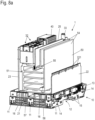
- Fig. 1 shows a first exemplary embodiment of a control system in a schematic isometric view.
- the control system includes a main module 1 and, in this example, an expansion module 2.
- the control system of the Fig. 1 is intended for installation in a control cabinet.
- the usual assembly orientation is such that the in the Fig. 1 lower, invisible, side is fixed vertically in the control cabinet.
- This page is also referred to below as the assembly page.
- the ones in the Fig. 1 The top side is therefore aligned parallel to the “mounting side” and also runs vertically when installing a control cabinet. It refers to the operator or user and is hereinafter referred to as the "front”.
- the ones in the Fig. 1 The visible side facing the viewer is aligned horizontally in a typical control cabinet assembly and is hereinafter referred to as the “bottom side”.
- the ones in the Fig. 1 The invisible side facing away from the viewer, which is also aligned horizontally during control cabinet assembly, is referred to as the “top side”.
- the expansion module 2 On the left side of the main module 1 is the expansion module 2, which is shown in the figure for better illustration Fig. 1 is shown separately from main module 1. This left side of the main module 1 or the expansion module 2 is also the left side when installed in the control cabinet and is referred to as such below.
- the main module 1 has a base 10 on which a housing cover 60 is placed.
- the base 10 is preferably constructed from several components, in the present case from three locking supports 11 aligned parallel to one another, which are spaced apart from one another by spacer elements 16.
- the locking supports 11 are used to attach the main module 1 to a top-hat rail of the control cabinet, onto which they can be snapped.
- unlocking levers 13 are arranged on each locking support 11, which unlock the locking supports 11 when actuated, so that the main module 1 can be removed from the top-hat rail.
- the latching support 11 arranged on the right side of the main module 1 has protruding latching hooks 14 with which the input/output modules 3 mentioned can be latched to the main module 1.
- the input/output modules 3 are equipped with comparable locking supports 11 so that they can be placed on the top-hat rail and snapped onto the main module 1 by pushing them towards them.
- the right locking carrier 11 of the main module 1 also carries various bus contacts 15, via which a power supply and data can be transmitted to the attached input/output modules 3.
- the mechanical design of the right side of the main module 1 as well as the electrical and mechanical design of the bus contacts 15 corresponds to that of a fieldbus coupler with the same system, so that the input / output modules 3 designed for this fieldbus coupler with the same system can be connected directly to the main module 1 of the control system. This enables the input/output modules 3 to be used directly without an intermediate fieldbus and fieldbus coupler.
- the right side of the main module 1 is designed in the same form factor as the input/output modules 3. It has a section in which power supply connections 31 are positioned.
- the power supply connections 31 are designed as plug-in elements with a circuit board end connector, which is located on a printed circuit board underneath (see e.g Fig. 2a or 3a ) can be attached.
- the plug-in elements can provide various desired types of contact as power supply connections 31, for example push-in contacts, screw contacts or plug connectors.
- the housing cover 60 is designed in this area as a fold-up strip 62. This system and this form factor is preferably implemented in a comparable manner in the attachable input/output modules 3.
- the installation space of the main module 1 is larger and the housing cover 60 is formed by a main cover 61 which projects higher than the folding strip 62.
- Ventilation openings 63 are preferably formed on the bottom and top, through which a convection air flow passes from bottom to top through the main module 1.
- a fan can be placed on the bottom or top of the main cover 61, which causes a forced air flow through the main module 1 for better cooling.
- filter elements can also be provided which minimize the penetration of dirt through the ventilation openings 63.
- connections 30 are provided on the underside, whereas the front of the main module 1 has switching and signaling elements 40, for example status displays, switches or buttons.
- An antenna connection 33 is also arranged on the front.
- a memory card connection 34 with an insertion slot for, for example, a (micro) SD memory card is arranged on the front. Details about the internal structure of the main module 1 are explained in the following figures.
- the expansion module 2 which can be plugged into the left side of the main module 1, has a fundamentally comparable structure.
- the expansion module 2 also includes a base 10' which has locking supports 11' which are spaced apart from one another by spacer elements 16'. Latching hooks 14' serve for a latching connection to the main module 1.
- a housing cover 60' of the expansion module 2 is only indicated by dashed outlines and is otherwise shown transparently, so that an internal structure is visible.
- a circuit board 20 ' is arranged vertically, which is in the Fig. 1 top end carries connections 30'. These are accessible from the front of the expansion module 2.
- the structure of the expansion module 2 is also shown in more detail in the following figures.
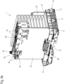
- FIG. 2a to 2c Another exemplary embodiment of a control system is shown in various views.
- the Fig. 2a and 2 B each show a schematic isometric view from two different viewing directions and the Fig. 2c shows a top view of the front of the control system.
- Housing covers 60, 60' are removed to provide insight into the internal structure of the control system.
- a main module 1 is connected to two expansion modules 2. Both expansion modules 2 are plugged in one behind the other on the left side of the main module 1, so a first expansion module 2 is directly connected to the main module 1 and a second expansion module 2 is plugged into the first expansion module 2. This is possible because the bus contacts 15 'of the expansion module 2 are looped through, so that several expansion modules 2 can be arranged in a row. For this purpose, the left side of each expansion module 2 is designed analogously to the left side of the main module 1.
- the main module 1 and the expansion modules 2 shown are constructed in a comparable manner to the first exemplary embodiment Fig. 1 .
- Small differences relate to the design of the heat sink 50, which is the case in the exemplary embodiment Fig. 2a to 2c takes up the entire height of the main module 1, whereas in the exemplary embodiment the Fig. 1 a free space remains above the heat sink 50, which can possibly be used for other purposes.
- bus contacts 15 ' which is the case in the exemplary embodiment Fig. 2a to 2c are not designed as circuit board edge connectors. Instead, plug connectors 26 and 26' are provided, which are plugged into one another and have bus contacts 15'.
- the expansion modules have the Fig. 2a to 2c also has a circuit board 20' aligned parallel to the mounting side or front side, which accommodates the plug connectors for the bus contacts 15' and which are electrically connected to another plug connector with main (circuit boards) 20' aligned perpendicular to it.
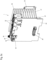
- FIG. 3a , 3b and 4a - 4c an exemplary embodiment of a main module 1 of a controller is shown in more detail.
- the Fig. 3a and 3b show the main module 1 without the housing cover 60 attached in order to gain an insight into the internal structure.
- the 4a to 4c show different views of the main module 1 with the housing cover 60 attached.
- the Fig 3a , 4b and 4a , 4b are isometric views from different viewing directions and the Fig .4c a top view of the front of the main module 1.
- the design of the base 10 of the main module 1 corresponds to that of the main modules 1 according to Fig. 1 and 2a until 2c . Reference is hereby made to the associated description.
- the present main module 1 has a plurality of circuit boards 20, the arrangement and function of which are explained in more detail below.
- a backplane bus circuit board 21 is initially arranged, which extends over the entire surface of the base frame 18. Towards the right side, the backplane bus circuit board 21 extends slightly beyond the base frame 18 to the circuit board support 17.
- the circuit board carrier 17 carries vertically a connection circuit board 22, which is inserted into the circuit board carrier 17 and extends to the bus contacts 15 on the right side of the main module 1.
- connection circuit board 22 is perpendicular to the backplane bus circuit board 21 and is connected to it via an angled plug connector 26.
- the connection circuit board 22 has at its upper end circuit board edge connectors, onto which the power supply connections 31, which are arranged in the folding strip 62 (cf. 4a to 4c ) are attached.
- the main module 1 is supplied with supply voltage, usually a direct voltage in the range of 24V, via these power supply connections 31.
- Electronic components for providing the power supply to the main module 1 and the input/output modules 3 as well as plugged-in expansion modules 2 are arranged on the connection circuit board 22.
- components arranged on circuit boards 20 are only shown as examples. It is understood that the space on all circuit boards 20 not occupied by components shown in the figures is available for electrical or electronic components. All circuit boards 20 can be populated on one or (preferably) on both sides.
- the backplane bus circuit board 21 accommodates a backplane bus for the main module 1 and any expansion modules 2.
- the backplane bus provides power supply and data lines.
- the data lines form at least one standardized and/or proprietary data bus.
- the lines of the backplane bus are passed on, for example, via the bus contacts 15 'to an inserted expansion module 2.
- main circuit board 23 vertically approximately in the middle of the main module 1, which accommodates the essential functional elements of the main module 1, in particular one or more CPU (Central Processing Unit), one or more FPGA (Field Programmable Gate Array), memory components such as RAM ( Random Access Memory), NVRAM (Non Volatile RAM), an RTC (Real Time Clock), as well as interface drivers for interface connections 32 and switching and signal elements 40.
- CPU Central Processing Unit
- FPGA Field Programmable Gate Array
- RAM Random Access Memory
- NVRAM Non Volatile RAM
- RTC Real Time Clock
- interface connections 32 and switching and signal elements 40 are arranged in the front (upper in the figures) area of the main circuit board 23.
- the switching and signal elements 40 as well as the antenna connection 33 can be arranged on the edge of the main circuit board 23, whereas the various interface connections 32 are positioned on the side of the main circuit board 23 facing away from the connection circuit board 22.
- 32 RJ-45 connections are provided as interface connections or D-SUB connections, which are also used as fieldbus connections.
- interface connections 32 can be designed as SFP (Small Formfactor Plugable) network connections, as USB connections, as display connections or even as BL/SL connections.
- the antenna connection 33 can be designed, for example, as an SMA high-frequency connection.
- a heat sink 50 is positioned between the connection circuit board 22 and the main circuit board 23.
- a cooling surface 51 facing the main circuit board 23 is in thermal contact with heat-generating components of the main circuit board 23, which are preferably arranged on the side of the circuit board facing the heat sink 50. All heat-generating components such as the CPU, the FPGAs, etc. can be cooled via the heat sink 50.
- the heat sink 50 is attached to mounting domes 19, which are formed in the base 10.
- the mounting domes 19 can be guided through an opening in the backplane bus circuit board 21, so that the heat sink is connected directly to the base 10.
- the mounting domes 19 can end below the backplane bus circuit board 21 and a screw can be inserted through the backplane bus circuit board 21 and a spacer into the Heat sink 50 guide so that the heat sink 50 is attached to the base 10 together with the backplane bus circuit board 21.
- the upper cooling channel 52 in the figures which faces the front side, is not formed over the entire width of the heat sink 50, so that a free space is created on the back of the main circuit board 23 in which a small additional circuit board 25 aligned parallel to the main circuit board 23 is positioned.
- This can be connected to the main circuit board 23 via soldering pins and/or plug connectors and can accommodate additional switching and signaling elements 40 or connections 30.
- the additional circuit board 25 provides a memory card connection 34 for accommodating a micro SD memory card and a battery connection 3 for accommodating and contacting a buffer battery to supply z.
- RTC real time clock
- the area in which the memory card connection 34 and also the battery is arranged can be covered by an access flap 64 in order to protect an inserted memory card or battery from being accidentally removed.
- a display can also be arranged in the main cover 61, or an opening through which a display is accessible. The display can be equipped with a touch function and form a switching and signaling element 40.
- the interface connections 32 positioned in the front in this exemplary embodiment can also be accessible from the underside of the main module 1 in alternative configurations, as is the case in the exemplary embodiment Fig. 1 and 2a until 2c is implemented.
- an optional additional circuit board 24 is arranged parallel to the main circuit board 23.
- This additional circuit board 24 can, for example, also have interface drivers and further interface connections 32, which are then accessible on the front or bottom of the main module 1. In this way, a larger variety of interfaces can be provided.
- the individual interface connections 32 are positioned on the main circuit board 23 and the additional circuit board 24 in such a way that they utilize the installation space between these circuit boards without interfering with each other.
- the supplementary circuit board 24 can also be used to provide particularly fast input/output channels via FPGA or GPIO (General Purpose Input Output) modules with, if necessary, direct access to the backplane bus. In this way, special input/output channels with switching times in the nanosecond range can be implemented.
- FPGA Field Programmable Gate array
- GPIO General Purpose Input Output
- the plug contact is mounted in a recess in the expansion circuit board 25 on the backplane bus circuit board 21 in order to connect expansion modules 2 to the main module 1 via its bus contacts 15 '.
- the backplane bus circuit board 21 can alternatively also be used to accommodate backup capacitors for smoothing and supporting the power supply line of the backplane bus. It is also conceivable to arrange the buffer battery of the real-time clock (RTC), which is located on the additional circuit board 25 in the exemplary embodiment shown, on the backplane bus circuit board 21. A flap or cover is then provided at the appropriate location in the housing cover 60 through which the backup battery is accessible and can be replaced.
- RTC real-time clock
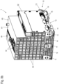
- FIG. 5a to 5d and 6a to 6c A further exemplary embodiment of a main module 1 of a control system is shown.
- the Fig. 5a to 5d show the main module 1 without the housing cover 60 attached, whereas the Fig. 6a to 6c the main module 1 with the housing cover 60 attached.
- the base 10 of the main module 1 is designed as in the previous exemplary embodiments, to which reference is hereby made. The differences from the previously described exemplary embodiments are essentially discussed below.
- connection circuit board 22 and the backplane bus circuit board 21 and any additional circuit boards 25 used only a main circuit board 23 and no additional circuit board 24 are provided.
- the main circuit board 23 is arranged in the area of the left side of the main module 1.
- the switching and signaling elements 40 are in turn positioned along a portion of the upper (as shown in the figures) edge of the main circuit board 23. Due to the arrangement of the main circuit board 23 on the side in the main module 1, the interface connections 32 (again in particular RJ-45 and USB ports) which clearly protrude from the main circuit board 23 are arranged to the right in the main module 1 on the main circuit board 23.
- the heat sink 50 is brought close to the main circuit board 23 in order to be able to thermally connect heat-emitting components of the main circuit board to the heat sink 50 and to be able to cool them via the heat sink 50.
- the heat sink 50 In the upper area of the heat sink 50 it is notched out in order to be able to provide space for the interface connections 32 and the additional circuit board 25. If the cooling requirement is lower, you may be able to use the one next to the interface connections 32 located section of the heat sink 50 can be omitted, so that in turn more space for the additional circuit board 25 or space for an additional circuit board 25 aligned parallel to the front side is provided.
- Another difference from the previous exemplary embodiments relates to the design of the circuit boards 20 in the area of the connection between the backplane bus circuit board 21 and the main circuit board 23.
- the backplane bus circuit board 21 in turn opens into a plug-in contact, via which the backplane bus can be transferred to plug-in expansion modules 2.
- the backplane bus circuit board 21 is only guided in the area of this plug contact up to the edge of the base frame 18 of the main module 1.
- the backplane bus circuit board 21 ends in front of the main circuit board 23. This allows the main circuit board 23 to be extended downwards into the base 10, which means more assembly space is available. The area of the connector to the expansion modules 2 is left out.
- FIG. 5c is the main module 1 from the same viewing direction as at Fig. 5b reproduced, but the base 10 is removed in order to be able to display the main circuit board 23 in its entire size.
- This figure also shows that the heat sink 50 with a section that forms a mounting foot 57 also protrudes into the base 10, which serves to fasten it.
- an angle connector (not shown here) is arranged, which transfers the backplane bus from the main circuit board 23 to the backplane bus circuit board 21.
- both connectors can be combined in such a way that the main circuit board 23 has a connector on the front and back, which on the one hand interacts with a corresponding mating connector on the backplane bus circuit board 21 and forwards the backplane bus to the expansion module 2.
- Such an arrangement of connectors is also referred to as a 180° connector.
- the larger area of the main circuit board 23 that can be achieved in this way makes it possible to accommodate the essential functions on one circuit board, whereby the additional circuit board 24 can be omitted. For most required applications, sufficient circuit board area is provided with compact housing dimensions.
- the variant shown in these figures therefore represents a cost-effective version of the control system.
- the formation of all essential components on the main circuit board 23 also offers the advantage that that high-frequency clocked signals are routed via a few connectors, which results in good signal flow and thus the use of high clock frequencies. Saving the additional circuit board 24 also has a cost-reducing effect on the system.
- the antenna connection 33 is arranged on the additional circuit board 25. This is advantageous if the antenna connection 33 is not part of the basic equipment of the main module 1, but can be added later by retrofitting the additional circuit board 25.
- the memory card connection 34 is also formed on the main circuit board 23. All connections and function blocks necessary to operate the main module can be implemented on the main circuit board 23 or the backplane bus circuit board 21 and the connection circuit board 22. Optional features such as the antenna connection 33 can then be retrofitted via the additional circuit board. As already mentioned in connection with the previous exemplary embodiment, a backup battery for a real-time clock of the system can be located, for example, on the backplane bus circuit board 21.
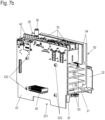
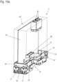
- FIG. 7a to e and 8a and 8b a further exemplary embodiment of a main module 1 of a controller is shown in different views.
- the Fig. 7a to e show the main module 1 without the housing.
- Fig. 8a is the one in the Fig. 7a
- the arrangement shown to e is inserted into a base 10.
- Fig. 8b Finally, the complete main module 1 with base 10 and attached upper housing part 60 is shown.
- the Fig. 7a and 7b are isometric oblique views of main module 1, which is shown here without base 10 and without attached housing cover 60
- Fig. 7c shows a top view of the main module 1, which Fig. 7d a side view and the Fig. 7e a top view of the underside of the main module 1, i.e. a view from the direction of the base 10, not shown here.
- Fig. 7a to e and 8a, b are constructed in the same way as the main modules 1 described in connection with the previous figures.
- a plurality of circuit boards 20 are present, specifically a backplane bus circuit board 21, a connection circuit board 22, a main circuit board 23 and an additional circuit board 25.
- the backplane bus circuit board 21 lies parallel to a top-hat rail onto which the main module 1 can be snapped.
- the backplane bus circuit board 21 is also located like this Fig. 8a shows, on base 10 on, which in turn has 3 locking supports 11, which are spaced apart from one another by spacer elements 16.
- the main circuit board 23, the connection circuit board 22 and the additional circuit board 25 are arranged vertically.
- the heat sink 50 is arranged centrally in the main module 1 and, in addition to its function for cooling components of the main module 1, also serves to hold several of the circuit boards 20.
- the heat sink 50 thus represents the central and supporting element of the main module 1 .It extends over the entire extent of the main module 1 in a direction perpendicular to the top-hat rail, i.e. H. in the direction in which the locking supports 11 also run.
- the cooling channels 52 are also formed by inner fins 53.
- the cooling channels 52 run vertically, so that a draft of cooling air begins through the cooling channels 52 due to convection.
- a fan can be placed on the outside of the housing 60, which increases a draft through the ventilation openings 63 and the cooling channels 52.
- the inner cooling fins 53 are formed parallel to the rear wall of the circuit board 21. They thus dissipate heat from the cooling surface 51, which runs parallel to the main circuit board 23.
- the inner fins 53 do not extend to the opposite wall of the heat sink 50 in order to simplify its production in a continuous die-casting process.
- the cooling surface 51 can be designed to be stepped and have plateaus at different heights in order to contact components of the main circuit board of different heights equally well.
- the otherwise cuboid outline of the heat sink 50 is recessed in order to provide space for the interface connections 32 and / or switching and signaling elements 40, which are arranged on the main circuit board 23.
- outer cooling fins 54 are aligned parallel to the main circuit board 23. They are therefore also parallel to the additional circuit board 25, which, for example, accommodates modules for wireless communication and carries an antenna connection 33. Elements to be cooled on the additional circuit board 25 can be connected to the neighboring one Cooling fin 54 may be coupled.
- a fastening groove 55 is provided in the heat sink 50, which serves to fasten the circuit board 25.
- the main circuit board 23 is mounted on the heat sink 50.
- Fastening screws 232 can be seen, which lead through the main circuit board 23 and are screwed into corresponding threaded holes in the heat sink 50.
- the backplane bus circuit board 21 is also screwed to the heat sink 50, which has fastening holes 56 for this purpose, for example in Fig. 7a can be recognized.
- the backplane bus circuit board 21 and the main circuit board 23, as well as the additional circuit board 25, together with the heat sink 50 form a pre-assembled assembly which is electrically functional in itself and which is inserted as a whole into the base 10 for assembly.
- the heat sink 50 is comparable to the exemplary embodiment Fig. 5a-d or 6a-c mounting feet 57, with which it protrudes through a recess on the edge of the backplane bus circuit board 21 into the area of the base 10.
- Guides for the mounting feet 57 are preferably formed in the base 10, which accommodate an inserted heat sink 50 in a form-fitting manner on the side.
- the main circuit board 23 is also continued downwards beyond the level of the backplane bus circuit board 21 in the direction of the base 10 and, like the mounting feet 57, protrudes into the base 10. In this way, additional assembly space is created on the main circuit board 23 without increasing the overall height of the main module 1, ie the height above the top-hat rail.
- FIG. 7e shows the downward mounting feet 57, each with a mounting hole 58, by means of which the inserted heat sink 50 can be screwed to the base from below.
- components 211 of the backplane bus circuit board 21 can also be seen, which also protrude downwards into the base 10 and thus use its volume.
- the illustration also shows fastening screws 212 with which the backplane bus circuit board 21 is screwed to the heat sink 50.
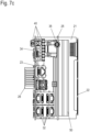
- FIG. 9 A further exemplary embodiment of a main module 1 of a controller is shown. Comparable to Fig. 8a is an isometric oblique view of the Main module 1 is shown, with a base 10 and an attached housing cover 60 not being shown in this figure.
- the basic structure corresponds to: Fig. 9 illustrated embodiment of the Figs. 7a-7e and 8a, b, particularly when it comes to assembling the heat sink 50.
- Fig. 9 illustrated embodiment of the Figs. 7a-7e and 8a, b, particularly when it comes to assembling the heat sink 50.
- it has mounting feet 57 which project downward into the base 10.
- the main board 23 and also the backplane bus board 21 are connected to the heat sink 50, for example via the ones in the Fig. 9 visible fastening screws 212.
- inner cooling fins 53 are formed parallel to the backplane bus circuit board 21 and in the upper part of the heat sink 50, which is remote from the backplane bus circuit board 21, outer cooling fins 54 are aligned perpendicular to the backplane bus circuit board 21 .
- the heat sink 50 is wider in the direction of the top-hat rail.
- a total of four outer cooling fins 54 are present parallel to the main circuit board 23 and are distributed over the entire width of the heat sink 50.
- connection made between the main circuit board 23 and the additional circuit boards 25 or between various of the additional circuit boards 25 can be connectors of various types.
- cable connectors can also be provided, particularly for transmitting high-frequency signals.
- the one in the Fig. 9 right additional board 25 a number of antenna connections 33, which are designed according to the SMA (Sub-Miniature-A) standard.
- Electronic components serving these antenna connections 33 can also be installed, for example, on the adjacent additional board also carries antenna connections 33, with high-frequency signals being exchanged between the two additional boards via miniature high-frequency plugs.
- Suitable miniature high-frequency connectors are, for example, UMTC (Ultra Miniature Telecommunications Connector) connectors.
- FIG. 9 Another difference between the exemplary embodiment Fig. 9 compared to what was previously described lies in the presence of an additional circuit board 24, which supplements the functionality of the main circuit board 23.
- This is arranged parallel to the main circuit board 23 and is connected to it via a circuit board connector which is formed in the plane of the backplane bus circuit board 21.
- memory modules 241 are arranged on the sides of the supplementary circuit board 24 opposite the main circuit board 23. The memory modules 241 are therefore accessible after removing the housing cover 60, not shown here, in order to be able to be supplemented or replaced.
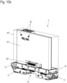
- FIG. 10a and 10b and 11a and 11b each show isometric views from different directions of two examples of an expansion module 2 for a control system.
- the first, in the Fig. 10a and 10b The example shown is also in the control system Fig. 1 shown.
- the second, in the Fig. 11a and 11b The example of the expansion module 2 shown is shown in the example Fig. 2a to 2c used.
- FIG. 10a and 10b A vertically arranged main circuit board 23' is provided, which has connections 30', specifically interface connections 32', on its upper edge (in the figures), i.e. facing the front.
- a so-called 180° plug connector is arranged, which provides plug contacts on both sides of the main circuit board 23'.
- a backplane bus circuit board 21' is inserted on the right side, which extends to a cutout in the housing cover 60', which is shown as translucent in the figure.
- this backplane bus circuit board 21' contacts a corresponding connector in the main module 1.
- a similar connector is provided on the left side of the expansion module 2 for contacting further expansion modules 2.
- a backplane bus circuit board 21 ' is provided, which is aligned parallel to the mounting side or front side and which has a connector on each of the sides of the expansion module 2.
- the main circuit board 23' is placed vertically on the backplane bus circuit board 21' and is electrically connected to it via another plug connector.
- a section of the main circuit board 23 ' protrudes into the base 10, whereby, for example, ground contact can be made via a contact spring arranged in the base 10 to the top-hat rail.
- the expansion modules 2 expand the control system with additional interfaces or application modules.
- Application modules can contain functions or combinations of interfaces. Application modules combine functions for specific application areas.
- the direct connection of the expansion modules 2 to the backplane bus of the main module 1 makes it possible to exchange a high data rate via the expansion modules 2.
- the expansion modules 2 can also be viewed as “high-speed modules” or can form an output module for particularly short switching times.
- the expansion modules 2 can also be used as memory modules, as repeaters, as camera modules, as gateways, as multiplayer or as switches, as media converters, as routers for data analysis (e.g. predictive analytics) or for providing security functions ( Safety).
- the Fig. 12a to 12c each show a schematic top view of the front (only in the area of the main cover 61) of the main module 1.
- FIG. 12a to 12c Various possible constellations of the front with connections 30 and switching and signaling elements 40 are shown schematically and not in the exact geometric position.
- the different designs of the Fig. 12a to 12c differ in the type of connections 30 or switching and signaling elements 40 and in particular the density with which these connections 30 and switching and signaling elements 40 are arranged on the front.
- the ones in the 12a and 12b can be achieved, for example, with the basic structure of all previously shown exemplary embodiments of a main module 1.
- Fig. 12c The configuration shown with a very high density of connections 30 and switching and signaling elements 40 is preferred with the exemplary embodiments Fig. 3a and 3b and 4a to 4c and 9 can be implemented, since in these exemplary embodiments, in addition to the main circuit board 23, the additional circuit board 24 is available, in particular to accommodate additional interface connections 32.
Landscapes
- Engineering & Computer Science (AREA)
- Microelectronics & Electronic Packaging (AREA)
- Physics & Mathematics (AREA)
- Thermal Sciences (AREA)
- Cooling Or The Like Of Electrical Apparatus (AREA)
Claims (14)
- Unité de commande pour un système d'automatismes industriel, comportant un module principal (1) avec un boîtier qui comprend une embase (10) avec laquelle il peut être posé sur un rail oméga et avec au moins deux cartes de circuits (20) disposées dans le boîtier, dont l'une est une carte de circuits de bus de fond de panier (21) et une autre une carte de circuits principale (23), la carte de circuits principale (23) étant associée à un radiateur (50) pour le refroidissement de composants et la carte de circuits de bus de fond de panier (21) fournissant un bus de fond de panier pour au moins un module d'extension (2) qui peut être monté en série sur le côté, caractérisée en ce que le radiateur (50) est disposé dans le boîtier, fixé à l'embase (10), et porte au moins une des cartes de circuits (20).
- Unité de commande selon la revendication 1, dans laquelle le radiateur (50) présente un contour sensiblement quadrangulaire et deux de ses surfaces extérieures perpendiculaires l'une à l'autre sont parallèles à la carte de circuits principale (23) et à la carte de circuits de bus de fond de panier (21).
- Unité de commande selon la revendication 1 ou 2, dans laquelle au moins une surface extérieure du radiateur (50) est conformée comme une surface de refroidissement (51) avec laquelle les composants de la carte de circuits principale (23) sont en contact thermique.
- Unité de commande selon l'une des revendications 1 à 3, dans laquelle la carte de circuits de bus de fond de panier (21) est disposée à plat ou sur l'embase, de façon à être orientée parallèlement à un rail oméga sur lequel le module principal (1) est posé.
- Unité de commande selon l'une des revendications 1 à 4, dans laquelle la carte de circuits principale (23) et la carte de circuits de bus de fond de panier (21) sont fixées sur le radiateur (50).
- Unité de commande selon les revendications 4 et 5, dans laquelle le radiateur (50) comporte au moins un pied de montage (57) qui dépasse jusque dans l'embase (10) et y est fixé.
- Unité de commande selon la revendication 6, dans laquelle le radiateur (50), la carte de circuits principale (23) et la carte de circuits de bus de fond de panier (21) forment un groupe préassemblé qui est fixé ensemble sur l'embase (10).
- Unité de commande selon la revendication 7, dans laquelle le groupe n'est fixé sur l'embase (10) qu'avec l'au moins un pied de montage (57).
- Unité de commande selon l'une des revendications 1 à 8, dans laquelle le radiateur (50) comporte des ailettes de refroidissement internes (53) qui forment les canaux de refroidissement (52).
- Unité de commande selon la revendication 9, dans laquelle les ailettes de refroidissement internes (53) sont perpendiculaires à la carte de circuits principale (23).
- Unité de commande selon l'une des revendications 1 à 10, dans laquelle le radiateur (50) présente des ailettes de refroidissement externes (54) à côté desquelles au moins une carte de circuits supplémentaire (25) est disposée.
- Unité de commande selon la revendication 11, dans laquelle les ailettes de refroidissement externes (54) sont parallèles à la carte de circuits principale (23).
- Unité de commande selon la revendication 11 ou 12, dans laquelle au moins une des ailettes de refroidissement externes (54) sont plus courtes dans le sens longitudinal que d'autres parties du radiateur (50).
- Système de commande avec une unité de commande munie d'un module principal (1) selon l'une des revendications 1 à 13, dans laquelle le module principal (1) est relié par une carte de circuits de bus de fond de panier (21) à au moins un module d'extension (2) monté en série.
Applications Claiming Priority (2)
| Application Number | Priority Date | Filing Date | Title |
|---|---|---|---|
| DE202017103994 | 2017-07-04 | ||
| PCT/EP2018/068084 WO2019008032A1 (fr) | 2017-07-04 | 2018-07-04 | Commande et système de commande modulaire d'un système d'automatisation industriel |
Publications (2)
| Publication Number | Publication Date |
|---|---|
| EP3649838A1 EP3649838A1 (fr) | 2020-05-13 |
| EP3649838B1 true EP3649838B1 (fr) | 2024-01-10 |
Family
ID=62816577
Family Applications (1)
| Application Number | Title | Priority Date | Filing Date |
|---|---|---|---|
| EP18737256.0A Active EP3649838B1 (fr) | 2017-07-04 | 2018-07-04 | Commande et système de commande modulaire d'un système d'automatisation industriel |
Country Status (2)
| Country | Link |
|---|---|
| EP (1) | EP3649838B1 (fr) |
| WO (1) | WO2019008032A1 (fr) |
Families Citing this family (7)
| Publication number | Priority date | Publication date | Assignee | Title |
|---|---|---|---|---|
| DE202019100078U1 (de) | 2019-01-09 | 2020-04-15 | Weidmüller Interface GmbH & Co. KG | Steuerung und modulares Steuerungssystem eines industriellen Automatisierungssystems |
| DE102019135089A1 (de) | 2019-12-19 | 2021-06-24 | Phoenix Contact Gmbh & Co. Kg | Vorrichtung zum Signalaustausch zwischen Steuerung und Feldgeräten |
| DE202020106644U1 (de) | 2020-11-19 | 2022-02-24 | Weidmüller Interface GmbH & Co. KG | Funktionsmodul zur Steuerung und/oder Überwachung technischer Prozesse |
| CN113163658B (zh) * | 2021-03-30 | 2022-10-28 | 西南电子技术研究所(中国电子科技集团公司第十研究所) | 飞行器载综合化电子设备组织架构 |
| CN114501180B (zh) * | 2022-01-19 | 2024-06-11 | 青岛乾程科技股份有限公司 | 一种多功能模组集中器 |
| TWI839174B (zh) * | 2023-03-31 | 2024-04-11 | 台達電子工業股份有限公司 | 並聯式模組驅動器 |
| CN118739786A (zh) | 2023-03-31 | 2024-10-01 | 台达电子工业股份有限公司 | 并联式模块驱动器 |
Citations (3)
| Publication number | Priority date | Publication date | Assignee | Title |
|---|---|---|---|---|
| EP1552983A1 (fr) * | 2004-01-07 | 2005-07-13 | Goodrich Hella Aerospace Lighting Systems GmbH | Lampe, notamment avertisseur lumineux, pour véhicule |
| WO2009120942A2 (fr) * | 2008-03-28 | 2009-10-01 | Numatics, Incorporated | Système de bus électrique modulaire avec circuit incorporé de mise à la masse |
| DE102012103217B3 (de) * | 2012-04-13 | 2013-08-22 | Elka-Elektronik Gmbh | Steuerungsgerät für ein Gebäudeinstallationssystem |
Family Cites Families (5)
| Publication number | Priority date | Publication date | Assignee | Title |
|---|---|---|---|---|
| US5598322A (en) * | 1994-09-27 | 1997-01-28 | Watlow Winona, Inc. | Power control system |
| DE102006046194A1 (de) * | 2006-09-29 | 2008-04-03 | Siemens Ag | Kühlkörper zur Kühlung eines elektrischen Bauelementes |
| DE102014118389A1 (de) | 2014-12-11 | 2016-06-16 | Weidmüller Interface GmbH & Co. KG | Automatisierungsgerät, Anschlussmodul für ein Automatisierungsgerät und Verfahren zum Betreiben eines Automatisierungsgeräts |
| DE102015104290A1 (de) * | 2015-03-23 | 2016-09-29 | Phoenix Contact Gmbh & Co. Kg | Modulares Bussystem |
| DE102015111204B4 (de) * | 2015-07-10 | 2019-03-07 | Semikron Elektronik Gmbh & Co. Kg | Leistungselektronisches Modul mit Lastanschlusselementen |
-
2018
- 2018-07-04 WO PCT/EP2018/068084 patent/WO2019008032A1/fr not_active Ceased
- 2018-07-04 EP EP18737256.0A patent/EP3649838B1/fr active Active
Patent Citations (3)
| Publication number | Priority date | Publication date | Assignee | Title |
|---|---|---|---|---|
| EP1552983A1 (fr) * | 2004-01-07 | 2005-07-13 | Goodrich Hella Aerospace Lighting Systems GmbH | Lampe, notamment avertisseur lumineux, pour véhicule |
| WO2009120942A2 (fr) * | 2008-03-28 | 2009-10-01 | Numatics, Incorporated | Système de bus électrique modulaire avec circuit incorporé de mise à la masse |
| DE102012103217B3 (de) * | 2012-04-13 | 2013-08-22 | Elka-Elektronik Gmbh | Steuerungsgerät für ein Gebäudeinstallationssystem |
Also Published As
| Publication number | Publication date |
|---|---|
| WO2019008032A1 (fr) | 2019-01-10 |
| EP3649838A1 (fr) | 2020-05-13 |
Similar Documents
| Publication | Publication Date | Title |
|---|---|---|
| EP3649838B1 (fr) | Commande et système de commande modulaire d'un système d'automatisation industriel | |
| EP3909406A1 (fr) | Commande et système de commande modulaire d'un système d'automatisation industriel | |
| DE69122878T2 (de) | Erweiterungsfähige gekühlte gehäuse für computer-leiterplatten | |
| EP2946644B1 (fr) | Ensemble doté d'un module et d'un dispositif électronique | |
| EP2068228B1 (fr) | Système de traitement des données | |
| EP3057387B1 (fr) | Unite de communication, en particulier passerelle smartmeter | |
| EP1815728B1 (fr) | Systeme d'automatisation modulaire | |
| DE202006006615U1 (de) | Elektronikgehäuse | |
| EP1579747A1 (fr) | Modules d'appareil de mesure et appareil de mesure | |
| EP3123844B1 (fr) | Module de connexion et/ou de fonction compatible avec un bus et pouvant être mis en série | |
| DE102012103217B3 (de) | Steuerungsgerät für ein Gebäudeinstallationssystem | |
| DE2851749C2 (fr) | ||
| EP4218100B1 (fr) | Module fonctionnel de commande et/ou de surveillance de processus techniques | |
| DE102005062494A1 (de) | Elektrisches/elektronisches Installationsgerät | |
| EP1705976B1 (fr) | Module d'appareil de mesure | |
| DE102014109984A1 (de) | Elektronikgeräteanordnung | |
| DE102017105408A1 (de) | Elektrisches Reiheneinbaugerät und Anordnung von elektrischen Reiheneinbaugeräten | |
| EP3430875B1 (fr) | Bloc de jonction électronique pour bus de données | |
| EP3660603B1 (fr) | Module fonctionnel pouvant être disposé en rang, adapté bus | |
| DE102021126189A1 (de) | Elektronisches Gerät mit einem Zusatzmodul | |
| EP3447847B1 (fr) | Élément de raccordement et système de raccordement permettant de raccorder une carte de circuit imprimé à un ordinateur central d'un véhicule automobile | |
| DE202020106644U1 (de) | Funktionsmodul zur Steuerung und/oder Überwachung technischer Prozesse | |
| DE4406520A1 (de) | Anordnung elektrischer Montagekomponenten einer Rechnereinheit | |
| DE3041726C2 (de) | Geräteeinsatz der Vertikalbauweise | |
| DE19931908C2 (de) | Elektronische Anlage |
Legal Events
| Date | Code | Title | Description |
|---|---|---|---|
| STAA | Information on the status of an ep patent application or granted ep patent |
Free format text: STATUS: UNKNOWN |
|
| STAA | Information on the status of an ep patent application or granted ep patent |
Free format text: STATUS: THE INTERNATIONAL PUBLICATION HAS BEEN MADE |
|
| PUAI | Public reference made under article 153(3) epc to a published international application that has entered the european phase |
Free format text: ORIGINAL CODE: 0009012 |
|
| STAA | Information on the status of an ep patent application or granted ep patent |
Free format text: STATUS: REQUEST FOR EXAMINATION WAS MADE |
|
| 17P | Request for examination filed |
Effective date: 20191122 |
|
| AK | Designated contracting states |
Kind code of ref document: A1 Designated state(s): AL AT BE BG CH CY CZ DE DK EE ES FI FR GB GR HR HU IE IS IT LI LT LU LV MC MK MT NL NO PL PT RO RS SE SI SK SM TR |
|
| AX | Request for extension of the european patent |
Extension state: BA ME |
|
| DAV | Request for validation of the european patent (deleted) | ||
| DAX | Request for extension of the european patent (deleted) | ||
| STAA | Information on the status of an ep patent application or granted ep patent |
Free format text: STATUS: EXAMINATION IS IN PROGRESS |
|
| 17Q | First examination report despatched |
Effective date: 20220103 |
|
| GRAP | Despatch of communication of intention to grant a patent |
Free format text: ORIGINAL CODE: EPIDOSNIGR1 |
|
| STAA | Information on the status of an ep patent application or granted ep patent |
Free format text: STATUS: GRANT OF PATENT IS INTENDED |
|
| INTG | Intention to grant announced |
Effective date: 20231017 |
|
| GRAS | Grant fee paid |
Free format text: ORIGINAL CODE: EPIDOSNIGR3 |
|
| GRAA | (expected) grant |
Free format text: ORIGINAL CODE: 0009210 |
|
| STAA | Information on the status of an ep patent application or granted ep patent |
Free format text: STATUS: THE PATENT HAS BEEN GRANTED |
|
| P01 | Opt-out of the competence of the unified patent court (upc) registered |
Effective date: 20231116 |
|
| AK | Designated contracting states |
Kind code of ref document: B1 Designated state(s): AL AT BE BG CH CY CZ DE DK EE ES FI FR GB GR HR HU IE IS IT LI LT LU LV MC MK MT NL NO PL PT RO RS SE SI SK SM TR |
|
| REG | Reference to a national code |
Ref country code: GB Ref legal event code: FG4D Free format text: NOT ENGLISH |
|
| REG | Reference to a national code |
Ref country code: CH Ref legal event code: EP |
|
| REG | Reference to a national code |
Ref country code: DE Ref legal event code: R096 Ref document number: 502018013954 Country of ref document: DE |
|
| REG | Reference to a national code |
Ref country code: IE Ref legal event code: FG4D Free format text: LANGUAGE OF EP DOCUMENT: GERMAN |
|
| REG | Reference to a national code |
Ref country code: LT Ref legal event code: MG9D |
|
| REG | Reference to a national code |
Ref country code: NL Ref legal event code: MP Effective date: 20240110 |
|
| PG25 | Lapsed in a contracting state [announced via postgrant information from national office to epo] |
Ref country code: NL Free format text: LAPSE BECAUSE OF FAILURE TO SUBMIT A TRANSLATION OF THE DESCRIPTION OR TO PAY THE FEE WITHIN THE PRESCRIBED TIME-LIMIT Effective date: 20240110 |
|
| PG25 | Lapsed in a contracting state [announced via postgrant information from national office to epo] |
Ref country code: NL Free format text: LAPSE BECAUSE OF FAILURE TO SUBMIT A TRANSLATION OF THE DESCRIPTION OR TO PAY THE FEE WITHIN THE PRESCRIBED TIME-LIMIT Effective date: 20240110 |
|
| PG25 | Lapsed in a contracting state [announced via postgrant information from national office to epo] |
Ref country code: IS Free format text: LAPSE BECAUSE OF FAILURE TO SUBMIT A TRANSLATION OF THE DESCRIPTION OR TO PAY THE FEE WITHIN THE PRESCRIBED TIME-LIMIT Effective date: 20240510 |
|
| PG25 | Lapsed in a contracting state [announced via postgrant information from national office to epo] |
Ref country code: LT Free format text: LAPSE BECAUSE OF FAILURE TO SUBMIT A TRANSLATION OF THE DESCRIPTION OR TO PAY THE FEE WITHIN THE PRESCRIBED TIME-LIMIT Effective date: 20240110 |
|
| PG25 | Lapsed in a contracting state [announced via postgrant information from national office to epo] |
Ref country code: GR Free format text: LAPSE BECAUSE OF FAILURE TO SUBMIT A TRANSLATION OF THE DESCRIPTION OR TO PAY THE FEE WITHIN THE PRESCRIBED TIME-LIMIT Effective date: 20240411 |
|
| PG25 | Lapsed in a contracting state [announced via postgrant information from national office to epo] |
Ref country code: RS Free format text: LAPSE BECAUSE OF FAILURE TO SUBMIT A TRANSLATION OF THE DESCRIPTION OR TO PAY THE FEE WITHIN THE PRESCRIBED TIME-LIMIT Effective date: 20240410 Ref country code: HR Free format text: LAPSE BECAUSE OF FAILURE TO SUBMIT A TRANSLATION OF THE DESCRIPTION OR TO PAY THE FEE WITHIN THE PRESCRIBED TIME-LIMIT Effective date: 20240110 |
|
| PG25 | Lapsed in a contracting state [announced via postgrant information from national office to epo] |
Ref country code: ES Free format text: LAPSE BECAUSE OF FAILURE TO SUBMIT A TRANSLATION OF THE DESCRIPTION OR TO PAY THE FEE WITHIN THE PRESCRIBED TIME-LIMIT Effective date: 20240110 |
|
| PG25 | Lapsed in a contracting state [announced via postgrant information from national office to epo] |
Ref country code: RS Free format text: LAPSE BECAUSE OF FAILURE TO SUBMIT A TRANSLATION OF THE DESCRIPTION OR TO PAY THE FEE WITHIN THE PRESCRIBED TIME-LIMIT Effective date: 20240410 Ref country code: NO Free format text: LAPSE BECAUSE OF FAILURE TO SUBMIT A TRANSLATION OF THE DESCRIPTION OR TO PAY THE FEE WITHIN THE PRESCRIBED TIME-LIMIT Effective date: 20240410 Ref country code: LT Free format text: LAPSE BECAUSE OF FAILURE TO SUBMIT A TRANSLATION OF THE DESCRIPTION OR TO PAY THE FEE WITHIN THE PRESCRIBED TIME-LIMIT Effective date: 20240110 Ref country code: IS Free format text: LAPSE BECAUSE OF FAILURE TO SUBMIT A TRANSLATION OF THE DESCRIPTION OR TO PAY THE FEE WITHIN THE PRESCRIBED TIME-LIMIT Effective date: 20240510 Ref country code: HR Free format text: LAPSE BECAUSE OF FAILURE TO SUBMIT A TRANSLATION OF THE DESCRIPTION OR TO PAY THE FEE WITHIN THE PRESCRIBED TIME-LIMIT Effective date: 20240110 Ref country code: GR Free format text: LAPSE BECAUSE OF FAILURE TO SUBMIT A TRANSLATION OF THE DESCRIPTION OR TO PAY THE FEE WITHIN THE PRESCRIBED TIME-LIMIT Effective date: 20240411 Ref country code: ES Free format text: LAPSE BECAUSE OF FAILURE TO SUBMIT A TRANSLATION OF THE DESCRIPTION OR TO PAY THE FEE WITHIN THE PRESCRIBED TIME-LIMIT Effective date: 20240110 Ref country code: BG Free format text: LAPSE BECAUSE OF FAILURE TO SUBMIT A TRANSLATION OF THE DESCRIPTION OR TO PAY THE FEE WITHIN THE PRESCRIBED TIME-LIMIT Effective date: 20240110 |
|
| PG25 | Lapsed in a contracting state [announced via postgrant information from national office to epo] |
Ref country code: PL Free format text: LAPSE BECAUSE OF FAILURE TO SUBMIT A TRANSLATION OF THE DESCRIPTION OR TO PAY THE FEE WITHIN THE PRESCRIBED TIME-LIMIT Effective date: 20240110 Ref country code: PT Free format text: LAPSE BECAUSE OF FAILURE TO SUBMIT A TRANSLATION OF THE DESCRIPTION OR TO PAY THE FEE WITHIN THE PRESCRIBED TIME-LIMIT Effective date: 20240510 |
|
| PG25 | Lapsed in a contracting state [announced via postgrant information from national office to epo] |
Ref country code: SE Free format text: LAPSE BECAUSE OF FAILURE TO SUBMIT A TRANSLATION OF THE DESCRIPTION OR TO PAY THE FEE WITHIN THE PRESCRIBED TIME-LIMIT Effective date: 20240110 Ref country code: PT Free format text: LAPSE BECAUSE OF FAILURE TO SUBMIT A TRANSLATION OF THE DESCRIPTION OR TO PAY THE FEE WITHIN THE PRESCRIBED TIME-LIMIT Effective date: 20240510 Ref country code: PL Free format text: LAPSE BECAUSE OF FAILURE TO SUBMIT A TRANSLATION OF THE DESCRIPTION OR TO PAY THE FEE WITHIN THE PRESCRIBED TIME-LIMIT Effective date: 20240110 Ref country code: LV Free format text: LAPSE BECAUSE OF FAILURE TO SUBMIT A TRANSLATION OF THE DESCRIPTION OR TO PAY THE FEE WITHIN THE PRESCRIBED TIME-LIMIT Effective date: 20240110 |
|
| PG25 | Lapsed in a contracting state [announced via postgrant information from national office to epo] |
Ref country code: DK Free format text: LAPSE BECAUSE OF FAILURE TO SUBMIT A TRANSLATION OF THE DESCRIPTION OR TO PAY THE FEE WITHIN THE PRESCRIBED TIME-LIMIT Effective date: 20240110 |
|
| REG | Reference to a national code |
Ref country code: DE Ref legal event code: R097 Ref document number: 502018013954 Country of ref document: DE |
|
| PG25 | Lapsed in a contracting state [announced via postgrant information from national office to epo] |
Ref country code: SM Free format text: LAPSE BECAUSE OF FAILURE TO SUBMIT A TRANSLATION OF THE DESCRIPTION OR TO PAY THE FEE WITHIN THE PRESCRIBED TIME-LIMIT Effective date: 20240110 |
|
| PG25 | Lapsed in a contracting state [announced via postgrant information from national office to epo] |
Ref country code: EE Free format text: LAPSE BECAUSE OF FAILURE TO SUBMIT A TRANSLATION OF THE DESCRIPTION OR TO PAY THE FEE WITHIN THE PRESCRIBED TIME-LIMIT Effective date: 20240110 Ref country code: CZ Free format text: LAPSE BECAUSE OF FAILURE TO SUBMIT A TRANSLATION OF THE DESCRIPTION OR TO PAY THE FEE WITHIN THE PRESCRIBED TIME-LIMIT Effective date: 20240110 |
|
| PG25 | Lapsed in a contracting state [announced via postgrant information from national office to epo] |
Ref country code: SK Free format text: LAPSE BECAUSE OF FAILURE TO SUBMIT A TRANSLATION OF THE DESCRIPTION OR TO PAY THE FEE WITHIN THE PRESCRIBED TIME-LIMIT Effective date: 20240110 |
|
| PG25 | Lapsed in a contracting state [announced via postgrant information from national office to epo] |
Ref country code: SM Free format text: LAPSE BECAUSE OF FAILURE TO SUBMIT A TRANSLATION OF THE DESCRIPTION OR TO PAY THE FEE WITHIN THE PRESCRIBED TIME-LIMIT Effective date: 20240110 Ref country code: SK Free format text: LAPSE BECAUSE OF FAILURE TO SUBMIT A TRANSLATION OF THE DESCRIPTION OR TO PAY THE FEE WITHIN THE PRESCRIBED TIME-LIMIT Effective date: 20240110 Ref country code: RO Free format text: LAPSE BECAUSE OF FAILURE TO SUBMIT A TRANSLATION OF THE DESCRIPTION OR TO PAY THE FEE WITHIN THE PRESCRIBED TIME-LIMIT Effective date: 20240110 Ref country code: EE Free format text: LAPSE BECAUSE OF FAILURE TO SUBMIT A TRANSLATION OF THE DESCRIPTION OR TO PAY THE FEE WITHIN THE PRESCRIBED TIME-LIMIT Effective date: 20240110 Ref country code: DK Free format text: LAPSE BECAUSE OF FAILURE TO SUBMIT A TRANSLATION OF THE DESCRIPTION OR TO PAY THE FEE WITHIN THE PRESCRIBED TIME-LIMIT Effective date: 20240110 Ref country code: CZ Free format text: LAPSE BECAUSE OF FAILURE TO SUBMIT A TRANSLATION OF THE DESCRIPTION OR TO PAY THE FEE WITHIN THE PRESCRIBED TIME-LIMIT Effective date: 20240110 |
|
| PLBE | No opposition filed within time limit |
Free format text: ORIGINAL CODE: 0009261 |
|
| STAA | Information on the status of an ep patent application or granted ep patent |
Free format text: STATUS: NO OPPOSITION FILED WITHIN TIME LIMIT |
|
| 26N | No opposition filed |
Effective date: 20241011 |
|
| PG25 | Lapsed in a contracting state [announced via postgrant information from national office to epo] |
Ref country code: MC Free format text: LAPSE BECAUSE OF FAILURE TO SUBMIT A TRANSLATION OF THE DESCRIPTION OR TO PAY THE FEE WITHIN THE PRESCRIBED TIME-LIMIT Effective date: 20240110 |
|
| PG25 | Lapsed in a contracting state [announced via postgrant information from national office to epo] |
Ref country code: LU Free format text: LAPSE BECAUSE OF NON-PAYMENT OF DUE FEES Effective date: 20240704 |
|
| GBPC | Gb: european patent ceased through non-payment of renewal fee |
Effective date: 20240704 |
|
| PG25 | Lapsed in a contracting state [announced via postgrant information from national office to epo] |
Ref country code: LU Free format text: LAPSE BECAUSE OF NON-PAYMENT OF DUE FEES Effective date: 20240704 |
|
| PG25 | Lapsed in a contracting state [announced via postgrant information from national office to epo] |
Ref country code: SI Free format text: LAPSE BECAUSE OF FAILURE TO SUBMIT A TRANSLATION OF THE DESCRIPTION OR TO PAY THE FEE WITHIN THE PRESCRIBED TIME-LIMIT Effective date: 20240110 Ref country code: BE Free format text: LAPSE BECAUSE OF NON-PAYMENT OF DUE FEES Effective date: 20240731 |
|
| PG25 | Lapsed in a contracting state [announced via postgrant information from national office to epo] |
Ref country code: GB Free format text: LAPSE BECAUSE OF NON-PAYMENT OF DUE FEES Effective date: 20240704 |
|
| REG | Reference to a national code |
Ref country code: BE Ref legal event code: MM Effective date: 20240731 |
|
| PG25 | Lapsed in a contracting state [announced via postgrant information from national office to epo] |
Ref country code: IE Free format text: LAPSE BECAUSE OF NON-PAYMENT OF DUE FEES Effective date: 20240704 |
|
| PG25 | Lapsed in a contracting state [announced via postgrant information from national office to epo] |
Ref country code: FI Free format text: LAPSE BECAUSE OF FAILURE TO SUBMIT A TRANSLATION OF THE DESCRIPTION OR TO PAY THE FEE WITHIN THE PRESCRIBED TIME-LIMIT Effective date: 20240110 |
|
| PGFP | Annual fee paid to national office [announced via postgrant information from national office to epo] |
Ref country code: DE Payment date: 20250722 Year of fee payment: 8 |
|
| PGFP | Annual fee paid to national office [announced via postgrant information from national office to epo] |
Ref country code: IT Payment date: 20250724 Year of fee payment: 8 |
|
| PGFP | Annual fee paid to national office [announced via postgrant information from national office to epo] |
Ref country code: FR Payment date: 20250725 Year of fee payment: 8 Ref country code: AT Payment date: 20250722 Year of fee payment: 8 |
|
| PGFP | Annual fee paid to national office [announced via postgrant information from national office to epo] |
Ref country code: CH Payment date: 20250801 Year of fee payment: 8 |
|
| PG25 | Lapsed in a contracting state [announced via postgrant information from national office to epo] |
Ref country code: CY Free format text: LAPSE BECAUSE OF FAILURE TO SUBMIT A TRANSLATION OF THE DESCRIPTION OR TO PAY THE FEE WITHIN THE PRESCRIBED TIME-LIMIT; INVALID AB INITIO Effective date: 20180704 |
|
| PG25 | Lapsed in a contracting state [announced via postgrant information from national office to epo] |
Ref country code: HU Free format text: LAPSE BECAUSE OF FAILURE TO SUBMIT A TRANSLATION OF THE DESCRIPTION OR TO PAY THE FEE WITHIN THE PRESCRIBED TIME-LIMIT; INVALID AB INITIO Effective date: 20180704 |