EP3646750B1 - Multipart coin blank and coin - Google Patents
Multipart coin blank and coin Download PDFInfo
- Publication number
- EP3646750B1 EP3646750B1 EP19212775.1A EP19212775A EP3646750B1 EP 3646750 B1 EP3646750 B1 EP 3646750B1 EP 19212775 A EP19212775 A EP 19212775A EP 3646750 B1 EP3646750 B1 EP 3646750B1
- Authority
- EP
- European Patent Office
- Prior art keywords
- coin
- isolation layer
- inner portion
- wavelength range
- width
- Prior art date
- Legal status (The legal status is an assumption and is not a legal conclusion. Google has not performed a legal analysis and makes no representation as to the accuracy of the status listed.)
- Active
Links
Images
Classifications
-
- A—HUMAN NECESSITIES
- A44—HABERDASHERY; JEWELLERY
- A44C—PERSONAL ADORNMENTS, e.g. JEWELLERY; COINS
- A44C21/00—Coins; Emergency money; Beer or gambling coins or tokens, or the like
-
- G—PHYSICS
- G07—CHECKING-DEVICES
- G07F—COIN-FREED OR LIKE APPARATUS
- G07F1/00—Coin inlet arrangements; Coins specially adapted to operate coin-freed mechanisms
- G07F1/06—Coins specially adapted to operate coin-freed mechanisms
Definitions
- the present application relates to a multipart coin blank that includes an inner portion and one or more outer portions surrounding the inner portion.
- the inner portion and the outer portions are connected to each other in a force-locked manner.
- the application further relates to a multipart coin.
- Bimetallic coins have been increasingly brought into circulation as currency coins.
- the introduction of bimetallic coins eases identification of and distinction between coins having similar size, form and weight, but different face values.
- Bimetallic coins improve protection against accidental or intentional misuse of wrong coins.
- actual inductive and electromagnetic parameter values of the coin are compared with nominal parameter values of materials and material combinations used for coins having certain face values.
- nominal parameter values of materials and material combinations used for coins having certain face values For a bimetallic coin formed from a disc and a ring surrounding the disc, the inspection is performed for both materials, i.e. actual characteristic parameter values of both the ring and the disc are tapped and compared with nominal characteristic parameter values stored in the coin-operated machine. This allows for the reliable identification of coins according to a given face value and distinction from foreign coins and imitations.
- a further coin blank is known from DE 10 2010 013 148 A1 .
- a coin blank includes an inner portion and at least one outer portion surrounding the inner portion.
- An isolation layer between the inner portion and the outer portion connects the inner portion and the outer portion in a force-locking manner.
- the isolation layer is transparent in a first wavelength range and absorbs light in a second wavelength range.
- An absorptance in the second wavelength range is at least 70 %.
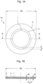
- the Figures show a coin blank 10 including an inner portion 1 and an outer portion 2 surrounding the inner portion 1.
- the inner portion 1 may be a disc which shape may be a regular circle, a circle with scallops, notches or flat portions, an oval, an ellipse, or a regular or irregular polygon with or without rounded corners.
- the inner portion may be a ring with a concentric opening.
- the inner surface of the outer portion 2 may be equidistant to the outer surface of the inner portion 1.
- the contour of the inner surface of the outer portion 2 oriented to the inner portion 1 may be a regular circle, a circle with scallops, notches or flat portions, an oval, an ellipse, or a regular or irregular polygon with or without rounded corners.
- the outer surface of the outer portion 2 may be equidistant to the inner surface and the shapes of the outer and inner surfaces may be the same. According to other embodiments, the outer surface of the outer portion 2 has another shape than the inner surface and the outer portion 2 may have a non-uniform width. For example, the inner surface may have a circular contour and the outer surface may be a polygon.
- the coin blank 10 may include one, two or more outer portions 2, wherein the innermost outer portion 2 surrounds the inner portion 1 and further outer portions 2 surround the respectively preceding outer portion 2.
- the inner portion 1 is a disc which shape is a regular circle and the shape of the outer portion 2 is a concentric regular ring.
- Other examples may provide two, three or more concentric outer portions.
- the inner portion 1 and the outer portion 2 may be arranged in the same plane.
- a thickness dd of the inner portion 1 may be smaller, equal or greater than the thickness dr of the outer portion 2.
- the distance between the disc-like inner portion 1 and the outer portion 2 may be uniform over the complete disc perimeter.
- the distance may be in the range of 0.1 to 5.0 mm. In accordance with an example, the distance is in the range from 0.5 to 3.0 mm.
- the inner portion 1 and the inner diameter of the outer portion 2 are regularly circular and concentric and the distance between the inner portion 1 and the outer portion 2 is uniform over the whole perimeter of the inner portion 1.
- the inner and outer portions 1, 2 may be pure metals, e.g. Cu, metal alloys and/or coated metals. Corpuses of the inner and outer portions 1, 2 may be massive (homogenous) or multi-layered stacks with cladded, coated or electroplated layers. According to an example, at least one of the materials of the inner portion 1 and the outer portion 2 is a stainless steel, e.g. a ferritic steels, or a copper alloy, for example a copper alloy selected from a group including CuNi, CuAlNi, CuZnNi, CuSn, CuZn, CuAlZnSn.
- An isolation layer 3 fills a gap between the inner portion 1 and the outer portion 2 in a permanently force-locking manner.
- the isolation layer 3 is provided from a dielectric insulating material.
- the isolation layer 3 is formed from a transparent material.
- Conventional bimetallic coins may be mixed up optically with bimetallic coins having another face value or with foreign currency values because of too little differences in seize, engraving (stamping) and colour nuances.
- a transparent isolation layer 3 provides a further significant optical characteristic that increases the differences among multipart coins of different currencies and face values. The transparency of the isolation layer 3 supports a better visual differentiation at cash payment transactions, by way of example.
- the isolation layer 3 may be based on a break-proof silicate or ceramic base material.
- the isolation layer 3 contains or consists of a polymer or a composite material, which is thermal stable at least in the conventional temperature range for coins.
- the material of the isolation layer 3 may be thermal stable even above 150 degree Celsius up to at least 200 degree Celsius.
- the width of the isolation layer 3 may be in the range from 0.5 to 3.0 mm to allow good optical perception of the isolation layer 3 during out-of-pocket payments and without the coin loosing the typical grip.
- the isolation layer 3 is based on a polymer that contains sulphur, e.g. poly sulphone, or ether ketone, like polyether ether ketone (PEEK).
- PEEK polyether ether ketone
- Other examples may provide the isolation layer 3 from a composite material containing an organic base material that is doped with one or more inorganic materials.
- the isolation layer 3 contains an organic base material and at least one type of pigments (dye), an ultraviolet (UV) stabilizer, fluorescent components and/or particles generating holographic effects.
- the coin blank 10 may include an inner portion 1 and an outer portion 2 surrounding the inner portion 1.
- An isolation layer 3 is arranged between the inner portion 1 and the outer portion 2 and connects the inner portion 1 and the outer portion 2 in a force-locking manner.
- the isolation layer 3 is to a high degree transparent in a first wavelength range, for example the visible wavelength range, and to a high degree opaque i.e. absorbant in a second wavelength range, for example the near infrared range.
- the first wavelength range may be or may include wavelength ranges outside the visible wavelength range, for example portions of the UV and/or IR range next to the visible wavelength range.
- the first wavelength range is a visible wavelength range, e.g. a portion of the visible wavelength range or the complete visible wavelength range.
- the second wavelength range may be or may include a visible wavelength range, e.g. a portion of the visible wavelength range or the complete visible wavelength range.
- the second wavelength range may be or may include wavelength ranges outside the visible wavelength range, for example portions of the UV and/or IR range next to the visible wavelength range, e.g. NIR.
- coin identification stages distinguish coins from other objects inserted in the coin slot of an apparatus like a coin-operating machine or coin validator.
- the coin identification stage may include a photo sensor sampling the size of an object passing the coin slot.
- photo sensors to detect the coin position during coin handling in the apparatus or to confirm that the coin leaves the exit of the apparatus.
- the coin identification stage may wrongly interpret the isolation layer 3 as a gap between two objects and hence may detect three objects instead of one bimetallic coin.
- the wavelength selective transparency of the isolation layer 3 allows for an automatic optic detection of such coins in coin validators and coin operated machines, which use a certain wavelength range, e.g. the near infrared range, for coin identification, without loosing the transparency in another wavelength range, e.g. the visual wavelength range.
- the shape of the inner portion 1 may be a circle and the outer portion 2 may be a ring concentric with the inner portion 1.
- the second wavelength range may be a near infrared range including at least the wavelength range from 700 nm to 1100 nm.
- the first wavelength range may be a visible wavelength range including at least portions of the wavelength range from 400 to 700 nm.
- the transmittance in the visible wavelength range may vary from 50 % to at least 90 %.
- the transmittance in the first wavelength range e.g. the visible wavelength range, may be more than 90 % or 95 %.
- the absorptance (attenuation factor) in the second wavelength range e.g.
- the isolation layer 3 may be based on a transparent polymer and may contain additives absorbing or reflecting light in a near infrared range by at least 80 %.
- the additive may include particles of one or more metal oxides.
- the metal oxides may be selected from a group including zinc oxide and aluminium-doped zinc oxide.
- the additive may be a conducting polymer.
- the conducting polymer may be selected from a group including polythiopene and lanthanide bisphthalo cyanine.
- the additive may be an organic compound containing metal complexes absorbing in the near infrared range.
- the metal complexes may be mixed-valence binuclear metal complexes.
- the weight component of the additives is at most 5 % to maintain the transparent characteristic in the visible wavelength range.
- the width w of the isolation layer 3 between the inner and the outer portions 1, 2 may be between 0.3 mm and 5 mm. According to an example the width w is at least 0.50 mm to facilitate a safe detection of the isolation layer 3 in coin validators and coin operated machines providing photo sensors for coin detection. The width w may be at most 3.0 mm to ensure a reliable mechanical connection between the inner and outer portions 1, 2. According to other examples the width w of the isolation layer 3 is selected within a range from 0.5 mm to 3.0 mm by considering the characteristics of the inner and outer portions 1, 2.
- the width of the isolation layer 3 is selected on the basis of material properties of the inner and outer portions 1, 2.
- the electric conductivity Cl of the inner portion 1 is at most half of the electric conductivity CO of the outer portion 2 and the width w of the isolation layer 3 is at least 0.5 mm because safe detection is possible even for smaller widths..
- the electric conductivity Cl of the inner portion 1 is at least twice the electric conductivity CO of the outer portion 2 and the width of the isolation layer 3 is at least 1.0 mm to facilitate safe detection of the isolation layer 3 If the electric conductivities Cl, CO of the inner and outer portions 1, 2 deviate from each other by no more than 50% and the IACS (international annealed copper standard) value is below 10 %, the width w of the isolation layer 3 is at least 1.0 mm. If the electric conductivities Cl, CO of the inner and outer portions 1, 2 deviate from each other by no more than 50% and the IACS (international annealed copper standard) value is 10 % or more, the width w of the isolation layer 3 is at least 0.5 mm.
- the width w of the isolation layer 3 is selected on the basis of the coin geometry to support a safe identification of coin type and face value.
- coin operated machines and coin validators use inductive sensors for identifying the materials of the coin.
- Inner and outer portions 1, 2 deliver a respective inductive signature and the isolation layer 3 provides a certain separation of the signatures. A sufficient separation eases the evaluation and identification of the signatures.
- the width w of the isolation layer 3 is selected considering the diameter DC of the coin blank and the diameter of the inner portion 1. According to an example referring to coin diameters DC from 19 mm to 33 mm and a ratio of the diameter of the inner portion 1 to the coin diameter DC between 50 % and 70 %, e.g. approximately 60 %, the width w may be selected according to equation (1).
- the width w of the isolation layer 3 may be in the range from 0.6 mm to 0.7 mm.
- the width w of the isolation layer 3 may be in the range from 1.6 mm to 2.7 mm.
- the width w of the isolation layer 3 is at least 0.5 mm.
- the coin blank includes at least one further outer portion 2 separated by the preceding outer portion 2 by a further isolation layer 3 having the characteristics of the isolation layer 3 between the inner portion 1 and the outer portion 2.
- a further example relates to a coin which may be a currency coin or a medal.
- the coin includes the coin blank as discussed above and a stamping stamped on at least one side of at least one of the inner and outer portions 1,2.
- the following examples refer to coins or coin blanks including an inner portion 1, at least one outer portion 2 surrounding the inner portion 1, and a dielectric isolation layer 3 between the inner portion 1 and the outer portion 2 and connecting the inner portion 1 and the outer portion 2 in a force-locking manner, wherein a width w of the isolation layer 3 is selected on the basis of properties, e.g. material properties and geometry, of the inner and outer portions 1, 2.
- the isolation layer 3 may be transparent in at least portions of the visible wavelength range, in the complete visible wavelength range and/or in wavelength ranges next to the visible wavelength range, e.g. in the UV range and/or in at least a portion of the IR range, e.g. in the NIR.
- the electric conductivity Cl of the inner portion 1 is at least twice the electric conductivity CO of the outer portion 2 and the width w of the isolation layer 3 is at least 1.0 mm to facilitate safe detection of the isolation layer 3.
- the electric conductivity Cl of the inner portion 1 is at most half of the electric conductivity CO of the outer portion 2 and the width wof the isolation layer 3 is at least 0.5 mm, because safe detection is possible even for smaller widths.
- the width w of the isolation layer 3 is at least 1.0 mm. If the electric conductivities of the inner and outer portions 1, 2 deviate from each other by no more than 50% and the IACS (international annealed copper standard) value is 10 % or more, the width w of the isolation layer 3 is at least 0.5 mm.
- the width w of the isolation layer 3 is selected on the basis of the coin geometry to support a safe identification of coin type and face value.
- coin operated machines and coin validators use inductive sensors for identifying the materials of the coin.
- Inner and outer portions 1, 2 deliver a respective inductive signature and the isolation layer 3 provides a certain separation of the signatures. A sufficient separation eases the evaluation and identification of the signatures.
- the width w of the isolation layer 3 is selected considering the diameter DC of the coin and the diameter of the inner portion 1. According to an example referring to coin diameters DC from 19 mm to 33 mm and a ratio of the diameter of the inner portion 1 to the coin diameter DC between 50 % and 70 %, e.g. approximately 60 %, the width w may be selected according to equation (1) above.
- the width w of the isolation layer 3 may be in the range from 0.6 mm to 0.7 mm.
- the width w of the isolation layer 3 may be in the range from 1.6 mm to 2.7 mm.
- the width w of the isolation layer 3 is at least 0.5 mm.
- a bimetallic coin consists of a disc-shaped inner portion and a concentric, annular-shaped outer portion, which form a permanently connected composite on which a face value provided for the coin is stamped.
- An isolation layer is concentrically arranged between the inner portion and the outer portion in a force-locking manner.
- the isolation layer consists of a polymer or a composite material.
- the polymer may be a polymer containing sulphur or an etherketone-containing polymer.
- a polysulphone (PSU) or a polyether etherketone (PEEK) is used.
- the composite material may consist of an organic base material which is doped with an inorganic material. Pigments, UV-stabilizers, fluorescent components and/or particles with holographic imaging may be used as inorganic material.
- the composite material may consist of amorphous silicate or ceramic base materials.
- the isolation layer withstands temperatures above 150 degree Celsius.
- the isolation layer has transparent, semi-transparent (translucent), opalescent characteristics and/or includes colour effects.
- the width of the isolation layer between the disc and the ring ranges from 0.5 mm to 3.0 mm.
- the isolation layer is deformable by a stamping process applied to provide a currency coin from the coin blank.
Landscapes
- Physics & Mathematics (AREA)
- General Physics & Mathematics (AREA)
- Testing Of Coins (AREA)
- Adornments (AREA)
- Laminated Bodies (AREA)
- Illuminated Signs And Luminous Advertising (AREA)
- Control Of Vending Devices And Auxiliary Devices For Vending Devices (AREA)
- Inspection Of Paper Currency And Valuable Securities (AREA)
Priority Applications (1)
| Application Number | Priority Date | Filing Date | Title |
|---|---|---|---|
| EP19212775.1A EP3646750B1 (en) | 2012-07-30 | 2012-07-30 | Multipart coin blank and coin |
Applications Claiming Priority (3)
| Application Number | Priority Date | Filing Date | Title |
|---|---|---|---|
| PCT/EP2012/003239 WO2014019593A1 (en) | 2012-07-30 | 2012-07-30 | Multipart coin blank and coin |
| EP19212775.1A EP3646750B1 (en) | 2012-07-30 | 2012-07-30 | Multipart coin blank and coin |
| EP12742808.4A EP2709483B1 (en) | 2012-07-30 | 2012-07-30 | Multipart coin blank and coin |
Related Parent Applications (1)
| Application Number | Title | Priority Date | Filing Date |
|---|---|---|---|
| EP12742808.4A Division EP2709483B1 (en) | 2012-07-30 | 2012-07-30 | Multipart coin blank and coin |
Publications (3)
| Publication Number | Publication Date |
|---|---|
| EP3646750A1 EP3646750A1 (en) | 2020-05-06 |
| EP3646750B1 true EP3646750B1 (en) | 2025-05-21 |
| EP3646750C0 EP3646750C0 (en) | 2025-05-21 |
Family
ID=46603882
Family Applications (2)
| Application Number | Title | Priority Date | Filing Date |
|---|---|---|---|
| EP19212775.1A Active EP3646750B1 (en) | 2012-07-30 | 2012-07-30 | Multipart coin blank and coin |
| EP12742808.4A Active EP2709483B1 (en) | 2012-07-30 | 2012-07-30 | Multipart coin blank and coin |
Family Applications After (1)
| Application Number | Title | Priority Date | Filing Date |
|---|---|---|---|
| EP12742808.4A Active EP2709483B1 (en) | 2012-07-30 | 2012-07-30 | Multipart coin blank and coin |
Country Status (20)
Families Citing this family (5)
| Publication number | Priority date | Publication date | Assignee | Title |
|---|---|---|---|---|
| JP6834419B2 (ja) * | 2016-11-30 | 2021-02-24 | 富士電機株式会社 | 硬貨識別装置 |
| PL3764836T3 (pl) * | 2018-03-16 | 2024-04-02 | Monnaie Royale Canadienne/Royal Canadian Mint | Struktura kompozytowa z separatorem do monet i tym podobnych |
| DE102019133806A1 (de) * | 2019-12-10 | 2021-06-10 | B.H. Mayer's Kunstprägeanstalt GmbH | Münze oder Medaille |
| KR102479527B1 (ko) * | 2020-07-06 | 2022-12-19 | 한국조폐공사 | 광결정 소재를 포함하는 광가변부가 적용된 금속가공품 및 그의 제조방법 |
| WO2023037955A1 (ja) * | 2021-09-08 | 2023-03-16 | グローリー株式会社 | 硬貨識別装置、硬貨処理装置及び硬貨識別方法 |
Family Cites Families (23)
| Publication number | Priority date | Publication date | Assignee | Title |
|---|---|---|---|---|
| US800217A (en) * | 1904-05-02 | 1905-09-26 | George B Keplinger | Check or counter. |
| FR1001412A (fr) * | 1946-05-03 | 1952-02-25 | Perfectionnements aux jetons et plaques de jeu | |
| US3983646A (en) * | 1974-08-08 | 1976-10-05 | Gamex Industries Inc. | Chip structure |
| US4026309A (en) * | 1974-08-08 | 1977-05-31 | Gamex Industries Inc. | Chip structure |
| US4827640A (en) * | 1987-04-27 | 1989-05-09 | Jones Bernard B | Gaming token and process therefor |
| US5361885A (en) * | 1993-02-23 | 1994-11-08 | Peter Modler | Anticounterfeiting device for gaming chips |
| US6021882A (en) * | 1998-03-12 | 2000-02-08 | Idx, Inc. | Token having predetermined optical characteristics and a token validation device therefor |
| SE523567C2 (sv) * | 1999-01-08 | 2004-04-27 | Scan Coin Ind Ab | Myntsärskiljande anordning och metod |
| US6352261B1 (en) * | 2000-12-11 | 2002-03-05 | Darrell L. Brown | Casino chip |
| SE522752C2 (sv) * | 2001-11-05 | 2004-03-02 | Scan Coin Ind Ab | Metod att driva en myntdiskriminator och en myntdiskriminator där påverkan på spolorgan mäts när mynt utsätts för magnetfält alstrade av spolorgan utanför myntet |
| JP2004220114A (ja) * | 2003-01-09 | 2004-08-05 | Japan Mint | 貨幣状物、およびその識別方法と識別装置 |
| JP2004233641A (ja) * | 2003-01-30 | 2004-08-19 | Nippon Kayaku Co Ltd | 近赤外線吸収フィルム |
| JP2005293097A (ja) * | 2004-03-31 | 2005-10-20 | Terajima Yoshikazu | コイン判別装置、及びこれを備えた台間貸出機。 |
| JP4665499B2 (ja) * | 2004-12-10 | 2011-04-06 | 三菱マテリアル株式会社 | 金属微粒子とその製造方法とその含有組成物ならびにその用途 |
| JP2006330985A (ja) * | 2005-05-25 | 2006-12-07 | Metal Tec Kk | コイン |
| AU2005290415A1 (en) * | 2005-06-02 | 2006-04-13 | Intect Planning Co., Ltd. | Metal part-containing article, coin and method for manufacturing same |
| US7918455B2 (en) * | 2005-11-09 | 2011-04-05 | Gaming Partners International | Chip with insert including an electronic microchip |
| EP1980586B1 (en) * | 2007-04-12 | 2011-01-26 | Solvay Advanced Polymers, LLC | High-performance polysulfone composition |
| JP2009108407A (ja) * | 2007-10-12 | 2009-05-21 | Fujifilm Corp | 屈曲棒状金属粒子及びその製造方法、並びに屈曲棒状金属粒子含有組成物、及び導電性材料 |
| DE202010018385U1 (de) * | 2010-03-27 | 2016-03-16 | Bayerisches Hauptmünzamt | Bimetallmünze |
| AP2013006863A0 (en) * | 2010-09-17 | 2013-05-31 | Sicpa Holding Sa | Tamperproof case |
| JP5701552B2 (ja) * | 2010-09-24 | 2015-04-15 | カーリットホールディングス株式会社 | 近赤外線吸収色素及び近赤外線遮断フィルター |
| CN102293487B (zh) * | 2011-07-05 | 2013-04-10 | 上海造币有限公司 | 多种金属组合的硬币、章坯饼及制备方法 |
-
2012
- 2012-07-30 BR BR112015001523-9A patent/BR112015001523B1/pt active IP Right Grant
- 2012-07-30 LT LTEP12742808.4T patent/LT2709483T/lt unknown
- 2012-07-30 MX MX2015001042A patent/MX356918B/es active IP Right Grant
- 2012-07-30 JP JP2015524645A patent/JP6542121B2/ja active Active
- 2012-07-30 WO PCT/EP2012/003239 patent/WO2014019593A1/en active Application Filing
- 2012-07-30 HR HRP20200259TT patent/HRP20200259T1/hr unknown
- 2012-07-30 ES ES12742808T patent/ES2769311T3/es active Active
- 2012-07-30 EA EA201590093A patent/EA033487B1/ru not_active IP Right Cessation
- 2012-07-30 SG SG11201500590VA patent/SG11201500590VA/en unknown
- 2012-07-30 CN CN201280075047.3A patent/CN104661555B/zh active Active
- 2012-07-30 HU HUE12742808A patent/HUE048292T2/hu unknown
- 2012-07-30 CA CA2843770A patent/CA2843770C/en active Active
- 2012-07-30 KR KR1020177003273A patent/KR102036557B1/ko active Active
- 2012-07-30 EP EP19212775.1A patent/EP3646750B1/en active Active
- 2012-07-30 KR KR1020157002457A patent/KR20150054759A/ko not_active Ceased
- 2012-07-30 AU AU2012386890A patent/AU2012386890A1/en not_active Abandoned
- 2012-07-30 PL PL12742808T patent/PL2709483T3/pl unknown
- 2012-07-30 PT PT127428084T patent/PT2709483T/pt unknown
- 2012-07-30 EP EP12742808.4A patent/EP2709483B1/en active Active
- 2012-07-30 IN IN511DEN2015 patent/IN2015DN00511A/en unknown
-
2014
- 2014-01-31 US US14/169,228 patent/US20140144751A1/en not_active Abandoned
-
2015
- 2015-01-23 ZA ZA2015/00524A patent/ZA201500524B/en unknown
-
2016
- 2016-11-17 AU AU2016259405A patent/AU2016259405B2/en active Active
-
2017
- 2017-09-22 US US15/712,943 patent/US20180012437A1/en not_active Abandoned
Also Published As
Similar Documents
| Publication | Publication Date | Title |
|---|---|---|
| US20180012437A1 (en) | Multipart coin blank and coin | |
| DE102010013148B4 (de) | Bimetallmünze und Rohling für eine Bimetallmünze | |
| US10479128B2 (en) | Security feature | |
| DE102017116736B3 (de) | Chipkartenmodul, verfahren zum herstellen eines chipkartenmoduls, chipkarte und verfahren zum prüfen eines chipkartenmoduls | |
| US9241548B2 (en) | Coin and method for producing a coin | |
| WO2012156006A1 (de) | Mehrteilige münze mit einem kern aus kunststoff | |
| CN107657304A (zh) | 电子身份证件 | |
| JP6681850B2 (ja) | 硬貨用基体及び硬貨 | |
| EP2143829A2 (en) | Control of electromagnetic signals of coins through multi-ply plating technology | |
| CN111492637B (zh) | 标签剂系统 | |
| KR20210110733A (ko) | 금속의 자기 마킹을 위한 산화물 자성 입자의 사용 |
Legal Events
| Date | Code | Title | Description |
|---|---|---|---|
| PUAI | Public reference made under article 153(3) epc to a published international application that has entered the european phase |
Free format text: ORIGINAL CODE: 0009012 |
|
| STAA | Information on the status of an ep patent application or granted ep patent |
Free format text: STATUS: THE APPLICATION HAS BEEN PUBLISHED |
|
| AC | Divisional application: reference to earlier application |
Ref document number: 2709483 Country of ref document: EP Kind code of ref document: P |
|
| AK | Designated contracting states |
Kind code of ref document: A1 Designated state(s): AL AT BE BG CH CY CZ DE DK EE ES FI FR GB GR HR HU IE IS IT LI LT LU LV MC MK MT NL NO PL PT RO RS SE SI SK SM TR |
|
| STAA | Information on the status of an ep patent application or granted ep patent |
Free format text: STATUS: REQUEST FOR EXAMINATION WAS MADE |
|
| 17P | Request for examination filed |
Effective date: 20201005 |
|
| RBV | Designated contracting states (corrected) |
Designated state(s): AL AT BE BG CH CY CZ DE DK EE ES FI FR GB GR HR HU IE IS IT LI LT LU LV MC MK MT NL NO PL PT RO RS SE SI SK SM TR |
|
| RAP3 | Party data changed (applicant data changed or rights of an application transferred) |
Owner name: MINT OF FINLAND GMBH Owner name: BAYERISCHES HAUPTMUENZAMT Owner name: CRANE PAYMENT INNOVATIONS GMBH Owner name: STAATLICHE MUENZEN BADEN-WUERTTEMBERG MUENZSTAETTE STUTTGART UND MUENZSTAETTE KARLSRUHE |
|
| STAA | Information on the status of an ep patent application or granted ep patent |
Free format text: STATUS: EXAMINATION IS IN PROGRESS |
|
| 17Q | First examination report despatched |
Effective date: 20220804 |
|
| GRAP | Despatch of communication of intention to grant a patent |
Free format text: ORIGINAL CODE: EPIDOSNIGR1 |
|
| STAA | Information on the status of an ep patent application or granted ep patent |
Free format text: STATUS: GRANT OF PATENT IS INTENDED |
|
| INTG | Intention to grant announced |
Effective date: 20231127 |
|
| GRAJ | Information related to disapproval of communication of intention to grant by the applicant or resumption of examination proceedings by the epo deleted |
Free format text: ORIGINAL CODE: EPIDOSDIGR1 |
|
| STAA | Information on the status of an ep patent application or granted ep patent |
Free format text: STATUS: EXAMINATION IS IN PROGRESS |
|
| INTC | Intention to grant announced (deleted) | ||
| GRAP | Despatch of communication of intention to grant a patent |
Free format text: ORIGINAL CODE: EPIDOSNIGR1 |
|
| STAA | Information on the status of an ep patent application or granted ep patent |
Free format text: STATUS: GRANT OF PATENT IS INTENDED |
|
| INTG | Intention to grant announced |
Effective date: 20240524 |
|
| GRAJ | Information related to disapproval of communication of intention to grant by the applicant or resumption of examination proceedings by the epo deleted |
Free format text: ORIGINAL CODE: EPIDOSDIGR1 |
|
| STAA | Information on the status of an ep patent application or granted ep patent |
Free format text: STATUS: EXAMINATION IS IN PROGRESS |
|
| INTC | Intention to grant announced (deleted) | ||
| GRAP | Despatch of communication of intention to grant a patent |
Free format text: ORIGINAL CODE: EPIDOSNIGR1 |
|
| STAA | Information on the status of an ep patent application or granted ep patent |
Free format text: STATUS: GRANT OF PATENT IS INTENDED |
|
| GRAJ | Information related to disapproval of communication of intention to grant by the applicant or resumption of examination proceedings by the epo deleted |
Free format text: ORIGINAL CODE: EPIDOSDIGR1 |
|
| STAA | Information on the status of an ep patent application or granted ep patent |
Free format text: STATUS: EXAMINATION IS IN PROGRESS |
|
| INTG | Intention to grant announced |
Effective date: 20241017 |
|
| INTC | Intention to grant announced (deleted) | ||
| GRAP | Despatch of communication of intention to grant a patent |
Free format text: ORIGINAL CODE: EPIDOSNIGR1 |
|
| STAA | Information on the status of an ep patent application or granted ep patent |
Free format text: STATUS: GRANT OF PATENT IS INTENDED |
|
| INTG | Intention to grant announced |
Effective date: 20241219 |
|
| GRAS | Grant fee paid |
Free format text: ORIGINAL CODE: EPIDOSNIGR3 |
|
| GRAA | (expected) grant |
Free format text: ORIGINAL CODE: 0009210 |
|
| STAA | Information on the status of an ep patent application or granted ep patent |
Free format text: STATUS: THE PATENT HAS BEEN GRANTED |
|
| AC | Divisional application: reference to earlier application |
Ref document number: 2709483 Country of ref document: EP Kind code of ref document: P |
|
| AK | Designated contracting states |
Kind code of ref document: B1 Designated state(s): AL AT BE BG CH CY CZ DE DK EE ES FI FR GB GR HR HU IE IS IT LI LT LU LV MC MK MT NL NO PL PT RO RS SE SI SK SM TR |
|
| REG | Reference to a national code |
Ref country code: GB Ref legal event code: FG4D |
|
| REG | Reference to a national code |
Ref country code: CH Ref legal event code: EP |
|
| REG | Reference to a national code |
Ref country code: DE Ref legal event code: R096 Ref document number: 602012081534 Country of ref document: DE |
|
| REG | Reference to a national code |
Ref country code: IE Ref legal event code: FG4D |
|
| U01 | Request for unitary effect filed |
Effective date: 20250611 |
|
| U07 | Unitary effect registered |
Designated state(s): AT BE BG DE DK EE FI FR IT LT LU LV MT NL PT RO SE SI Effective date: 20250620 |
|
| U20 | Renewal fee for the european patent with unitary effect paid |
Year of fee payment: 14 Effective date: 20250707 |
|
| RAP4 | Party data changed (patent owner data changed or rights of a patent transferred) |
Owner name: SAXONIA EUROCOIN GMBH Owner name: BAYERISCHES HAUPTMUENZAMT Owner name: CRANE PAYMENT INNOVATIONS GMBH Owner name: STAATLICHE MUENZEN BADEN-WUERTTEMBERGMUENZSTAETTE STUTTGART UND MUENZSTAETTE KARLSRUHE |
|
| U1H | Name or address of the proprietor changed after the registration of the unitary effect |
Owner name: SAXONIA EUROCOIN GMBH; DE Owner name: BAYERISCHES HAUPTMUENZAMT; DE Owner name: CRANE PAYMENT INNOVATIONS GMBH; DE Owner name: STAATLICHE MUENZEN BADEN-WUERTTEMBERGMUENZSTAETTE STUTTGART UND MUENZSTAETTE KARLSRUHE; DE |