EP3641502B1 - Interface circuit - Google Patents
Interface circuit Download PDFInfo
- Publication number
- EP3641502B1 EP3641502B1 EP19209235.1A EP19209235A EP3641502B1 EP 3641502 B1 EP3641502 B1 EP 3641502B1 EP 19209235 A EP19209235 A EP 19209235A EP 3641502 B1 EP3641502 B1 EP 3641502B1
- Authority
- EP
- European Patent Office
- Prior art keywords
- string
- terminal
- interface circuit
- switching element
- light source
- Prior art date
- Legal status (The legal status is an assumption and is not a legal conclusion. Google has not performed a legal analysis and makes no representation as to the accuracy of the status listed.)
- Active
Links
Images


Classifications
-
- H—ELECTRICITY
- H05—ELECTRIC TECHNIQUES NOT OTHERWISE PROVIDED FOR
- H05B—ELECTRIC HEATING; ELECTRIC LIGHT SOURCES NOT OTHERWISE PROVIDED FOR; CIRCUIT ARRANGEMENTS FOR ELECTRIC LIGHT SOURCES, IN GENERAL
- H05B45/00—Circuit arrangements for operating light-emitting diodes [LED]
- H05B45/30—Driver circuits
- H05B45/37—Converter circuits
-
- H—ELECTRICITY
- H05—ELECTRIC TECHNIQUES NOT OTHERWISE PROVIDED FOR
- H05B—ELECTRIC HEATING; ELECTRIC LIGHT SOURCES NOT OTHERWISE PROVIDED FOR; CIRCUIT ARRANGEMENTS FOR ELECTRIC LIGHT SOURCES, IN GENERAL
- H05B45/00—Circuit arrangements for operating light-emitting diodes [LED]
- H05B45/40—Details of LED load circuits
- H05B45/44—Details of LED load circuits with an active control inside an LED matrix
-
- H—ELECTRICITY
- H05—ELECTRIC TECHNIQUES NOT OTHERWISE PROVIDED FOR
- H05B—ELECTRIC HEATING; ELECTRIC LIGHT SOURCES NOT OTHERWISE PROVIDED FOR; CIRCUIT ARRANGEMENTS FOR ELECTRIC LIGHT SOURCES, IN GENERAL
- H05B45/00—Circuit arrangements for operating light-emitting diodes [LED]
- H05B45/30—Driver circuits
- H05B45/37—Converter circuits
- H05B45/3725—Switched mode power supply [SMPS]
-
- H—ELECTRICITY
- H05—ELECTRIC TECHNIQUES NOT OTHERWISE PROVIDED FOR
- H05B—ELECTRIC HEATING; ELECTRIC LIGHT SOURCES NOT OTHERWISE PROVIDED FOR; CIRCUIT ARRANGEMENTS FOR ELECTRIC LIGHT SOURCES, IN GENERAL
- H05B45/00—Circuit arrangements for operating light-emitting diodes [LED]
- H05B45/60—Circuit arrangements for operating LEDs comprising organic material, e.g. for operating organic light-emitting diodes [OLED] or polymer light-emitting diodes [PLED]
-
- H—ELECTRICITY
- H05—ELECTRIC TECHNIQUES NOT OTHERWISE PROVIDED FOR
- H05B—ELECTRIC HEATING; ELECTRIC LIGHT SOURCES NOT OTHERWISE PROVIDED FOR; CIRCUIT ARRANGEMENTS FOR ELECTRIC LIGHT SOURCES, IN GENERAL
- H05B45/00—Circuit arrangements for operating light-emitting diodes [LED]
- H05B45/30—Driver circuits
- H05B45/37—Converter circuits
- H05B45/3725—Switched mode power supply [SMPS]
- H05B45/39—Circuits containing inverter bridges
-
- Y—GENERAL TAGGING OF NEW TECHNOLOGICAL DEVELOPMENTS; GENERAL TAGGING OF CROSS-SECTIONAL TECHNOLOGIES SPANNING OVER SEVERAL SECTIONS OF THE IPC; TECHNICAL SUBJECTS COVERED BY FORMER USPC CROSS-REFERENCE ART COLLECTIONS [XRACs] AND DIGESTS
- Y02—TECHNOLOGIES OR APPLICATIONS FOR MITIGATION OR ADAPTATION AGAINST CLIMATE CHANGE
- Y02B—CLIMATE CHANGE MITIGATION TECHNOLOGIES RELATED TO BUILDINGS, e.g. HOUSING, HOUSE APPLIANCES OR RELATED END-USER APPLICATIONS
- Y02B20/00—Energy efficient lighting technologies, e.g. halogen lamps or gas discharge lamps
- Y02B20/30—Semiconductor lamps, e.g. solid state lamps [SSL] light emitting diodes [LED] or organic LED [OLED]
Definitions
- the invention relates to an interface circuit for operating a light source by making use of a high frequency fluorescent lamp driver, and a corresponding method of operating a light source by making use of a high frequency fluorescent lamp driver.
- Fluorescent lamps are highly efficient light sources that have been in use for many years.
- the efficiency and lifetime of fluorescent lamps are particularly high when they are driven by an electronic lamp driver that supplies a high frequency lamp current with a frequency in the order of 10 kHz.
- luminaires comprising such a high frequency fluorescent lamp driver are present in homes and offices all over the world.
- alternative electrically powered light sources in the form of LEDs and OLEDs or high pressure discharge lamps have become available that have an efficiency and a lifetime that is even higher than that of a fluorescent lamp.
- the interface circuit and the light source together must emulate a fluorescent lamp, when the interface circuit and the light source are jointly connected to the lamp connection terminals and the high frequency fluorescent lamp driver goes through the lamp operating stages: preheat, ignition and stationary operation. Furthermore, the interface circuit must convert the high frequency AC voltage supplied by the high frequency lamp driver into a DC-current that supplies the light source.
- the invention aims to provide an interface circuit and a corresponding method that is capable of emulating a fluorescent lamp in a simple and effective way.
- an interface circuit for operating a light source is according to claim 1 and a method of use according to claim 10.
- the high frequency fluorescent lamp driver In the case that a fluorescent lamp is connected to a high frequency fluorescent lamp driver, the high frequency fluorescent lamp driver generates a high frequency voltage with a comparatively high amplitude across the fluorescent lamp during the ignition phase. When the fluorescent lamp ignites, the voltage across the lamp decreases strongly and the lamp carries a current. In reaction to the ignition (detected by the voltage drop or the presence of a lamp current), the high frequency fluorescent lamp driver changes its operation state from ignition to stationary operation by changing its frequency of operation and supplies a high frequency AC current to the lamp. In the case of an interface circuit according to the invention being connected to the high frequency fluorescent lamp driver, the sensor circuit detects the ignition voltage that has an amplitude higher than the predetermined value and renders the first switching element comprised in the third string conductive.
- the first switching element controls the conductive state of the third string.
- the voltage between the first and second terminal drops and the light source starts carrying current.
- the high frequency fluorescent lamp driver is thereby triggered to change its operating state from ignition to stationary operation and supplies a high frequency current to the third string, that is rectified by the rectifier and subsequently supplied to the light source.
- the ignition of the lamp is emulated in a simple and effective manner.
- the interface circuit comprises a DC-DC-converter coupled, during operation, between output terminals of the rectifier and the light source.
- the DC-DC-converter can for instance be an up-converter, a down converter or a fly-back converter. Such converters are well known in the art and need not be further discussed.
- the DC-DC-converter converts the voltage across the third string, that approximately equals the voltage across a burning fluorescent lamp, into a voltage that matches the voltage across the light source when it carries current.
- the light source need not be constructed such that, in operation, the voltage across it exactly matches the voltage across a burning fluorescent lamp.
- the light source is a high pressure discharge lamp
- a commutator such as a full bridge between the DC-DC-converter and the light source to commutate the DC-current supplied by the DC-DC-converter.
- the interface circuit needs to be equipped with, for instance, a separate igniter.
- Full bridge commutator circuits and igniter circuits are well known in the art and need not be further discussed.
- the interface circuit comprises a capacitor that, during operation, shunts the light source.
- the capacitor By virtue of the capacitor, the amplitude of the current through the light source changes less during a period of the high frequency current generated by the high frequency fluorescent lamp driver, so that the same is true for the light output of the light source.
- the interface circuit according to the invention is equipped with a fifth string connected in parallel to the third string and comprising an impedance and a further switching element having its control electrode coupled to an output terminal of the sensor circuit.
- the interface circuit may be equipped with a fifth string comprising an impedance and a further switching element and being coupled between output terminals of the rectifier comprised in the third string.
- a control electrode of the further switching element is coupled to an output terminal of the sensor circuit.
- the interface circuit may be equipped with a fifth string coupled between input terminals of the rectifier comprised in the first string and comprising an impedance.
- the impedance will carry current during operation of the light source. Since the high frequency fluorescent lamp driver acts as a current source, the impedance lowers the current through the light source and thereby also the amount of power consumed by the light source. A proper choice of the impedance value thus enables a proper match to be achieved between the power that the LED-array is designed to consume and the power that the high frequency fluorescent lamp driver is designed to supply. Instabilities are thereby avoided.
- the impedance may be a resistor. However, a reactive element, more in particular a capacitor, is preferred to minimize power dissipation.
- the light source is preferably one of the group formed by LED, OLED and high pressure discharge lamp.
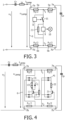
- FIGs. 4-6 show embodiments of an interface circuit according to the invention with a light source connected thereto.
- Figures 1-3 show examples useful to understand the invention.
- the terminals 1 are terminals comprised in a high frequency fluorescent lamp driver.
- Cr and Lr are a DC-blocking capacitor and a resonant choke, respectively, that are part of the high frequency fluorescent lamp driver.
- Reference numerals 7a and 7b are a first pair of input terminals and a second pair of input terminals, respectively, of the interface circuit, that are connected to lamp connection terminals of the high frequency fluorescent lamp driver.
- Reference numeral 5a is a first string interconnecting the first pair of input terminals 7a.
- Reference numeral 5b is a second string interconnecting the second pair of input terminals. Both strings comprise a series arrangement of two resistors, each having a resistance equal to half the resistance (Rf/2) of a filament of a fluorescent lamp.
- Capacitor Cp connects an input terminal of the first pair to an input terminal of the second pair. Capacitor Cp is also part of the high frequency fluorescent lamp driver.
- a common terminal of the resistors comprised in the first string forms a first terminal T1 of the first string and a common terminal of the resistors comprised in the second string forms a second terminal T2.
- the first and the second terminal are interconnected by a third string comprising a first switching element 11 and a circuit part 9 that comprises a rectifier.
- Circuit part 9 is coupled to light source 10.
- Light source 10 may be an array of LEDs or OLEDs or a high pressure discharge lamp.
- circuit part 9 may comprise additional circuitry such as a DC-DC-converter that, during operation, is coupled between the rectifier and the light source 10.
- the first terminal T1 and the second terminal T2 are also interconnected by means of a fourth string comprising a sensor circuit 8, having an output terminal coupled to a control electrode of the first switching element 11, for sensing the amplitude of the high frequency AC voltage between the first and second terminal and for rendering the first switching element conductive when the amplitude of the high frequency AC voltage reaches a predetermined value.
- Input terminals 7a and 7b, first string 5a, second string 5b, first switching element 11, circuit part 9 and sensor circuit 8 together form an interface circuit 6 for operating a light source.
- the lamp driver When the high frequency fluorescent lamp driver is switched on, the lamp driver enters a first operational state, normally referred to as "preheat", during which a preheat current is generated that flows through the filaments of a connected fluorescent lamp to preheat the electrodes. During this preheat state, the voltage across the lamp is maintained at a comparatively low value to prevent ignition of the lamp. Both the lamp voltage and the preheat current are determined by the operating frequency of the high frequency fluorescent lamp driver. In the case that not a fluorescent lamp but the interface circuit shown in Fig. 1 is connected to the lamp connection terminals, the preheat current flows through the first string, capacitor Cp and the second string. The first and second string thus emulate the filaments of a fluorescent lamp.
- a second operational state "ignition” is entered.
- the operating frequency is adjusted to a value such that an ignition voltage with a comparatively high amplitude is present across the lamp. In the case that the lamp ignites under the influence of this ignition voltage, the voltage across the lamp drops and the lamp starts carrying current.
- a third operational stage “stationary operation” is entered. During this stage, the operating frequency is adjusted such that the lamp is supplied with a current that substantially equals the nominal lamp current. In the case that not a fluorescent lamp but the interface circuit shown in Fig.
- the detector circuit detects that the voltage across the lamp is higher than the predetermined value and renders the first switching element conductive. As a consequence, the voltage across the third string drops and the third string starts carrying current. This is detected by the control circuitry of the high frequency fluorescent lamp driver and the third operational stage "stationary operation" is entered. During this operational stage, a current substantially equal to the nominal lamp current flows through the third string. This current is rectified by the rectifier and supplied directly or via a DC-DC-converter to the light source.
- the embodiment in Fig. 1 comprises a fifth string connected in parallel with the third string and comprising an impedance 22 and a further switching element 21.
- the further switching element is rendered conductive at the same time as the first switching element, so that not only the third string but also the fifth string start carrying current.
- the impedance 22 is dimensioned such that the sum of the current through the third string and the current through the fifth string approximately equals the current through the fluorescent lamp that the high frequency fluorescent lamp driver is designed for. In this way, the interface circuit provides a good emulation of the fluorescent lamp also during stationary operation. As a consequence, the light source operation is stable.
- the embodiment shown in Fig. 3 also comprises a fifth string.
- the fifth string comprises an impedance 22 and is connected between input terminals of the rectifier.
- both the light source 10 and the impedance 22 carry current.
- the impedance 22 is dimensioned such that the sum of the current through the third string and the current through the fifth string approximately equals the current through the fluorescent lamp that the high frequency fluorescent lamp driver is designed for. It is remarked that in the embodiment shown in Fig. 3 , sensor circuit 8 can also be connected in parallel with the first switching element 11.
- the impedance 22 carries an AC-current during operation.
- impedance 22 is preferably a capacitor.
- first switching element 11 in the examples shown in Fig. 1 to Fig. 3 is a bidirectional switch.
- the further switching element in the embodiment shown in Fig. 2 is also a bidirectional switch.
- the first and further switching elements comprised in the embodiments shown in Fig. 4 to Fig. 6 are unidirectional switching elements.
- Reference numeral 31 is a rectifier in the form of a diode bridge.
- a LED array 10 is shunted by a capacitor C1 and connected in series with a first switching element 11 between output terminals of the diode bridge 31.
- the output terminals of the diode bridge are also interconnected by means of a fourth string comprising a sensor circuit 8, of which an output is coupled to a control electrode of the first switching element 11.
- the fifth string comprises a rectifier 41 and a series arrangement of an impedance 22 and a further switching element 21, connected to output terminals of rectifier 41.
- a control electrode of further switching element 21 is connected to the output of sensor circuit 8.
- sensor circuit 8 senses a voltage amplitude higher than the predetermined value, it renders the first switch 11 and the further switch 21 conductive.
- LED-array 10, impedance 22 and both switching elements 11 and 21 carry current.
- Impedance 22 is dimensioned such that the sum of the currents through the third and fifth string match the lamp current of the fluorescent lamp that the high frequency fluorescent lamp driver is designed for.
- impedance 22 carries a DC-current and can be implemented as an ohmic resistor.
- the embodiment shown in Fig. 5 differs from that shown in Fig. 4 in that the rectifier 41 is dispensed with and the series arrangement of impedance 22 and further switching element 21 forms a fifth string that interconnects the output terminals of the rectifier 31.
- the control electrode of the further switching element 21 is connected to an output terminal of sensor circuit 8.
- sensor circuit 8 senses a voltage amplitude higher than the predetermined value, it renders the first switch 11 and the further switch 21 conductive.
- LED-array 10, impedance 22 and both switching elements 11 and 21 carry current.
- Impedance 22 is dimensioned such that the sum of the currents through the third and the fifth string match the lamp current of the fluorescent lamp that the high frequency fluorescent lamp driver is designed for. Also in the embodiment shown in Fig. 5 , impedance 22 carries a DC-current and can thus be implemented as a resistor.
- the embodiment shown in Fig. 6 differs from that shown in Fig. 4 in that the impedance 22 is connected between first terminal T1 and the rectifier 41.
- the output terminals of the rectifier are connected by means of the further switching element 21.
- the operation of the embodiment shown in Fig. 6 is very similar to that shown in Fig. 4 and that shown in Fig. 5 .
- the only important difference is that impedance 22 carries an AC- current instead of a DC-current during operation.
- the impedance 22 is preferably implemented as a capacitor.
Landscapes
- Circuit Arrangement For Electric Light Sources In General (AREA)
- Circuit Arrangements For Discharge Lamps (AREA)
- Electroluminescent Light Sources (AREA)
- Control Of Indicators Other Than Cathode Ray Tubes (AREA)
Applications Claiming Priority (3)
| Application Number | Priority Date | Filing Date | Title |
|---|---|---|---|
| EP11160370 | 2011-03-30 | ||
| EP12715184.3A EP2692208B1 (en) | 2011-03-30 | 2012-03-27 | Interface circuit |
| PCT/IB2012/051446 WO2012131573A1 (en) | 2011-03-30 | 2012-03-27 | Interface circuit |
Related Parent Applications (1)
| Application Number | Title | Priority Date | Filing Date |
|---|---|---|---|
| EP12715184.3A Division EP2692208B1 (en) | 2011-03-30 | 2012-03-27 | Interface circuit |
Publications (3)
| Publication Number | Publication Date |
|---|---|
| EP3641502A1 EP3641502A1 (en) | 2020-04-22 |
| EP3641502B1 true EP3641502B1 (en) | 2024-07-24 |
| EP3641502C0 EP3641502C0 (en) | 2024-07-24 |
Family
ID=45976447
Family Applications (2)
| Application Number | Title | Priority Date | Filing Date |
|---|---|---|---|
| EP19209235.1A Active EP3641502B1 (en) | 2011-03-30 | 2012-03-27 | Interface circuit |
| EP12715184.3A Active EP2692208B1 (en) | 2011-03-30 | 2012-03-27 | Interface circuit |
Family Applications After (1)
| Application Number | Title | Priority Date | Filing Date |
|---|---|---|---|
| EP12715184.3A Active EP2692208B1 (en) | 2011-03-30 | 2012-03-27 | Interface circuit |
Country Status (8)
| Country | Link |
|---|---|
| US (1) | US9301354B2 (enExample) |
| EP (2) | EP3641502B1 (enExample) |
| JP (1) | JP5952892B2 (enExample) |
| CN (1) | CN103477710B (enExample) |
| BR (1) | BR112013024724A2 (enExample) |
| ES (1) | ES2985531T3 (enExample) |
| RU (1) | RU2604636C2 (enExample) |
| WO (1) | WO2012131573A1 (enExample) |
Families Citing this family (9)
| Publication number | Priority date | Publication date | Assignee | Title |
|---|---|---|---|---|
| US9357600B2 (en) | 2011-08-15 | 2016-05-31 | Koninklijke Philips N.V. | Electronic ballast-compatible lighting driver for light-emitting diode lamp |
| TR201902903T4 (tr) | 2012-07-11 | 2019-03-21 | Signify Holding Bv | Floresan balast ve led arasında sürücü devresi. |
| TWI523580B (zh) * | 2013-02-22 | 2016-02-21 | Compatible with LED ballast with electronic ballast with preheat current | |
| DE102013011821A1 (de) * | 2013-07-15 | 2015-01-15 | Cooper Crouse-Hinds Gmbh | Beleuchtungsvorrichtung |
| CA2925399A1 (en) * | 2013-09-25 | 2015-04-02 | Silicon Hill B.V. | Led lighting system |
| GB2522689A (en) * | 2014-02-03 | 2015-08-05 | David John Powell | Power regulation of LED lighting used to replace fluorescent lighting powered by electronic ballasts |
| EP3275289B1 (en) * | 2015-03-26 | 2024-02-14 | Silicon Hill B.V. | Led lighting system |
| JP6492954B2 (ja) * | 2015-05-15 | 2019-04-03 | 株式会社リコー | 照明灯、照明装置及び点灯制御回路 |
| JP6681592B2 (ja) * | 2015-12-28 | 2020-04-15 | パナソニックIpマネジメント株式会社 | 信号送信装置、信号受信装置、点灯システム及び照明器具、並びに照明システム |
Citations (1)
| Publication number | Priority date | Publication date | Assignee | Title |
|---|---|---|---|---|
| US20100033095A1 (en) * | 2008-02-08 | 2010-02-11 | Innosys, Inc. | Solid State Semiconductor LED Replacement for Fluorescent Lamps |
Family Cites Families (16)
| Publication number | Priority date | Publication date | Assignee | Title |
|---|---|---|---|---|
| US7490957B2 (en) | 2002-11-19 | 2009-02-17 | Denovo Lighting, L.L.C. | Power controls with photosensor for tube mounted LEDs with ballast |
| US20060193131A1 (en) * | 2005-02-28 | 2006-08-31 | Mcgrath William R | Circuit devices which include light emitting diodes, assemblies which include such circuit devices, and methods for directly replacing fluorescent tubes |
| US7911149B2 (en) | 2007-02-19 | 2011-03-22 | Marlex Engineering Inc. | Impedance controlled electronic lamp circuit |
| DE102007015508B4 (de) | 2007-03-28 | 2016-04-28 | Tridonic Gmbh & Co Kg | Digitale Steuerschaltung eines Betriebsgeräts für Leuchtmittel sowie Verfahren zum Betreiben eines Betriebsgerätes |
| US7759880B2 (en) | 2008-02-12 | 2010-07-20 | General Electric Company | Combined ballast for fluorescent lamp and light emitting diode and method of driving same |
| JP2009200257A (ja) * | 2008-02-21 | 2009-09-03 | Sharp Corp | Led駆動回路 |
| ATE535131T1 (de) * | 2008-05-05 | 2011-12-15 | Koninkl Philips Electronics Nv | Led-system |
| US8358056B2 (en) | 2008-10-16 | 2013-01-22 | Kumho Electric Inc. | LED fluorescent lamp |
| TWI425869B (zh) * | 2008-12-31 | 2014-02-01 | Chi Mei Lighting Tech Corp | 照明裝置 |
| US8089213B2 (en) | 2009-02-05 | 2012-01-03 | Myung Koo Park | LED fluorescent lamp |
| KR100933076B1 (ko) * | 2009-02-05 | 2009-12-21 | 금호전기주식회사 | Led 형광램프 |
| JP2011044316A (ja) * | 2009-08-20 | 2011-03-03 | Panasonic Electric Works Co Ltd | 照明装置 |
| US8729809B2 (en) * | 2009-09-08 | 2014-05-20 | Denovo Lighting, Llc | Voltage regulating devices in LED lamps with multiple power sources |
| DE102010003266A1 (de) * | 2010-03-25 | 2011-09-29 | Osram Gesellschaft mit beschränkter Haftung | Schaltungsanordnung zum Betreiben einer Retrofitlampe und Retrofitlampe |
| JP5708371B2 (ja) * | 2010-10-28 | 2015-04-30 | ミツミ電機株式会社 | 照明用電源装置および保持電流の制御方法 |
| US8581498B1 (en) * | 2011-02-14 | 2013-11-12 | Jade Sky Technologies, Inc. | Control of bleed current in drivers for dimmable lighting devices |
-
2012
- 2012-03-27 EP EP19209235.1A patent/EP3641502B1/en active Active
- 2012-03-27 US US14/008,580 patent/US9301354B2/en active Active
- 2012-03-27 JP JP2014501761A patent/JP5952892B2/ja active Active
- 2012-03-27 CN CN201280016137.5A patent/CN103477710B/zh active Active
- 2012-03-27 ES ES19209235T patent/ES2985531T3/es active Active
- 2012-03-27 WO PCT/IB2012/051446 patent/WO2012131573A1/en not_active Ceased
- 2012-03-27 BR BR112013024724A patent/BR112013024724A2/pt not_active Application Discontinuation
- 2012-03-27 RU RU2013148126/07A patent/RU2604636C2/ru active
- 2012-03-27 EP EP12715184.3A patent/EP2692208B1/en active Active
Patent Citations (1)
| Publication number | Priority date | Publication date | Assignee | Title |
|---|---|---|---|---|
| US20100033095A1 (en) * | 2008-02-08 | 2010-02-11 | Innosys, Inc. | Solid State Semiconductor LED Replacement for Fluorescent Lamps |
Also Published As
| Publication number | Publication date |
|---|---|
| RU2013148126A (ru) | 2015-05-10 |
| EP2692208A1 (en) | 2014-02-05 |
| CN103477710B (zh) | 2016-12-28 |
| EP3641502C0 (en) | 2024-07-24 |
| WO2012131573A1 (en) | 2012-10-04 |
| ES2985531T3 (es) | 2024-11-06 |
| EP2692208B1 (en) | 2019-11-27 |
| RU2604636C2 (ru) | 2016-12-10 |
| BR112013024724A2 (pt) | 2016-12-20 |
| US20140021871A1 (en) | 2014-01-23 |
| JP5952892B2 (ja) | 2016-07-13 |
| EP3641502A1 (en) | 2020-04-22 |
| CN103477710A (zh) | 2013-12-25 |
| US9301354B2 (en) | 2016-03-29 |
| JP2014514696A (ja) | 2014-06-19 |
Similar Documents
| Publication | Publication Date | Title |
|---|---|---|
| EP3641502B1 (en) | Interface circuit | |
| US10989365B2 (en) | LED tube lamp for operating in different modes | |
| US9756698B2 (en) | LED tube lamp with two operating modes compatible with electrical ballasts | |
| US10448479B2 (en) | LED tube lamp | |
| WO2004010735A3 (en) | Lighting control system with variable arc control including start-up circuit for providing a bias voltage supply | |
| US6657401B2 (en) | Ballast for discharge lamp | |
| CN109315039B (zh) | 具有闪烁减少电路的与镇流器无关的改进型led灯 | |
| EP2823691A1 (en) | Led light source | |
| US10667344B2 (en) | Retrofit LED lamp | |
| JP2010182656A (ja) | 蛍光ランプ形状のledランプ | |
| US11841113B2 (en) | LED lamp and its power source module | |
| KR20120124756A (ko) | 엘이디 램프 | |
| JP2016535406A (ja) | 少なくとも1つの第1ledカスケードと、少なくとも1つの第2ledカスケードとを動作させるための回路装置 | |
| WO2016192987A1 (en) | Led light source with improved glow reduction | |
| WO2019206932A1 (en) | Retrofit led lamp | |
| CN209105475U (zh) | Led灯 | |
| EP3376829B1 (en) | Led lamp arrangement for replacing a fluorescent lamp | |
| JP5457875B2 (ja) | 点灯装置及びそれを用いた照明器具 | |
| CN110351920A (zh) | 驱动器和照明模块 | |
| JP2014120223A (ja) | 高圧放電灯点灯装置及び照明器具 | |
| JP2010097698A (ja) | 低効率状態の際にオフを可能にする放電ランプの調光回路 |
Legal Events
| Date | Code | Title | Description |
|---|---|---|---|
| PUAI | Public reference made under article 153(3) epc to a published international application that has entered the european phase |
Free format text: ORIGINAL CODE: 0009012 |
|
| STAA | Information on the status of an ep patent application or granted ep patent |
Free format text: STATUS: THE APPLICATION HAS BEEN PUBLISHED |
|
| AC | Divisional application: reference to earlier application |
Ref document number: 2692208 Country of ref document: EP Kind code of ref document: P |
|
| AK | Designated contracting states |
Kind code of ref document: A1 Designated state(s): AL AT BE BG CH CY CZ DE DK EE ES FI FR GB GR HR HU IE IS IT LI LT LU LV MC MK MT NL NO PL PT RO RS SE SI SK SM TR |
|
| STAA | Information on the status of an ep patent application or granted ep patent |
Free format text: STATUS: REQUEST FOR EXAMINATION WAS MADE |
|
| 17P | Request for examination filed |
Effective date: 20201022 |
|
| RBV | Designated contracting states (corrected) |
Designated state(s): AL AT BE BG CH CY CZ DE DK EE ES FI FR GB GR HR HU IE IS IT LI LT LU LV MC MK MT NL NO PL PT RO RS SE SI SK SM TR |
|
| STAA | Information on the status of an ep patent application or granted ep patent |
Free format text: STATUS: EXAMINATION IS IN PROGRESS |
|
| 17Q | First examination report despatched |
Effective date: 20211102 |
|
| REG | Reference to a national code |
Ref country code: DE Ref legal event code: R079 Ref document number: 602012080963 Country of ref document: DE Free format text: PREVIOUS MAIN CLASS: H05B0033080000 Ipc: H05B0045440000 Ref country code: DE Ref legal event code: R079 Free format text: PREVIOUS MAIN CLASS: H05B0033080000 Ipc: H05B0045440000 |
|
| GRAP | Despatch of communication of intention to grant a patent |
Free format text: ORIGINAL CODE: EPIDOSNIGR1 |
|
| STAA | Information on the status of an ep patent application or granted ep patent |
Free format text: STATUS: GRANT OF PATENT IS INTENDED |
|
| RIC1 | Information provided on ipc code assigned before grant |
Ipc: H05B 45/3725 20200101ALI20240205BHEP Ipc: H05B 45/44 20200101AFI20240205BHEP |
|
| INTG | Intention to grant announced |
Effective date: 20240221 |
|
| GRAS | Grant fee paid |
Free format text: ORIGINAL CODE: EPIDOSNIGR3 |
|
| GRAA | (expected) grant |
Free format text: ORIGINAL CODE: 0009210 |
|
| STAA | Information on the status of an ep patent application or granted ep patent |
Free format text: STATUS: THE PATENT HAS BEEN GRANTED |
|
| AC | Divisional application: reference to earlier application |
Ref document number: 2692208 Country of ref document: EP Kind code of ref document: P |
|
| AK | Designated contracting states |
Kind code of ref document: B1 Designated state(s): AL AT BE BG CH CY CZ DE DK EE ES FI FR GB GR HR HU IE IS IT LI LT LU LV MC MK MT NL NO PL PT RO RS SE SI SK SM TR |
|
| REG | Reference to a national code |
Ref country code: GB Ref legal event code: FG4D |
|
| REG | Reference to a national code |
Ref country code: CH Ref legal event code: EP |
|
| REG | Reference to a national code |
Ref country code: DE Ref legal event code: R096 Ref document number: 602012080963 Country of ref document: DE |
|
| REG | Reference to a national code |
Ref country code: IE Ref legal event code: FG4D |
|
| U01 | Request for unitary effect filed |
Effective date: 20240822 |
|
| U07 | Unitary effect registered |
Designated state(s): AT BE BG DE DK EE FI FR IT LT LU LV MT NL PT RO SE SI Effective date: 20240902 |
|
| REG | Reference to a national code |
Ref country code: ES Ref legal event code: FG2A Ref document number: 2985531 Country of ref document: ES Kind code of ref document: T3 Effective date: 20241106 |
|
| PG25 | Lapsed in a contracting state [announced via postgrant information from national office to epo] |
Ref country code: NO Free format text: LAPSE BECAUSE OF FAILURE TO SUBMIT A TRANSLATION OF THE DESCRIPTION OR TO PAY THE FEE WITHIN THE PRESCRIBED TIME-LIMIT Effective date: 20241024 |
|
| PG25 | Lapsed in a contracting state [announced via postgrant information from national office to epo] |
Ref country code: GR Free format text: LAPSE BECAUSE OF FAILURE TO SUBMIT A TRANSLATION OF THE DESCRIPTION OR TO PAY THE FEE WITHIN THE PRESCRIBED TIME-LIMIT Effective date: 20241025 Ref country code: PL Free format text: LAPSE BECAUSE OF FAILURE TO SUBMIT A TRANSLATION OF THE DESCRIPTION OR TO PAY THE FEE WITHIN THE PRESCRIBED TIME-LIMIT Effective date: 20240724 |
|
| PG25 | Lapsed in a contracting state [announced via postgrant information from national office to epo] |
Ref country code: IS Free format text: LAPSE BECAUSE OF FAILURE TO SUBMIT A TRANSLATION OF THE DESCRIPTION OR TO PAY THE FEE WITHIN THE PRESCRIBED TIME-LIMIT Effective date: 20241124 |
|
| PG25 | Lapsed in a contracting state [announced via postgrant information from national office to epo] |
Ref country code: HR Free format text: LAPSE BECAUSE OF FAILURE TO SUBMIT A TRANSLATION OF THE DESCRIPTION OR TO PAY THE FEE WITHIN THE PRESCRIBED TIME-LIMIT Effective date: 20240724 |
|
| PG25 | Lapsed in a contracting state [announced via postgrant information from national office to epo] |
Ref country code: RS Free format text: LAPSE BECAUSE OF FAILURE TO SUBMIT A TRANSLATION OF THE DESCRIPTION OR TO PAY THE FEE WITHIN THE PRESCRIBED TIME-LIMIT Effective date: 20241024 |
|
| PG25 | Lapsed in a contracting state [announced via postgrant information from national office to epo] |
Ref country code: RS Free format text: LAPSE BECAUSE OF FAILURE TO SUBMIT A TRANSLATION OF THE DESCRIPTION OR TO PAY THE FEE WITHIN THE PRESCRIBED TIME-LIMIT Effective date: 20241024 Ref country code: PL Free format text: LAPSE BECAUSE OF FAILURE TO SUBMIT A TRANSLATION OF THE DESCRIPTION OR TO PAY THE FEE WITHIN THE PRESCRIBED TIME-LIMIT Effective date: 20240724 Ref country code: NO Free format text: LAPSE BECAUSE OF FAILURE TO SUBMIT A TRANSLATION OF THE DESCRIPTION OR TO PAY THE FEE WITHIN THE PRESCRIBED TIME-LIMIT Effective date: 20241024 Ref country code: IS Free format text: LAPSE BECAUSE OF FAILURE TO SUBMIT A TRANSLATION OF THE DESCRIPTION OR TO PAY THE FEE WITHIN THE PRESCRIBED TIME-LIMIT Effective date: 20241124 Ref country code: HR Free format text: LAPSE BECAUSE OF FAILURE TO SUBMIT A TRANSLATION OF THE DESCRIPTION OR TO PAY THE FEE WITHIN THE PRESCRIBED TIME-LIMIT Effective date: 20240724 Ref country code: GR Free format text: LAPSE BECAUSE OF FAILURE TO SUBMIT A TRANSLATION OF THE DESCRIPTION OR TO PAY THE FEE WITHIN THE PRESCRIBED TIME-LIMIT Effective date: 20241025 |
|
| PG25 | Lapsed in a contracting state [announced via postgrant information from national office to epo] |
Ref country code: SM Free format text: LAPSE BECAUSE OF FAILURE TO SUBMIT A TRANSLATION OF THE DESCRIPTION OR TO PAY THE FEE WITHIN THE PRESCRIBED TIME-LIMIT Effective date: 20240724 |
|
| PG25 | Lapsed in a contracting state [announced via postgrant information from national office to epo] |
Ref country code: CZ Free format text: LAPSE BECAUSE OF FAILURE TO SUBMIT A TRANSLATION OF THE DESCRIPTION OR TO PAY THE FEE WITHIN THE PRESCRIBED TIME-LIMIT Effective date: 20240724 |
|
| PG25 | Lapsed in a contracting state [announced via postgrant information from national office to epo] |
Ref country code: SK Free format text: LAPSE BECAUSE OF FAILURE TO SUBMIT A TRANSLATION OF THE DESCRIPTION OR TO PAY THE FEE WITHIN THE PRESCRIBED TIME-LIMIT Effective date: 20240724 |
|
| PGFP | Annual fee paid to national office [announced via postgrant information from national office to epo] |
Ref country code: GB Payment date: 20250325 Year of fee payment: 14 |
|
| U20 | Renewal fee for the european patent with unitary effect paid |
Year of fee payment: 14 Effective date: 20250325 |
|
| PLBE | No opposition filed within time limit |
Free format text: ORIGINAL CODE: 0009261 |
|
| STAA | Information on the status of an ep patent application or granted ep patent |
Free format text: STATUS: NO OPPOSITION FILED WITHIN TIME LIMIT |
|
| 26N | No opposition filed |
Effective date: 20250425 |
|
| PGFP | Annual fee paid to national office [announced via postgrant information from national office to epo] |
Ref country code: ES Payment date: 20250417 Year of fee payment: 14 |
|
| PG25 | Lapsed in a contracting state [announced via postgrant information from national office to epo] |
Ref country code: MC Free format text: LAPSE BECAUSE OF FAILURE TO SUBMIT A TRANSLATION OF THE DESCRIPTION OR TO PAY THE FEE WITHIN THE PRESCRIBED TIME-LIMIT Effective date: 20240724 |
|
| REG | Reference to a national code |
Ref country code: CH Ref legal event code: H13 Free format text: ST27 STATUS EVENT CODE: U-0-0-H10-H13 (AS PROVIDED BY THE NATIONAL OFFICE) Effective date: 20251023 |