EP3636430A1 - Metal pattern film and manufacturing method therefor - Google Patents
Metal pattern film and manufacturing method therefor Download PDFInfo
- Publication number
- EP3636430A1 EP3636430A1 EP18812838.3A EP18812838A EP3636430A1 EP 3636430 A1 EP3636430 A1 EP 3636430A1 EP 18812838 A EP18812838 A EP 18812838A EP 3636430 A1 EP3636430 A1 EP 3636430A1
- Authority
- EP
- European Patent Office
- Prior art keywords
- metal pattern
- adhesion promoting
- layer
- substrate
- promoting layer
- Prior art date
- Legal status (The legal status is an assumption and is not a legal conclusion. Google has not performed a legal analysis and makes no representation as to the accuracy of the status listed.)
- Granted
Links
Images


Classifications
-
- B—PERFORMING OPERATIONS; TRANSPORTING
- B32—LAYERED PRODUCTS
- B32B—LAYERED PRODUCTS, i.e. PRODUCTS BUILT-UP OF STRATA OF FLAT OR NON-FLAT, e.g. CELLULAR OR HONEYCOMB, FORM
- B32B9/00—Layered products comprising a layer of a particular substance not covered by groups B32B11/00 - B32B29/00
- B32B9/04—Layered products comprising a layer of a particular substance not covered by groups B32B11/00 - B32B29/00 comprising such particular substance as the main or only constituent of a layer, which is next to another layer of the same or of a different material
- B32B9/041—Layered products comprising a layer of a particular substance not covered by groups B32B11/00 - B32B29/00 comprising such particular substance as the main or only constituent of a layer, which is next to another layer of the same or of a different material of metal
-
- B—PERFORMING OPERATIONS; TRANSPORTING
- B32—LAYERED PRODUCTS
- B32B—LAYERED PRODUCTS, i.e. PRODUCTS BUILT-UP OF STRATA OF FLAT OR NON-FLAT, e.g. CELLULAR OR HONEYCOMB, FORM
- B32B17/00—Layered products essentially comprising sheet glass, or glass, slag, or like fibres
- B32B17/06—Layered products essentially comprising sheet glass, or glass, slag, or like fibres comprising glass as the main or only constituent of a layer, next to another layer of a specific material
- B32B17/10—Layered products essentially comprising sheet glass, or glass, slag, or like fibres comprising glass as the main or only constituent of a layer, next to another layer of a specific material of synthetic resin
- B32B17/10005—Layered products essentially comprising sheet glass, or glass, slag, or like fibres comprising glass as the main or only constituent of a layer, next to another layer of a specific material of synthetic resin laminated safety glass or glazing
- B32B17/10165—Functional features of the laminated safety glass or glazing
- B32B17/10174—Coatings of a metallic or dielectric material on a constituent layer of glass or polymer
- B32B17/10183—Coatings of a metallic or dielectric material on a constituent layer of glass or polymer being not continuous, e.g. in edge regions
-
- B—PERFORMING OPERATIONS; TRANSPORTING
- B32—LAYERED PRODUCTS
- B32B—LAYERED PRODUCTS, i.e. PRODUCTS BUILT-UP OF STRATA OF FLAT OR NON-FLAT, e.g. CELLULAR OR HONEYCOMB, FORM
- B32B17/00—Layered products essentially comprising sheet glass, or glass, slag, or like fibres
- B32B17/06—Layered products essentially comprising sheet glass, or glass, slag, or like fibres comprising glass as the main or only constituent of a layer, next to another layer of a specific material
- B32B17/10—Layered products essentially comprising sheet glass, or glass, slag, or like fibres comprising glass as the main or only constituent of a layer, next to another layer of a specific material of synthetic resin
- B32B17/10005—Layered products essentially comprising sheet glass, or glass, slag, or like fibres comprising glass as the main or only constituent of a layer, next to another layer of a specific material of synthetic resin laminated safety glass or glazing
- B32B17/10009—Layered products essentially comprising sheet glass, or glass, slag, or like fibres comprising glass as the main or only constituent of a layer, next to another layer of a specific material of synthetic resin laminated safety glass or glazing characterized by the number, the constitution or treatment of glass sheets
- B32B17/10036—Layered products essentially comprising sheet glass, or glass, slag, or like fibres comprising glass as the main or only constituent of a layer, next to another layer of a specific material of synthetic resin laminated safety glass or glazing characterized by the number, the constitution or treatment of glass sheets comprising two outer glass sheets
-
- B—PERFORMING OPERATIONS; TRANSPORTING
- B32—LAYERED PRODUCTS
- B32B—LAYERED PRODUCTS, i.e. PRODUCTS BUILT-UP OF STRATA OF FLAT OR NON-FLAT, e.g. CELLULAR OR HONEYCOMB, FORM
- B32B17/00—Layered products essentially comprising sheet glass, or glass, slag, or like fibres
- B32B17/06—Layered products essentially comprising sheet glass, or glass, slag, or like fibres comprising glass as the main or only constituent of a layer, next to another layer of a specific material
- B32B17/061—Layered products essentially comprising sheet glass, or glass, slag, or like fibres comprising glass as the main or only constituent of a layer, next to another layer of a specific material of metal
-
- B—PERFORMING OPERATIONS; TRANSPORTING
- B32—LAYERED PRODUCTS
- B32B—LAYERED PRODUCTS, i.e. PRODUCTS BUILT-UP OF STRATA OF FLAT OR NON-FLAT, e.g. CELLULAR OR HONEYCOMB, FORM
- B32B17/00—Layered products essentially comprising sheet glass, or glass, slag, or like fibres
- B32B17/06—Layered products essentially comprising sheet glass, or glass, slag, or like fibres comprising glass as the main or only constituent of a layer, next to another layer of a specific material
- B32B17/10—Layered products essentially comprising sheet glass, or glass, slag, or like fibres comprising glass as the main or only constituent of a layer, next to another layer of a specific material of synthetic resin
- B32B17/10005—Layered products essentially comprising sheet glass, or glass, slag, or like fibres comprising glass as the main or only constituent of a layer, next to another layer of a specific material of synthetic resin laminated safety glass or glazing
- B32B17/10009—Layered products essentially comprising sheet glass, or glass, slag, or like fibres comprising glass as the main or only constituent of a layer, next to another layer of a specific material of synthetic resin laminated safety glass or glazing characterized by the number, the constitution or treatment of glass sheets
- B32B17/10018—Layered products essentially comprising sheet glass, or glass, slag, or like fibres comprising glass as the main or only constituent of a layer, next to another layer of a specific material of synthetic resin laminated safety glass or glazing characterized by the number, the constitution or treatment of glass sheets comprising only one glass sheet
-
- B—PERFORMING OPERATIONS; TRANSPORTING
- B32—LAYERED PRODUCTS
- B32B—LAYERED PRODUCTS, i.e. PRODUCTS BUILT-UP OF STRATA OF FLAT OR NON-FLAT, e.g. CELLULAR OR HONEYCOMB, FORM
- B32B17/00—Layered products essentially comprising sheet glass, or glass, slag, or like fibres
- B32B17/06—Layered products essentially comprising sheet glass, or glass, slag, or like fibres comprising glass as the main or only constituent of a layer, next to another layer of a specific material
- B32B17/10—Layered products essentially comprising sheet glass, or glass, slag, or like fibres comprising glass as the main or only constituent of a layer, next to another layer of a specific material of synthetic resin
- B32B17/10005—Layered products essentially comprising sheet glass, or glass, slag, or like fibres comprising glass as the main or only constituent of a layer, next to another layer of a specific material of synthetic resin laminated safety glass or glazing
- B32B17/10165—Functional features of the laminated safety glass or glazing
- B32B17/10174—Coatings of a metallic or dielectric material on a constituent layer of glass or polymer
- B32B17/10183—Coatings of a metallic or dielectric material on a constituent layer of glass or polymer being not continuous, e.g. in edge regions
- B32B17/10192—Coatings of a metallic or dielectric material on a constituent layer of glass or polymer being not continuous, e.g. in edge regions patterned in the form of columns or grids
-
- B—PERFORMING OPERATIONS; TRANSPORTING
- B32—LAYERED PRODUCTS
- B32B—LAYERED PRODUCTS, i.e. PRODUCTS BUILT-UP OF STRATA OF FLAT OR NON-FLAT, e.g. CELLULAR OR HONEYCOMB, FORM
- B32B17/00—Layered products essentially comprising sheet glass, or glass, slag, or like fibres
- B32B17/06—Layered products essentially comprising sheet glass, or glass, slag, or like fibres comprising glass as the main or only constituent of a layer, next to another layer of a specific material
- B32B17/10—Layered products essentially comprising sheet glass, or glass, slag, or like fibres comprising glass as the main or only constituent of a layer, next to another layer of a specific material of synthetic resin
- B32B17/10005—Layered products essentially comprising sheet glass, or glass, slag, or like fibres comprising glass as the main or only constituent of a layer, next to another layer of a specific material of synthetic resin laminated safety glass or glazing
- B32B17/10165—Functional features of the laminated safety glass or glazing
- B32B17/10174—Coatings of a metallic or dielectric material on a constituent layer of glass or polymer
- B32B17/10201—Dielectric coatings
-
- B—PERFORMING OPERATIONS; TRANSPORTING
- B32—LAYERED PRODUCTS
- B32B—LAYERED PRODUCTS, i.e. PRODUCTS BUILT-UP OF STRATA OF FLAT OR NON-FLAT, e.g. CELLULAR OR HONEYCOMB, FORM
- B32B17/00—Layered products essentially comprising sheet glass, or glass, slag, or like fibres
- B32B17/06—Layered products essentially comprising sheet glass, or glass, slag, or like fibres comprising glass as the main or only constituent of a layer, next to another layer of a specific material
- B32B17/10—Layered products essentially comprising sheet glass, or glass, slag, or like fibres comprising glass as the main or only constituent of a layer, next to another layer of a specific material of synthetic resin
- B32B17/10005—Layered products essentially comprising sheet glass, or glass, slag, or like fibres comprising glass as the main or only constituent of a layer, next to another layer of a specific material of synthetic resin laminated safety glass or glazing
- B32B17/10165—Functional features of the laminated safety glass or glazing
- B32B17/10174—Coatings of a metallic or dielectric material on a constituent layer of glass or polymer
- B32B17/1022—Metallic coatings
-
- B—PERFORMING OPERATIONS; TRANSPORTING
- B32—LAYERED PRODUCTS
- B32B—LAYERED PRODUCTS, i.e. PRODUCTS BUILT-UP OF STRATA OF FLAT OR NON-FLAT, e.g. CELLULAR OR HONEYCOMB, FORM
- B32B17/00—Layered products essentially comprising sheet glass, or glass, slag, or like fibres
- B32B17/06—Layered products essentially comprising sheet glass, or glass, slag, or like fibres comprising glass as the main or only constituent of a layer, next to another layer of a specific material
- B32B17/10—Layered products essentially comprising sheet glass, or glass, slag, or like fibres comprising glass as the main or only constituent of a layer, next to another layer of a specific material of synthetic resin
- B32B17/10005—Layered products essentially comprising sheet glass, or glass, slag, or like fibres comprising glass as the main or only constituent of a layer, next to another layer of a specific material of synthetic resin laminated safety glass or glazing
- B32B17/1055—Layered products essentially comprising sheet glass, or glass, slag, or like fibres comprising glass as the main or only constituent of a layer, next to another layer of a specific material of synthetic resin laminated safety glass or glazing characterized by the resin layer, i.e. interlayer
- B32B17/10761—Layered products essentially comprising sheet glass, or glass, slag, or like fibres comprising glass as the main or only constituent of a layer, next to another layer of a specific material of synthetic resin laminated safety glass or glazing characterized by the resin layer, i.e. interlayer containing vinyl acetal
-
- B—PERFORMING OPERATIONS; TRANSPORTING
- B32—LAYERED PRODUCTS
- B32B—LAYERED PRODUCTS, i.e. PRODUCTS BUILT-UP OF STRATA OF FLAT OR NON-FLAT, e.g. CELLULAR OR HONEYCOMB, FORM
- B32B17/00—Layered products essentially comprising sheet glass, or glass, slag, or like fibres
- B32B17/06—Layered products essentially comprising sheet glass, or glass, slag, or like fibres comprising glass as the main or only constituent of a layer, next to another layer of a specific material
- B32B17/10—Layered products essentially comprising sheet glass, or glass, slag, or like fibres comprising glass as the main or only constituent of a layer, next to another layer of a specific material of synthetic resin
- B32B17/10005—Layered products essentially comprising sheet glass, or glass, slag, or like fibres comprising glass as the main or only constituent of a layer, next to another layer of a specific material of synthetic resin laminated safety glass or glazing
- B32B17/1055—Layered products essentially comprising sheet glass, or glass, slag, or like fibres comprising glass as the main or only constituent of a layer, next to another layer of a specific material of synthetic resin laminated safety glass or glazing characterized by the resin layer, i.e. interlayer
- B32B17/1077—Layered products essentially comprising sheet glass, or glass, slag, or like fibres comprising glass as the main or only constituent of a layer, next to another layer of a specific material of synthetic resin laminated safety glass or glazing characterized by the resin layer, i.e. interlayer containing polyurethane
-
- B—PERFORMING OPERATIONS; TRANSPORTING
- B32—LAYERED PRODUCTS
- B32B—LAYERED PRODUCTS, i.e. PRODUCTS BUILT-UP OF STRATA OF FLAT OR NON-FLAT, e.g. CELLULAR OR HONEYCOMB, FORM
- B32B17/00—Layered products essentially comprising sheet glass, or glass, slag, or like fibres
- B32B17/06—Layered products essentially comprising sheet glass, or glass, slag, or like fibres comprising glass as the main or only constituent of a layer, next to another layer of a specific material
- B32B17/10—Layered products essentially comprising sheet glass, or glass, slag, or like fibres comprising glass as the main or only constituent of a layer, next to another layer of a specific material of synthetic resin
- B32B17/10005—Layered products essentially comprising sheet glass, or glass, slag, or like fibres comprising glass as the main or only constituent of a layer, next to another layer of a specific material of synthetic resin laminated safety glass or glazing
- B32B17/1055—Layered products essentially comprising sheet glass, or glass, slag, or like fibres comprising glass as the main or only constituent of a layer, next to another layer of a specific material of synthetic resin laminated safety glass or glazing characterized by the resin layer, i.e. interlayer
- B32B17/10779—Layered products essentially comprising sheet glass, or glass, slag, or like fibres comprising glass as the main or only constituent of a layer, next to another layer of a specific material of synthetic resin laminated safety glass or glazing characterized by the resin layer, i.e. interlayer containing polyester
-
- B—PERFORMING OPERATIONS; TRANSPORTING
- B32—LAYERED PRODUCTS
- B32B—LAYERED PRODUCTS, i.e. PRODUCTS BUILT-UP OF STRATA OF FLAT OR NON-FLAT, e.g. CELLULAR OR HONEYCOMB, FORM
- B32B17/00—Layered products essentially comprising sheet glass, or glass, slag, or like fibres
- B32B17/06—Layered products essentially comprising sheet glass, or glass, slag, or like fibres comprising glass as the main or only constituent of a layer, next to another layer of a specific material
- B32B17/10—Layered products essentially comprising sheet glass, or glass, slag, or like fibres comprising glass as the main or only constituent of a layer, next to another layer of a specific material of synthetic resin
- B32B17/10005—Layered products essentially comprising sheet glass, or glass, slag, or like fibres comprising glass as the main or only constituent of a layer, next to another layer of a specific material of synthetic resin laminated safety glass or glazing
- B32B17/1055—Layered products essentially comprising sheet glass, or glass, slag, or like fibres comprising glass as the main or only constituent of a layer, next to another layer of a specific material of synthetic resin laminated safety glass or glazing characterized by the resin layer, i.e. interlayer
- B32B17/10788—Layered products essentially comprising sheet glass, or glass, slag, or like fibres comprising glass as the main or only constituent of a layer, next to another layer of a specific material of synthetic resin laminated safety glass or glazing characterized by the resin layer, i.e. interlayer containing ethylene vinylacetate
-
- B—PERFORMING OPERATIONS; TRANSPORTING
- B32—LAYERED PRODUCTS
- B32B—LAYERED PRODUCTS, i.e. PRODUCTS BUILT-UP OF STRATA OF FLAT OR NON-FLAT, e.g. CELLULAR OR HONEYCOMB, FORM
- B32B38/00—Ancillary operations in connection with laminating processes
- B32B38/10—Removing layers, or parts of layers, mechanically or chemically
-
- B—PERFORMING OPERATIONS; TRANSPORTING
- B32—LAYERED PRODUCTS
- B32B—LAYERED PRODUCTS, i.e. PRODUCTS BUILT-UP OF STRATA OF FLAT OR NON-FLAT, e.g. CELLULAR OR HONEYCOMB, FORM
- B32B7/00—Layered products characterised by the relation between layers; Layered products characterised by the relative orientation of features between layers, or by the relative values of a measurable parameter between layers, i.e. products comprising layers having different physical, chemical or physicochemical properties; Layered products characterised by the interconnection of layers
- B32B7/04—Interconnection of layers
- B32B7/12—Interconnection of layers using interposed adhesives or interposed materials with bonding properties
-
- C—CHEMISTRY; METALLURGY
- C09—DYES; PAINTS; POLISHES; NATURAL RESINS; ADHESIVES; COMPOSITIONS NOT OTHERWISE PROVIDED FOR; APPLICATIONS OF MATERIALS NOT OTHERWISE PROVIDED FOR
- C09J—ADHESIVES; NON-MECHANICAL ASPECTS OF ADHESIVE PROCESSES IN GENERAL; ADHESIVE PROCESSES NOT PROVIDED FOR ELSEWHERE; USE OF MATERIALS AS ADHESIVES
- C09J129/00—Adhesives based on homopolymers or copolymers of compounds having one or more unsaturated aliphatic radicals, each having only one carbon-to-carbon double bond, and at least one being terminated by an alcohol, ether, aldehydo, ketonic, acetal, or ketal radical; Adhesives based on hydrolysed polymers of esters of unsaturated alcohols with saturated carboxylic acids; Adhesives based on derivatives of such polymers
- C09J129/02—Homopolymers or copolymers of unsaturated alcohols
- C09J129/04—Polyvinyl alcohol; Partially hydrolysed homopolymers or copolymers of esters of unsaturated alcohols with saturated carboxylic acids
-
- C—CHEMISTRY; METALLURGY
- C09—DYES; PAINTS; POLISHES; NATURAL RESINS; ADHESIVES; COMPOSITIONS NOT OTHERWISE PROVIDED FOR; APPLICATIONS OF MATERIALS NOT OTHERWISE PROVIDED FOR
- C09J—ADHESIVES; NON-MECHANICAL ASPECTS OF ADHESIVE PROCESSES IN GENERAL; ADHESIVE PROCESSES NOT PROVIDED FOR ELSEWHERE; USE OF MATERIALS AS ADHESIVES
- C09J167/00—Adhesives based on polyesters obtained by reactions forming a carboxylic ester link in the main chain; Adhesives based on derivatives of such polymers
- C09J167/02—Polyesters derived from dicarboxylic acids and dihydroxy compounds
-
- C—CHEMISTRY; METALLURGY
- C23—COATING METALLIC MATERIAL; COATING MATERIAL WITH METALLIC MATERIAL; CHEMICAL SURFACE TREATMENT; DIFFUSION TREATMENT OF METALLIC MATERIAL; COATING BY VACUUM EVAPORATION, BY SPUTTERING, BY ION IMPLANTATION OR BY CHEMICAL VAPOUR DEPOSITION, IN GENERAL; INHIBITING CORROSION OF METALLIC MATERIAL OR INCRUSTATION IN GENERAL
- C23C—COATING METALLIC MATERIAL; COATING MATERIAL WITH METALLIC MATERIAL; SURFACE TREATMENT OF METALLIC MATERIAL BY DIFFUSION INTO THE SURFACE, BY CHEMICAL CONVERSION OR SUBSTITUTION; COATING BY VACUUM EVAPORATION, BY SPUTTERING, BY ION IMPLANTATION OR BY CHEMICAL VAPOUR DEPOSITION, IN GENERAL
- C23C14/00—Coating by vacuum evaporation, by sputtering or by ion implantation of the coating forming material
- C23C14/06—Coating by vacuum evaporation, by sputtering or by ion implantation of the coating forming material characterised by the coating material
- C23C14/08—Oxides
-
- C—CHEMISTRY; METALLURGY
- C23—COATING METALLIC MATERIAL; COATING MATERIAL WITH METALLIC MATERIAL; CHEMICAL SURFACE TREATMENT; DIFFUSION TREATMENT OF METALLIC MATERIAL; COATING BY VACUUM EVAPORATION, BY SPUTTERING, BY ION IMPLANTATION OR BY CHEMICAL VAPOUR DEPOSITION, IN GENERAL; INHIBITING CORROSION OF METALLIC MATERIAL OR INCRUSTATION IN GENERAL
- C23C—COATING METALLIC MATERIAL; COATING MATERIAL WITH METALLIC MATERIAL; SURFACE TREATMENT OF METALLIC MATERIAL BY DIFFUSION INTO THE SURFACE, BY CHEMICAL CONVERSION OR SUBSTITUTION; COATING BY VACUUM EVAPORATION, BY SPUTTERING, BY ION IMPLANTATION OR BY CHEMICAL VAPOUR DEPOSITION, IN GENERAL
- C23C14/00—Coating by vacuum evaporation, by sputtering or by ion implantation of the coating forming material
- C23C14/22—Coating by vacuum evaporation, by sputtering or by ion implantation of the coating forming material characterised by the process of coating
- C23C14/24—Vacuum evaporation
- C23C14/28—Vacuum evaporation by wave energy or particle radiation
- C23C14/30—Vacuum evaporation by wave energy or particle radiation by electron bombardment
-
- C—CHEMISTRY; METALLURGY
- C23—COATING METALLIC MATERIAL; COATING MATERIAL WITH METALLIC MATERIAL; CHEMICAL SURFACE TREATMENT; DIFFUSION TREATMENT OF METALLIC MATERIAL; COATING BY VACUUM EVAPORATION, BY SPUTTERING, BY ION IMPLANTATION OR BY CHEMICAL VAPOUR DEPOSITION, IN GENERAL; INHIBITING CORROSION OF METALLIC MATERIAL OR INCRUSTATION IN GENERAL
- C23C—COATING METALLIC MATERIAL; COATING MATERIAL WITH METALLIC MATERIAL; SURFACE TREATMENT OF METALLIC MATERIAL BY DIFFUSION INTO THE SURFACE, BY CHEMICAL CONVERSION OR SUBSTITUTION; COATING BY VACUUM EVAPORATION, BY SPUTTERING, BY ION IMPLANTATION OR BY CHEMICAL VAPOUR DEPOSITION, IN GENERAL
- C23C14/00—Coating by vacuum evaporation, by sputtering or by ion implantation of the coating forming material
- C23C14/22—Coating by vacuum evaporation, by sputtering or by ion implantation of the coating forming material characterised by the process of coating
- C23C14/34—Sputtering
-
- C—CHEMISTRY; METALLURGY
- C23—COATING METALLIC MATERIAL; COATING MATERIAL WITH METALLIC MATERIAL; CHEMICAL SURFACE TREATMENT; DIFFUSION TREATMENT OF METALLIC MATERIAL; COATING BY VACUUM EVAPORATION, BY SPUTTERING, BY ION IMPLANTATION OR BY CHEMICAL VAPOUR DEPOSITION, IN GENERAL; INHIBITING CORROSION OF METALLIC MATERIAL OR INCRUSTATION IN GENERAL
- C23F—NON-MECHANICAL REMOVAL OF METALLIC MATERIAL FROM SURFACE; INHIBITING CORROSION OF METALLIC MATERIAL OR INCRUSTATION IN GENERAL; MULTI-STEP PROCESSES FOR SURFACE TREATMENT OF METALLIC MATERIAL INVOLVING AT LEAST ONE PROCESS PROVIDED FOR IN CLASS C23 AND AT LEAST ONE PROCESS COVERED BY SUBCLASS C21D OR C22F OR CLASS C25
- C23F1/00—Etching metallic material by chemical means
- C23F1/02—Local etching
-
- Y—GENERAL TAGGING OF NEW TECHNOLOGICAL DEVELOPMENTS; GENERAL TAGGING OF CROSS-SECTIONAL TECHNOLOGIES SPANNING OVER SEVERAL SECTIONS OF THE IPC; TECHNICAL SUBJECTS COVERED BY FORMER USPC CROSS-REFERENCE ART COLLECTIONS [XRACs] AND DIGESTS
- Y10—TECHNICAL SUBJECTS COVERED BY FORMER USPC
- Y10T—TECHNICAL SUBJECTS COVERED BY FORMER US CLASSIFICATION
- Y10T428/00—Stock material or miscellaneous articles
- Y10T428/24—Structurally defined web or sheet [e.g., overall dimension, etc.]
- Y10T428/24802—Discontinuous or differential coating, impregnation or bond [e.g., artwork, printing, retouched photograph, etc.]
- Y10T428/24917—Discontinuous or differential coating, impregnation or bond [e.g., artwork, printing, retouched photograph, etc.] including metal layer
Definitions
- the present application provides a metal pattern film comprising an adhesion promoting layer and a method for preparing the same.
- polyvinyl butyral PVB
- Laminated glass provided with special function is manufactured using a thermocompression process by inserting a polyvinyl butyral (PVB)-laminated functional film between two sheets of glass.
- a PET film is used as a functional film generally used in the art, and the PET film goes through a stick-slip phenomenon in the peel-off accompanying vibrations when peeling off between surfaces, and reuse is impossible since wrinkles and stains remain. Accordingly, in manufacturing functional laminated glass, a metal pattern film resolving a stick-slip phenomenon and thereby making reprocessing possible with no wrinkles and stains remaining.
- the present application is directed to providing a metal pattern film enhancing adhesive strength with an adhesive layer and resolving a stick-slip phenomenon when peeled off by forming an ultra-thin adhesion promoting layer on a surface of a substrate.
- One embodiment of the present application provides a metal pattern film comprising a substrate; a first adhesion promoting layer and a second adhesion promoting layer each provided on both surfaces of the substrate; a metal pattern provided on a surface opposite to the surface adjoining the substrate of the first adhesion promoting layer; a first adhesive layer provided on the surface provided with the metal pattern of the first adhesion promoting layer so as to cover the metal pattern; and a second adhesive layer provided on a surface opposite to the surface adjoining the substrate of the second adhesion promoting layer, wherein the first adhesion promoting layer and the second adhesion promoting layer comprise an inorganic oxide.
- Another embodiment of the present application provides laminated glass comprising the metal pattern film according to one embodiment of the present application.
- Still another embodiment of the present application provides a method for preparing a metal pattern film comprising preparing a substrate; forming a first adhesion promoting layer and a second adhesion promoting layer each on both surfaces of the substrate; forming a metal pattern on a surface opposite to the surface adjoining the substrate of the first adhesion promoting layer by patterning the metal pattern; forming a first adhesive layer on the surface provided with the metal pattern of the first adhesion promoting layer so as to cover the metal pattern; and forming a second adhesive layer on a surface opposite to the surface adjoining the substrate of the second adhesion promoting layer, wherein the first adhesion promoting layer and the second adhesion promoting layer comprise an inorganic oxide.
- a metal pattern film according to one embodiment of the present application forms an ultra-thin inorganic oxide layer on both surfaces of a substrate to enhance adhesive strength with an adhesive layer without decreasing transmittance, and by resolving a stick-slip phenomenon when peeled off, wrinkles and stain formation are prevented by reducing vibrations when peeling off between surfaces, which makes reprocessing possible.
- the metal pattern film according to one embodiment of the present application is effective in enhancing adhesiveness between a substrate and a pattern layer deposited on the substrate, and may comprise a function of an adhesion layer of a fabric of a metal mesh-based transparent conductive film.
- the metal pattern film according to one embodiment of the present application is transparent and has no changes in the optical properties of the film, and is thereby useful when manufacturing transparent functional laminated glass.
- a metal pattern film comprises a substrate; a first adhesion promoting layer and a second adhesion promoting layer each provided on both surfaces of the substrate; a metal pattern provided on a surface opposite to the surface adjoining the substrate of the first adhesion promoting layer; a first adhesive layer provided on the surface provided with the metal pattern of the first adhesion promoting layer so as to cover the metal pattern; and a second adhesive layer provided on a surface opposite to the surface adjoining the substrate of the second adhesion promoting layer, wherein the first adhesion promoting layer and the second adhesion promoting layer comprise an inorganic oxide.
- the metal pattern film according to one embodiment of the present application forms an ultra-thin inorganic oxide layer on both surfaces of a substrate to enhance adhesive strength with an adhesive layer without decreasing transmittance, and by resolving a stick-slip phenomenon when peeled off, wrinkles and stain formation are prevented by reducing vibrations when peeling off between surfaces, which makes reprocessing possible, and in addition thereto, is effective in enhancing adhesiveness between a pattern and the substrate by forming a nanoscale inorganic oxide layer.
- the stick-slip phenomenon means a friction phenomenon accompanying vibrations when peeling off between surfaces or a phenomenon decreasing precision through generating vibrations by causing a motion that is not smooth.
- the substrate may be formed with a transparent polymer film.
- the substrate may be formed with a PET film, a polycarbonate (PC) film, a polyethylene naphthalate (PEN) film, but is not limited thereto.
- PC polycarbonate
- PEN polyethylene naphthalate
- the substrate may have a thickness of greater than or equal to 1 ⁇ m and less than or equal to 200 ⁇ m, and preferably greater than or equal to 10 ⁇ m and less than or equal to 100 ⁇ m.
- the first and the second adhesion promoting layers comprise one or more selected from the group consisting of niobium oxide (Nb 2 Ox), aluminum oxide (Al 2 O 3 ), silicon oxide (SiO 2 ), zinc oxide (ZnO), niobium oxide (NbO), tin oxide (SnO), zirconium oxide (ZrO) and indium tin oxide (ITO).
- the range of x is an integer of 1 to 6, and preferably an integer of 1 to 4.
- the first and the second adhesion promoting layers may be formed with aluminum oxide (Al 2 O 3 ).
- first and the second adhesion promoting layers may be formed with silicon oxide (SiO 2 ).
- first and the second adhesion promoting layers may be formed with indium tin oxide (ITO).
- ITO indium tin oxide
- the Nb 2 Ox layer may be used alone as the first and the second adhesion promoting layers.
- an alloy interlayer may be further included between the first adhesion promoting layer and the surface adjoining the substrate thereof.
- an alloy interlayer may be further included between the second adhesion promoting layer and the surface adjoining the substrate thereof.
- the alloy interlayer may have a thickness of greater than or equal to 0.5 nm and less than or equal to 1.9 nm, and preferably greater than or equal to 0.5 nm and less than or equal to 1.5 nm.
- the alloy interlayer having a thickness of 2 nm or greater leads to performance decline due to a decrease in the visible light transmittance.
- the alloy interlayer may be NiCr, Ni or Cr, but is not limited thereto.
- the first and the second adhesion promoting layers each have a thickness of greater than or equal to 0.1 nm and less than or equal to 30 nm, preferably greater than or equal to 1 nm and less than or equal to 25 nm, and more preferably greater than or equal to 1 nm and less than or equal to 20 nm.
- Forming the adhesion promoting layer having a nanoscale thickness is useful in manufacturing transparent functional laminated glass since there are no changes in the optical properties of the film, and without decreasing transmittance, a stick-slip phenomenon may be resolved when peeled off as well as enhancing adhesive strength with an adhesive layer.
- the metal pattern film according to one embodiment of the present application has a metal pattern provided on a surface opposite to the surface adjoining the substrate of the first adhesion promoting layer.
- the metal pattern may comprise one or more selected from the group consisting of aluminum, copper, nickel, chromium, gold, silver and platinum, and although copper having excellent electrical conductivity is most preferred as the metal pattern, the metal pattern is not limited thereto.
- the metal pattern may have a line height of 10 ⁇ m or less and preferably 5 ⁇ m or less.
- the line height of the metal pattern means a distance from the surface adjoining the adhesion promoting layer to a surface opposite thereto.
- the metal pattern may have a line height deviation of 20% or less and preferably 5% or less.
- the deviation means, based on an average line height, a percentage on a difference between the average line height and an individual line height.
- the metal pattern may have a total aperture ratio, that is, a ratio of the substrate area that is not covered by the metal pattern, of 90% or greater, and preferably 95% or greater.
- the metal pattern may have a line width of 40 ⁇ m or less, and specifically 0.1 ⁇ m to 40 ⁇ m or less.
- the metal pattern has line-to-line spacing of 50 ⁇ m to 1000 ⁇ m.
- the first and the second adhesive layers may comprise polyvinyl butyral (PVB), ethylene vinyl acetate (EVA), polyurethane (PU) or polyolefin (PO), and may preferably be a polyvinyl butyral (PVB) layer.
- PVB polyvinyl butyral
- EVA ethylene vinyl acetate
- PU polyurethane
- PO polyolefin
- first and the second adhesive layers may each have a thickness of greater than or equal to 1 ⁇ m and less than or equal to 1000 ⁇ m, and preferably greater than or equal to 1 ⁇ m and less than or equal to 760 ⁇ m.
- each of the first and the second adhesive layers has the above-mentioned thickness, adhesiveness of the metal pattern film is enhanced, and particularly when further comprising laminated glass, an effect of preventing scattering of debris when the glass breaks down is obtained.
- One embodiment of the present application provides laminated glass comprising the metal pattern film.
- the laminated glass is formed with a constitution further comprising glass on each of a surface opposite to the surface adjoining the pattern-formed first adhesion promoting layer of the first adhesive layer and a surface opposite to the surface adjoining the second adhesion promoting layer of the second adhesive layer.
- the laminated glass may be manufactured through thermocompressing the temporarily laminated adhesive layer of the metal pattern film and the glass.
- the temporarily laminated adhesive layer is inserted between tempered glass to manufacture into a sheet unit at a temperature of 140°C or higher using a thermocompression equipment such as a vacuum laminator or autoclave.
- a primer layer may be further provided at an interface of the metal pattern and the substrate.
- One embodiment of the present application provides a method for preparing a metal pattern film comprising preparing a substrate; forming a first adhesion promoting layer and a second adhesion promoting layer each on both surfaces of the substrate; forming a metal pattern on a surface opposite to the surface adjoining the substrate of the first adhesion promoting layer by patterning the metal pattern; forming a first adhesive layer on the surface provided with the metal pattern of the first adhesion promoting layer so as to cover the metal pattern; and forming a second adhesive layer on a surface opposite to the surface adjoining the substrate of the second adhesion promoting layer, wherein the first adhesion promoting layer and the second adhesion promoting layer comprise an inorganic oxide.
- the first and the second adhesion promoting layers may be formed on the substrate by a vapor deposition process using e-beam sputter equipment, however, the method is not limited thereto.
- the forming of first and second adhesive layers on each of the first adhesion promoting layer and the second adhesion promoting layer may use a process of thermocompression, solid-state adhesive film lamination or liquid-state adhesive solution coating, and preferably, a thermocompression process may be used.
- thermocompression process Pressure, temperature and time of the thermocompression process vary depending on the type of the adhesive layer used, however, the thermocompression process may be carried out at a temperature selected from a range of, for example, 60°C to 150°C, and a pressure may be applied as necessary.
- the temporary lamination of the first and the second adhesive layers on both surfaces of the adhesion promoting layer may use a roll laminator at a temperature of approximately 80°C.
- the forming of a metal pattern comprises forming a metal layer; and forming a metal pattern by patterning the metal layer in the provided method for preparing a metal pattern film.
- the forming of a metal layer may be carried out through deposition or plating.
- the forming of a metal pattern by patterning the metal layer is carried out by, after forming an etching resist pattern on the metal layer, removing the metal layer that is not covered by the etching resist pattern in the provided method for preparing a metal pattern film.
- the forming of an etching resist pattern on the metal layer may use a photo process or a printing process, but is not limited thereto.
- removing the etching resist remaining on the top of the metal pattern using a peeling liquid may be further included.
- an alkali solution or an organic solvent may be used as the peeling liquid for removing the etching resist.
- an aqueous sodium hydroxide solution diluted to a concentration of 1.0 wt% or greater, or potassium hydroxide may be used, and the alkali solution is not limited thereto as long as it is an alkali solution.
- organic solvent ethanol, isopropyl alcohol or acetone may be used, and the organic solvent is not limited thereto as long as it is an organic solvent.
- FIG. 3 is a diagram illustrating a process of forming a metal pattern on the adhesion promoting layer-formed substrate. Specifically, it is a diagram illustrating a process of forming a metal pattern by, after forming first and second adhesion promoting layers on a substrate and then forming a metal layer on the first adhesion promoting layer, forming an etching resist pattern and then selectively etching the result.
- a method for preparing a metal pattern film further comprising a process of peeling the first adhesive layer from the metal pattern-provided substrate is provided.
- FIG. 2 illustrates a peel-off process of the metal pattern film according to the present disclosure. Specifically, it is a process of peeling the first and the second adhesive layers from the metal pattern-provided substrate, and illustrates a process of peeling off the adhesive layer and the pattern film using physical force.
- a metal pattern film with a significantly reduced stick-slip phenomenon may be prepared.
- FIG. 1 illustrates a lamination structure of the metal pattern film.
- a method of forming a conductive heating pattern on a substrate and forming an adhesive layer has been used in the art, however, according to the present disclosure, a stick-slip phenomenon may be significantly reduced by further comprising an adhesion promoting layer on a substrate.
- PET polyethylene terephthalate
- 16 nm ITO was deposited on the PET as an adhesion promoting layer through a vapor deposition process using e-beam sputter equipment.
- a Cu layer was formed on the ITO layer through plating, and then an etching resist pattern was formed through a printing process.
- the etching resist remaining on the top of the metal pattern was removed using an aqueous sodium hydroxide solution with a concentration of 1.0 wt%.
- PVB was laminated as an adhesive layer for 30 minutes under vacuum at 140°C to prepare a metal pattern film.
- Metal pattern films of Examples 2 to 4 were prepared in the same manner as in Example 1 except that materials of the following Table 1 were each used as the adhesion promoting layer.
- Metal pattern films of Comparative Examples 1 to 13 were prepared in the same manner as in Example 1 except that PET films supplied from film manufacturers described in the following Table 1 were each used instead of polyethylene terephthalate (PET), and the adhesion promoting layer was not used.
- the substrates of the following Table 1 are grade names of PET films supplied from various film manufacturers. [Table 1] PET Manufacturer (Grade Name) Adhesion Promoting Layer (nm) Thickness ( ⁇ m) Avg. 90 Peel Strength (N/cm) Max.
- the occurring of stick/slip phenomenon is determined from visual observation and the shape of a peel strength-measuring graph.
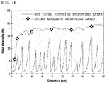
- FIG. 4 is a graph measuring peel strength of the metal pattern film according to one embodiment of the present application. Specifically, ITO was used as the adhesion promoting layer as in Example 1, and FIG. 4 is a graph measuring peel strength obtained therefrom. It was identified that the graph shape was more gradual compared to when the adhesion promoting layer was not used, which indicates no occurrences of stick/slip phenomenon, and it was identified that, through the strength of peel strength, adhesiveness also increased.
- a cross-cut test was used as a method of simply measuring adhesiveness between the substrate and the thin film formed on the substrate. This is a method of evaluating adhesiveness between substrates by forming 100 cells through making cuts 10 times vertically and horizontally at 1 mm intervals, and checking how much remains on the substrate when attaching and removing an adhesive tape (generally using ichiban tape) on the thin film.
Landscapes
- Chemical & Material Sciences (AREA)
- Organic Chemistry (AREA)
- Engineering & Computer Science (AREA)
- Mechanical Engineering (AREA)
- Chemical Kinetics & Catalysis (AREA)
- Materials Engineering (AREA)
- Metallurgy (AREA)
- General Chemical & Material Sciences (AREA)
- Health & Medical Sciences (AREA)
- Toxicology (AREA)
- Ceramic Engineering (AREA)
- Laminated Bodies (AREA)
Abstract
Description
- The present application claims priority to and the benefits of Korean Patent Application No.
10-2017-0072675 - The present application provides a metal pattern film comprising an adhesion promoting layer and a method for preparing the same.
- When manufacturing functional laminated glass used for automobiles or construction, polyvinyl butyral (PVB) is generally used as an adhesive. Laminated glass provided with special function is manufactured using a thermocompression process by inserting a polyvinyl butyral (PVB)-laminated functional film between two sheets of glass.
- In order to manufacture film-inserted functional laminated glass, adhesive strength between the polyvinyl butyral (PVB) and the functional film needs to be at a certain level or higher, and peel-off needs to be possible in order to allow reprocessing.
- When peeling off an existing polyvinyl butyral (PVB)-laminated polyvinyl butyral (PVB)/functional film, a stick-slip phenomenon occurs, which leads to a disadvantage such that wrinkles and stains remain making reuse impossible.
- A PET film is used as a functional film generally used in the art, and the PET film goes through a stick-slip phenomenon in the peel-off accompanying vibrations when peeling off between surfaces, and reuse is impossible since wrinkles and stains remain. Accordingly, in manufacturing functional laminated glass, a metal pattern film resolving a stick-slip phenomenon and thereby making reprocessing possible with no wrinkles and stains remaining.
- The present application is directed to providing a metal pattern film enhancing adhesive strength with an adhesive layer and resolving a stick-slip phenomenon when peeled off by forming an ultra-thin adhesion promoting layer on a surface of a substrate.
- One embodiment of the present application provides a metal pattern film comprising a substrate; a first adhesion promoting layer and a second adhesion promoting layer each provided on both surfaces of the substrate; a metal pattern provided on a surface opposite to the surface adjoining the substrate of the first adhesion promoting layer; a first adhesive layer provided on the surface provided with the metal pattern of the first adhesion promoting layer so as to cover the metal pattern; and a second adhesive layer provided on a surface opposite to the surface adjoining the substrate of the second adhesion promoting layer, wherein the first adhesion promoting layer and the second adhesion promoting layer comprise an inorganic oxide.
- Another embodiment of the present application provides laminated glass comprising the metal pattern film according to one embodiment of the present application.
- Still another embodiment of the present application provides a method for preparing a metal pattern film comprising preparing a substrate; forming a first adhesion promoting layer and a second adhesion promoting layer each on both surfaces of the substrate; forming a metal pattern on a surface opposite to the surface adjoining the substrate of the first adhesion promoting layer by patterning the metal pattern; forming a first adhesive layer on the surface provided with the metal pattern of the first adhesion promoting layer so as to cover the metal pattern; and forming a second adhesive layer on a surface opposite to the surface adjoining the substrate of the second adhesion promoting layer, wherein the first adhesion promoting layer and the second adhesion promoting layer comprise an inorganic oxide.
- A metal pattern film according to one embodiment of the present application forms an ultra-thin inorganic oxide layer on both surfaces of a substrate to enhance adhesive strength with an adhesive layer without decreasing transmittance, and by resolving a stick-slip phenomenon when peeled off, wrinkles and stain formation are prevented by reducing vibrations when peeling off between surfaces, which makes reprocessing possible.
- In addition, by forming an ultra-thin inorganic oxide layer, the metal pattern film according to one embodiment of the present application is effective in enhancing adhesiveness between a substrate and a pattern layer deposited on the substrate, and may comprise a function of an adhesion layer of a fabric of a metal mesh-based transparent conductive film.
- Furthermore, by using a nanoscale inorganic oxide layer, the metal pattern film according to one embodiment of the present application is transparent and has no changes in the optical properties of the film, and is thereby useful when manufacturing transparent functional laminated glass.
-
-
FIG. 1 is a side view illustrating a metal pattern film according to one embodiment of the present application. -
FIG. 2 is a diagram illustrating a peel-off process according to one embodiment of the present application. -
FIG. 3 is a diagram illustrating a method for preparing a metal pattern according to one embodiment of the present application. -
FIG. 4 is a diagram measuring peel strength of a metal pattern film according to one embodiment of the present application. -
- 10:
- Glass
- 20:
- First Adhesive Layer
- 30:
- Metal Pattern
- 40:
- First Adhesion Promoting Layer
- 50:
- Substrate
- 60:
- Second Adhesion Promoting Layer
- 70:
- Second Adhesive Layer
- 80:
- Glass
- 90:
- Metal Layer
- 100:
- Etching Resist Pattern
- Hereinafter, the present specification will be described in more detail.
- Embodiments of the present disclosure will be described in detail with reference to accompanying drawings so that those skilled in the art may readily implement the present disclosure. However, the present disclosure may be embodied in various different forms, and is not limited to the embodiments described herein.
- A metal pattern film according to one embodiment of the present application comprises a substrate; a first adhesion promoting layer and a second adhesion promoting layer each provided on both surfaces of the substrate; a metal pattern provided on a surface opposite to the surface adjoining the substrate of the first adhesion promoting layer; a first adhesive layer provided on the surface provided with the metal pattern of the first adhesion promoting layer so as to cover the metal pattern; and a second adhesive layer provided on a surface opposite to the surface adjoining the substrate of the second adhesion promoting layer, wherein the first adhesion promoting layer and the second adhesion promoting layer comprise an inorganic oxide.
- The metal pattern film according to one embodiment of the present application forms an ultra-thin inorganic oxide layer on both surfaces of a substrate to enhance adhesive strength with an adhesive layer without decreasing transmittance, and by resolving a stick-slip phenomenon when peeled off, wrinkles and stain formation are prevented by reducing vibrations when peeling off between surfaces, which makes reprocessing possible, and in addition thereto, is effective in enhancing adhesiveness between a pattern and the substrate by forming a nanoscale inorganic oxide layer.
- In the present specification, the stick-slip phenomenon means a friction phenomenon accompanying vibrations when peeling off between surfaces or a phenomenon decreasing precision through generating vibrations by causing a motion that is not smooth.
- In one embodiment of the present application, the substrate may be formed with a transparent polymer film.
- In one embodiment of the present application, the substrate may be formed with a PET film, a polycarbonate (PC) film, a polyethylene naphthalate (PEN) film, but is not limited thereto.
- In one embodiment of the present application, the substrate may have a thickness of greater than or equal to 1 µm and less than or equal to 200 µm, and preferably greater than or equal to 10 µm and less than or equal to 100 µm.
- In one embodiment of the present application, the first and the second adhesion promoting layers comprise one or more selected from the group consisting of niobium oxide (Nb2Ox), aluminum oxide (Al2O3), silicon oxide (SiO2), zinc oxide (ZnO), niobium oxide (NbO), tin oxide (SnO), zirconium oxide (ZrO) and indium tin oxide (ITO).
- In the niobium oxide (Nb2Ox), the range of x is an integer of 1 to 6, and preferably an integer of 1 to 4.
- In one embodiment of the present application, the first and the second adhesion promoting layers may be formed with aluminum oxide (Al2O3).
- In another embodiment, the first and the second adhesion promoting layers may be formed with silicon oxide (SiO2).
- In another embodiment, the first and the second adhesion promoting layers may be formed with indium tin oxide (ITO).
- In another embodiment, the Nb2Ox layer may be used alone as the first and the second adhesion promoting layers.
- When the Nb2Ox layer is used alone as the first and the second adhesion promoting layers, optical properties of the metal pattern film are most superior.
- In another embodiment, an alloy interlayer may be further included between the first adhesion promoting layer and the surface adjoining the substrate thereof.
- In another embodiment, an alloy interlayer may be further included between the second adhesion promoting layer and the surface adjoining the substrate thereof.
- In one embodiment of the present application, the alloy interlayer may have a thickness of greater than or equal to 0.5 nm and less than or equal to 1.9 nm, and preferably greater than or equal to 0.5 nm and less than or equal to 1.5 nm.
- The alloy interlayer having a thickness of 2 nm or greater leads to performance decline due to a decrease in the visible light transmittance.
- The alloy interlayer may be NiCr, Ni or Cr, but is not limited thereto.
- In the metal pattern film, when using an inorganic oxide layer as the first and the second adhesion promoting layers, a stick-slip phenomenon significantly decreases as a result of peel-off evaluation after thermocompressing the substrate (PET) and polyvinyl butyral (PVB), and as a result, wrinkles and stains do not remain making metal pattern film reprocessing possible.
- In one embodiment of the present application, the first and the second adhesion promoting layers each have a thickness of greater than or equal to 0.1 nm and less than or equal to 30 nm, preferably greater than or equal to 1 nm and less than or equal to 25 nm, and more preferably greater than or equal to 1 nm and less than or equal to 20 nm.
- Forming the adhesion promoting layer having a nanoscale thickness is useful in manufacturing transparent functional laminated glass since there are no changes in the optical properties of the film, and without decreasing transmittance, a stick-slip phenomenon may be resolved when peeled off as well as enhancing adhesive strength with an adhesive layer.
- The metal pattern film according to one embodiment of the present application has a metal pattern provided on a surface opposite to the surface adjoining the substrate of the first adhesion promoting layer.
- In one embodiment of the present application, the metal pattern may comprise one or more selected from the group consisting of aluminum, copper, nickel, chromium, gold, silver and platinum, and although copper having excellent electrical conductivity is most preferred as the metal pattern, the metal pattern is not limited thereto.
- In one embodiment of the present application, the metal pattern may have a line height of 10 µm or less and preferably 5 µm or less.
- The line height of the metal pattern means a distance from the surface adjoining the adhesion promoting layer to a surface opposite thereto.
- In one embodiment of the present application, the metal pattern may have a line height deviation of 20% or less and preferably 5% or less.
- The deviation means, based on an average line height, a percentage on a difference between the average line height and an individual line height.
- In one embodiment of the present application, the metal pattern may have a total aperture ratio, that is, a ratio of the substrate area that is not covered by the metal pattern, of 90% or greater, and preferably 95% or greater.
- In one embodiment of the present application, the metal pattern may have a line width of 40 µm or less, and specifically 0.1 µm to 40 µm or less.
- In one embodiment of the present application, the metal pattern has line-to-line spacing of 50 µm to 1000 µm.
- In one embodiment of the present application, the first and the second adhesive layers may comprise polyvinyl butyral (PVB), ethylene vinyl acetate (EVA), polyurethane (PU) or polyolefin (PO), and may preferably be a polyvinyl butyral (PVB) layer.
- In another embodiment, the first and the second adhesive layers may each have a thickness of greater than or equal to 1 µm and less than or equal to 1000 µm, and preferably greater than or equal to 1 µm and less than or equal to 760 µm.
- When each of the first and the second adhesive layers has the above-mentioned thickness, adhesiveness of the metal pattern film is enhanced, and particularly when further comprising laminated glass, an effect of preventing scattering of debris when the glass breaks down is obtained.
- One embodiment of the present application provides laminated glass comprising the metal pattern film.
- In one embodiment of the present application, the laminated glass is formed with a constitution further comprising glass on each of a surface opposite to the surface adjoining the pattern-formed first adhesion promoting layer of the first adhesive layer and a surface opposite to the surface adjoining the second adhesion promoting layer of the second adhesive layer.
- The laminated glass may be manufactured through thermocompressing the temporarily laminated adhesive layer of the metal pattern film and the glass.
- In one embodiment of the present application, as for the lamination of the first and the second adhesive layers and the glass, the temporarily laminated adhesive layer is inserted between tempered glass to manufacture into a sheet unit at a temperature of 140°C or higher using a thermocompression equipment such as a vacuum laminator or autoclave.
- According to one embodiment of the present application, a primer layer may be further provided at an interface of the metal pattern and the substrate.
- One embodiment of the present application provides a method for preparing a metal pattern film comprising preparing a substrate; forming a first adhesion promoting layer and a second adhesion promoting layer each on both surfaces of the substrate; forming a metal pattern on a surface opposite to the surface adjoining the substrate of the first adhesion promoting layer by patterning the metal pattern; forming a first adhesive layer on the surface provided with the metal pattern of the first adhesion promoting layer so as to cover the metal pattern; and forming a second adhesive layer on a surface opposite to the surface adjoining the substrate of the second adhesion promoting layer, wherein the first adhesion promoting layer and the second adhesion promoting layer comprise an inorganic oxide.
- In the preparation method according to one embodiment of the present application, the first and the second adhesion promoting layers may be formed on the substrate by a vapor deposition process using e-beam sputter equipment, however, the method is not limited thereto.
- In the preparation method according to one embodiment of the present application, the forming of first and second adhesive layers on each of the first adhesion promoting layer and the second adhesion promoting layer may use a process of thermocompression, solid-state adhesive film lamination or liquid-state adhesive solution coating, and preferably, a thermocompression process may be used.
- Pressure, temperature and time of the thermocompression process vary depending on the type of the adhesive layer used, however, the thermocompression process may be carried out at a temperature selected from a range of, for example, 60°C to 150°C, and a pressure may be applied as necessary.
- In one embodiment of the present application, the temporary lamination of the first and the second adhesive layers on both surfaces of the adhesion promoting layer may use a roll laminator at a temperature of approximately 80°C.
- In the preparation method according to one embodiment of the present application, the forming of a metal pattern comprises forming a metal layer; and forming a metal pattern by patterning the metal layer in the provided method for preparing a metal pattern film.
- In the preparation method according to one embodiment of the present application, the forming of a metal layer may be carried out through deposition or plating.
- In the preparation method according to one embodiment of the present application, the forming of a metal pattern by patterning the metal layer is carried out by, after forming an etching resist pattern on the metal layer, removing the metal layer that is not covered by the etching resist pattern in the provided method for preparing a metal pattern film.
- The forming of an etching resist pattern on the metal layer may use a photo process or a printing process, but is not limited thereto.
- After forming a metal pattern by selectively etching the etching resist pattern-formed metal layer in the preparation method according to one embodiment of the present application, removing the etching resist remaining on the top of the metal pattern using a peeling liquid may be further included.
- As the peeling liquid for removing the etching resist, an alkali solution or an organic solvent may be used.
- As the alkali solution, an aqueous sodium hydroxide solution diluted to a concentration of 1.0 wt% or greater, or potassium hydroxide may be used, and the alkali solution is not limited thereto as long as it is an alkali solution.
- As the organic solvent, ethanol, isopropyl alcohol or acetone may be used, and the organic solvent is not limited thereto as long as it is an organic solvent.
-
FIG. 3 is a diagram illustrating a process of forming a metal pattern on the adhesion promoting layer-formed substrate. Specifically, it is a diagram illustrating a process of forming a metal pattern by, after forming first and second adhesion promoting layers on a substrate and then forming a metal layer on the first adhesion promoting layer, forming an etching resist pattern and then selectively etching the result. - In the preparation method according to one embodiment of the present application, a method for preparing a metal pattern film further comprising a process of peeling the first adhesive layer from the metal pattern-provided substrate is provided.
-
FIG. 2 illustrates a peel-off process of the metal pattern film according to the present disclosure. Specifically, it is a process of peeling the first and the second adhesive layers from the metal pattern-provided substrate, and illustrates a process of peeling off the adhesive layer and the pattern film using physical force. - When laminating the first adhesive layer on the substrate, defects such as bubble generation, alien substance introduction or substrate wrinkling may occur, and the peel-off process may be progressed in order to reuse the first adhesive layer or the metal pattern-provided substrate, and herein, by using the first and the second adhesion promoting layers, advantages of resources recycling and production cost reduction are obtained by preventing a stick-slip phenomenon and thereby preventing damages on the first adhesive layer and the metal pattern substrate.
- By using the adhesion promoting layer according to one embodiment of the present application in the process of peeling off the first adhesive layer and the metal pattern-provided substrate, a metal pattern film with a significantly reduced stick-slip phenomenon may be prepared.
-
FIG. 1 illustrates a lamination structure of the metal pattern film. A method of forming a conductive heating pattern on a substrate and forming an adhesive layer has been used in the art, however, according to the present disclosure, a stick-slip phenomenon may be significantly reduced by further comprising an adhesion promoting layer on a substrate. - Hereinafter, examples of the present disclosure will be described in detail so that those skilled in the art may readily implement the present disclosure. However, the present disclosure may be embodied in various different forms, and is not limited to the examples described herein.
- Examples and comparative examples of a metal pattern film according to one embodiment of the present disclosure are described in the following Table 1.
- On polyethylene terephthalate (PET) having a thickness of 50 µm, 16 nm ITO was deposited on the PET as an adhesion promoting layer through a vapor deposition process using e-beam sputter equipment. After that, a Cu layer was formed on the ITO layer through plating, and then an etching resist pattern was formed through a printing process. After forming a metal pattern by selectively etching the etching resist pattern-formed metal layer, the etching resist remaining on the top of the metal pattern was removed using an aqueous sodium hydroxide solution with a concentration of 1.0 wt%. After that, PVB was laminated as an adhesive layer for 30 minutes under vacuum at 140°C to prepare a metal pattern film.
- Metal pattern films of Examples 2 to 4 were prepared in the same manner as in Example 1 except that materials of the following Table 1 were each used as the adhesion promoting layer.
- Metal pattern films of Comparative Examples 1 to 13 were prepared in the same manner as in Example 1 except that PET films supplied from film manufacturers described in the following Table 1 were each used instead of polyethylene terephthalate (PET), and the adhesion promoting layer was not used. The substrates of the following Table 1 are grade names of PET films supplied from various film manufacturers.
[Table 1] PET Manufacturer (Grade Name) Adhesion Promoting Layer (nm) Thickness (µm) Avg. 90 Peel Strength (N/cm) Max. 90 Peel Strength (N/cm) Stick/Slip Example 1 Toray (XG7PH2) ITO (16) 50 15.30 >20 X Example 2 Toray (XG7PH2) SiO2 (12) 50 >20 >20 X Example 3 Toray (XG7PH2) Al2O3 (8) 50 17.95 >20 X Example 4 Toray (XG7PH2) NbOx (5) 50 >20 >20 X Comparative Example 1 SKC (TH34) X 20 2.45 7.1 O Comparative Example 2 Teijin DuPont (KEL86W) X 50 0.80 2.87 O Comparative Example 3 Teijin DuPont (HPE) X 38 0.25 0.53 O Comparative Example 4 Teijin DuPont (G2P2) X 38 0.16 0.25 O Comparative Example 5 Teijin DuPont (G2PZ) X 38 1.30 5.36 O Comparative Example 6 Mitsubishi (O300E188W53B2) X 188 0.95 11.8 O Comparative Example 7 Mitsubishi (T604E50E92) X 50 0.58 3.6 O Comparative Example 8 Mitsubishi (T604E50M12) X 50 2.30 6.8 O Comparative Example 9 Toray (XD592) X 75 3.79 18.0 O Comparative Example 10 Toray (U48) X 50 2.62 13.0 O Comparative Example 11 Toray (XG7PH2) X 50 4.15 15.41 O Comparative Example 12 LGC Primer Coating PET (Front Surface) X 50 4.07 15.04 O Comparative Example 13 LGC Primer Coating PET (Rear Surface) X 50 1.90 5.27 O - In Table 1, it was identified that, depending on the presence of the adhesion promoting layer according to the present disclosure, Examples 1 to 4 thermocompressing inorganic oxide-deposited PET and PVB had no stick/slip phenomenon compared to Comparative Examples 1 to 13 without inorganic oxide layer deposition based on the peel-off evaluation results.
- The occurring of stick/slip phenomenon is determined from visual observation and the shape of a peel strength-measuring graph.
- In the method for measuring peel strength between the substrates in Table 1, average force according to a 90 degree peel strength test, a method measuring force for peeling off at a constant rate while maintaining an adhered surface and a peeled surface to be vertical, was expressed as Avg. 90 peel strength (N/cm), and the maximum value was expressed as Max. 90 peel strength (N/cm). The measurement values of the peel strength test are data capable of identifying adhesiveness between the substrate and the first adhesive layer and an effect of preventing a stick/slip phenomenon, and a texture analyzer (TA XT Plus) was used as a measuring device.
- In Table 1, it was identified that, in Examples 1 to 4, average force and maximum values for peeling off the first adhesive layer from the metal pattern-provided substrate all increased compared to Comparative Examples 1 to 13 without inorganic oxide layer deposition.
- Through such values, it was identified that, by using the adhesion promoting layer of the present disclosure, adhesiveness between the first adhesive layer and the substrate increased.
-
FIG. 4 is a graph measuring peel strength of the metal pattern film according to one embodiment of the present application. Specifically, ITO was used as the adhesion promoting layer as in Example 1, andFIG. 4 is a graph measuring peel strength obtained therefrom. It was identified that the graph shape was more gradual compared to when the adhesion promoting layer was not used, which indicates no occurrences of stick/slip phenomenon, and it was identified that, through the strength of peel strength, adhesiveness also increased. - From the following Table 2, damages on the metal pattern film when using various types of acids on the metal pattern film of the present disclosure may be identified when using NbOx (5 nm)/PET (100 µm) as the adhesion promoting layer and the adhesive layer of the metal pattern film. As seen from the following Table 2, it was identified that various types of acids caused no damages on the NbOx layer and a stick/slip phenomenon still did not occur.
[Table 2] Avg. 90 Peel Strength (N/cm) Max. 90 Peel Strength (N/cm) Stick/Slip Chemical Treatment X >20 >20 X Blending acid of phosphoric acid, Nitric acid and Acetic acid >20 >20 X Sulfuric Acid Hydrogen Peroxide >20 >20 X Iron Chloride >20 >20 X Client Company PET 6.12 7.13 X - In the following Table 3, it was identified that, although adhesive strength between a metal layer and a substrate is generally maintained by forming 20 nm or more of NiCr at the bottom of the metal layer since adhesive strength between metal layer-substrate decreases when electroplating on a metal seed film formed without an adhesion promoting layer due to an increase in the cohesiveness of the metal layer, adhesive strength between metal layer-substrate increased after plating when introducing an adhesion promoting layer such as NbOx, and particularly, optical properties were most superior when using Nb2Ox alone.
- A cross-cut test was used as a method of simply measuring adhesiveness between the substrate and the thin film formed on the substrate. This is a method of evaluating adhesiveness between substrates by forming 100 cells through making
cuts 10 times vertically and horizontally at 1 mm intervals, and checking how much remains on the substrate when attaching and removing an adhesive tape (generally using ichiban tape) on the thin film. - 95% to 100% of the thin film remaining based on the measurement is expressed as 5 B, and as the degree of maintaining the thin film on the substrate decreases, the expressed number decreases (4 B to 0 B), and this means adhesiveness decreasing. In the following Table 3, it was described as OK (5B) for the results checked as approximately 5 B in the cross-cut test between the plated metal layer and the substrate.
- As seen from the following Table 3, it was identified that adhesive strength between metal layer-film was not favorable (NG) after plating when an interlayer was not used, and adhesive strength between film-PVB was not favorable (NG) as well after removing the plating layer. It was identified that adhesive strength was improved when using an inorganic oxide interlayer, an alloy interlayer and an alloy+inorganic oxide interlayer.
- In the following Table 3, sheet resistance was measured using a contact-type sheet resistance measuring device (4-point probe), and transmittance was measured using a COH-400 transmittance measuring device (D65/10).
[Table 3] Category Interlayer Use X Inorganic Oxide Interlayer Alloy Interlayer Alloy+Inorganic Oxide Interlayer Metal Deposited Film Structure PET/Cu PET/Nb2Ox /Cu PET/NiCr/ Cu PET/NiCr/N b2Ox/Cu Before Plating Sheet Resistance (Ω/□) 0.2 0.2 0.2 0.2 Adhesive Strength between Metal Layer-Film OK (5B) OK (5B) OK (5B) OK (5B) After Plating Sheet Resistance (Ω/□) 0.01 0.01 0.01 0.01 Adhesive Strength between Metal Layer-Film NG OK (5B) OK (5B) OK (5B) After Transmittance (%) 90.01 88.37 86.82 83.75 Removing Plating Layer Scattering Degree (%) 1.09 1.55 1.12 1.21 Film-PVB Adhesive Strength (90 Degree Peel Test) NG (∼4 N/cm) OK (>20 N/cm) OK (∼15 N/cm) OK (>20 N/cm)
Claims (14)
- A metal pattern film comprising:a substrate;a first adhesion promoting layer and a second adhesion promoting layer each provided on both surfaces of the substrate;a metal pattern provided on a surface opposite to the surface adjoining the substrate of the first adhesion promoting layer;a first adhesive layer provided on the surface provided with the metal pattern of the first adhesion promoting layer so as to cover the metal pattern; anda second adhesive layer provided on a surface opposite to the surface adjoining the substrate of the second adhesion promoting layer,wherein the first adhesion promoting layer and the second adhesion promoting layer comprise an inorganic oxide.
- The metal pattern film of Claim 1, wherein the first and the second adhesion promoting layers comprise one or more selected from the group consisting of niobium oxide, aluminum oxide, silicon oxide, zinc oxide, niobium oxide, tin oxide, zirconium oxide and indium tin oxide.
- The metal pattern film of Claim 1, wherein the first and the second adhesion promoting layers each have a thickness of greater than or equal to 0.1 nm and less than or equal to 30 nm.
- The metal pattern film of Claim 1, wherein the metal pattern comprises one or more selected from the group consisting of aluminum, copper, nickel, chromium, gold, silver and platinum.
- The metal pattern film of Claim 1, wherein the metal pattern has a line height of 10 µm or less.
- The metal pattern film of Claim 1, wherein the metal pattern has a line height deviation of 20% or less.
- The metal pattern film of Claim 1, wherein the first and the second adhesive layers comprise polyvinyl butyral (PVB), ethylene vinyl acetate (EVA), polyurethane (PU) or polyolefin (PO) .
- The metal pattern film of Claim 1, wherein the first and the second adhesive layers are a polyvinyl butyral (PVB) layer.
- The metal pattern film of Claim 1, wherein the first and the second adhesive layers each have a thickness of greater than or equal to 1 µm and less than or equal to 1000 µm.
- Laminated glass comprising the metal pattern film of any one of Claims 1 to 9.
- A method for preparing the metal pattern film of any one of Claims 1 to 9, the method comprising:preparing a substrate;forming a first adhesion promoting layer and a second adhesion promoting layer each on both surfaces of the substrate;forming a metal pattern on a surface opposite to the surface adjoining the substrate of the first adhesion promoting layer by patterning the metal pattern;forming a first adhesive layer on the surface provided with the metal pattern of the first adhesion promoting layer so as to cover the metal pattern; andforming a second adhesive layer on a surface opposite to the surface adjoining the substrate of the second adhesion promoting layer,wherein the first adhesion promoting layer and the second adhesion promoting layer comprise an inorganic oxide.
- The method for preparing the metal pattern film of Claim 11, wherein the forming of a metal pattern comprises forming a metal layer; and forming a metal pattern by patterning the metal layer.
- The method for preparing the metal pattern film of Claim 12, wherein the forming of a metal pattern by patterning the metal layer is carried out by forming an etching resist pattern on the metal layer, and then removing the metal layer that is not covered by the etching resist pattern.
- The method for preparing the metal pattern film of Claim 11, further comprising peeling off the first adhesive layer from the metal pattern-provided substrate.
Applications Claiming Priority (2)
| Application Number | Priority Date | Filing Date | Title |
|---|---|---|---|
| KR1020170072675A KR102078438B1 (en) | 2017-06-09 | 2017-06-09 | Metal patterning film and method of preparing the same |
| PCT/KR2018/003607 WO2018225938A1 (en) | 2017-06-09 | 2018-03-27 | Metal pattern film and manufacturing method therefor |
Publications (3)
| Publication Number | Publication Date |
|---|---|
| EP3636430A1 true EP3636430A1 (en) | 2020-04-15 |
| EP3636430A4 EP3636430A4 (en) | 2020-04-29 |
| EP3636430B1 EP3636430B1 (en) | 2026-01-21 |
Family
ID=64566509
Family Applications (1)
| Application Number | Title | Priority Date | Filing Date |
|---|---|---|---|
| EP18812838.3A Active EP3636430B1 (en) | 2017-06-09 | 2018-03-27 | Metal pattern film and manufacturing method therefor |
Country Status (6)
| Country | Link |
|---|---|
| US (1) | US11090910B2 (en) |
| EP (1) | EP3636430B1 (en) |
| JP (1) | JP6930698B2 (en) |
| KR (1) | KR102078438B1 (en) |
| CN (1) | CN110719842B (en) |
| WO (1) | WO2018225938A1 (en) |
Families Citing this family (6)
| Publication number | Priority date | Publication date | Assignee | Title |
|---|---|---|---|---|
| KR102385925B1 (en) | 2018-11-05 | 2022-04-11 | 주식회사 엘지에너지솔루션 | Separator for electrochemical device and electrochemical device containing the same |
| WO2020198495A1 (en) | 2019-03-28 | 2020-10-01 | Vitro Flat Glass Llc | Coating for a heads-up display with low visible light reflectance |
| US20200369005A1 (en) * | 2019-05-23 | 2020-11-26 | Saint-Gobain Performance Plastics Corporation | Solar control film |
| WO2021163314A1 (en) | 2020-02-14 | 2021-08-19 | Vitro Flat Glass Llc | Low sheet resistance coating |
| KR102838164B1 (en) | 2022-06-09 | 2025-07-24 | 에스케이이노베이션 주식회사 | A separator, a manufacturing method thereof and an electrochemical device including the separator |
| CN115474302A (en) * | 2022-10-14 | 2022-12-13 | 广东省载诚新材料有限公司 | Glass heating membrane manufacturing method, glass heating membrane and device |
Family Cites Families (27)
| Publication number | Priority date | Publication date | Assignee | Title |
|---|---|---|---|---|
| JP2002348151A (en) * | 2001-05-25 | 2002-12-04 | Nippon Sheet Glass Co Ltd | Heat ray reflecting laminated windsheld glass |
| JP4203237B2 (en) * | 2001-11-15 | 2008-12-24 | 三菱樹脂株式会社 | Transparent gas barrier film laminate and transparent laminate |
| US7838102B2 (en) | 2004-10-28 | 2010-11-23 | E. I. Du Pont De Nemours And Company | Filled polyvinyl butyral sheeting for decorative laminated glass and a process for making same |
| JP4946584B2 (en) | 2007-04-12 | 2012-06-06 | 凸版印刷株式会社 | Metal pattern member |
| JP5401132B2 (en) | 2009-01-20 | 2014-01-29 | 信越ポリマー株式会社 | Radio wave transmitting decorative member and manufacturing method thereof |
| JP5120661B2 (en) | 2009-03-26 | 2013-01-16 | 住友金属鉱山株式会社 | Laminated structure |
| JP2012126578A (en) | 2009-04-13 | 2012-07-05 | Asahi Glass Co Ltd | Laminate for automobile glass, method for producing the same, and windshield |
| WO2011017039A2 (en) * | 2009-08-03 | 2011-02-10 | 3M Innovative Properties Company | Antireflective transparent emi shielding optical filter |
| JP5585143B2 (en) * | 2010-03-18 | 2014-09-10 | 凸版印刷株式会社 | Transparent conductive laminate, method for producing the same, and touch panel |
| KR20120012568A (en) | 2010-08-02 | 2012-02-10 | 송원호 | Probe plate with glass film, Probe plate with glass film formed |
| JP5822132B2 (en) * | 2011-12-16 | 2015-11-24 | 大日本印刷株式会社 | LAMINATE AND CONDUCTIVE PATTERN FILM MANUFACTURING METHOD |
| KR101707042B1 (en) * | 2013-06-19 | 2017-02-17 | 일진머티리얼즈 주식회사 | Conducting heart dissipating sheet, electric component and electronics device comprising the sheet |
| JP6295551B2 (en) * | 2013-09-03 | 2018-03-20 | 凸版印刷株式会社 | Transparent conductive laminate, touch panel, and method for producing transparent conductive laminate |
| WO2015080482A1 (en) | 2013-11-29 | 2015-06-04 | 주식회사 엘지화학 | Heating element and method for manufacturing same |
| KR101549987B1 (en) | 2013-12-23 | 2015-09-03 | (주)창성 | A composite film using conductive adhesion layers, having improved heat sink capabilities with graphite layer and method of fabricating the same. |
| WO2015109198A1 (en) | 2014-01-17 | 2015-07-23 | Pleotint, L.L.C. | Reflective and conductive coatings directly on pvb |
| JP6379771B2 (en) | 2014-07-14 | 2018-08-29 | 大日本印刷株式会社 | Laminated glass, mesh sheet and intermediate member for laminated glass |
| US9128663B1 (en) * | 2014-08-04 | 2015-09-08 | T-Kingdom Co., Ltd. | Touch sensing electrode structure and method of manufacturing same |
| JP6295885B2 (en) * | 2014-08-21 | 2018-03-20 | 大日本印刷株式会社 | Laminated glass, vehicles and windows |
| JP2016102055A (en) | 2014-11-17 | 2016-06-02 | 大日本印刷株式会社 | Glass laminate, pattern sheet and manufacturing method of glass laminate |
| US10912155B2 (en) | 2014-11-17 | 2021-02-02 | Dai Nippon Printing Co., Ltd. | Heating plate, conductive pattern sheet, vehicle, and method of manufacturing heating plate |
| JP6492644B2 (en) | 2014-12-25 | 2019-04-03 | 大日本印刷株式会社 | Heating plate and vehicle |
| KR20160079296A (en) | 2014-12-26 | 2016-07-06 | 주식회사 엘지화학 | Photocurable pigment dispersion liquid and photocurable ink composition using the same |
| KR20150116767A (en) | 2015-01-06 | 2015-10-16 | 존스미디어 주식회사 | Windowpane with decorative film |
| JP6060223B1 (en) * | 2015-07-22 | 2017-01-11 | 日東電工株式会社 | Cover member having a transparent adhesive layer |
| KR102564346B1 (en) | 2015-12-17 | 2023-08-08 | 엘지전자 주식회사 | Display device |
| KR101718780B1 (en) | 2016-06-24 | 2017-03-24 | 현대안전유리공업(주) | Laminated glass and method for manufacturing the same |
-
2017
- 2017-06-09 KR KR1020170072675A patent/KR102078438B1/en active Active
-
2018
- 2018-03-27 JP JP2019566944A patent/JP6930698B2/en active Active
- 2018-03-27 WO PCT/KR2018/003607 patent/WO2018225938A1/en not_active Ceased
- 2018-03-27 EP EP18812838.3A patent/EP3636430B1/en active Active
- 2018-03-27 CN CN201880036896.5A patent/CN110719842B/en active Active
- 2018-03-27 US US16/619,763 patent/US11090910B2/en active Active
Also Published As
| Publication number | Publication date |
|---|---|
| US20200101700A1 (en) | 2020-04-02 |
| EP3636430B1 (en) | 2026-01-21 |
| JP2020522407A (en) | 2020-07-30 |
| KR102078438B1 (en) | 2020-02-17 |
| WO2018225938A1 (en) | 2018-12-13 |
| CN110719842B (en) | 2021-08-24 |
| JP6930698B2 (en) | 2021-09-01 |
| US11090910B2 (en) | 2021-08-17 |
| EP3636430A4 (en) | 2020-04-29 |
| KR20180134654A (en) | 2018-12-19 |
| CN110719842A (en) | 2020-01-21 |
Similar Documents
| Publication | Publication Date | Title |
|---|---|---|
| EP3636430B1 (en) | Metal pattern film and manufacturing method therefor | |
| EP2722853B1 (en) | Conductive laminate, transparent conductive laminate with patterned wiring, and optical device | |
| JP5932098B2 (en) | Transparent conductive film | |
| US20220256694A1 (en) | Display device including formable transparent conductive films with metal nanowires | |
| CN109074906B (en) | Light-transmitting film | |
| EP3381882A1 (en) | Interlayer for laminated glass, and laminated glass | |
| KR102367519B1 (en) | light transmissive film | |
| JP2012054006A (en) | Transparent conductive gas barrier film and method for producing the same | |
| JP5781428B2 (en) | Conductive film and conductive film roll | |
| KR102667935B1 (en) | Conductive film and touch panel | |
| KR102530121B1 (en) | Transparent conductive film | |
| KR20180012731A (en) | Transparent conductive film | |
| US11812524B2 (en) | Heating film and method for manufacturing same | |
| EP3306448A1 (en) | Interlayer filler material for touch panels, and laminate | |
| EP3690542A1 (en) | Electrochromic dimming member, light-transmitting conductive glass film and electrochromic dimming element | |
| CN107578840B (en) | Transparent conductors and touch screens | |
| KR102032011B1 (en) | Conductive laminate and transparent electrode comprising thereof | |
| TWI706299B (en) | Conductive substrate, manufacturing method of conductive substrate | |
| US20200163164A1 (en) | Heater member, heater tape, and molded body equipped with heater member | |
| JP6144798B2 (en) | Transparent conductive film | |
| KR20200063976A (en) | Transparent conductive film, and patterning method thereof | |
| JP2613206B2 (en) | Method for producing transparent conductive film | |
| JP2016177820A (en) | Transparent conductive film | |
| JP2018170360A (en) | Conductive film, electrode, electronic apparatus, electrostatic capacitance type input device, and manufacturing method of electrode | |
| TW201528891A (en) | Method of forming a conductive path comprising silver and a composite comprising the same |
Legal Events
| Date | Code | Title | Description |
|---|---|---|---|
| STAA | Information on the status of an ep patent application or granted ep patent |
Free format text: STATUS: THE INTERNATIONAL PUBLICATION HAS BEEN MADE |
|
| PUAI | Public reference made under article 153(3) epc to a published international application that has entered the european phase |
Free format text: ORIGINAL CODE: 0009012 |
|
| STAA | Information on the status of an ep patent application or granted ep patent |
Free format text: STATUS: REQUEST FOR EXAMINATION WAS MADE |
|
| 17P | Request for examination filed |
Effective date: 20191129 |
|
| AK | Designated contracting states |
Kind code of ref document: A1 Designated state(s): AL AT BE BG CH CY CZ DE DK EE ES FI FR GB GR HR HU IE IS IT LI LT LU LV MC MK MT NL NO PL PT RO RS SE SI SK SM TR |
|
| AX | Request for extension of the european patent |
Extension state: BA ME |
|
| A4 | Supplementary search report drawn up and despatched |
Effective date: 20200330 |
|
| RIC1 | Information provided on ipc code assigned before grant |
Ipc: C23F 1/02 20060101ALI20200324BHEP Ipc: B32B 17/10 20060101ALI20200324BHEP Ipc: C09J 129/04 20060101ALI20200324BHEP Ipc: C23C 14/08 20060101ALI20200324BHEP Ipc: B32B 9/04 20060101AFI20200324BHEP Ipc: B32B 38/10 20060101ALI20200324BHEP Ipc: B32B 17/06 20060101ALI20200324BHEP Ipc: B32B 7/12 20060101ALI20200324BHEP |
|
| DAV | Request for validation of the european patent (deleted) | ||
| DAX | Request for extension of the european patent (deleted) | ||
| STAA | Information on the status of an ep patent application or granted ep patent |
Free format text: STATUS: EXAMINATION IS IN PROGRESS |
|
| 17Q | First examination report despatched |
Effective date: 20211001 |
|
| GRAP | Despatch of communication of intention to grant a patent |
Free format text: ORIGINAL CODE: EPIDOSNIGR1 |
|
| STAA | Information on the status of an ep patent application or granted ep patent |
Free format text: STATUS: GRANT OF PATENT IS INTENDED |
|
| INTG | Intention to grant announced |
Effective date: 20250919 |
|
| GRAS | Grant fee paid |
Free format text: ORIGINAL CODE: EPIDOSNIGR3 |
|
| GRAA | (expected) grant |
Free format text: ORIGINAL CODE: 0009210 |
|
| STAA | Information on the status of an ep patent application or granted ep patent |
Free format text: STATUS: THE PATENT HAS BEEN GRANTED |
|
| AK | Designated contracting states |
Kind code of ref document: B1 Designated state(s): AL AT BE BG CH CY CZ DE DK EE ES FI FR GB GR HR HU IE IS IT LI LT LU LV MC MK MT NL NO PL PT RO RS SE SI SK SM TR |
|
| REG | Reference to a national code |
Ref country code: CH Ref legal event code: F10 Free format text: ST27 STATUS EVENT CODE: U-0-0-F10-F00 (AS PROVIDED BY THE NATIONAL OFFICE) Effective date: 20260121 |
|
| REG | Reference to a national code |
Ref country code: DE Ref legal event code: R096 Ref document number: 602018088728 Country of ref document: DE |
|
| REG | Reference to a national code |
Ref country code: IE Ref legal event code: FG4D |
|
| PGFP | Annual fee paid to national office [announced via postgrant information from national office to epo] |
Ref country code: GB Payment date: 20260224 Year of fee payment: 9 |
|
| PGFP | Annual fee paid to national office [announced via postgrant information from national office to epo] |
Ref country code: DE Payment date: 20260220 Year of fee payment: 9 |
|
| PGFP | Annual fee paid to national office [announced via postgrant information from national office to epo] |
Ref country code: FR Payment date: 20260224 Year of fee payment: 9 |