EP3629393A1 - Oled device packaging assembly and packaging method, and display apparatus - Google Patents
Oled device packaging assembly and packaging method, and display apparatus Download PDFInfo
- Publication number
- EP3629393A1 EP3629393A1 EP17911303.0A EP17911303A EP3629393A1 EP 3629393 A1 EP3629393 A1 EP 3629393A1 EP 17911303 A EP17911303 A EP 17911303A EP 3629393 A1 EP3629393 A1 EP 3629393A1
- Authority
- EP
- European Patent Office
- Prior art keywords
- blocking layer
- oled device
- pattern region
- buffer layer
- heat
- Prior art date
- Legal status (The legal status is an assumption and is not a legal conclusion. Google has not performed a legal analysis and makes no representation as to the accuracy of the status listed.)
- Withdrawn
Links
Images


Classifications
-
- H—ELECTRICITY
- H10—SEMICONDUCTOR DEVICES; ELECTRIC SOLID-STATE DEVICES NOT OTHERWISE PROVIDED FOR
- H10K—ORGANIC ELECTRIC SOLID-STATE DEVICES
- H10K50/00—Organic light-emitting devices
- H10K50/80—Constructional details
- H10K50/84—Passivation; Containers; Encapsulations
- H10K50/844—Encapsulations
-
- H—ELECTRICITY
- H10—SEMICONDUCTOR DEVICES; ELECTRIC SOLID-STATE DEVICES NOT OTHERWISE PROVIDED FOR
- H10K—ORGANIC ELECTRIC SOLID-STATE DEVICES
- H10K50/00—Organic light-emitting devices
- H10K50/80—Constructional details
- H10K50/87—Arrangements for heating or cooling
-
- H—ELECTRICITY
- H10—SEMICONDUCTOR DEVICES; ELECTRIC SOLID-STATE DEVICES NOT OTHERWISE PROVIDED FOR
- H10K—ORGANIC ELECTRIC SOLID-STATE DEVICES
- H10K59/00—Integrated devices, or assemblies of multiple devices, comprising at least one organic light-emitting element covered by group H10K50/00
- H10K59/80—Constructional details
- H10K59/87—Passivation; Containers; Encapsulations
- H10K59/873—Encapsulations
-
- H—ELECTRICITY
- H10—SEMICONDUCTOR DEVICES; ELECTRIC SOLID-STATE DEVICES NOT OTHERWISE PROVIDED FOR
- H10K—ORGANIC ELECTRIC SOLID-STATE DEVICES
- H10K59/00—Integrated devices, or assemblies of multiple devices, comprising at least one organic light-emitting element covered by group H10K50/00
- H10K59/80—Constructional details
- H10K59/8794—Arrangements for heating and cooling
-
- H—ELECTRICITY
- H10—SEMICONDUCTOR DEVICES; ELECTRIC SOLID-STATE DEVICES NOT OTHERWISE PROVIDED FOR
- H10K—ORGANIC ELECTRIC SOLID-STATE DEVICES
- H10K71/00—Manufacture or treatment specially adapted for the organic devices covered by this subclass
-
- H—ELECTRICITY
- H10—SEMICONDUCTOR DEVICES; ELECTRIC SOLID-STATE DEVICES NOT OTHERWISE PROVIDED FOR
- H10K—ORGANIC ELECTRIC SOLID-STATE DEVICES
- H10K2102/00—Constructional details relating to the organic devices covered by this subclass
- H10K2102/301—Details of OLEDs
- H10K2102/311—Flexible OLED
-
- H—ELECTRICITY
- H10—SEMICONDUCTOR DEVICES; ELECTRIC SOLID-STATE DEVICES NOT OTHERWISE PROVIDED FOR
- H10K—ORGANIC ELECTRIC SOLID-STATE DEVICES
- H10K71/00—Manufacture or treatment specially adapted for the organic devices covered by this subclass
- H10K71/40—Thermal treatment, e.g. annealing in the presence of a solvent vapour
Definitions
- the present invention relates to display field, and more particularly, to a package component of an Organic Light Emitting Diode (OLED) device and a package method thereof, and a display device.
- OLED Organic Light Emitting Diode
- OLED Organic Light Emitting Diode
- LCD liquid crystal display
- An organic thin film is formed on a substrate and between cathode metal and anode metal. Forward voltage is applied to the two electrodes and the organic thin film emits light.
- Organic material of the organic thin film is sensitive to water vapor and oxygen so infiltrate of water and oxygen can reduce lifetime of the OLED device. For achieving requirement of lifetime and stabilization in market, quality of packaging OLED device is very high.
- a conventional method adopts thin film packaging to package the OLED device.
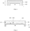
- a package thin film 12 is formed on the OLED device 11 and covers it.
- the package thin film 12 is formed by alternately depositing a blocking layer 121 and a buffer layer 122.
- the blocking layer 121 is effective blocking layer for oxygen and water.
- the main composition of the blocking layer 121 is inorganic material. Defect such as pinholes and particles can appear in the manufacturing process.
- the main composition of the buffer layer 122 is organic material to cover the defects of the blocking layer 121 and be flat. The stronger the ability blocking oxygen and water is, the thicker the blocking layer 121 is. The bigger the stress of the OLED device 11 is when bending, the easier peeling of the thin film 12 form the OLED device 11 is.
- the conventional method adopts Ink-jet printing (IJP) to form the buffer layer 122. How to prevent leakage of the buffer layer 122 is very important.
- the design of the OLED device becomes thin so the wiring is closer and how to improving heat dissipating of the OLED device is very important as well.
- the present invention provides a package component of an Organic Light Emitting Diode (OLED) device and a package method thereof, and a display device to avoid package thin film peeling because the OLED device is bending and to prevent drop leakage of adopting Ink-jet printing (IJP) to form package thin film. It can improve heat dissipation of the OLED device as well.
- OLED Organic Light Emitting Diode
- IJP Ink-jet printing
- An embodiment of the present invention provides a package component of an OLED device, including:
- An embodiment of the present invention provides a display device comprising a package component, the package component including:
- An embodiment of the present invention provides a method of packaging an OLED device, comprising:
- the first blocking layer includes a predetermined pattern so thickness of the first blocking layer at the first pattern region is smaller than that at the second pattern region. It reduces stress applied to the first blocking layer when the OLED device is bending. Moreover, the first pattern region can accommodate drops of forming the buffer layer via IJP to avoid leakage. The heat-dissipating particles in the buffer layer can improve heat dissipation of the OLED device.
- FIG. 2 is a cross-sectional view of a display device in accordance with an embodiment of the present invention.
- the display device includes an Organic Light Emitting Diode (OLED) device 20 and a package component of the OLED device 20.
- the package component can include substrate 21, a first blocking layer 22, and a buffer layer 23.
- the OLED device 20 is on the substrate 21.
- the substrate 21 includes but is not limited to transparent glass substrate and transparent plastic substrate.
- the substrate 21 can adopt transparent plastic substrate which is bendable.
- the first blocking layer 22 covers the OLED device 20.
- a side of the first blocking layer 22 far away from the OLED device 20 includes predetermined patterns, as FIG. 3 shown.
- the first blocking layer 22 can include multiple band areas which are set alternately along a direction horizontal to the substrate 21 (horizontal direction). Each band area includes a first pattern region 221 and a second pattern region 222 alternately set along vertical direction. Thickness of the first blocking layer 22 at the first pattern region 221 is smaller than that at the second pattern region 222.
- a third pattern region 223 is between two adjacent band areas and can expose a surface of the OLED device 20.
- the present invention can adopt Plasma Enhanced Chemical Vapor Deposition (PECVD) to form the first blocking layer 22.
- PECVD Plasma Enhanced Chemical Vapor Deposition
- the substrate 21 on which the OLED device 20 is located is set in a sealing chamber, and a mask 40 is set on the OLED device 20.
- the mask 40 includes a hollow region 41 and an non-hollow region 42.
- the hollow region 41 includes a first subregion 411 and a second subregion 412 which are connected with each other, and area of the first subregion 411 is less than that of the second subregion 412.
- the shapes of the first subregion 411 and the second subregion 412 can be rectangle.
- the shapes of the first subregion 411 and the second subregion 412 can be the same in top view. Reacting gas is passed into the sealing chamber.
- a mixing gas has SiH 4 , NH 3 , and N 2 .
- RF discharge is applied to the reacting gas so SiN x is generated by the reaction.
- SiN x passes the hollow region 41 of the mask 40 and is deposited on the OLED device 20 to form the first blocking layer 22.
- the mask 40 When number of the hollow region 41 of the mask 40 is less than that of the first pattern region 221 or the second pattern region 222, the mask 40 can be moved horizontally to a predetermined region and PECVD is performed again after one PECVD process. Distance and times of movement are determined according to design pattern and number of the first pattern region 221 and the second pattern region 222 of the first blocking layer 22. Thus, the first blocking layer 22 including the predetermined pattern is formed.
- the present invention can adopt one of Atomic Layer Deposition (ALD), Physical Vapor Deposition (PVD), and Chemical Vapor Deposition (CVD), and collaborate with the mask 40 to form the first blocking layer 22 having the predetermined pattern.
- ALD Atomic Layer Deposition
- PVD Physical Vapor Deposition
- CVD Chemical Vapor Deposition
- Material of the first blocking layer 22 can be other inorganic material such as aluminum nitride, aluminum oxide, aluminum nitrogen oxide, silicon oxide, or silicon nitrogen oxide.
- the buffer layer 23 is coated on the first blocking layer 22 and can fully cover the first pattern region 221, the second pattern region 222, and the third pattern region 223. That is, the buffer layer 23 can fully cover an entire structure of the first blocking layer 22. In another embodiment of the present invention, the buffer layer 23 can merely cover the first pattern region 221 and the third pattern region 223. In addition, the buffer layer 23 is doped with heat-dissipating particles 231.
- Material of the buffer layer 23 can be organic material such as epoxy, silicon polymer, or PMMA.
- Material of the heat-dissipating particles 231 can be material of high thermal conductivity coefficient such as graphene, Carbon Nanotube, Al 2 O 3 , MgO, ZnO, AlN, BN. It can also be Ag, Cu, Au, and alloy thereof.
- the present invention can form the buffer layer 23 without the mask. It can adopt one of One Drop Filling (ODF), JIP and Nozzle Printing to form the buffer layer 23 and save cost of mask design and production, for example. Cost of production and manufacturing entire package component can be reduced as well.
- ODF One Drop Filling
- JIP JIP
- Nozzle Printing to form the buffer layer 23 and save cost of mask design and production, for example. Cost of production and manufacturing entire package component can be reduced as well.
- ODF for example, provides hydrophilic modification to nano Al 2 O 3 particles and uniformly disperses the Al 2 O 3 particles in epoxy via high shear dispersing emulsifier.
- the doping amount of the Al 2 O 3 particles can be 3 ⁇ 50 wt% and viscosity of the buffer solution is less than 0.5Pa ⁇ s.
- the buffer solution is cured in 80 ⁇ 100°C to form the buffer layer 23.
- the present invention also can adopt UV curing to form the buffer layer 23.
- the first blocking layer 22 is effective blocking layer for water and oxygen.
- the buffer layer 23 can cover the first blocking layer 22 and perform flattening.
- the buffer layer 23 and the first blocking layer 22 can be deemed as package thin film of the OLED device 20.
- thickness of the first blocking layer 22 at the first pattern region 221 is smaller than that at the second pattern region 222 in the present invention. Namely, a side of the first blocking layer 22 far away from the OLED device 20 is patterned. The edges of the first pattern region 221 and the second pattern region 222 cannot be squeezed when the OLED device 20 is bending, and stress of the first blocking layer 22 is reduced. Thus it can avoid that the package thin film is peeled when the OLED device 20 is bending.
- the first pattern region 221 can accommodate drops of forming the buffer layer 23 via IJP to avoid leakage.
- the heat-dissipating particles 231 in the buffer layer 23 can improve heat dissipation of the OLED device 20.
- adding the heat-dissipating particles 231 into the buffer layer 23 can extend route of water and oxygen entering the OLED device 20 and improve the resistibility of water and oxygen.
- the present can adopt heat-dissipating material of high light transmittance to form the heat-dissipating particles 231 and ensure the light-output performance.
- the package component can further include a second blocking layer 24 covering the buffer layer 23 and the first blocking layer 22 in accordance with an embodiment of the present invention.
- Material of the second blocking layer 24 can be the same as that of the first blocking layer 22.
- the present invention can form the second blocking layer 24 without the mask.
- a method of forming the second blocking layer 24 can adopt one of ODF, Nozzle Imprinting, and Nozzle Printing to save cost, for example.
- a surface of the second blocking layer 24 far away from the buffer layer 23 can be a flat plane.
- a protective film or a touch sensor film of touch sensor function is attached to the flat plane. There is no small gully at the attaching part of the flat plane and the protective film or the touch sensor film to avoid bubble when the OLED device 20 displays.
- FIG. 5 is a flow chart of packaging an OLED device in accordance with an embodiment of the present invention.
- the packaging method can include the following steps S51 ⁇ S54.
- the substrate includes but is not limited to transparent glass substrate and transparent plastic substrate.
- the substrate can adopt transparent plastic substrate which is bendable.
- a side of the first blocking layer far away from the OLED device includes a first pattern region and a second pattern region alternately set along a predetermined direction. Thickness of the first blocking layer at the first pattern region is smaller than that at the second pattern region.
- the side of the first blocking layer far away from the OLED device includes predetermined patterns.
- the first blocking layer can include multiple band areas which are set alternately along a direction horizontal to the substrate (horizontal direction). Each band area includes the first pattern region and the second pattern region alternately set along vertical direction. Thickness of the first blocking layer at the first pattern region is smaller than that at the second pattern region.
- a third pattern region is between two adjacent band areas and can expose a surface of the OLED device.
- the present invention can adopt PECVD to form the first blocking layer.
- the substrate loading the OLED device is set in a sealing chamber, and a mask is located on the OLED device.
- the mask includes a hollow region and an non-hollow region.
- the hollow region includes a first subregion and a second subregion connected thereto, and area of the first subregion is less than that of the second subregion.
- the shapes of the first subregion and the second subregion can be rectangle.
- the shapes of the first subregion and the second subregion can be the same in top view.
- Reacting gas is passed into the sealing chamber.
- a mixing gas has SiH 4 , NH 3 , and N 2 .
- RF discharge is applied to the reacting gas so SiN x is generated by the reaction.
- SiN x passes the hollow region of the mask and is deposited on the OLED device to form the first blocking layer.
- the mask When number of the hollow region of the mask is less than that of the first pattern region or the second pattern region, the mask can be moved horizontally to a predetermined region and PECVD is performed again after one PECVD process. Distance and times of movement is determined according to designed pattern and number of the first pattern region and the second pattern region of the first blocking layer. Thus, the first blocking layer including the predetermined pattern is formed.
- the present invention can adopt one of ALD, PVD, and CVD, and collaborate with the mask to form the first blocking layer 22 having the predetermined pattern.
- Material of the first blocking layer can be other inorganic material such as aluminum nitride, aluminum oxide, aluminum nitrogen oxide, silicon oxide, or silicon nitrogen oxide.
- the buffer layer is doped with heat-dissipating particles.
- the buffer layer can fully cover the first pattern region, the second pattern region, and the third pattern region. That is, the buffer layer can fully cover an entire structure of the first blocking layer. In another embodiment of the present invention, the buffer layer can merely cover the first pattern region and the third pattern region. In addition, the buffer layer is doped with the heat-dissipating particles. Furthermore, the present can adopt heat-dissipating material of high light transmittance to form the heat-dissipating particles and ensure the light-output performance.
- Material of the buffer layer can be organic material such as epoxy, silicon polymer, or PMMA.
- Material of the heat-dissipating particles can be material of high thermal conductivity coefficient such as graphene, carbon nanotube, Al 2 O 3 , MgO, ZnO, AlN, BN. It can also be Ag, Cu, Au, and alloy thereof.
- the present invention can form the buffer layer without the mask. It can adopt one of ODF, Ink-jet printing (IJP), and Nozzle Printing to form the buffer layer and save cost of mask design and production. Cost of production and manufacturing entire package component can be reduced as well.
- IJP Ink-jet printing
- Nozzle Printing to form the buffer layer and save cost of mask design and production. Cost of production and manufacturing entire package component can be reduced as well.
- ODF for example, provides hydrophilic modification to nano Al 2 O 3 particles and uniformly disperses the Al 2 O 3 particles in epoxy via high shear dispersing emulsifier.
- the doping amount of the Al 2 O 3 particles can be 3 ⁇ 50 wt% and viscosity of the buffer solution is less than 0.5Pa ⁇ s.
- the buffer solution is cured in 80 ⁇ 100°C to form the buffer layer.
- the present invention also can adopt UV curing to form the buffer layer.
- the present invention can further form a second blocking layer covering the buffer layer and the first blocking layer. That is, the packaging method can further includes step S55.
- a surface of the second blocking layer far away from the buffer layer can be a flat plane.
- Material of the second blocking layer can be the same as that of the first blocking layer.
- the present invention can form the second blocking layer without the mask. It can adopt one of ODF, Ink-jet printing (IJP), and Nozzle Printing to form the buffer layer and save cost, for example.
- the method of packaging the OLED device above can be adopted to manufacture the package component shown in FIG. 2 .
Landscapes
- Physics & Mathematics (AREA)
- Optics & Photonics (AREA)
- Engineering & Computer Science (AREA)
- Manufacturing & Machinery (AREA)
- Electroluminescent Light Sources (AREA)
- Devices For Indicating Variable Information By Combining Individual Elements (AREA)
Abstract
Description
- The present invention relates to display field, and more particularly, to a package component of an Organic Light Emitting Diode (OLED) device and a package method thereof, and a display device.
- Organic Light Emitting Diode (OLED) is a new display device and difference between a conventional liquid crystal display (LCD) and it is that OLED does not need a backlight source. An organic thin film is formed on a substrate and between cathode metal and anode metal. Forward voltage is applied to the two electrodes and the organic thin film emits light. Organic material of the organic thin film is sensitive to water vapor and oxygen so infiltrate of water and oxygen can reduce lifetime of the OLED device. For achieving requirement of lifetime and stabilization in market, quality of packaging OLED device is very high.
- A conventional method adopts thin film packaging to package the OLED device. Referring
FIG. 1 , a packagethin film 12 is formed on theOLED device 11 and covers it. The packagethin film 12 is formed by alternately depositing ablocking layer 121 and abuffer layer 122. Theblocking layer 121 is effective blocking layer for oxygen and water. The main composition of theblocking layer 121 is inorganic material. Defect such as pinholes and particles can appear in the manufacturing process. The main composition of thebuffer layer 122 is organic material to cover the defects of theblocking layer 121 and be flat. The stronger the ability blocking oxygen and water is, the thicker theblocking layer 121 is. The bigger the stress of theOLED device 11 is when bending, the easier peeling of thethin film 12 form theOLED device 11 is. For improving the utilizing efficiency of material and saving cost, the conventional method adopts Ink-jet printing (IJP) to form thebuffer layer 122. How to prevent leakage of thebuffer layer 122 is very important. In addition, the design of the OLED device becomes thin so the wiring is closer and how to improving heat dissipating of the OLED device is very important as well. - The present invention provides a package component of an Organic Light Emitting Diode (OLED) device and a package method thereof, and a display device to avoid package thin film peeling because the OLED device is bending and to prevent drop leakage of adopting Ink-jet printing (IJP) to form package thin film. It can improve heat dissipation of the OLED device as well.
- An embodiment of the present invention provides a package component of an OLED device, including:
- a substrate, loading the OLED device;
- a first blocking layer covering the OLED device , a side of the first blocking layer far away from the OLED device including a first pattern region and a second pattern region alternately set along a predetermined direction, wherein thickness of the first blocking layer at the first pattern region is smaller than that at the second pattern region ; and
- a buffer layer coated on the first blocking layer, including heat-dissipating particles.
- An embodiment of the present invention provides a display device comprising a package component, the package component including:
- a substrate, loading the OLED device;
- a first blocking layer covering the OLED device , a side of the first blocking layer far away from the OLED device including a first pattern region and a second pattern region alternately set along a predetermined direction, wherein thickness of the first blocking layer at the first pattern region is smaller than that at the second pattern region; and
- a buffer layer coated on the first blocking layer, including heat-dissipating particles.
- An embodiment of the present invention provides a method of packaging an OLED device, comprising:
- providing a substrate;
- loading the OLED device on the substrate;
- covering the OLED device with a first blocking layer, wherein a side of the first blocking layer far away from the OLED device includes a first pattern region and a second pattern region alternately set along a predetermined direction, and thickness of the first blocking layer at the first pattern region is smaller than that at the second pattern region; and
- coating a buffer layer on the first blocking layer, the buffer layer including heat-dissipating particles.
- The benefit of the present invention is that the first blocking layer includes a predetermined pattern so thickness of the first blocking layer at the first pattern region is smaller than that at the second pattern region. It reduces stress applied to the first blocking layer when the OLED device is bending. Moreover, the first pattern region can accommodate drops of forming the buffer layer via IJP to avoid leakage. The heat-dissipating particles in the buffer layer can improve heat dissipation of the OLED device.
- The accompanying drawings are included to provide easy understanding of the application, are incorporated herein and constitute a part of this specification. The drawings illustrate embodiments of the application and, together with the description, serve to illustrate the principles of the application.
-
FIG. 1 is a cross-sectional view of a package component of a conventional OLED device. -
FIG. 2 is a cross-sectional view of a display device in accordance with an embodiment of the present invention. -
FIG. 3 is a top view of a structure of a buffer layer and a first blocking layer shown inFIG. 2 . -
FIG. 4 is a top view of a structure of a mask manufacturing the first blocking layer shown inFIG. 3 . -
FIG. 5 is a flow chart of manufacturing an OLED device in accordance with an embodiment of the present invention. - To better and concisely explain the disclosure, the same name or the same reference number given or appeared in different paragraphs or figures along the specification should has the same or equivalent meanings while it is once defined anywhere of the disclosure. In the case of no conflict, the following embodiments and the features thereof can be combined with each other.
- Referring
FIG.2, FIG. 2 is a cross-sectional view of a display device in accordance with an embodiment of the present invention. The display device includes an Organic Light Emitting Diode (OLED)device 20 and a package component of theOLED device 20. The package component can includesubstrate 21, afirst blocking layer 22, and abuffer layer 23. - The
OLED device 20 is on thesubstrate 21. Thesubstrate 21 includes but is not limited to transparent glass substrate and transparent plastic substrate. For manufacturing flexible display device, thesubstrate 21 can adopt transparent plastic substrate which is bendable. - The
first blocking layer 22 covers theOLED device 20. A side of thefirst blocking layer 22 far away from theOLED device 20 includes predetermined patterns, asFIG. 3 shown. Thefirst blocking layer 22 can include multiple band areas which are set alternately along a direction horizontal to the substrate 21 (horizontal direction). Each band area includes afirst pattern region 221 and asecond pattern region 222 alternately set along vertical direction. Thickness of thefirst blocking layer 22 at thefirst pattern region 221 is smaller than that at thesecond pattern region 222. A third pattern region 223 is between two adjacent band areas and can expose a surface of theOLED device 20. - The present invention can adopt Plasma Enhanced Chemical Vapor Deposition (PECVD) to form the
first blocking layer 22. Specifically, thesubstrate 21 on which theOLED device 20 is located is set in a sealing chamber, and amask 40 is set on theOLED device 20. As shown inFIG. 4 , themask 40 includes ahollow region 41 and annon-hollow region 42. Thehollow region 41 includes afirst subregion 411 and asecond subregion 412 which are connected with each other, and area of thefirst subregion 411 is less than that of thesecond subregion 412. The shapes of thefirst subregion 411 and thesecond subregion 412 can be rectangle. The shapes of thefirst subregion 411 and thesecond subregion 412 can be the same in top view. Reacting gas is passed into the sealing chamber. For instance, a mixing gas has SiH4, NH3, and N2. RF discharge is applied to the reacting gas so SiNx is generated by the reaction. SiNx passes thehollow region 41 of themask 40 and is deposited on theOLED device 20 to form thefirst blocking layer 22. - When number of the
hollow region 41 of themask 40 is less than that of thefirst pattern region 221 or thesecond pattern region 222, themask 40 can be moved horizontally to a predetermined region and PECVD is performed again after one PECVD process. Distance and times of movement are determined according to design pattern and number of thefirst pattern region 221 and thesecond pattern region 222 of thefirst blocking layer 22. Thus, thefirst blocking layer 22 including the predetermined pattern is formed. - The present invention can adopt one of Atomic Layer Deposition (ALD), Physical Vapor Deposition (PVD), and Chemical Vapor Deposition (CVD), and collaborate with the
mask 40 to form thefirst blocking layer 22 having the predetermined pattern. - Material of the
first blocking layer 22 can be other inorganic material such as aluminum nitride, aluminum oxide, aluminum nitrogen oxide, silicon oxide, or silicon nitrogen oxide. - Referring to
FIGs. 2 and3 , thebuffer layer 23 is coated on thefirst blocking layer 22 and can fully cover thefirst pattern region 221, thesecond pattern region 222, and the third pattern region 223. That is, thebuffer layer 23 can fully cover an entire structure of thefirst blocking layer 22. In another embodiment of the present invention, thebuffer layer 23 can merely cover thefirst pattern region 221 and the third pattern region 223. In addition, thebuffer layer 23 is doped with heat-dissipatingparticles 231. - Material of the
buffer layer 23 can be organic material such as epoxy, silicon polymer, or PMMA. Material of the heat-dissipatingparticles 231 can be material of high thermal conductivity coefficient such as graphene, Carbon Nanotube, Al2O3, MgO, ZnO, AlN, BN. It can also be Ag, Cu, Au, and alloy thereof. - The present invention can form the
buffer layer 23 without the mask. It can adopt one of One Drop Filling (ODF), JIP and Nozzle Printing to form thebuffer layer 23 and save cost of mask design and production, for example. Cost of production and manufacturing entire package component can be reduced as well. - ODF, for example, provides hydrophilic modification to nano Al2O3 particles and uniformly disperses the Al2O3 particles in epoxy via high shear dispersing emulsifier. The doping amount of the Al2O3 particles can be 3∼50 wt% and viscosity of the buffer solution is less than 0.5Pa·s. The buffer solution is cured in 80∼100°C to form the
buffer layer 23. The present invention also can adopt UV curing to form thebuffer layer 23. - In the present invention, the
first blocking layer 22 is effective blocking layer for water and oxygen. Thebuffer layer 23 can cover thefirst blocking layer 22 and perform flattening. Thebuffer layer 23 and thefirst blocking layer 22 can be deemed as package thin film of theOLED device 20. Compared to the conventional art, thickness of thefirst blocking layer 22 at thefirst pattern region 221 is smaller than that at thesecond pattern region 222 in the present invention. Namely, a side of thefirst blocking layer 22 far away from theOLED device 20 is patterned. The edges of thefirst pattern region 221 and thesecond pattern region 222 cannot be squeezed when theOLED device 20 is bending, and stress of thefirst blocking layer 22 is reduced. Thus it can avoid that the package thin film is peeled when theOLED device 20 is bending. Moreover, thefirst pattern region 221 can accommodate drops of forming thebuffer layer 23 via IJP to avoid leakage. The heat-dissipatingparticles 231 in thebuffer layer 23 can improve heat dissipation of theOLED device 20. Furthermore, adding the heat-dissipatingparticles 231 into thebuffer layer 23 can extend route of water and oxygen entering theOLED device 20 and improve the resistibility of water and oxygen. - Furthermore, the present can adopt heat-dissipating material of high light transmittance to form the heat-dissipating
particles 231 and ensure the light-output performance. - Referring
FIG. 1 , the package component can further include asecond blocking layer 24 covering thebuffer layer 23 and thefirst blocking layer 22 in accordance with an embodiment of the present invention. Material of thesecond blocking layer 24 can be the same as that of thefirst blocking layer 22. The present invention can form thesecond blocking layer 24 without the mask. A method of forming thesecond blocking layer 24 can adopt one of ODF, Nozzle Imprinting, and Nozzle Printing to save cost, for example. - A surface of the
second blocking layer 24 far away from thebuffer layer 23 can be a flat plane. A protective film or a touch sensor film of touch sensor function is attached to the flat plane. There is no small gully at the attaching part of the flat plane and the protective film or the touch sensor film to avoid bubble when theOLED device 20 displays. - Referring
FIG. 5, FIG. 5 is a flow chart of packaging an OLED device in accordance with an embodiment of the present invention. The packaging method can include the following steps S51∼S54. - S51, providing a substrate.
- The substrate includes but is not limited to transparent glass substrate and transparent plastic substrate. For manufacturing flexible OLED display device, the substrate can adopt transparent plastic substrate which is bendable.
- S52, loading the OLED device on the substrate.
- S53, covering the OLED device with a first blocking layer. A side of the first blocking layer far away from the OLED device includes a first pattern region and a second pattern region alternately set along a predetermined direction. Thickness of the first blocking layer at the first pattern region is smaller than that at the second pattern region.
- The side of the first blocking layer far away from the OLED device includes predetermined patterns. The first blocking layer can include multiple band areas which are set alternately along a direction horizontal to the substrate (horizontal direction). Each band area includes the first pattern region and the second pattern region alternately set along vertical direction. Thickness of the first blocking layer at the first pattern region is smaller than that at the second pattern region. A third pattern region is between two adjacent band areas and can expose a surface of the OLED device.
- The present invention can adopt PECVD to form the first blocking layer. First, the substrate loading the OLED device is set in a sealing chamber, and a mask is located on the OLED device. The mask includes a hollow region and an non-hollow region. The hollow region includes a first subregion and a second subregion connected thereto, and area of the first subregion is less than that of the second subregion. The shapes of the first subregion and the second subregion can be rectangle. The shapes of the first subregion and the second subregion can be the same in top view. Reacting gas is passed into the sealing chamber. For instance, a mixing gas has SiH4, NH3, and N2. RF discharge is applied to the reacting gas so SiNx is generated by the reaction. SiNx passes the hollow region of the mask and is deposited on the OLED device to form the first blocking layer.
- When number of the hollow region of the mask is less than that of the first pattern region or the second pattern region, the mask can be moved horizontally to a predetermined region and PECVD is performed again after one PECVD process. Distance and times of movement is determined according to designed pattern and number of the first pattern region and the second pattern region of the first blocking layer. Thus, the first blocking layer including the predetermined pattern is formed.
- The present invention can adopt one of ALD, PVD, and CVD, and collaborate with the mask to form the
first blocking layer 22 having the predetermined pattern. - Material of the first blocking layer can be other inorganic material such as aluminum nitride, aluminum oxide, aluminum nitrogen oxide, silicon oxide, or silicon nitrogen oxide.
- S54, covering the first blocking layer with a buffer layer. The buffer layer is doped with heat-dissipating particles.
- The buffer layer can fully cover the first pattern region, the second pattern region, and the third pattern region. That is, the buffer layer can fully cover an entire structure of the first blocking layer. In another embodiment of the present invention, the buffer layer can merely cover the first pattern region and the third pattern region. In addition, the buffer layer is doped with the heat-dissipating particles. Furthermore, the present can adopt heat-dissipating material of high light transmittance to form the heat-dissipating particles and ensure the light-output performance.
- Material of the buffer layer can be organic material such as epoxy, silicon polymer, or PMMA. Material of the heat-dissipating particles can be material of high thermal conductivity coefficient such as graphene, carbon nanotube, Al2O3, MgO, ZnO, AlN, BN. It can also be Ag, Cu, Au, and alloy thereof.
- The present invention can form the buffer layer without the mask. It can adopt one of ODF, Ink-jet printing (IJP), and Nozzle Printing to form the buffer layer and save cost of mask design and production. Cost of production and manufacturing entire package component can be reduced as well.
- ODF, for example, provides hydrophilic modification to nano Al2O3 particles and uniformly disperses the Al2O3 particles in epoxy via high shear dispersing emulsifier. The doping amount of the Al2O3 particles can be 3∼50 wt% and viscosity of the buffer solution is less than 0.5Pa·s. The buffer solution is cured in 80∼100°C to form the buffer layer. The present invention also can adopt UV curing to form the buffer layer.
- The present invention can further form a second blocking layer covering the buffer layer and the first blocking layer. That is, the packaging method can further includes step S55.
- S55, forming a second blocking layer covering the buffer layer and the first blocking layer.
- A surface of the second blocking layer far away from the buffer layer can be a flat plane. Material of the second blocking layer can be the same as that of the first blocking layer. The present invention can form the second blocking layer without the mask. It can adopt one of ODF, Ink-jet printing (IJP), and Nozzle Printing to form the buffer layer and save cost, for example.
- The method of packaging the OLED device above can be adopted to manufacture the package component shown in
FIG. 2 . - It will be apparent to those having ordinary skill in the art that various modifications and variations can be made to the devices in accordance with the present disclosure without departing from the scope or spirit of the disclosure. In view of the foregoing, it is intended that the present disclosure covers modifications and variations of this disclosure provided they fall within the scope of the following claims and their equivalents.
Claims (13)
- A package component of an Organic Light Emitting Diode (OLED) device, comprising:a substrate, loading the OLED device;a first blocking layer covering the OLED device , a side of the first blocking layer far away from the OLED device comprising a first pattern region and a second pattern region alternately set along a predetermined direction, wherein thickness of the first blocking layer at the first pattern region is smaller than that at the second pattern region ; anda buffer layer coated on the first blocking layer, comprising heat-dissipating particles.
- The package component of claim 1, further comprising a second blocking layer covering the buffer layer and the first blocking layer.
- The package component of claim 2, wherein a surface of the second blocking layer far away from the buffer layer is a flat plane.
- The package component of claim 1, wherein a material of the heat-dissipating particles is heat-dissipating material of light transmittance.
- A display device comprising a package component, the package component comprising:a substrate, loading the OLED device;a first blocking layer covering the OLED device , a side of the first blocking layer far away from the OLED device comprising a first pattern region and a second pattern region alternately set along a predetermined direction, wherein thickness of the first blocking layer at the first pattern region is smaller than that at the second pattern region; and
a buffer layer coated on the first blocking layer, comprising heat-dissipating particles. - The package component of claim 5, further comprising a second blocking layer covering the buffer layer and the first blocking layer.
- The package component of claim 6, wherein a surface of the second blocking layer far away from the buffer layer is a flat plane.
- The package component of claim 5, wherein a material of the heat-dissipating particles is heat-dissipating material of light transmittance.
- A method of packaging an OLED device, comprising steps of:providing a substrate;loading the OLED device on the substrate;covering the OLED device with a first blocking layer, wherein a side of the first blocking layer far away from the OLED device comprises a first pattern region and a second pattern region alternately set along a predetermined direction, and thickness of the first blocking layer at the first pattern region is smaller than that at the second pattern region; andcoating a buffer layer on the first blocking layer, the buffer layer comprising heat-dissipating particles.
- The method of claim 9, after coating the buffer layer on the first blocking layer, further comprising forming a second blocking layer covering the buffer layer and the first blocking layer.
- The method of claim 10, wherein a surface of the second blocking layer far away from the buffer layer is a flat plane.
- The method of claim 9, wherein a heat-dissipating material of light transmittance is adopted to form the heat-dissipating particles.
- The method of claim 9, wherein the first blocking layer is formed by patterning with a mask.
Applications Claiming Priority (2)
| Application Number | Priority Date | Filing Date | Title |
|---|---|---|---|
| CN201710379285.8A CN106972113B (en) | 2017-05-25 | 2017-05-25 | The package assembling and packaging method of OLED device, display device |
| PCT/CN2017/089704 WO2018214215A1 (en) | 2017-05-25 | 2017-06-23 | Oled device packaging assembly and packaging method, and display apparatus |
Publications (2)
| Publication Number | Publication Date |
|---|---|
| EP3629393A1 true EP3629393A1 (en) | 2020-04-01 |
| EP3629393A4 EP3629393A4 (en) | 2021-01-13 |
Family
ID=59327159
Family Applications (1)
| Application Number | Title | Priority Date | Filing Date |
|---|---|---|---|
| EP17911303.0A Withdrawn EP3629393A4 (en) | 2017-05-25 | 2017-06-23 | OLED DEVICE ENCAPSULATION ASSEMBLY AND ENCAPSULATION PROCESS, AND DISPLAY APPARATUS |
Country Status (6)
| Country | Link |
|---|---|
| US (1) | US10141541B1 (en) |
| EP (1) | EP3629393A4 (en) |
| JP (1) | JP6895546B2 (en) |
| KR (1) | KR102327796B1 (en) |
| CN (1) | CN106972113B (en) |
| WO (1) | WO2018214215A1 (en) |
Families Citing this family (12)
| Publication number | Priority date | Publication date | Assignee | Title |
|---|---|---|---|---|
| CN107565059A (en) * | 2017-10-09 | 2018-01-09 | 深圳市华星光电半导体显示技术有限公司 | The method for packing and encapsulating structure of QLED devices |
| CN108155302B (en) * | 2018-01-31 | 2020-05-08 | 京东方科技集团股份有限公司 | An organic light-emitting display panel and its preparation method |
| CN109065748B (en) * | 2018-07-20 | 2020-02-14 | 云谷(固安)科技有限公司 | Display panel and display device provided with same |
| CN110047877A (en) * | 2019-03-27 | 2019-07-23 | 武汉华星光电半导体显示技术有限公司 | A kind of organic LED display panel, display module and electronic device |
| CN110176479B (en) * | 2019-05-30 | 2020-09-01 | 武汉华星光电半导体显示技术有限公司 | Display panel and method of making the same |
| CN110265574A (en) * | 2019-06-25 | 2019-09-20 | 京东方科技集团股份有限公司 | Thin film encapsulation structure and its manufacturing method, component, display panel and device |
| CN110911582A (en) * | 2019-11-28 | 2020-03-24 | 云谷(固安)科技有限公司 | Display panel and display device |
| CN111129030A (en) * | 2019-12-17 | 2020-05-08 | 武汉华星光电半导体显示技术有限公司 | Backplane and Display Panel |
| CN112467016A (en) * | 2020-11-16 | 2021-03-09 | 福建华佳彩有限公司 | Flexible packaging heat dissipation structure of Mini LED and manufacturing method thereof |
| CN112802978A (en) * | 2021-01-08 | 2021-05-14 | 深圳市华星光电半导体显示技术有限公司 | Display panel, preparation method thereof and display device |
| CN115224213B (en) * | 2021-04-16 | 2025-06-24 | 北京京东方技术开发有限公司 | Quantum dot light-emitting device and display device |
| CN115911138A (en) * | 2021-09-28 | 2023-04-04 | Tcl科技集团股份有限公司 | Packaging structure, packaging method and display device |
Family Cites Families (24)
| Publication number | Priority date | Publication date | Assignee | Title |
|---|---|---|---|---|
| JPH10275681A (en) * | 1997-03-31 | 1998-10-13 | Toyota Central Res & Dev Lab Inc | Organic EL device |
| JP2004265776A (en) * | 2003-03-03 | 2004-09-24 | Hitachi Ltd | Organic EL display device |
| JP2006128022A (en) * | 2004-11-01 | 2006-05-18 | Seiko Epson Corp | LIGHT EMITTING DEVICE, LIGHT EMITTING DEVICE MANUFACTURING METHOD, AND ELECTRONIC DEVICE |
| JP5365891B2 (en) * | 2006-10-13 | 2013-12-11 | 日本ゼオン株式会社 | RESIN COMPOSITION FOR LIGHT EMITTING ELEMENT, LAMINATE FOR LIGHT EMITTING ELEMENT, LIGHT EMITTING ELEMENT |
| KR101735571B1 (en) * | 2010-08-20 | 2017-05-16 | 삼성전자주식회사 | Thermal dissipation material and light emitting diode package including a junction part made of the thermal dissipation material |
| KR101261456B1 (en) * | 2010-12-29 | 2013-05-10 | 순천향대학교 산학협력단 | Protective thin film and electronic devices comprising the same |
| JP5907722B2 (en) * | 2011-12-23 | 2016-04-26 | 株式会社半導体エネルギー研究所 | Method for manufacturing light emitting device |
| DE102012200485A1 (en) * | 2012-01-13 | 2013-07-18 | Osram Opto Semiconductors Gmbh | Organic light-emitting device and method for processing an organic light-emitting device |
| KR102097443B1 (en) * | 2013-05-09 | 2020-04-07 | 삼성디스플레이 주식회사 | Organic luminescence display and method for manufacturing the same |
| KR20150102179A (en) * | 2014-02-27 | 2015-09-07 | 삼성디스플레이 주식회사 | Display apparatus and a method for manufacturing the same |
| JP2016111124A (en) * | 2014-12-04 | 2016-06-20 | スタンレー電気株式会社 | Semiconductor device and method of manufacturing the same |
| CN104659271B (en) * | 2015-03-17 | 2017-03-01 | 京东方科技集团股份有限公司 | A kind of organic light-emitting diode packaging structure and method for packing, display device |
| CN104733507B (en) * | 2015-04-09 | 2018-05-01 | 京东方科技集团股份有限公司 | The method for packing of flexible display apparatus and flexible display apparatus |
| CN105118927A (en) * | 2015-07-01 | 2015-12-02 | 深圳市华星光电技术有限公司 | OLED film packaging structure, packaging method and display device |
| KR102330331B1 (en) * | 2015-07-17 | 2021-11-25 | 삼성디스플레이 주식회사 | Organic luminescence emitting display device and the method of manufacturing the same |
| CN105304676A (en) * | 2015-09-22 | 2016-02-03 | 深圳市华星光电技术有限公司 | Flexible organic light-emitting device packaging structure and flexible display device |
| CN105206763B (en) * | 2015-10-21 | 2018-01-23 | 京东方科技集团股份有限公司 | Flexible display and its manufacture method |
| CN105552246A (en) | 2015-12-07 | 2016-05-04 | 上海天马微电子有限公司 | Flexible display device and manufacturing method thereof |
| CN106876424A (en) * | 2015-12-14 | 2017-06-20 | 上海和辉光电有限公司 | A kind of OLED and preparation method thereof |
| CN105470409A (en) * | 2016-01-04 | 2016-04-06 | 京东方科技集团股份有限公司 | Organic light-emitting diode (OLED) package structure, fabrication method thereof and display device |
| CN105449121B (en) * | 2016-01-13 | 2017-08-25 | 京东方科技集团股份有限公司 | Method for packing, OLED packagings and the display device of OLED |
| CN106384743B (en) * | 2016-10-20 | 2019-12-24 | 武汉华星光电技术有限公司 | OLED display and method of making the same |
| CN106328826B (en) * | 2016-10-24 | 2019-04-30 | 武汉华星光电技术有限公司 | OLED display and preparation method thereof |
| CN106450029A (en) * | 2016-10-25 | 2017-02-22 | 武汉华星光电技术有限公司 | OLED (organic light emitting diode) displaying device and manufacturing method thereof |
-
2017
- 2017-05-25 CN CN201710379285.8A patent/CN106972113B/en active Active
- 2017-06-23 KR KR1020197038045A patent/KR102327796B1/en active Active
- 2017-06-23 JP JP2019564930A patent/JP6895546B2/en active Active
- 2017-06-23 EP EP17911303.0A patent/EP3629393A4/en not_active Withdrawn
- 2017-06-23 US US15/541,538 patent/US10141541B1/en active Active
- 2017-06-23 WO PCT/CN2017/089704 patent/WO2018214215A1/en not_active Ceased
Also Published As
| Publication number | Publication date |
|---|---|
| KR20200008626A (en) | 2020-01-28 |
| CN106972113A (en) | 2017-07-21 |
| WO2018214215A1 (en) | 2018-11-29 |
| US20180342697A1 (en) | 2018-11-29 |
| US10141541B1 (en) | 2018-11-27 |
| CN106972113B (en) | 2018-09-11 |
| KR102327796B1 (en) | 2021-11-18 |
| JP2020521299A (en) | 2020-07-16 |
| EP3629393A4 (en) | 2021-01-13 |
| JP6895546B2 (en) | 2021-06-30 |
Similar Documents
| Publication | Publication Date | Title |
|---|---|---|
| US10141541B1 (en) | Package component of an OLED device and a package method thereof, and a display device | |
| US10050230B1 (en) | OLED display and manufacturing method thereof | |
| CN105977398B (en) | A kind of encapsulation cover plate and preparation method thereof, display device | |
| US10062866B2 (en) | OLED display and manufacturing method thereof | |
| US10418590B2 (en) | OLED flexible display panel and method for manufacturing the same | |
| US9716249B2 (en) | Display module encapsulating structure and preparing method thereof | |
| US10784468B2 (en) | Package method of OLED element and OLED package structure | |
| US20180342698A1 (en) | Oled device packaging component, packaging method and display device thereof | |
| CN107565066A (en) | The preparation method and oled panel of oled panel | |
| US20180233700A1 (en) | Organic light-emitting diode (oled) encapsulation methods and oled encapsulation structure | |
| CN106848088B (en) | Display module packaging structure and preparation method thereof | |
| US20170352833A1 (en) | Package structure of flexible oled device and display device | |
| US11910638B2 (en) | Display panel and manufacturing method thereof | |
| CN108847451A (en) | A kind of flexible OLED devices and preparation method thereof | |
| US20210159448A1 (en) | Packaging method for display panel, display device and manufacturing method thereof | |
| JP2016512651A (en) | Improvement of barrier film performance by N2O dilution process for thin film encapsulation | |
| CN105957830A (en) | Encapsulation method of OLED display panel | |
| WO2015043064A1 (en) | Display panel, display device and manufacturing method for display panel | |
| US10868281B2 (en) | Fabricating method of OLED device with base substrate having improved water and oxygen blocking performance | |
| JPWO2017221681A1 (en) | ORGANIC ELECTROLUMINESCENT ELEMENT AND METHOD FOR PRODUCING ORGANIC ELECTROLUMINESCENT ELEMENT | |
| WO2021042492A1 (en) | Display panel, display apparatus and fabrication method for display panel | |
| US20200083476A1 (en) | Encapsulation method of organic light emitting diode device and encapsulation structure encapsulated using same | |
| CN105957978B (en) | Encapsulating structure and its manufacture method | |
| CN112002741B (en) | Display panel and manufacturing method thereof | |
| WO2021258555A1 (en) | Display panel and preparation method therefor |
Legal Events
| Date | Code | Title | Description |
|---|---|---|---|
| STAA | Information on the status of an ep patent application or granted ep patent |
Free format text: STATUS: THE INTERNATIONAL PUBLICATION HAS BEEN MADE |
|
| PUAI | Public reference made under article 153(3) epc to a published international application that has entered the european phase |
Free format text: ORIGINAL CODE: 0009012 |
|
| STAA | Information on the status of an ep patent application or granted ep patent |
Free format text: STATUS: REQUEST FOR EXAMINATION WAS MADE |
|
| 17P | Request for examination filed |
Effective date: 20191122 |
|
| AK | Designated contracting states |
Kind code of ref document: A1 Designated state(s): AL AT BE BG CH CY CZ DE DK EE ES FI FR GB GR HR HU IE IS IT LI LT LU LV MC MK MT NL NO PL PT RO RS SE SI SK SM TR |
|
| AX | Request for extension of the european patent |
Extension state: BA ME |
|
| DAV | Request for validation of the european patent (deleted) | ||
| DAX | Request for extension of the european patent (deleted) | ||
| A4 | Supplementary search report drawn up and despatched |
Effective date: 20201216 |
|
| RIC1 | Information provided on ipc code assigned before grant |
Ipc: H01L 51/52 20060101AFI20201210BHEP Ipc: H01L 27/32 20060101ALI20201210BHEP |
|
| STAA | Information on the status of an ep patent application or granted ep patent |
Free format text: STATUS: THE APPLICATION IS DEEMED TO BE WITHDRAWN |
|
| 18D | Application deemed to be withdrawn |
Effective date: 20210730 |