EP3629374A2 - Stapelsubstrat-dram-halbleiterbauelemente - Google Patents
Stapelsubstrat-dram-halbleiterbauelemente Download PDFInfo
- Publication number
- EP3629374A2 EP3629374A2 EP19183099.1A EP19183099A EP3629374A2 EP 3629374 A2 EP3629374 A2 EP 3629374A2 EP 19183099 A EP19183099 A EP 19183099A EP 3629374 A2 EP3629374 A2 EP 3629374A2
- Authority
- EP
- European Patent Office
- Prior art keywords
- substrate
- integrated circuit
- semiconductor substrate
- layer
- semiconductor
- Prior art date
- Legal status (The legal status is an assumption and is not a legal conclusion. Google has not performed a legal analysis and makes no representation as to the accuracy of the status listed.)
- Pending
Links
Images





Classifications
-
- H—ELECTRICITY
- H10—SEMICONDUCTOR DEVICES; ELECTRIC SOLID-STATE DEVICES NOT OTHERWISE PROVIDED FOR
- H10B—ELECTRONIC MEMORY DEVICES
- H10B12/00—Dynamic random access memory [DRAM] devices
- H10B12/30—DRAM devices comprising one-transistor - one-capacitor [1T-1C] memory cells
- H10B12/36—DRAM devices comprising one-transistor - one-capacitor [1T-1C] memory cells the transistor being a FinFET
-
- H—ELECTRICITY
- H10—SEMICONDUCTOR DEVICES; ELECTRIC SOLID-STATE DEVICES NOT OTHERWISE PROVIDED FOR
- H10D—INORGANIC ELECTRIC SEMICONDUCTOR DEVICES
- H10D88/00—Three-dimensional [3D] integrated devices
-
- H—ELECTRICITY
- H10—SEMICONDUCTOR DEVICES; ELECTRIC SOLID-STATE DEVICES NOT OTHERWISE PROVIDED FOR
- H10B—ELECTRONIC MEMORY DEVICES
- H10B12/00—Dynamic random access memory [DRAM] devices
- H10B12/01—Manufacture or treatment
- H10B12/02—Manufacture or treatment for one transistor one-capacitor [1T-1C] memory cells
- H10B12/03—Making the capacitor or connections thereto
-
- H—ELECTRICITY
- H10—SEMICONDUCTOR DEVICES; ELECTRIC SOLID-STATE DEVICES NOT OTHERWISE PROVIDED FOR
- H10B—ELECTRONIC MEMORY DEVICES
- H10B12/00—Dynamic random access memory [DRAM] devices
- H10B12/30—DRAM devices comprising one-transistor - one-capacitor [1T-1C] memory cells
- H10B12/48—Data lines or contacts therefor
- H10B12/482—Bit lines
-
- H—ELECTRICITY
- H10—SEMICONDUCTOR DEVICES; ELECTRIC SOLID-STATE DEVICES NOT OTHERWISE PROVIDED FOR
- H10B—ELECTRONIC MEMORY DEVICES
- H10B12/00—Dynamic random access memory [DRAM] devices
- H10B12/30—DRAM devices comprising one-transistor - one-capacitor [1T-1C] memory cells
- H10B12/48—Data lines or contacts therefor
- H10B12/488—Word lines
-
- H—ELECTRICITY
- H10—SEMICONDUCTOR DEVICES; ELECTRIC SOLID-STATE DEVICES NOT OTHERWISE PROVIDED FOR
- H10B—ELECTRONIC MEMORY DEVICES
- H10B12/00—Dynamic random access memory [DRAM] devices
- H10B12/50—Peripheral circuit region structures
-
- H—ELECTRICITY
- H10—SEMICONDUCTOR DEVICES; ELECTRIC SOLID-STATE DEVICES NOT OTHERWISE PROVIDED FOR
- H10W—GENERIC PACKAGES, INTERCONNECTIONS, CONNECTORS OR OTHER CONSTRUCTIONAL DETAILS OF DEVICES COVERED BY CLASS H10
- H10W20/00—Interconnections in chips, wafers or substrates
- H10W20/20—Interconnections within wafers or substrates, e.g. through-silicon vias [TSV]
Definitions
- a dynamic random access memory generally includes an array of bit cells, each cell capable of storing a bit of information.
- a typical cell configuration consists of a capacitor for storing a charge (i.e., corresponding to a bit of information) and an access transistor that controls access to the capacitor during read and write operations.
- the access transistor is connected between a bit line and the capacitor, and is "gated" (turned on or off) by a word line signal.
- the stored bit of information is read from the cell via the associated bit line.
- a bit of information is stored into the cell from the bit line via the transistor.
- the cells are dynamic in nature (due to leakage), and therefore must be periodically refreshed so that the stored data persist.
- the integrated circuit may be formed on a topside of the first substrate by depositing additional materials onto the topside of the first substrate, or by shaping (by way of lithography and etching) a portion of the first substrate into one or more parts of the integrated circuit, or by a combination such depositing and shaping.
- the integrated circuit may be formed on a backside of the second substrate by depositing additional materials onto the backside of the second substrate, or by shaping (by way of lithography and etching) a portion of the second substrate into one or more parts of the integrated circuit, or by a combination such depositing and shaping.
- a stacked-substrate DRAM integrated circuit device in which at least some of the semiconductor devices associated with peripheral circuits are provided on a first substrate.
- the memory arrays are provided on a second substrate stacked on the first substrate, thus forming a DRAM integrated circuit device having a stacked-substrate assembly.
- the second substrate has a thickness of less than 200 nm in some example cases, or less than 100 nm in still other example cases.
- Vias are fabricated to pass through the second substrate and into a dielectric layer between the first substrate and the second substrate. The vias electrically connect the memory arrays with conductive interconnections associated with the peripheral circuits.
- a density of memory cells per unit surface area ("density" for brevity) of a substrate is dramatically increased relative to DRAM devices in which peripheral circuits and memory arrays are on a same substrate.
- the vias passing through the substrate can have a depth that is less than 200 nm (e.g., less than 150 nm). Vias having such a relatively short length can result in favorable electrical characteristics (e.g., a low resistance of between 1 Ohm and 40 Ohms).
- the peripheral circuitry e.g., sense amplifiers, addressed decoders, muxes, row and column select circuitry, power select circuitry
- the peripheral circuitry can occupy as much as 45% of the surface area on a substrate of a DRAM device.
- FIG. 1A depicts a DRAM device 100.
- the illustrated example DRAM device 100 includes memory arrays 104 and areas associated with peripheral circuitry 108, all of which are disposed on a substrate 102.
- Each of the memory arrays 104 includes a plurality of individual memory cells, some of which are illustrated in circuit diagram depicted in FIG. 1B .
- Each memory cell includes a capacitor 124 that is capable of storing electrical charge and an access transistor 120 that controls the charging or discharging of the capacitor 124.
- Bit lines 112A-112D and word lines 116A-116C are associated with these individual memory cells and allow for the reading, writing, and addressing of data stored within each capacitor 124.
- FIG. 1A the significant proportion of surface area of the device 100 occupied by peripheral circuits 108 is apparent.
- the significant proportion of device surface area occupied by peripheral circuits 108 is a challenge to increasing the density of memory arrays 104 (and the constituent individual memory cells) on the device 100.
- Peripheral circuits e.g., semiconductor devices and at least some conductive interconnections
- Peripheral circuits used to read from, write to, and address data to the memory cells can be fabricated on the first substrate.
- Memory arrays are fabricated on the second substrate, which is stacked over the first substrate. Vias passing through the second substrate, into an interlayer dielectric between the first substrate and the second substrate make contact with interconnections of the peripheral circuits, thus placing the memory cells of the second substrate in electrical communication with the peripheral circuits of the first substrate.
- the proportion of peripheral circuitry occupying surface area on the second substrate is dramatically reduced, thus increasing a density of memory cells on the second substrate.
- the vias passing through the second substrate have a length that can also be less than 200 nm, thus enabling a low enough electrical resistance (e.g., from 1 Ohm to 40 Ohms) to support high rates of data transmission (e.g., in the gigahertz range).
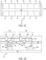
- FIG. 1C A schematic plan view of one embodiment of a stacked-substrate DRAM device 132 of the present disclosure appears in FIG. 1C . This figure is drawn primarily for convenience of explanation and comparison to FIG. 1A .
- FIG. 1D A cross-sectional view of a stacked-substrate device 132 appears in FIG. 1D .
- FIG. 1C A schematic plan view of one embodiment of a stacked-substrate DRAM device 132 of the present disclosure appears in FIG. 1C . This figure is drawn primarily for convenience of explanation and comparison to FIG. 1A .
- FIG. 1D A cross-sectional view of a stacked-substrate device 132 appears in FIG. 1D .
- FIG. 1D A schematic plan view of one embodiment of a stacked-substrate DRAM device 132 of the present disclosure appears in FIG. 1C . This figure is drawn primarily for convenience of explanation and comparison to FIG. 1A .
- FIG. 1D A cross-sectional view of
- the plan view illustrates memory arrays 104', areas associated with peripheral circuits 108', and vias 136, all of which are shown on a second substrate 106.
- the example device 132 includes an increased proportion of area for memory arrays 104' on the second substrate 106 surface and a decreased area for peripheral circuits 108' when compared to the device 100.
- the peripheral circuits 108' (or the portions thereof) that are present on the second substrate 106 are primarily those that connect the memory arrays 104' to the vias 136 (e.g., conductive lines between memory arrays 104' and vias 136).
- the semiconductor devices e.g., FinFET transistors
- the semiconductor devices e.g., FinFET transistors
- the first substrate of the stacked substrate device 132 includes at least some of the peripheral circuits 108' used to read from, write to, and address data to memory cells.
- FIG. 1D illustrates a cross sectional view of the stacked-substrate device 132.
- the cross-sectional view of the device 132 includes a first substrate 140, the second substrate 106 (visible in plan view FIG. 1C ), peripheral circuit semiconductor devices 142A, 142B, DRAM memory cells 144A, 144B, and via 136A.
- the cross-section is taken in a direction perpendicular to the word lines 154A, 154B of the memory array cells.
- the second substrate 106 is stacked over the first substrate 140 to form the stacked-substrate DRAM device 132.
- the second substrate 106 can be less than 200 nm or even less than 100 nm thick. This thickness of the second substrate 106 influences the depth of the via 136A. The thinner the substrate 106, generally the shorter the via 136A needed to place the bit line 148 in contact with a peripheral circuit. Vias 136A having a depth that is on the order of less than 200 nm or less than 100 nm are thus dimensioned similar to vias in "back end of line” (BEOL) interconnections, with similar electrical properties (e.g., low resistance).
- BEOL back end of line
- the DRAM memory cells 144A, 144B over the second substrate 106 includes capacitors 150A, 150B, bit line 148, and word lines 154A, 154B.
- the word lines include a gate dielectric layer 156A, 156B and a gate electrode 152A, 152B.
- the word lines can be biased on and off so as to selectively access stored charge (or lack thereof) in capacitors 150A, 150B when used in connection with the bit line 148.
- An isolation barrier 158 electrically isolates the word lines from one another.
- the isolation barrier 158 can be a recessed (e.g., 10-50 nm below a surface of the substrate 106) plug of dielectric material (e.g., SiO2) or can even be a "dummy" word line that is either always bias in an off state or is not electrically biased at all. In some examples, this isolation barrier 158 is formed using techniques applicable to the formation of shallow trench isolation or "STI.”
- STI shallow trench isolation
- FinFET semiconductor devices 142A, 142B are elements of peripheral circuits disposed on the first substrate 140 stacked below the second substrate 106. These schematically illustrated devices 142A, 142B can be used for any of the functions associated with writing to, reading from, addressing, or otherwise controlling the DRAM memory cells 144A, 144B. The fabrication of analogous devices is described below in more detail.
- FIG. 2 illustrates an example method 200 by which embodiments of the present disclosure can be fabricated.
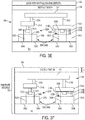
- FIGS. 3A-3G illustrate cross-sectional views of various stages of fabrication of the example method depicted in FIG. 2 . Concurrent reference to FIG. 2 and FIGS. 3A-3G will facilitate explanation.
- the method 200 includes providing 204 a first substrate 302 (as shown in FIG. 3A with various peripheral circuits, described in more detail below) and providing 205 a second substrate 304 (as shown in FIG. 3B ).
- peripheral circuits can be fabricated on the first substrate 302. These peripheral circuits can be used to write to, read from, and otherwise control memory cells and memory arrays of a DRAM device.
- the memory cells and the memory arrays formed by groups of individual memory cells) are fabricated on the second substrate 304.
- the substrate may be, for example, a bulk semiconductor wafer (e.g., bulk silicon, germanium, gallium arsenide or other III-V materials, etc.) or an on-insulator configuration (e.g., silicon on-insulator, germanium on-insulator, silicon germanium on-insulator, indium phosphide on-insulator, etc.).
- a bulk semiconductor wafer e.g., bulk silicon, germanium, gallium arsenide or other III-V materials, etc.
- an on-insulator configuration e.g., silicon on-insulator, germanium on-insulator, silicon germanium on-insulator, indium phosphide on-insulator, etc.
- the substrate may be: gallium nitride (GaN); c-axis aligned indium gallium zinc oxide (c-IGZO); transition metal dichalcogenides including but not limited to MoS2, MoSe2, CuS2, CuSe2, WS2, WSe2, among others; black phosphorus; or InGaAs.
- the substrate may be p-type, n-type, neutral-type, high or low resistivity, off-cut or not off-cut, etc.
- the substrate may have a vicinal surface that is prepared by off-cutting the substrate from an ingot, wherein substrate is off-cut at an angle between, for instance, 2° and 8° (e.g., 4° off-cut silicon). Note, however, the substrate need not have any such specific features, and that embodiments of the present disclosure can be implemented using any one of more of numerous different substrates.
- the thickness of the first substrate 302 can vary and in some embodiments, for example, is in the range of 100 nm to thousands of nanometers.
- the substrate may be subsequently thinned or removed (e.g., by way of backside polish or other suitable thinning/removal process), after formation of the interconnect structure and application of protective layer such as etch stop, passivation layer, interlayer dielectric (ILD), capping layer, etc.
- the thickness of the second substrate 304 as provided 205 can be of similar dimension to that of the first substrate 302. Techniques for thinning the second substrate 304 so as to maintain a height of a via through the second substrate to less than 100 nm or less than 200 nm are described below.
- semiconductor devices 306A, 306B can be formed 208 on the first substrate 302.
- peripheral circuits include, but are not limited to, sense amplifiers, multiplexers, row and column select circuitry, power select circuitry, among others.
- Conductive vias and conductive lines 314 can connect various semiconductor devices 306 together, thus forming peripheral circuits.
- the semiconductor devices 306A, 306B can be formed 208 using standard metal oxide semiconductor (MOS) processing, although any desired process technology can be used.
- MOS metal oxide semiconductor
- the semiconductor devices 306 of the peripheral circuits 306 can be formed 208 using fin-based semiconductor devices, including field effect transistors (also known as "FinFETs").
- a FinFET is a MOSFET transistor built around a thin strip of semiconductor material (generally referred to as a fin) that extends from and above an underlying substrate (in this case, the substrate 302).
- the conductive channel of the FinFET device resides on the outer portions of the fin adjacent to the gate dielectric.
- the fins 318 (318A, 318B in the example shown) of the semiconductor devices 306 include a salient feature composed of a semiconductor material and configured to extend from and above a substrate surface.
- a fin 318 of semiconductor material can be patterned (e.g., lithographically masked and then etched) from the first substrate 302 itself or from a layer of material formed on the substrate 302 that is compositionally different from the first substrate 302.
- Materials that are "compositionally different" or “compositionally distinct” as used herein refers to two materials that have different chemical compositions.
- compositional difference may be, for instance, by virtue of an element that is in one material but not the other (e.g., SiGe is compositionally different than silicon), or by way of one material having all the same elements as a second material but at least one of those elements is intentionally provided at a different concentration in one material relative to the other material (e.g., SiGe having 70 atomic percent germanium is compositionally different than from SiGe having 25 atomic percent germanium).
- the materials may also have distinct dopants (e.g., gallium and magnesium) or the same dopants but at differing concentrations.
- compositionally distinct materials may further refer to two materials that have different crystallographic orientations. For instance, (110) silicon is compositionally distinct or different from (100) silicon. Creating a stack of different orientations could be accomplished, for instance, with blanket wafer layer transfer.
- a gate structure 322 (322A, 322B on corresponding fins 318A, 318B) comprising at least one layer of gate dielectric 326 (326A, 326B on corresponding fins 318A, 318B) and at least one layer of gate electrode 330 (330A, 330B on corresponding fins 318A, 318B) can be fabricated on the one or more the fins 318.
- Examples of materials that can be used to form the gate dielectric layer 326 include, but are not limited to, dielectric materials used for interlayer dielectric (ILD) described below, as well as "high-k” materials, or both.
- High-k dielectric materials are those generally considered to have a dielectric constant greater than that of silicon dioxide and include, but are not limited to hafnium oxide, hafnium silicon oxide, lanthanum oxide, lanthanum aluminum oxide, zirconium oxide, zirconium silicon oxide, tantalum oxide, titanium oxide, barium strontium titanium oxide, strontium titanium oxide, yttrium oxide, aluminum oxide, lead scandium tantalum oxide, and lead zinc niobate.
- additional processing may be performed on the high-k dielectric layer, such as an annealing process, to improve the quality of high-k material.
- the portions of the fin 318 not covered by the gate structure 322 can be replaced with semiconductor material and/or doped to function as a source region 334 (334A, 334B on corresponding fins 318A, 318B) and a drain region 338 (338A, 338B on corresponding fins 318A, 318B).
- the portion of the fin 318 between the source region 334 and the drain region 338 and between the substrate 302 and the gate structure 322 is sometimes referred to as a semiconductor body and can be characterized as including a channel region 342 (342A, 342B on corresponding fins 318A, 318B) through which charge carriers can flow.
- a voltage can be applied to the gate structure to control the flow of charge carriers from the source region 334 to the drain region 338.
- a layer of dielectric material 346 (sometimes referred to as interlayer dielectric) can be formed 212 on the semiconductor devices 306.
- the dielectric layer (ILD) may include any number of conventional dielectric materials commonly used in integrated circuit applications, such as oxides (e.g., silicon dioxide, carbon doped oxide), silicon nitride, or organic polymers (e.g., perfluorocyclobutane or polytetrafluoroethylene), fluorosilicate glass, and organosilicates (e.g., silsesquioxane, siloxane, or organosilicate glass).
- the dielectric material may be low-k or high-k depending on the desired isolation, and may include pores or other voids to further reduce its dielectric constant.
- the dielectric layer thickness can vary and in some example embodiments is in the range of 50 nm to 5000 nm. In some embodiments, the dielectric layer may actually include multiple layers having the same or differing thicknesses. Likewise, in some embodiments, each ILD layer is implemented with the same dielectric material, but in other embodiments, at least some of the ILD layers are implemented with differing dielectric materials.
- the layer of dielectric material 346 can be any of a wide range of suitable deposition techniques, including but not necessarily limited to: physical vapor deposition (PVD); chemical vapor deposition (CVD); spin coating/spin-on deposition (SOD); and/or a combination of any of the aforementioned.
- PVD physical vapor deposition
- CVD chemical vapor deposition
- SOD spin coating/spin-on deposition
- Other suitable configurations, materials, deposition techniques, and/or thicknesses for base ILD layer 346 will depend on a given application and will be apparent in light of this disclosure. Numerous ILD configurations and dimensions will be apparent in light of this disclosure and the claimed invention is not intended to be limited to any particular configurations and dimensions.
- the ILD can be planarized and/or polished using any suitable technique including chemical-mechanical planarization/polishing (CMP) processes, for example.
- CMP chemical-mechanical planarization/polishing
- conductive interconnect structures e.g., contact structures or "vias” 310A, 310B, 315A, 315B
- conductive lines 314A, 314B, 317
- the electrical connection established by the conductive interconnect structures 310, 315, 314, 317 between semiconductor devices 306 thus forms the peripheral circuits (examples of which are described above) used to control the DRAM memory cells and arrays of memory cells.
- the conductive interconnections can be formed of the same materials, and in other cases, may include compositionally different materials, whether different from layer to layer and/or within the same layer.
- one or more of the vias 310, 315 and the conductive lines 314, 317 can include one or more layers of a conductive liner (e.g., silicon nitride, graphene, tantalum nitride) and one more layers of a conductive metal (e.g., copper, aluminum).
- a conductive liner e.g., silicon nitride, graphene, tantalum nitride
- a conductive metal e.g., copper, aluminum
- Formation 216 of these conductive interconnect structures can be performed by standard processes of photolithographic patterning and etching (e.g., removal of portions of the dielectric layer 346), followed by deposition of one or more layers in the patterned and etched regions of the dielectric layer 346.
- Example deposition techniques applicable to conductive material include but are not limited to sputtering, physical vapor deposition (PVD), chemical vapor deposition (CVD), metallo-organic CVD (MOCVD), among others.
- PVD physical vapor deposition
- CVD chemical vapor deposition
- MOCVD metallo-organic CVD
- metal lines and vias can be implemented as a dual damascene structure fabricated in the corresponding dielectric layer (ILD).
- the dual damascene trench can be formed in the dielectric layer, for example, using standard lithography including via and trench patterning and subsequent etch processes followed by polishing, cleans, etc., as typically done.
- the patterning and etch processes can be carried out, for instance, using wet and/or dry etch techniques.
- the trenches in the ILD in which vias and conductive lines are formed can have various dimensions depending on the application.
- an upper trench opening i.e., corresponding to a conductive line portion of a dual damascene via/conductive line structure
- a lower via opening is about 5 nm to 50 nm (e.g., 10 to 25 nm)
- the entire structure has an aspect ratio in the range of about 10:1 to 1.25:1 (e.g., 5:1).
- the dimensions and aspect ratio of the damascene trench will vary from one embodiment to the next, and the present disclosure is not intended to be limited to any particular range of dimensions, or any particular trench configuration.
- conductive interconnect cross-sections can include a profile having a first lateral width and a second lateral width that is smaller than the first lateral width, while in another example case the metal interconnect pathway cross-section demonstrates a profile having a substantially uniform lateral width from top to bottom.
- the conductive interconnections can be formed by first forming a blanket layer of conductive material followed by patterning and etching of the blanket layer into the conductive interconnect structures illustrated in FIG. 3A .
- the conductive interconnect structures formed in this way can be electrically isolated from one another by subsequent deposition of dielectric material, as described above.
- the layers of interconnection are demarcated from neighboring layers by an etch stop layer (e.g., a nitride layer) and may also include a barrier layer to prevent electromigration of material between adjacent conductive interconnect structures (e.g., nitride layers, among others).
- an etch stop layer e.g., a nitride layer
- barrier layer to prevent electromigration of material between adjacent conductive interconnect structures (e.g., nitride layers, among others).
- the method 200 also includes providing 205 a second semiconductor substrate 304, which in various embodiments can be any one of the substrate compositions or types previously described in the context of the first substrate 302.
- the final thickness of the second substrate as integrated into a stacked-substrate DRAM device is less than 200 nm or less than 100 nm so as to facilitate a similar depth (e.g., less than 200 nm or less than 100 nm) of a via connecting the DRAM memory cells to the peripheral circuits.
- the second substrate 304 can be first implanted 209 with, for example, accelerated hydrogen ions through one of the exposed surfaces.
- the accelerated hydrogen ions cause the formation of a sub-surface layer 350 with crystallographic defects that can be between from 5 nm to 500 nm below the surface through which the ions penetrate.
- the accelerated ions interact with atoms within the lattice of the second substrate 304 so as to displace some of the atoms from crystal lattice sites, thus forming vacancies within the crystalline lattice as one type of crystallographic defect.
- dislocations and dislocation loops can form as another type of crystallographic defect.
- the defective layer 350 formed is a location at which the substrate 304 will cleave upon heat treatment.
- implantation can be accomplished by accelerating hydrogen ions (formed by exposure of hydrogen gas to an electrically biased filament so as to form a hydrogen plasma) at voltages of anywhere between 20 keV to 100 keV. Implantation densities of on the order of 10 15 atoms/cm 3 to 10 22 atoms/cm 3 can be used to form the defective layer 350. In some examples, the implantation current is from 5 mA/cm 2 of substrate to 10 mA/cm 2 . In some examples, accelerated hydrogen ions within the previously indicated acceleration voltages and implantation densities are capable of producing on the order of from 10 20 vacancies/cm 3 to 10 23 vacancies/cm 3 .
- an accelerating voltage of 40 keV can produce an approximately normal distribution of vacancies from 1 nm to 700 nm below the exposed surface through which the hydrogen ions are implanted, with a median of the distribution at about 500 nm below the surface (+/- 50 nm).
- the defective layer 350 can have a thickness (measured perpendicular to the surface of the substrate 304 through which the accelerated ions pass) within any of the following ranges: from 5 nm to 50 nm; from 5 nm to 25 nm; from 5 nm to 10 nm; from 10 nm to 50 nm; from 25 nm to 50 nm.
- the accelerating voltage of the parting (hydrogen) ions can be selected so that a depth below the surface of the defective layer 350 is within a desired range according to standard techniques. For example, a greater accelerating voltage of the hydrogen ions will cause the hydrogen ions to impinge to a distance greater from the exposed surface than a lower accelerating voltage.
- the accelerating voltage is selected to cause the defective layer 350 to be within the range below the surface indicated above (i.e., from 5 nm to 500 nm below the exposed surface).
- accelerated particles including but not limited to helium ions, can be used to create the defective layer 350.
- the defective layer 350 can be considered to divide the second substrate 304 into a first portion 354 and a second portion 358 on opposing sides of the defective layer 350.
- a depth of the defective layer 350 essentially defines a thickness of the second portion 358.
- exposure 222 is to an oxygen plasma.
- exposure 222 can be to a UV enhanced ozone (O 3 ) plasma, an aqueous (H 2 O) ozone solution plasma, or any other plasma chemistry capable of terminating the exposed surfaces in hydroxyl (OH) groups.
- O 3 UV enhanced ozone
- H 2 O aqueous ozone solution plasma
- any other plasma chemistry capable of terminating the exposed surfaces in hydroxyl (OH) groups.
- FIG. 3D exposure 222 to the oxygen plasma creates layers 362A, 362B on the treated surfaces that include a plurality of hydroxyl groups.
- the method 200 continues by placing 226 the plasma treated surface of the second portion 358 of the second substrate 304 in contact with the plasma treated surface of the first substrate 302, thus bringing the layers 362A, 362B into contact with one another.
- This initial contact between the plasma treated surfaces can be performed at ambient temperature (e.g., between 20°C and 25°C) and ambient atmospheric pressure (e.g., 1 atmosphere +/- 5%).
- the two substrates 302, 304 are heated 226 at temperatures anywhere between 300°C and 400°C (within normal equipment variation and measurement tolerances of approximately +/-2°C) for between 10 minutes and 60 minutes in an inert atmosphere (e.g., N 2 , Ar).
- an inert atmosphere e.g., N 2 , Ar.
- a covalent bond is formed between the second portion 358 of the second substrate 304 and the ILD 346 of the first substrate 302, thus joining the two substrates together.
- the covalent bonds formed are silicon-oxygen-silicon bonds.
- the silicon-oxygen-silicon bonds that bridge the interface are strong enough so that no additional adhesive or connection is needed to bond the first substrate 302 to the second substrate 304.
- the heat 226 applied to the attached first substrate 302 and second substrate 304 also causes the separation 230 of the first portion 354 of the second substrate 304 from the layer with crystallographic defects 350. In some cases, this can be described as "exfoliation" of first portion 354 from the second substrate 304. As shown in FIG. 3E , in some cases some or all of the layer with crystallographic defects 350 remains on the second portion 358 after the heat induced separation 230 of the first portion 354. In some embodiments, any remaining layer 350 with crystallographic defects can be removed by standard polishing and planarization techniques, including but not limited to chemical mechanical polishing (CMP). In some examples, some of the material comprising the second portion 358 can be removed through continued chemical mechanical polishing so that a thickness (indicated in FIG.
- CMP chemical mechanical polishing
- 3F as dimension ⁇ ) can be within any of the following ranges: from 5 nm (nm) to 200 nm; from 5 nm to 100 nm; from 10 nm to 100 nm; from 10 nm to 50 nm; from 15 nm to 30 nm.
- the resulting structure, referred to herein as a substrate assembly 366, is shown in FIG. 3F .
- the fabrication of the second portion 358 can include the use of a silicon germanium (SiGe) layer.
- SiGe silicon germanium
- a SiGe layer (of from 10 nm thick to 30 nm thick) on the second substrate can be composed and formed to have a coherent and epitaxial interface (i.e., a lattice parameter mismatch of less than 2%) with the underlying substrate (e.g., a silicon substrate).
- a silicon layer of from 10 nm to 20 nm thick corresponding to the second portion 358 can then be formed (epitaxially and coherently) on the SiGe layer.
- the defective layer 350 can then be formed via ion implantation (as described above) on a side of the SiGe layer opposite that of the silicon layer corresponding to the second portion 358. After separation of the second portion 358 from the substrate, the crystallographically defective layer can be removed via CMP until the SiGe layer is exposed. Silicon can be selectively removed from SiGe using CMP processes that include ammonium hydroxide (NH 4 OH) or tetramethyl ammonium hydroxide (N(CH 3 ) 4 OH). In this way, the SiGe acts an "etch stop." In other words, the processes used to remove the silicon layer are composed so as to not remove the SiGe layer or remove it at a rate that is at least 5 times slower than silicon is removed.
- the etch composition can be changed so that the SiGe layer can be removed using a selective etch that removes SiGe but does not remove Si (e.g., KOH,).
- a SiGe layer as an etch stop as described above can, in some examples, enhance control of a thickness ⁇ of the second portion 358.
- DRAM cell components and memory arrays can be formed 234 on the exposed surface of the second portion 358 on a side opposite that of the first substrate 302 and associated peripheral circuits.
- the second portion 358 essentially becomes a semiconductor substrate on which semiconductor devices can be fabricated, as is explained below. Similar to the preceding cross-sections, the cross-section of FIG. 3G is taken perpendicular to word lines of the DRAM memory array.
- the portion of the embodiment of the stacked-substrate DRAM memory device 372 shown in FIG. 3G includes the substrate assembly 366, described above, as well as word lines 376, bit lines 380, capacitors 384, interconnections 388, and inter-substrate via 392.
- the word lines 376 control (colloquially, "gate") access between the bit lines 380 and their corresponding capacitors 384, the latter of which can store a bit of data.
- the word lines 376 are conductive lines often fabricated from silicon or some other conductive semiconductor material that can be biased to an on state and an off state, thus controlling access (e.g., reading from and writing to) the memory cell capacitors 384.
- the word lines 376 include a gate dielectric layer 377 and a gate electrode layer 378. Any of the materials described above in the context of FinFET gate dielectric and gate electrode layers are applicable to the corresponding word line 376.
- SiO 2 can be used as the gate dielectric layer 377 and Si as the gate electrode layer 378.
- the gate dielectric layer 377 and the gate electrode layer 378 can be fabricated from one or more layers.
- the layers can be compositionally similar or compositionally different.
- the word lines 376 have an arcuate transverse cross-sectional portion that is recessed into the second substrate 304.
- RCATs recessed channel access transistors
- These "recessed channel access transistors" (“RCATs”) can increase an effective channel length relative to devices that have a more rectangular cross-section. Longer effective channel length can reduce off state leakage current (“Ioff”), thus improving device performance.
- RCATs can be fabricated by using standard techniques to remove a portion of a substrate (or more generically a layer of semiconductor material that includes the substrate or is on the substrate, and that may or may not be doped in different examples) by, for example, lithographic patterning and etching.
- a gate dielectric layer 377 and gate electrode layer 378 (composed of any of the possible materials described above) can then be sequentially formed in the recess using standard techniques.
- a cross-sectional profile perpendicular to the gate of the word lines 376 such as that illustrated in FIG. 3G , may be curved or "arcuate.”
- a cross-sectional profile perpendicular to the gate of the word lines 376 can be rectangular. It will be appreciated that due to natural process variation, a cross-sectional profile of any shape may have curved portions and linear portions and otherwise not conform exactly to a geometric shape.
- RCATs are shown in FIG. 3G , it will be appreciated that any type of word line 376 configuration can be used in embodiments of the present disclosure. Regardless of the type of word line 376 used, it will be appreciated that the word lines 376 regulate access of the bit lines 380 (and access transistors, not shown) to the capacitors 384.
- Bit lines 380 can, in some examples, be fabricated using a dual damascene process within an ILD layer 390, as explained above.
- a trench having a first portion narrower than a second portion can be formed in dielectric layer 390 using standard lithographic patterning and etching techniques.
- Layer(s) of a liner e.g., tantalum, tantalum nitride, tungsten nitride
- conductive materials e.g., tungsten, copper, aluminum
- a single damascene process can be used to separately form the trenches corresponding to the vias 388 and bit lines 380, both of which are subsequently filled with liner(s) and conductive material(s), respectively.
- the capacitors 384 can be any type of capacitor compatible within a DRAM memory array, including the type shown in FIG. 3G , a capacitor over bit line (or "COB").
- COB capacitor over bit line
- the COB capacitor 384 illustrated in FIG. 3G is a metal-insulator-metal or "MIM" capacitor. It will be appreciated that the COB MIM capacitor 384 shown in FIG. 3G is selected only for convenience, and that other types of capacitors may be used in embodiments of the present disclosure.
- a dual damascene trench is formed in the dielectric layer 390.
- the narrower portion of the trench is filled with any required conductive liner(s) and then filled with a conductive material (e.g., copper, aluminum), thus forming corresponding ones of the via interconnection 388.
- the via interconnection 388 can then place the capacitor 384 in communication with the word line 376, the latter of which, as explained above, controls access between the bit line 380 and the capacitor 384.
- a conductive metal layer is conformally formed in the second portion of the trench. This conductive metal layer, formed on walls of the trench formed by the etched portion of the dielectric layer 390, forms the outermost metal layer of the MIM capacitor 384.
- a layer of dielectric material (e.g., a high k material) is then conformally formed on the conductive metal layer, followed by filling the remaining portion of the trench with a conductive material. This series of layers then forms the metal-insulator-metal structure of the MIM capacitor.
- An isolation barrier 379 is disposed between adjacent word lines 376 (e.g., STI or an unbiased "dummy" word line), as described above in the context of FIG. 1D .
- the memory arrays and peripheral circuits can be placed into contact (e.g., electrical communication) with one another.
- This can be accomplished by forming 238 a via 392 that extends from the bit line 380, through the dielectric layer 390, the second portion 358 of the second substrate, and the dielectric layer 346.
- the via 392 is connected to the conductive interconnection 317.
- a via 392 can extend to different levels of conductive interconnect or even to a contact on a drain region of a semiconductor device (e.g., contact structure 310B on drain region 338B).
- the via 392 can be formed 238 using standard techniques, such as lithographic patterning and etching. These have been described above in the context of interconnections 310, 314, 315, 317, among others, and need no further explanation.
- the placement of the via 392 can be selected using standard optical alignment techniques used to align various levels of interconnections.
- standard alignment techniques can be used to align the via 392 with corresponding structure (whether conductive interconnection of a peripheral circuit or semiconductor device) on the first substrate 302.
- these standard alignment techniques involve the use of alignment structures and/or patterns that can be used as reference points by which lithographic masks and other process tools can be aligned.
- some of the second portion 358 of the second substrate 304 can be removed (e.g., by lithographic patterning and etching) so that these alignment structures on the first substrate 302 (sometimes colloquially referred to as “fiducial structure” or “alignment marks”) can be detected.
- the formation of the via 392 can use techniques similar or the same as those used to form interconnections 315A, 315B, 310A, 310B. That is, standard single damascene or dual damascene techniques for the fabrication of vias between metal levels in a "back end of line” (BEOL) of an integrated circuit can be adapted to the via 392 by selecting processes that can pattern dielectric material 390, second substrate second portion 358 (whether silicon or some other composition), and then dielectric material 346.
- BEOL back end of line
- a depth of the via 392 can correspond to the thickness of the second portion 358 plus 5-10 nm above the surface (to contact to the bit line 380) and plus 5-10 nm below the second portion 358 (to contact peripheral circuit interconnections). In embodiments, a depth of the via 392 is less than 200 nm, less than 100 nm, less than 50 nm, or less than 20 nm.
- the depth of via 392 corresponding to (and in some cases 5 nm-20 nm greater than) the thickness ⁇ of the second portion 358 leads to a via 392 electrical resistance of from 1 Ohm to 40 Ohms or within any of the following sub-ranges: 1 Ohm to 5 Ohms; 1 Ohm to 10 Ohms; 10 Ohms to 30 Ohms; 15 Ohms to 35 Ohms.
- FIG. 4 is an example computing system implemented with one or more of the integrated circuit structures as disclosed herein, in accordance with some embodiments of the present disclosure.
- the computing system 400 houses a motherboard 402.
- the motherboard 402 may include a number of components, including, but not limited to, a processor 404 and at least one communication chip 406, each of which can be physically and electrically coupled to the motherboard 402, or otherwise integrated therein.
- the motherboard 402 may be, for example, any printed circuit board, whether a main board, a daughterboard mounted on a main board, or the only board of system 400, etc.
- computing system 400 may include one or more other components that may or may not be physically and electrically coupled to the motherboard 402. These other components may include, but are not limited to, volatile memory (e.g., DRAM), nonvolatile memory (e.g., ROM), a graphics processor, a digital signal processor, a crypto processor, a chipset, an antenna, a display, a touchscreen display, a touchscreen controller, a battery, an audio codec, a video codec, a power amplifier, a global positioning system (GPS) device, a compass, an accelerometer, a gyroscope, a speaker, a camera, and a mass storage device (such as hard disk drive, compact disk (CD), digital versatile disk (DVD), and so forth).
- volatile memory e.g., DRAM
- nonvolatile memory e.g., ROM
- graphics processor e.g., a digital signal processor
- crypto processor e.g., a graphics processor
- a digital signal processor e
- any of the components included in computing system 400 may include one or more integrated circuit structures or devices configured in accordance with an example embodiment (e.g., to include one or more stacked-substrate DRAM memory devices, as variously provided herein).
- multiple functions can be integrated into one or more chips (e.g., for instance, note that the communication chip 406 can be part of or otherwise integrated into the processor 404).
- the communication chip 406 enables wireless communications for the transfer of data to and from the computing system 400.
- wireless and its derivatives may be used to describe circuits, devices, systems, methods, techniques, communications channels, etc., that may communicate data through the use of modulated electromagnetic radiation through a non-solid medium. The term does not imply that the associated devices do not contain any wires, although in some embodiments they might not.
- the communication chip 406 may implement any of a number of wireless standards or protocols, including, but not limited to, Wi-Fi (IEEE 802.11 family), WiMAX (IEEE 802.16 family), IEEE 802.20, long term evolution (LTE), Ev-DO, HSPA+, HSDPA+, HSUPA+, EDGE, GSM, GPRS, CDMA, TDMA, DECT, Bluetooth, derivatives thereof, as well as any other wireless protocols that are designated as 3G, 4G, 5G, and beyond.
- the computing system 400 may include a plurality of communication chips 406.
- a first communication chip 406 may be dedicated to shorter range wireless communications such as Wi-Fi and Bluetooth and a second communication chip 406 may be dedicated to longer range wireless communications such as GPS, EDGE, GPRS, CDMA, WiMAX, LTE, Ev-DO, and others.
- communication chip 406 may include one or more transistor structures having a gate stack an access region polarization layer as variously described herein.
- the processor 404 of the computing system 400 includes an integrated circuit die packaged within the processor 404.
- the integrated circuit die of the processor includes onboard circuitry that is implemented with one or more integrated circuit structures or devices as variously described herein.
- the term "processor" may refer to any device or portion of a device that processes, for instance, electronic data from registers and/or memory to transform that electronic data into other electronic data that may be stored in registers and/or memory.
- the communication chip 406 also may include an integrated circuit die packaged within the communication chip 406.
- the integrated circuit die of the communication chip includes one or more integrated circuit structures or devices as variously described herein.
- multistandard wireless capability may be integrated directly into the processor 404 (e.g., where functionality of any chips 406 is integrated into processor 404, rather than having separate communication chips).
- processor 404 may be a chip set having such wireless capability.
- any number of processor 404 and/or communication chips 406 can be used.
- any one chip or chip set can have multiple functions integrated therein.
- the computing system 400 may be a laptop, a netbook, a notebook, a smartphone, a tablet, a personal digital assistant (PDA), an ultra-mobile PC, a mobile phone, a desktop computer, a server, a printer, a scanner, a monitor, a set-top box, an entertainment control unit, a digital camera, a portable music player, a digital video recorder, or any other electronic device that processes data or employs one or more integrated circuit structures or devices formed using the disclosed techniques, as variously described herein.
- PDA personal digital assistant
Landscapes
- Engineering & Computer Science (AREA)
- Manufacturing & Machinery (AREA)
- Semiconductor Memories (AREA)
Applications Claiming Priority (1)
| Application Number | Priority Date | Filing Date | Title |
|---|---|---|---|
| US16/140,890 US11569243B2 (en) | 2018-09-25 | 2018-09-25 | Stacked-substrate DRAM semiconductor devices |
Publications (2)
| Publication Number | Publication Date |
|---|---|
| EP3629374A2 true EP3629374A2 (de) | 2020-04-01 |
| EP3629374A3 EP3629374A3 (de) | 2020-07-22 |
Family
ID=67139616
Family Applications (1)
| Application Number | Title | Priority Date | Filing Date |
|---|---|---|---|
| EP19183099.1A Pending EP3629374A3 (de) | 2018-09-25 | 2019-06-28 | Stapelsubstrat-dram-halbleiterbauelemente |
Country Status (2)
| Country | Link |
|---|---|
| US (1) | US11569243B2 (de) |
| EP (1) | EP3629374A3 (de) |
Families Citing this family (7)
| Publication number | Priority date | Publication date | Assignee | Title |
|---|---|---|---|---|
| US9658281B2 (en) * | 2013-10-25 | 2017-05-23 | Taiwan Semiconductor Manufacturing Company Limited | Alignment testing for tiered semiconductor structure |
| KR102747694B1 (ko) * | 2020-08-25 | 2024-12-30 | 삼성전자주식회사 | 3차원 반도체 메모리 장치 |
| US11818877B2 (en) | 2020-11-02 | 2023-11-14 | Applied Materials, Inc. | Three-dimensional dynamic random access memory (DRAM) and methods of forming the same |
| US12616012B2 (en) * | 2021-08-19 | 2026-04-28 | Intel Corporation | Stacked random access memory devices with multilayer continuous vias |
| CN116234301B (zh) * | 2022-05-17 | 2024-03-15 | 北京超弦存储器研究院 | 一种半导体器件结构及其制造方法、dram和电子设备 |
| CN117915654A (zh) * | 2022-10-10 | 2024-04-19 | 长鑫存储技术有限公司 | 存储器及其制作方法、操作方法 |
| CN116863974B (zh) * | 2023-09-05 | 2023-11-21 | 北京超弦存储器研究院 | 半导体器件及电子设备 |
Citations (1)
| Publication number | Priority date | Publication date | Assignee | Title |
|---|---|---|---|---|
| US20150102395A1 (en) * | 2013-10-11 | 2015-04-16 | Jae-hwa Park | Semiconductor device including decoupling capacitor and method of forming the same |
Family Cites Families (7)
| Publication number | Priority date | Publication date | Assignee | Title |
|---|---|---|---|---|
| US6551857B2 (en) | 1997-04-04 | 2003-04-22 | Elm Technology Corporation | Three dimensional structure integrated circuits |
| TW587252B (en) | 2000-01-18 | 2004-05-11 | Hitachi Ltd | Semiconductor memory device and data processing device |
| US7800166B2 (en) | 2008-05-30 | 2010-09-21 | Intel Corporation | Recessed channel array transistor (RCAT) structures and method of formation |
| KR20090126077A (ko) | 2008-06-03 | 2009-12-08 | 삼성전자주식회사 | 메모리 반도체 장치 및 그 제조 방법 |
| DE112011105710T5 (de) | 2011-10-07 | 2014-06-26 | Intel Corporation | Bildung eines Dram-Kondensators unter einem Metall-Interconnect |
| WO2014071049A2 (en) * | 2012-10-31 | 2014-05-08 | Suvolta, Inc. | Dram-type device with low variation transistor peripheral circuits, and related methods |
| US11652606B2 (en) * | 2018-09-25 | 2023-05-16 | Intel Corporation | Advanced encryption standard semiconductor devices fabricated on a stacked-substrate |
-
2018
- 2018-09-25 US US16/140,890 patent/US11569243B2/en active Active
-
2019
- 2019-06-28 EP EP19183099.1A patent/EP3629374A3/de active Pending
Patent Citations (1)
| Publication number | Priority date | Publication date | Assignee | Title |
|---|---|---|---|---|
| US20150102395A1 (en) * | 2013-10-11 | 2015-04-16 | Jae-hwa Park | Semiconductor device including decoupling capacitor and method of forming the same |
Also Published As
| Publication number | Publication date |
|---|---|
| US20200098762A1 (en) | 2020-03-26 |
| EP3629374A3 (de) | 2020-07-22 |
| US11569243B2 (en) | 2023-01-31 |
Similar Documents
| Publication | Publication Date | Title |
|---|---|---|
| US11569243B2 (en) | Stacked-substrate DRAM semiconductor devices | |
| TWI609494B (zh) | 具有摻雜子鰭區域的非平面半導體裝置及其製造方法 | |
| CN107743653A (zh) | 用于半导体结构的金属特征的自底向上填充(buf) | |
| TWI874454B (zh) | 具有移除基板的環繞式閘極積體電路結構 | |
| TWI532185B (zh) | 有頂阻擋層的具有自對準鰭部的非平面半導體裝置 | |
| US20250029892A1 (en) | Integrated circuit structures having through-stack thermal sink for dual-sided devices | |
| US11652606B2 (en) | Advanced encryption standard semiconductor devices fabricated on a stacked-substrate | |
| US20230225098A1 (en) | Epitaxial features in semiconductor devices and method of forming the same | |
| US12087750B2 (en) | Stacked-substrate FPGA semiconductor devices | |
| US10177039B2 (en) | Shallow trench isolation structures and contact patterning | |
| US20240224536A1 (en) | Integrated circuit structures having layer select transistors for shared peripherals in memory | |
| US20250267886A1 (en) | Integrated circuit structures with void-free internal spacers | |
| JP2007311607A (ja) | 半導体装置の製造方法 | |
| US20240221821A1 (en) | Integrated circuit structures having two-transistor gain cell | |
| US20240215222A1 (en) | Integrated circuit structures having backside power delivery and signal routing for front side dram | |
| US20240332302A1 (en) | Integrated circuit structures with backside conductive source or drain contact having enhanced contact area | |
| US20240312991A1 (en) | Fabrication of gate-all-around integrated circuit structures having tuned upper nanowires | |
| US12610527B2 (en) | Integrated circuit structures having memory access transistor with backside contact | |
| US20240006531A1 (en) | Integrated circuit structures having vertical transistor | |
| US20240332166A1 (en) | Integrated circuit structures having air gaps | |
| US20240222360A1 (en) | Integrated circuit structures having stacked electrostatic discharge (esd) for backside power delivery | |
| US20240222520A1 (en) | Integrated circuit structures having vertical shared gate high-drive thin film transistors | |
| US20250006837A1 (en) | Integrated circuit structures having vertical-transport transistor with bottom source connection | |
| US20240222276A1 (en) | Integrated circuit structures having lookup table decoders for fpgas | |
| US20250210510A1 (en) | Integrated circuit structures with trench contact spacer structure |
Legal Events
| Date | Code | Title | Description |
|---|---|---|---|
| PUAI | Public reference made under article 153(3) epc to a published international application that has entered the european phase |
Free format text: ORIGINAL CODE: 0009012 |
|
| STAA | Information on the status of an ep patent application or granted ep patent |
Free format text: STATUS: THE APPLICATION HAS BEEN PUBLISHED |
|
| AK | Designated contracting states |
Kind code of ref document: A2 Designated state(s): AL AT BE BG CH CY CZ DE DK EE ES FI FR GB GR HR HU IE IS IT LI LT LU LV MC MK MT NL NO PL PT RO RS SE SI SK SM TR |
|
| AX | Request for extension of the european patent |
Extension state: BA ME |
|
| PUAL | Search report despatched |
Free format text: ORIGINAL CODE: 0009013 |
|
| AK | Designated contracting states |
Kind code of ref document: A3 Designated state(s): AL AT BE BG CH CY CZ DE DK EE ES FI FR GB GR HR HU IE IS IT LI LT LU LV MC MK MT NL NO PL PT RO RS SE SI SK SM TR |
|
| AX | Request for extension of the european patent |
Extension state: BA ME |
|
| RIC1 | Information provided on ipc code assigned before grant |
Ipc: H01L 27/06 20060101ALI20200618BHEP Ipc: H01L 27/108 20060101AFI20200618BHEP |
|
| STAA | Information on the status of an ep patent application or granted ep patent |
Free format text: STATUS: REQUEST FOR EXAMINATION WAS MADE |
|
| 17P | Request for examination filed |
Effective date: 20210122 |
|
| RBV | Designated contracting states (corrected) |
Designated state(s): AL AT BE BG CH CY CZ DE DK EE ES FI FR GB GR HR HU IE IS IT LI LT LU LV MC MK MT NL NO PL PT RO RS SE SI SK SM TR |
|
| STAA | Information on the status of an ep patent application or granted ep patent |
Free format text: STATUS: EXAMINATION IS IN PROGRESS |
|
| 17Q | First examination report despatched |
Effective date: 20230221 |