EP3629068B1 - Optischer add-/drop-multiplexer - Google Patents
Optischer add-/drop-multiplexer Download PDFInfo
- Publication number
- EP3629068B1 EP3629068B1 EP17913833.4A EP17913833A EP3629068B1 EP 3629068 B1 EP3629068 B1 EP 3629068B1 EP 17913833 A EP17913833 A EP 17913833A EP 3629068 B1 EP3629068 B1 EP 3629068B1
- Authority
- EP
- European Patent Office
- Prior art keywords
- waveguide
- layer waveguide
- width
- lower layer
- upper layer
- Prior art date
- Legal status (The legal status is an assumption and is not a legal conclusion. Google has not performed a legal analysis and makes no representation as to the accuracy of the status listed.)
- Active
Links
Images


Classifications
-
- G—PHYSICS
- G02—OPTICS
- G02B—OPTICAL ELEMENTS, SYSTEMS OR APPARATUS
- G02B6/00—Light guides; Structural details of arrangements comprising light guides and other optical elements, e.g. couplings
- G02B6/10—Light guides; Structural details of arrangements comprising light guides and other optical elements, e.g. couplings of the optical waveguide type
- G02B6/12—Light guides; Structural details of arrangements comprising light guides and other optical elements, e.g. couplings of the optical waveguide type of the integrated circuit kind
- G02B6/12007—Light guides; Structural details of arrangements comprising light guides and other optical elements, e.g. couplings of the optical waveguide type of the integrated circuit kind forming wavelength selective elements, e.g. multiplexer, demultiplexer
-
- G—PHYSICS
- G02—OPTICS
- G02B—OPTICAL ELEMENTS, SYSTEMS OR APPARATUS
- G02B6/00—Light guides; Structural details of arrangements comprising light guides and other optical elements, e.g. couplings
- G02B6/24—Coupling light guides
- G02B6/26—Optical coupling means
- G02B6/28—Optical coupling means having data bus means, i.e. plural waveguides interconnected and providing an inherently bidirectional system by mixing and splitting signals
- G02B6/293—Optical coupling means having data bus means, i.e. plural waveguides interconnected and providing an inherently bidirectional system by mixing and splitting signals with wavelength selective means
- G02B6/29379—Optical coupling means having data bus means, i.e. plural waveguides interconnected and providing an inherently bidirectional system by mixing and splitting signals with wavelength selective means characterised by the function or use of the complete device
- G02B6/2938—Optical coupling means having data bus means, i.e. plural waveguides interconnected and providing an inherently bidirectional system by mixing and splitting signals with wavelength selective means characterised by the function or use of the complete device for multiplexing or demultiplexing, i.e. combining or separating wavelengths, e.g. 1xN, NxM
- G02B6/29382—Optical coupling means having data bus means, i.e. plural waveguides interconnected and providing an inherently bidirectional system by mixing and splitting signals with wavelength selective means characterised by the function or use of the complete device for multiplexing or demultiplexing, i.e. combining or separating wavelengths, e.g. 1xN, NxM including at least adding or dropping a signal, i.e. passing the majority of signals
- G02B6/29383—Adding and dropping
-
- G—PHYSICS
- G02—OPTICS
- G02B—OPTICAL ELEMENTS, SYSTEMS OR APPARATUS
- G02B6/00—Light guides; Structural details of arrangements comprising light guides and other optical elements, e.g. couplings
- G02B6/02—Optical fibres with cladding with or without a coating
- G02B6/036—Optical fibres with cladding with or without a coating core or cladding comprising multiple layers
- G02B6/03616—Optical fibres characterised both by the number of different refractive index layers around the central core segment, i.e. around the innermost high index core layer, and their relative refractive index difference
- G02B6/03638—Optical fibres characterised both by the number of different refractive index layers around the central core segment, i.e. around the innermost high index core layer, and their relative refractive index difference having 3 layers only
-
- G—PHYSICS
- G02—OPTICS
- G02B—OPTICAL ELEMENTS, SYSTEMS OR APPARATUS
- G02B6/00—Light guides; Structural details of arrangements comprising light guides and other optical elements, e.g. couplings
- G02B6/10—Light guides; Structural details of arrangements comprising light guides and other optical elements, e.g. couplings of the optical waveguide type
- G02B6/12—Light guides; Structural details of arrangements comprising light guides and other optical elements, e.g. couplings of the optical waveguide type of the integrated circuit kind
- G02B6/122—Basic optical elements, e.g. light-guiding paths
- G02B6/1228—Tapered waveguides, e.g. integrated spot-size transformers
-
- G—PHYSICS
- G02—OPTICS
- G02B—OPTICAL ELEMENTS, SYSTEMS OR APPARATUS
- G02B6/00—Light guides; Structural details of arrangements comprising light guides and other optical elements, e.g. couplings
- G02B6/10—Light guides; Structural details of arrangements comprising light guides and other optical elements, e.g. couplings of the optical waveguide type
- G02B6/12—Light guides; Structural details of arrangements comprising light guides and other optical elements, e.g. couplings of the optical waveguide type of the integrated circuit kind
- G02B6/122—Basic optical elements, e.g. light-guiding paths
- G02B6/124—Geodesic lenses or integrated gratings
-
- G—PHYSICS
- G02—OPTICS
- G02B—OPTICAL ELEMENTS, SYSTEMS OR APPARATUS
- G02B6/00—Light guides; Structural details of arrangements comprising light guides and other optical elements, e.g. couplings
- G02B6/24—Coupling light guides
- G02B6/26—Optical coupling means
- G02B6/28—Optical coupling means having data bus means, i.e. plural waveguides interconnected and providing an inherently bidirectional system by mixing and splitting signals
- G02B6/293—Optical coupling means having data bus means, i.e. plural waveguides interconnected and providing an inherently bidirectional system by mixing and splitting signals with wavelength selective means
- G02B6/29379—Optical coupling means having data bus means, i.e. plural waveguides interconnected and providing an inherently bidirectional system by mixing and splitting signals with wavelength selective means characterised by the function or use of the complete device
- G02B6/29395—Optical coupling means having data bus means, i.e. plural waveguides interconnected and providing an inherently bidirectional system by mixing and splitting signals with wavelength selective means characterised by the function or use of the complete device configurable, e.g. tunable or reconfigurable
-
- H—ELECTRICITY
- H04—ELECTRIC COMMUNICATION TECHNIQUE
- H04J—MULTIPLEX COMMUNICATION
- H04J14/00—Optical multiplex systems
- H04J14/02—Wavelength-division multiplex systems
- H04J14/0201—Add-and-drop multiplexing
- H04J14/0202—Arrangements therefor
- H04J14/021—Reconfigurable arrangements, e.g. reconfigurable optical add/drop multiplexers [ROADM] or tunable optical add/drop multiplexers [TOADM]
Definitions
- This application relates to the field of optoelectronic technologies, and in particular, to an optical add/drop multiplexer.
- optical add/drop multiplexer is an important filtering device in an optical network, and emergence of the optical add/drop multiplexer enables the optical network to evolve from a point-to-point network to a complex ring network.
- Implementation of diverse optoelectronic functional devices benefits from development of a silicon optical technology.
- the optical add/drop multiplexer (Optical Add-Drop Multiplexer, OADM) based on the silicon optical technology mainly includes a microring and a Bragg grating.
- a conventional OADM having a single Bragg grating waveguide as long as incident light meets a Bragg grating condition, the incident light is reflected in the Bragg grating waveguide, and leaves from an input port, thereby implementing a selective drop of a specific wavelength.
- an external circulator or a Y branch structure usually needs to be used at the input port.
- the conventional OADM having a Bragg grating waveguide mainly uses a reflection condition of the Bragg grating in a lowest-order mode (for example, a 0-order mode).
- Bandwidth of a reflectance spectrum of the Bragg grating is determined based on a coupling factor of a forward mode and a backward mode in the Bragg grating waveguide.
- Three factors namely a degree of similarity between the two modes, a grating size, and restriction of a waveguide on light, affect the coupling factor. When each of the three factors is relatively large, the coupling factor increases.
- mainly Bragg reflection between a forward 0-order mode and a backward 0-order mode is used in the Bragg grating waveguide, and the two modes have a relatively high similarity. Because light is restricted in the single Bragg grating waveguide, the waveguide also has very strong restriction on light.
- CMOS Complementary Metal Oxide Semiconductor, complementary metal-oxide-semiconductor
- DWDM Dense Wavelength Division Multiplexing, dense wavelength division multiplexing
- JP 2016 024298 A discloses an optical waveguide device which equalizes the polarized-wave of an optical input signal with either one of a TE polarized-wave and a TM polarized wave, and outputs it.
- WO 2016/179869 A1 discloses a tapered waveguide and silicon-based chip.
- Embodiments of this application provide an optical add/drop multiplexer, so that a Bragg grating of a relatively large size is used, thereby reducing a processing difficulty.
- an optical add/drop multiplexer includes a drop signal separator and a drop signal reflector.
- the drop signal separator is connected to a main input end and a drop end; the drop signal separator is connected to the drop signal reflector, and the drop signal reflector is connected to a main output end; and an input end of the drop signal separator is configured to receive optical signals that are in a first mode, and transfer the optical signals that are in the first mode to the drop signal reflector in a single-layer waveguide transmission mode.
- the drop signal reflector includes a first transmission mode converter, a Bragg grating waveguide, and a second transmission mode converter.
- the first transmission mode converter includes a first upper layer waveguide and a first lower layer waveguide, the first upper layer waveguide is located above the first lower layer waveguide, the first upper layer waveguide and the first lower layer waveguide are connected to the drop signal separator, and the first transmission mode converter is configured to convert, into a double-layer waveguide transmission mode, the single-layer waveguide transmission mode in which the drop signal separator sends the optical signals that are in the first mode.
- the Bragg grating waveguide includes a second upper layer waveguide and a second lower layer waveguide, the second upper layer waveguide is located above the second lower layer waveguide, and the second lower layer waveguide is connected to the first lower layer waveguide; and a width of the second upper layer waveguide regularly changes with a first width alternating with a second width, to form a Bragg grating, where the first width is greater than the second width, the second upper layer waveguide is connected to the first upper layer waveguide, and the Bragg grating waveguide is configured to: receive the optical signals that are in the first mode and that are sent by the first transmission mode converter; and reflect, to the first transmission mode converter as an optical signal that is in a second mode, an optical signal that has a predetermined wavelength and that is of the optical signals that are in the first mode; and is further configured to send, to the second transmission mode converter, another optical signal of the optical signals that are in the first mode except the optical signal having the predetermined wavelength.
- the second transmission mode converter includes a third upper layer waveguide and a third lower layer waveguide, the third upper layer waveguide is located above the third lower layer waveguide, two ends of the third upper layer waveguide are respectively connected to the second upper layer waveguide and the main output end, and the third lower layer waveguide is connected to the second lower layer waveguide; and the second transmission mode converter is configured to convert a transmission mode of the another optical signal into the single-layer waveguide transmission mode, and output the another optical signal by using the main output end.
- the first transmission mode converter is further configured to convert the optical signal that is in the second mode into the single-layer waveguide transmission mode and output the optical signal to the drop signal separator, and the drop signal separator is further configured to output the optical signal that is in the second mode by using the drop end.
- the drop signal reflector includes a double-layer waveguide structure, and the double-layer waveguide structure reduces restriction on light. Therefore, the Bragg grating can reduce coupling between incident signal light that is in the first mode and reflected signal light that is in the second mode. In this way, to achieve reflectance spectrum bandwidth same as that required in the prior art, a larger grating size can be used, lowering a process requirement.
- the drop signal separator includes a first waveguide and a second waveguide, an input end of the first waveguide and an output end of the second waveguide are on a same plane, and an output end of the first waveguide and an input end of the second waveguide are on a same plane; and a width of the first waveguide at the input end is equal to a width of the second waveguide at the output end, a width of the first waveguide linearly increases from the input end to the output end, a width of the second waveguide linearly decreases from the output end to the input end, the output end of the first waveguide is connected to the first upper layer waveguide and the first lower layer waveguide, the input end of the first waveguide is used as a main input end of the drop signal separator, and the output end of the second waveguide is used as a drop end of the drop signal separator.
- the width of the first waveguide and the width of the second waveguide inversely change. Consequently, an index of refraction of the optical signal that is in the first mode by the first waveguide and an index of effective refraction of the optical signal that is in the second mode by the second waveguide cross each other.
- the index of refraction of the optical signal that is in the first mode by the first waveguide is equal to the index of effective refraction of the optical signal that is in the second mode by the second waveguide. Therefore, the optical signal that is in the second mode can be output from the second waveguide, thereby reducing a loss of separating drop signals.
- a width of an input end of the first upper layer waveguide is equal to a width of the output end of the first waveguide, and a width of the first upper layer waveguide is equal to the second width; and a width of an input end of the first lower layer waveguide is equal to the width of the output end of the first waveguide, a width of an output end of the first lower layer waveguide is greater than the first width, and a width of the first lower layer waveguide linearly increases from the input end to the output end.
- a thickness of the first upper layer waveguide is greater than a thickness of the first lower layer waveguide.
- a width of an input end of the second upper layer waveguide is equal to the second width, and a width of an output end of the second upper layer waveguide is equal to the second width; and a width of an input end of the second lower layer waveguide is equal to a width of an output end of the first lower layer waveguide, a width of an output end of the second lower layer waveguide is equal to the width of the output end of the first lower layer waveguide, and a width of the second lower layer waveguide is constant.
- a thickness of the second upper layer waveguide is greater than a thickness of the second lower layer waveguide.
- a width of an input end of the third upper layer waveguide is equal to the second width, and a width of the third upper layer waveguide linearly decreases from the input end to an output end; and a width of an input end of the third lower layer waveguide is equal to a width of an output end of the second lower layer waveguide, a width of an output end of the third lower layer waveguide is equal to a width of the output end of the third upper layer waveguide, and a width of the third lower layer waveguide linearly decreases from the input end to the output end.
- a thickness of the third upper layer waveguide is greater than a thickness of the third lower layer waveguide.
- the first upper layer waveguide, the second upper layer waveguide, and the third upper layer waveguide are identical in thickness; and the first lower layer waveguide, the second lower layer waveguide, and the third lower layer waveguide are identical in thickness.
- the first mode is a 0-order mode
- the second mode is a 1-order mode
- the first mode is a 1-order mode
- the second mode is a 0-order mode
- An optical add/drop multiplexer provided in the embodiments of this application is applied to an optical network that uses an optical fiber as a main transmission medium, such as a wide area network, a metropolitan area network, a newly established local area network with a large coverage.
- the optical add/drop multiplexer is mainly applied to a node that is in the optical network and that needs to upload and download a signal with a specific wavelength.
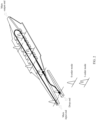
- an embodiment of this application provides an optical add/drop multiplexer, including: a drop signal separator 11 and a drop signal reflector 12.
- the drop signal reflector 12 includes a first transmission mode converter 121, a Bragg grating waveguide 122, and a second transmission mode converter 123.
- a structure of the optical add/drop multiplexer is divided by using dashed lines AA', BB', CC', DD', and EE'.
- the drop signal separator 11 is between AA' and BB'.
- the drop signal reflector 12 is between AA' and EE'.
- the first transmission mode converter 121 is between BB' and CC'.
- the Bragg grating waveguide 122 is between BB' and DD'.
- the second transmission mode converter 123 is between BB' and EE'.
- the drop signal separator 11 is connected to a main input end and a drop end; the drop signal separator 11 is connected to the drop signal reflector 12, and the drop signal reflector 12 is connected to a main output end main output.
- An input end of the drop signal separator 11 is configured to receive optical signals that are in a first mode, and transfer the optical signals that are in the first mode to the drop signal reflector 12 in a single-layer waveguide transmission mode.
- the drop signal reflector 12 is configured to reflect an optical signal that has a predetermined wavelength and that is of the optical signals that are in the first mode to the drop signal separator 11 in a second mode, and output the optical signal from the drop end drop.
- the drop signal reflector 12 is further configured to output, by using the main output end main output, another optical signal of the optical signals that are in the first mode except the optical signal having the predetermined wavelength.
- the drop signal separator 11 includes a first waveguide 111 and a second waveguide 112. An input end of the first waveguide 111 and an output end of the second waveguide 112 are on a same plane, and an output end of the first waveguide 111 and an input end of the second waveguide 112 are on a same plane.
- a width of the first waveguide 111 at the input end is equal to a width of the second waveguide 112 at the output end, a width of the first waveguide 111 linearly increases from the input end to the output end, a width of the second waveguide 112 linearly decreases from the output end to the input end, the input end of the first waveguide 111 is used as a main input end mian input of the drop signal separator 11, and the output end of the second waveguide 112 is used as a drop end drop of the drop signal separator 11.
- the drop signal separator 11 includes two waveguides that are placed in a signal propagation direction and whose widths inversely change.
- the width of the first waveguide 111 increases, and the width of the second waveguide 112 decreases.
- the two waveguides have a same width on an AA' plane, and both meet a single-mode waveguide condition in the silicon optical field.
- the two waveguides have a same length, and a spacing is relatively small, so that optical coupling between predetermined modes can be met.
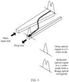
- the optical signals in the first mode from the outside first enters, from AA', a left-side port (that is, the main input end main input) of the first waveguide 111, and are propagated along the first waveguide 111.
- a modal refractive index for the input optical signal that is in the first mode increases as a waveguide width increases in a propagation process
- the modal refractive index for the optical signal transmitted in the first waveguide 111 continuously increases.
- a modal refractive index of the adjacent second waveguide continuously decreases. Therefore, modal refractive indexes of the two waveguides are not equal at any propagation location of the two waveguides. In other words, a phase matching condition of mode coupling is not met. Therefore, the input optical signal that is in the first mode directly passes the first waveguide 111, and is not coupled into the adjacent second waveguide 112. Eventually, the optical signal enters the drop signal reflector 12.
- the first waveguide 111 is a strip-shaped waveguide, the optical signal in the first waveguide is transmitted in the single-layer waveguide transmission mode.
- the first transmission mode converter 121 includes a first upper layer waveguide 1211 and a first lower layer waveguide 1212.
- the first upper layer waveguide 1211 is located above the first lower layer waveguide 1212, and the first upper layer waveguide 1211 and the first lower layer waveguide 1212 are connected to the drop signal separator 11.
- the first transmission mode converter 121 is configured to convert, into a double-layer waveguide transmission mode, the single-layer waveguide transmission mode in which the drop signal separator 11 sends the optical signals that are in the first mode.
- the first upper layer waveguide 1211 and the first lower layer waveguide 1212 are connected to the output end of the first waveguide 111.
- the optical signal first passes the first transmission mode converter 121.
- the first transmission mode converter 121 is configured to convert the single-layer waveguide (the first waveguide 111) transmission mode of the optical signal into the double-layer (the first upper layer waveguide 1211 and the first lower layer waveguide 1212) transmission mode.
- a width of an input end of the first upper layer waveguide 1211 is equal to a width of the output end of the first waveguide 111.
- a waveguide width of the first upper layer waveguide 1211 remains constant.
- a width of an input end of the first lower layer waveguide 1212 is equal to the width of the output end of the first waveguide 111, and a width of the first lower layer waveguide 1212 linearly increases from the input end to an output end.
- a sum of a thickness of the first upper layer waveguide 1211 and a thickness of the first lower layer waveguide 1212 is equal to a thickness of the first waveguide 111.
- the first transmission mode converter 121 has a sufficient length. This ensures a very small loss in a mode conversion process, in which 0-order mode output is still kept for 0-order mode input, or 1-order mode output is still kept for 1-order mode input. Then the optical signal continues to enter the Bragg grating waveguide 122.
- the Bragg grating waveguide 122 includes a second upper layer waveguide 1221 and a second lower layer waveguide 1222.
- the second upper layer waveguide 1221 is located above the second lower layer waveguide 1222, and the second lower layer waveguide 1222 is connected to the first lower layer waveguide 1212.
- a width of the second upper layer waveguide 1221 regularly changes with a first width alternating with a second width, to form a Bragg grating.
- the first width is greater than the second width, and the second upper layer waveguide 1221 is connected to the first upper layer waveguide 1211.
- the Bragg grating waveguide 122 is configured to: receive the optical signals that are in the first mode sent by the first transmission mode converter 121; and reflect, to the first transmission mode converter 121 as an optical signal that is in the second mode, an optical signal that has a predetermined wavelength and that is of the optical signals that are in the first mode; and is further configured to send, to the second transmission mode converter 123, another optical signal of the optical signals that are in the first mode except the optical signal having the predetermined wavelength.
- a Bragg reflection condition of the Bragg grating meets that an incident optical signal in the first mode is reflected in the second mode.
- the first mode is a 0-order mode (TE 0 ), and the second mode is a 1-order mode (TE 1 ); or the first mode is a 1-order mode, and the second mode is a 0-order mode.
- a width of an input end of the second upper layer waveguide 1221 is equal to the second width
- a width of an output end of the second upper layer waveguide 1222 is equal to the second width.
- a width of a lower layer waveguide, namely the second lower layer waveguide 1222, of the Bragg grating waveguide 122 is consistent with an end width of a lower layer waveguide, namely the first lower layer waveguide 1212, of the first transmission mode converter 121; a width of an upper layer waveguide, namely the second upper layer waveguide 1221, regularly changes; the smaller second width is the same as an end width of an upper layer waveguide, namely the first upper layer waveguide 1211, of the first transmission mode converter 121; the larger first width is less than the width of the second lower layer waveguide 1222; a width of an output end of the second lower layer waveguide 1222 is equal to a width of an output end of the first lower layer waveguide 1212; and the width of the second lower layer waveguide 1222 is constant, thereby forming the Bragg grating.
- a larger first width size of the second upper layer waveguide 1221 and period selection can enable a forward 0-order mode and a backward 1-order mode to meet the Bragg reflection condition.
- the optical signal that is input in the 0-order mode is reflected in the 1-order mode instead of passing the drop signal reflector 12.
- Bandwidth of a Bragg reflectance spectrum is determined based on a coupling factor of a forward mode and a backward mode in the Bragg grating waveguide 122. Three factors, namely a degree of similarity between the two modes, a grating size, and restriction of a waveguide on light, affect the coupling factor.
- the coupling factor increases.
- mainly Bragg reflection between a forward 0-order mode and a backward 0-order mode is used in a Bragg grating waveguide, and the two modes have a relatively high similarity.
- the two modes have a very low similarity.
- the Bragg grating waveguide uses a double-layer waveguide structure, and the second lower layer waveguide at a lower layer in the double-layer waveguide structure is relatively wide. In other words, there is a relatively large waveguide portion having a high refractive index in the Bragg grating waveguide.
- processing of the optical signal by the Bragg grating waveguide 122 includes two cases. In a first case, a wavelength of the optical signal meets a Bragg reflection condition, and the optical signal is reflected back to the first transmission mode converter 121. In a second case, a wavelength of the optical signal does not meet a Bragg reflection condition, and the optical signal is not reflected, but directly passes the Bragg grating waveguide 122 and enters the second transmission mode converter 123.
- the second transmission mode converter 123 includes a third upper layer waveguide 1231 and a third lower layer waveguide 1232.
- the third upper layer waveguide 1231 is located above the third lower layer waveguide 1232, two ends of the third upper layer waveguide 1231 are respectively connected to the second upper layer waveguide 1221 and the main output end main output, and the third lower layer waveguide 1232 is connected to the second lower layer waveguide 1222.
- the second transmission mode converter 123 is configured to convert a transmission mode of the another optical signal into the single-layer waveguide transmission mode, and output the another optical signal by using the main output end main output.
- a width of an input end of the third upper layer waveguide 1231 is equal to the second width, and a width of the third upper layer waveguide 1231 linearly decreases from the input end to an output end.
- a width of an input end of the third lower layer waveguide 1232 is equal to the width of the output end of the second lower layer waveguide 1222, a width of an output end of the third lower layer waveguide 1232 is equal to a width of the output end of the third upper layer waveguide 1231, and a width of the third lower layer waveguide 1232 linearly decreases from the input end to the output end.
- the first transmission mode converter 121 is further configured to convert the optical signal that is in the second mode into the single-layer waveguide transmission mode and output the optical signal to the drop signal separator 11, and the drop signal separator 11 is further configured to output the optical signal that is in the second mode by using the drop end drop.
- the first transmission mode converter 121 in the first case in which the Bragg grating waveguide 122 processes the optical signal, in other words, when a wavelength of signal light meets the Bragg reflection condition, the optical signal is reflected back to the first upper layer waveguide 1221 of the first transmission mode converter 121 in the 1-order mode.
- an effective refractive index in the 1-order mode is less than an effective refractive index in the 0-order mode. Therefore, at a location (for example, a location a shown in FIG. 4 ), an effective refractive index of the first waveguide 111 in the 1-order mode is the same as an effective refractive index of the second waveguide 112 in the 0-order mode. In short, a phase matching relationship is met.
- the optical signal in the 1-order mode in the first waveguide 111 is slowly coupled into the 0-order mode for the second waveguide 112, and is eventually output from a left-side port (the drop end drop) of the second waveguide 112, to complete a drop function.
- the Bragg grating waveguide 122 processes the optical signal
- the optical signal is not reflected, but directly passes the Bragg grating waveguide 122 in the 0-order mode and enters the second transmission mode converter 123.
- the width of an upper layer waveguide, namely the third upper layer waveguide 1231, of the second transmission mode converter 123 decreases, and a maximum width value is the same as the width of the lower layer waveguide, namely the second lower layer waveguide 1222, of the Bragg grating waveguide 122.
- the width of the third upper layer waveguide 1231 decreases, and a maximum width value is the same as a smaller value (the second width) of the width of the upper layer waveguide, namely the second upper layer waveguide 1221, of the Bragg grating waveguide 122.
- the width of the output end of the third lower layer waveguide 1232 is equal to the width of the output end of the third upper layer waveguide 1231, and both waveguides meet a single-mode condition in a silicon photonics field.
- a role of the second transmission mode converter 123 is to convert the double-layer waveguide (the third upper layer waveguide 1231 and the third lower layer waveguide 1232) transmission mode of the optical signal into the single-layer waveguide transmission mode, so that the optical signal is transmitted on an optical fiber connected to the main output end main output.
- the optical signal passing through the second transmission mode converter 123 is output from the main output end main output at EE'.
- a thickness of the first upper layer waveguide is greater than a thickness of the first lower layer waveguide
- a thickness of the second upper layer waveguide is greater than a thickness of the second lower layer waveguide
- a thickness of the third upper layer waveguide is greater than a thickness of the third lower layer waveguide.
Landscapes
- Physics & Mathematics (AREA)
- General Physics & Mathematics (AREA)
- Optics & Photonics (AREA)
- Engineering & Computer Science (AREA)
- Microelectronics & Electronic Packaging (AREA)
- Power Engineering (AREA)
- Computer Networks & Wireless Communication (AREA)
- Signal Processing (AREA)
- Optical Integrated Circuits (AREA)
Claims (10)
- Optischer Add-/Drop-Multiplexer, umfassend einen Drop-Signalseparator (11) und einen Drop-Signalreflektor (12), wobei der Drop-Signalseparator (11) mit einem Haupteingangsende und einem Drop-Ende verbunden ist; der Drop-Signalseparator mit dem Drop-Signalreflektor verbunden ist und der Drop-Signalreflektor mit einem Hauptausgangsende verbunden ist; und ein Eingangsende des Drop-Signalseparators dazu konfiguriert ist, optische Signale, die sich in einem ersten Modus befinden, zu empfangen und die optischen Signale, die sich in dem ersten Modus befinden, in einem einschichtigen Wellenleiterübertragungsmodus an den Drop-Signalreflektor zu übertragen;der Drop-Signalreflektor (12) einen ersten Übertragungsmoduskonverter (121), einen Bragg-Gitter-Wellenleiter (122) und einen zweiten Übertragungsmoduskonverter (123) umfasst;der erste Übertragungsmoduskonverter (121) einen ersten Wellenleiter der oberen Schicht (1211) und einen ersten Wellenleiter der unteren Schicht (1212) umfasst, wobei der erste Wellenleiter der oberen Schicht (1211) über dem ersten Wellenleiter der unteren Schicht (1212) angeordnet ist, wobei der erste Wellenleiter der oberen Schicht (1211) und der erste Wellenleiter der unteren Schicht (1212) mit dem Drop-Signalseparator (11) verbunden sind und der erste Übertragungsmoduskonverter (121) dazu konfiguriert ist, den einschichtigen Wellenleiterübertragungsmodus, in dem der Drop-Signalseparator (11) die optischen Signale sendet, die sich im ersten Modus befinden, in einen zweischichtigen Wellenleiterübertragungsmodus umzuwandeln;der Bragg-Gitter-Wellenleiter (122) einen Wellenleiter der zweiten oberen Schicht (1221) und einen Wellenleiter der zweiten unteren Schicht (1222) umfasst, wobei sich der Wellenleiter der zweiten oberen Schicht (1221) über dem Wellenleiter der zweiten unteren Schicht (1222) befindet und der Wellenleiter der zweiten unteren Schicht (1222) mit dem Wellenleiter der ersten unteren Schicht (1212) verbunden ist; und eine Breite des Wellenleiters der zweiten oberen Schicht (1221) sich regelmäßig ändert, wobei sich eine erste Breite mit einer zweiten Breite abwechselt, um ein Bragg-Gitter zu bilden, wobei die erste Breite größer als die zweite Breite ist, der Wellenleiter der zweiten oberen Schicht (1221) mit dem Wellenleiter der ersten oberen Schicht (1211) verbunden ist und der Bragg-Gitter-Wellenleiter zu Folgendem konfiguriert ist: Empfangen der optischen Signale, die sich im ersten Modus befinden und die vom ersten Übertragungsmoduskonverter (121) gesendet werden; und Reflektieren eines optischen Signals, das eine vorgegebene Wellenlänge aufweist und zu den optischen Signalen gehört, die sich im ersten Modus befinden, als optisches Signal, das sich im zweiten Modus befindet, an den ersten Übertragungsmoduskonverter (121); und ist ferner dazu konfiguriert, ein anderes optisches Signal der optischen Signale, die sich im ersten Modus befinden, an den zweiten Übertragungsmoduskonverter (123) zu senden, mit Ausnahme des optischen Signals mit der vorgegebenen Wellenlänge;der zweite Übertragungsmoduskonverter (123) einen dritten Wellenleiter der oberen Schicht (1231) und einen dritten Wellenleiter der unteren Schicht (1232) umfasst, wobei sich der dritte Wellenleiter der oberen Schicht (1231) über dem dritten Wellenleiter der unteren Schicht (1232) befindet, zwei Enden des dritten Wellenleiters der oberen Schicht (1231) jeweils mit dem zweiten Wellenleiter der oberen Schicht (1221) und dem Hauptausgangsende verbunden sind und der dritte Wellenleiter der unteren Schicht (1232) mit dem zweiten Wellenleiter der unteren Schicht (1222) verbunden ist; und der zweite Übertragungsmoduskonverter (123) dazu konfiguriert ist, einen Übertragungsmodus des anderen optischen Signals in den Einschicht-Wellenleiter-Übertragungsmodus umzuwandeln und das andere optische Signal unter Verwendung des Hauptausgangsendes auszugeben; undder erste Übertragungsmoduskonverter (121) ferner dazu konfiguriert ist, das im zweiten Modus befindliche optische Signal in den Einschicht-Wellenleiter-Übertragungsmodus umzuwandeln und das optische Signal an den Drop-Signalseparator (11) auszugeben, und der Drop-Signalseparator (11) ferner dazu konfiguriert ist, das im zweiten Modus befindliche optische Signal unter Verwendung des Drop-Endes auszugeben.
- Optischer Add-/Drop-Multiplexer nach Anspruch 1, wobei der Drop-Signalseparator (11) einen ersten Wellenleiter (111) und einen zweiten Wellenleiter (112) umfasst, ein Eingangsende des ersten Wellenleiters (111) und ein Ausgangsende des zweiten Wellenleiters (112) auf derselben Ebene liegen und ein Ausgangsende des ersten Wellenleiters (111) und ein Eingangsende des zweiten Wellenleiters (112) auf derselben Ebene liegen; und eine Breite des ersten Wellenleiters (111) am Eingangsende gleich einer Breite des zweiten Wellenleiters (112) am Ausgangsende ist, eine Breite des ersten Wellenleiters (111) vom Eingangsende zum Ausgangsende linear zunimmt, eine Breite des zweiten Wellenleiters (112) vom Ausgangsende zum Eingangsende linear abnimmt, das Ausgangsende des ersten Wellenleiters (111) mit dem ersten Wellenleiter der oberen Schicht (1211) und dem ersten Wellenleiter der unteren Schicht (1212) verbunden ist, das Eingangsende des ersten Wellenleiters (111) als Haupteingangsende des Drop-Signalseparators (11) verwendet wird, und das Ausgangsende des zweiten Wellenleiters (112) wird als Drop-Ende des Drop-Signalseparators (11) verwendet.
- Optischer Add-/Drop-Multiplexer nach Anspruch 2, wobei eine Breite eines Eingangsendes des ersten Wellenleiters der oberen Schicht (1211) gleich einer Breite des Ausgangsendes des ersten Wellenleiters (111) ist und eine Breite des ersten Wellenleiters der oberen Schicht (1211) gleich der zweiten Breite ist; und
eine Breite eines Eingangsendes des ersten Wellenleiters der unteren Schicht (1212) gleich der Breite des Ausgangsendes des ersten Wellenleiters (111) ist, eine Breite eines Ausgangsendes des ersten Wellenleiters der unteren Schicht (1212) größer als die erste Breite ist, und eine Breite des ersten Wellenleiters der unteren Schicht (1212) vom Eingangsende zum Ausgangsende linear zunimmt. - Optischer Add-/Drop-Multiplexer nach Anspruch 1, wobei eine Dicke des ersten Wellenleiters der oberen Schicht (1211) größer ist als eine Dicke des ersten Wellenleiters der unteren Schicht (1212).
- Optischer Add-/Drop-Multiplexer nach Anspruch 1, wobei eine Breite eines Eingangsendes des zweiten Wellenleiters (1221) der oberen Schicht gleich der zweiten Breite ist und eine Breite eines Ausgangsendes des zweiten Wellenleiters (1221) der oberen Schicht gleich der zweiten Breite ist; und
eine Breite eines Eingangsendes des zweiten Wellenleiters der unteren Schicht (1222) gleich einer Breite eines Ausgangsendes des ersten Wellenleiters der unteren Schicht (1212) ist, eine Breite eines Ausgangsendes des zweiten Wellenleiters der unteren Schicht (1222) gleich der Breite des Ausgangsendes des ersten Wellenleiters der unteren Schicht (1212) ist, und eine Breite des zweiten Wellenleiters der unteren Schicht (1222) konstant ist. - Optischer Add-/Drop-Multiplexer nach Anspruch 1, wobei eine Dicke des zweiten Wellenleiters der oberen Schicht (1221) größer als eine Dicke des zweiten Wellenleiters der unteren Schicht (1222) ist.
- Optischer Add-/Drop-Multiplexer nach Anspruch 1, wobei eine Breite eines Eingangsendes des Wellenleiters (1231) der dritten oberen Schicht gleich der zweiten Breite ist und eine Breite des Wellenleiters (1231) der dritten oberen Schicht vom Eingangsende zum Ausgangsende linear abnimmt; und
eine Breite eines Eingangsendes des Wellenleiters (1232) der dritten unteren Schicht gleich einer Breite eines Ausgangsendes des Wellenleiters (1222) der zweiten unteren Schicht ist, eine Breite eines Ausgangsendes des Wellenleiters (1232) der dritten unteren Schicht gleich einer Breite des Ausgangsendes des Wellenleiters (1231) der dritten oberen Schicht ist und eine Breite des Wellenleiters (1232) der dritten unteren Schicht vom Eingangsende zum Ausgangsende linear abnimmt. - Optischer Add-/Drop-Multiplexer nach Anspruch 1, wobei eine Dicke des dritten Wellenleiters der oberen Schicht (1231) größer als eine Dicke des dritten Wellenleiters der unteren Schicht (1232) ist.
- Optischer Add-/Drop-Multiplexer nach Anspruch 1, wobei der erste Wellenleiter der oberen Schicht (1211), der zweite Wellenleiter der oberen Schicht (1221) und der dritte Wellenleiter der oberen Schicht (1231) die gleiche Dicke aufweisen; und
der erste Wellenleiter der unteren Schicht (1212), der zweite Wellenleiter der unteren Schicht (1222) und der dritte Wellenleiter der unteren Schicht (1232) die gleiche Dicke aufweisen. - Optischer Add-/Drop-Multiplexer nach Anspruch 1, wobei der erste Modus eine Modus 0-Reihenfolge und der zweite Modus eine Modus 1-Reihenfolge ist; oder der erste Modus eine Modus 1-Reihenfolge und der zweite Modus eine Modus D-Reihenfolge ist.
Applications Claiming Priority (1)
| Application Number | Priority Date | Filing Date | Title |
|---|---|---|---|
| PCT/CN2017/088661 WO2018227556A1 (zh) | 2017-06-16 | 2017-06-16 | 一种光分插复用器 |
Publications (3)
| Publication Number | Publication Date |
|---|---|
| EP3629068A1 EP3629068A1 (de) | 2020-04-01 |
| EP3629068A4 EP3629068A4 (de) | 2020-06-03 |
| EP3629068B1 true EP3629068B1 (de) | 2024-10-30 |
Family
ID=64660505
Family Applications (1)
| Application Number | Title | Priority Date | Filing Date |
|---|---|---|---|
| EP17913833.4A Active EP3629068B1 (de) | 2017-06-16 | 2017-06-16 | Optischer add-/drop-multiplexer |
Country Status (4)
| Country | Link |
|---|---|
| US (1) | US10871615B2 (de) |
| EP (1) | EP3629068B1 (de) |
| CN (1) | CN110637245B (de) |
| WO (1) | WO2018227556A1 (de) |
Families Citing this family (5)
| Publication number | Priority date | Publication date | Assignee | Title |
|---|---|---|---|---|
| CN112630995B (zh) * | 2021-01-11 | 2022-06-17 | 东南大学 | 硅基偏振旋转器转换光信号偏振态的方法 |
| GB2625806A (en) * | 2022-12-23 | 2024-07-03 | Light Trace Photonics Ltd | Housing for accommodating a photonic integrated circuit chip |
| US12372722B2 (en) | 2023-01-12 | 2025-07-29 | Cisco Technology, Inc. | Multimode waveguide with adiabatic TE0 mode add/drop filter |
| US12395263B2 (en) * | 2023-01-12 | 2025-08-19 | Cisco Technology, Inc. | Wavelength division multiplexing architecture based on integrated bragg and adiabatic TE0 mode add/drop filter |
| US20250258337A1 (en) * | 2024-02-14 | 2025-08-14 | Cisco Technology, Inc. | Bi-material mode multiplexer |
Family Cites Families (27)
| Publication number | Priority date | Publication date | Assignee | Title |
|---|---|---|---|---|
| JPH08237203A (ja) * | 1995-02-23 | 1996-09-13 | Fujitsu Ltd | 光フィルタアレイ、光送信機及び光送信システム |
| US6047096A (en) | 1997-03-07 | 2000-04-04 | Telefonaktiebolaget Lm Ericsson | Optical device |
| SE516534C2 (sv) | 2000-06-05 | 2002-01-29 | Ericsson Telefon Ab L M | Bragg-gitterassisterad MMIMI-kopplare för reglerbar add/drop- multiplexering |
| US7245792B2 (en) | 2002-08-16 | 2007-07-17 | Intel Corporation | Silicon-based tunable single passband optical filter |
| US7126749B2 (en) * | 2002-12-20 | 2006-10-24 | Quantum Photonics, Inc. | Semiconductor optical amplifier with low polarization gain dependency |
| EP1769275A1 (de) * | 2004-07-22 | 2007-04-04 | Pirelli & C. S.p.A. | Integriertes wellenlängenselektives filter auf gitterbasis |
| CN1845484B (zh) | 2005-04-08 | 2010-12-29 | 中国科学院半导体研究所 | 实现可重构光分插复用器的结构及其制造方法 |
| US7283709B2 (en) | 2005-10-06 | 2007-10-16 | Lucent Technologies Inc. | Integrated microelectromechanical wavelength selective switch and method of making same |
| CN1764096A (zh) * | 2005-10-26 | 2006-04-26 | 中山大学 | 一种上下波长信道可调的光分插复用器 |
| US7639911B2 (en) * | 2005-12-08 | 2009-12-29 | Electronics And Telecommunications Research Institute | Optical device having optical waveguide including organic Bragg grating sheet |
| JP2010510548A (ja) * | 2006-11-21 | 2010-04-02 | ワンチップ フォトニクス インコーポレイテッド | 多導波路鉛直方向積層による波長(逆)多重化用集積化光学素子配列 |
| JP4500886B2 (ja) | 2008-02-29 | 2010-07-14 | 株式会社フジクラ | 光導波路素子、波長分散補償素子およびその設計方法、光フィルタおよびその設計方法、ならびに光共振器およびその設計方法 |
| CN101672987B (zh) * | 2008-09-12 | 2013-01-02 | 华为技术有限公司 | 光隔离器、光分插复用器和光合束器 |
| US8098969B2 (en) * | 2009-12-08 | 2012-01-17 | Onechip Photonics Inc. | Waveguide optically pre-amplified detector with passband wavelength filtering |
| TWI415411B (zh) | 2011-01-20 | 2013-11-11 | Univ Nat Central | Single stage 1 × 5 grating auxiliary wavelength multiplex structure |
| CN102879858B (zh) * | 2012-10-26 | 2015-05-13 | 江苏尚飞光电科技有限公司 | 具有光栅的单纤三向复用器 |
| US8948549B2 (en) * | 2012-11-27 | 2015-02-03 | Teraxion Inc. | Polarization rotator assembly including a subwavelength composite portion |
| CN103217738B (zh) * | 2013-03-27 | 2015-05-13 | 浙江大学 | 一种基于光栅辅助型耦合器的模式上下路复用与解复用器 |
| CN103197387B (zh) * | 2013-04-11 | 2015-10-07 | 浙江工业大学 | 基于光折变长周期波导光栅的光分插复用器 |
| JP6194789B2 (ja) * | 2013-12-24 | 2017-09-13 | 沖電気工業株式会社 | 光導波路素子 |
| JP6402519B2 (ja) * | 2014-07-18 | 2018-10-10 | 沖電気工業株式会社 | 光導波路素子 |
| WO2016179869A1 (zh) * | 2015-05-08 | 2016-11-17 | 华为技术有限公司 | 一种锥形波导及硅基芯片 |
| JP6089077B1 (ja) * | 2015-08-25 | 2017-03-01 | 沖電気工業株式会社 | 導波路型光回折格子及び光波長フィルタ |
| US9989702B2 (en) * | 2015-11-24 | 2018-06-05 | International Business Machines Corporation | Polarization rotator for silicon photonics |
| CN105866893B (zh) * | 2016-06-08 | 2019-01-15 | 龙岩学院 | 一种基于反对称多模布拉格波导光栅的光分插复用器 |
| US10228512B2 (en) * | 2016-09-29 | 2019-03-12 | Oki Electric Industry Co., Ltd. | Wavelength filter |
| JP6379245B1 (ja) * | 2017-03-16 | 2018-08-22 | 沖電気工業株式会社 | 光導波路素子及び受信回路 |
-
2017
- 2017-06-16 WO PCT/CN2017/088661 patent/WO2018227556A1/zh not_active Ceased
- 2017-06-16 EP EP17913833.4A patent/EP3629068B1/de active Active
- 2017-06-16 CN CN201780090991.9A patent/CN110637245B/zh active Active
-
2019
- 2019-12-16 US US16/715,958 patent/US10871615B2/en active Active
Also Published As
| Publication number | Publication date |
|---|---|
| WO2018227556A1 (zh) | 2018-12-20 |
| CN110637245B (zh) | 2020-12-01 |
| CN110637245A (zh) | 2019-12-31 |
| EP3629068A4 (de) | 2020-06-03 |
| EP3629068A1 (de) | 2020-04-01 |
| US10871615B2 (en) | 2020-12-22 |
| US20200116939A1 (en) | 2020-04-16 |
Similar Documents
| Publication | Publication Date | Title |
|---|---|---|
| US10871615B2 (en) | Optical add/drop multiplexer | |
| CN106249355B (zh) | 基于硅基光波导模式匹配的模式复用解复用器 | |
| CN107422421B (zh) | 一种基于弯曲定向耦合器的稀疏波分复用器 | |
| EP3208960B1 (de) | Moduswandler | |
| EP3203281B1 (de) | Modusmultiplexer-demultiplexer und vermittlungsknoten | |
| CN104459881A (zh) | 偏振不敏感的波分复用型硅基光接收芯片 | |
| CN104918145B (zh) | 单片集成式多波长偏振复用/解复用器 | |
| EP3499282B1 (de) | Polarisationsunabhängige optische vorrichtung | |
| CN114641720A (zh) | 偏振系统和方法 | |
| Guan et al. | High-efficiency biwavelength polarization splitter-rotator on the SOI platform | |
| Shi et al. | Silicon CWDM demultiplexers using contra-directional couplers | |
| CN108833016B (zh) | 一种单片集成的波分复用单纤双向数据传输模块 | |
| US20190158190A1 (en) | Optical receiver module and operation method thereof | |
| US8615146B2 (en) | Planar optical waveguide | |
| CN109541753B (zh) | 一种平坦化滤波器及其构成的Mux、Demux滤波器 | |
| TWI415411B (zh) | Single stage 1 × 5 grating auxiliary wavelength multiplex structure | |
| JP6302375B2 (ja) | 光受信器 | |
| JP6312198B2 (ja) | 光合波装置および光分波装置 | |
| JPS5815926Y2 (ja) | 複合型光波長分波回路 | |
| JP2015059982A (ja) | 光導波路素子及びその製造方法 | |
| KR20210023511A (ko) | 배열도파로 격자 형태의 파장역다중화 소자 및 그 제조방법 | |
| JP7830306B2 (ja) | 光集積回路及び光トランシーバ | |
| CN121477404B (zh) | 偏振分束器及电子设备 | |
| CN103048809B (zh) | 基于有源光纤光栅耦合器的时延可调器 | |
| Ankiewicz et al. | Narrow bandpass filter using Bragg grating coupler in transmission mode |
Legal Events
| Date | Code | Title | Description |
|---|---|---|---|
| STAA | Information on the status of an ep patent application or granted ep patent |
Free format text: STATUS: THE INTERNATIONAL PUBLICATION HAS BEEN MADE |
|
| PUAI | Public reference made under article 153(3) epc to a published international application that has entered the european phase |
Free format text: ORIGINAL CODE: 0009012 |
|
| STAA | Information on the status of an ep patent application or granted ep patent |
Free format text: STATUS: REQUEST FOR EXAMINATION WAS MADE |
|
| 17P | Request for examination filed |
Effective date: 20191223 |
|
| AK | Designated contracting states |
Kind code of ref document: A1 Designated state(s): AL AT BE BG CH CY CZ DE DK EE ES FI FR GB GR HR HU IE IS IT LI LT LU LV MC MK MT NL NO PL PT RO RS SE SI SK SM TR |
|
| AX | Request for extension of the european patent |
Extension state: BA ME |
|
| A4 | Supplementary search report drawn up and despatched |
Effective date: 20200508 |
|
| RIC1 | Information provided on ipc code assigned before grant |
Ipc: G02B 6/122 20060101ALI20200501BHEP Ipc: G02B 6/12 20060101ALI20200501BHEP Ipc: G02B 6/124 20060101ALI20200501BHEP Ipc: H04J 14/02 20060101ALI20200501BHEP Ipc: G02B 6/293 20060101AFI20200501BHEP |
|
| DAV | Request for validation of the european patent (deleted) | ||
| DAX | Request for extension of the european patent (deleted) | ||
| STAA | Information on the status of an ep patent application or granted ep patent |
Free format text: STATUS: EXAMINATION IS IN PROGRESS |
|
| 17Q | First examination report despatched |
Effective date: 20221111 |
|
| GRAP | Despatch of communication of intention to grant a patent |
Free format text: ORIGINAL CODE: EPIDOSNIGR1 |
|
| STAA | Information on the status of an ep patent application or granted ep patent |
Free format text: STATUS: GRANT OF PATENT IS INTENDED |
|
| INTG | Intention to grant announced |
Effective date: 20240610 |
|
| GRAS | Grant fee paid |
Free format text: ORIGINAL CODE: EPIDOSNIGR3 |
|
| GRAA | (expected) grant |
Free format text: ORIGINAL CODE: 0009210 |
|
| STAA | Information on the status of an ep patent application or granted ep patent |
Free format text: STATUS: THE PATENT HAS BEEN GRANTED |
|
| AK | Designated contracting states |
Kind code of ref document: B1 Designated state(s): AL AT BE BG CH CY CZ DE DK EE ES FI FR GB GR HR HU IE IS IT LI LT LU LV MC MK MT NL NO PL PT RO RS SE SI SK SM TR |
|
| REG | Reference to a national code |
Ref country code: GB Ref legal event code: FG4D |
|
| REG | Reference to a national code |
Ref country code: CH Ref legal event code: EP |
|
| REG | Reference to a national code |
Ref country code: IE Ref legal event code: FG4D |
|
| REG | Reference to a national code |
Ref country code: DE Ref legal event code: R096 Ref document number: 602017085858 Country of ref document: DE |
|
| REG | Reference to a national code |
Ref country code: LT Ref legal event code: MG9D |
|
| REG | Reference to a national code |
Ref country code: NL Ref legal event code: MP Effective date: 20241030 |
|
| PG25 | Lapsed in a contracting state [announced via postgrant information from national office to epo] |
Ref country code: HR Free format text: LAPSE BECAUSE OF FAILURE TO SUBMIT A TRANSLATION OF THE DESCRIPTION OR TO PAY THE FEE WITHIN THE PRESCRIBED TIME-LIMIT Effective date: 20241030 Ref country code: IS Free format text: LAPSE BECAUSE OF FAILURE TO SUBMIT A TRANSLATION OF THE DESCRIPTION OR TO PAY THE FEE WITHIN THE PRESCRIBED TIME-LIMIT Effective date: 20250228 Ref country code: PT Free format text: LAPSE BECAUSE OF FAILURE TO SUBMIT A TRANSLATION OF THE DESCRIPTION OR TO PAY THE FEE WITHIN THE PRESCRIBED TIME-LIMIT Effective date: 20250228 |
|
| PG25 | Lapsed in a contracting state [announced via postgrant information from national office to epo] |
Ref country code: FI Free format text: LAPSE BECAUSE OF FAILURE TO SUBMIT A TRANSLATION OF THE DESCRIPTION OR TO PAY THE FEE WITHIN THE PRESCRIBED TIME-LIMIT Effective date: 20241030 Ref country code: NL Free format text: LAPSE BECAUSE OF FAILURE TO SUBMIT A TRANSLATION OF THE DESCRIPTION OR TO PAY THE FEE WITHIN THE PRESCRIBED TIME-LIMIT Effective date: 20241030 |
|
| REG | Reference to a national code |
Ref country code: AT Ref legal event code: MK05 Ref document number: 1737431 Country of ref document: AT Kind code of ref document: T Effective date: 20241030 |
|
| PG25 | Lapsed in a contracting state [announced via postgrant information from national office to epo] |
Ref country code: BG Free format text: LAPSE BECAUSE OF FAILURE TO SUBMIT A TRANSLATION OF THE DESCRIPTION OR TO PAY THE FEE WITHIN THE PRESCRIBED TIME-LIMIT Effective date: 20241030 |
|
| PG25 | Lapsed in a contracting state [announced via postgrant information from national office to epo] |
Ref country code: ES Free format text: LAPSE BECAUSE OF FAILURE TO SUBMIT A TRANSLATION OF THE DESCRIPTION OR TO PAY THE FEE WITHIN THE PRESCRIBED TIME-LIMIT Effective date: 20241030 |
|
| PG25 | Lapsed in a contracting state [announced via postgrant information from national office to epo] |
Ref country code: NO Free format text: LAPSE BECAUSE OF FAILURE TO SUBMIT A TRANSLATION OF THE DESCRIPTION OR TO PAY THE FEE WITHIN THE PRESCRIBED TIME-LIMIT Effective date: 20250130 |
|
| PG25 | Lapsed in a contracting state [announced via postgrant information from national office to epo] |
Ref country code: AT Free format text: LAPSE BECAUSE OF FAILURE TO SUBMIT A TRANSLATION OF THE DESCRIPTION OR TO PAY THE FEE WITHIN THE PRESCRIBED TIME-LIMIT Effective date: 20241030 Ref country code: LV Free format text: LAPSE BECAUSE OF FAILURE TO SUBMIT A TRANSLATION OF THE DESCRIPTION OR TO PAY THE FEE WITHIN THE PRESCRIBED TIME-LIMIT Effective date: 20241030 Ref country code: GR Free format text: LAPSE BECAUSE OF FAILURE TO SUBMIT A TRANSLATION OF THE DESCRIPTION OR TO PAY THE FEE WITHIN THE PRESCRIBED TIME-LIMIT Effective date: 20250131 |
|
| PG25 | Lapsed in a contracting state [announced via postgrant information from national office to epo] |
Ref country code: PL Free format text: LAPSE BECAUSE OF FAILURE TO SUBMIT A TRANSLATION OF THE DESCRIPTION OR TO PAY THE FEE WITHIN THE PRESCRIBED TIME-LIMIT Effective date: 20241030 |
|
| PG25 | Lapsed in a contracting state [announced via postgrant information from national office to epo] |
Ref country code: RS Free format text: LAPSE BECAUSE OF FAILURE TO SUBMIT A TRANSLATION OF THE DESCRIPTION OR TO PAY THE FEE WITHIN THE PRESCRIBED TIME-LIMIT Effective date: 20250130 |
|
| PG25 | Lapsed in a contracting state [announced via postgrant information from national office to epo] |
Ref country code: SM Free format text: LAPSE BECAUSE OF FAILURE TO SUBMIT A TRANSLATION OF THE DESCRIPTION OR TO PAY THE FEE WITHIN THE PRESCRIBED TIME-LIMIT Effective date: 20241030 |
|
| PGFP | Annual fee paid to national office [announced via postgrant information from national office to epo] |
Ref country code: DE Payment date: 20250429 Year of fee payment: 9 |
|
| PG25 | Lapsed in a contracting state [announced via postgrant information from national office to epo] |
Ref country code: DK Free format text: LAPSE BECAUSE OF FAILURE TO SUBMIT A TRANSLATION OF THE DESCRIPTION OR TO PAY THE FEE WITHIN THE PRESCRIBED TIME-LIMIT Effective date: 20241030 |
|
| PG25 | Lapsed in a contracting state [announced via postgrant information from national office to epo] |
Ref country code: EE Free format text: LAPSE BECAUSE OF FAILURE TO SUBMIT A TRANSLATION OF THE DESCRIPTION OR TO PAY THE FEE WITHIN THE PRESCRIBED TIME-LIMIT Effective date: 20241030 |
|
| PG25 | Lapsed in a contracting state [announced via postgrant information from national office to epo] |
Ref country code: RO Free format text: LAPSE BECAUSE OF FAILURE TO SUBMIT A TRANSLATION OF THE DESCRIPTION OR TO PAY THE FEE WITHIN THE PRESCRIBED TIME-LIMIT Effective date: 20241030 |
|
| PG25 | Lapsed in a contracting state [announced via postgrant information from national office to epo] |
Ref country code: SK Free format text: LAPSE BECAUSE OF FAILURE TO SUBMIT A TRANSLATION OF THE DESCRIPTION OR TO PAY THE FEE WITHIN THE PRESCRIBED TIME-LIMIT Effective date: 20241030 |
|
| PG25 | Lapsed in a contracting state [announced via postgrant information from national office to epo] |
Ref country code: CZ Free format text: LAPSE BECAUSE OF FAILURE TO SUBMIT A TRANSLATION OF THE DESCRIPTION OR TO PAY THE FEE WITHIN THE PRESCRIBED TIME-LIMIT Effective date: 20241030 |
|
| PG25 | Lapsed in a contracting state [announced via postgrant information from national office to epo] |
Ref country code: IT Free format text: LAPSE BECAUSE OF FAILURE TO SUBMIT A TRANSLATION OF THE DESCRIPTION OR TO PAY THE FEE WITHIN THE PRESCRIBED TIME-LIMIT Effective date: 20241030 |
|
| REG | Reference to a national code |
Ref country code: DE Ref legal event code: R097 Ref document number: 602017085858 Country of ref document: DE |
|
| PLBE | No opposition filed within time limit |
Free format text: ORIGINAL CODE: 0009261 |
|
| STAA | Information on the status of an ep patent application or granted ep patent |
Free format text: STATUS: NO OPPOSITION FILED WITHIN TIME LIMIT |
|
| PG25 | Lapsed in a contracting state [announced via postgrant information from national office to epo] |
Ref country code: SE Free format text: LAPSE BECAUSE OF FAILURE TO SUBMIT A TRANSLATION OF THE DESCRIPTION OR TO PAY THE FEE WITHIN THE PRESCRIBED TIME-LIMIT Effective date: 20241030 |
|
| 26N | No opposition filed |
Effective date: 20250731 |
|
| REG | Reference to a national code |
Ref country code: CH Ref legal event code: H13 Free format text: ST27 STATUS EVENT CODE: U-0-0-H10-H13 (AS PROVIDED BY THE NATIONAL OFFICE) Effective date: 20260127 |
|
| PG25 | Lapsed in a contracting state [announced via postgrant information from national office to epo] |
Ref country code: MC Free format text: LAPSE BECAUSE OF FAILURE TO SUBMIT A TRANSLATION OF THE DESCRIPTION OR TO PAY THE FEE WITHIN THE PRESCRIBED TIME-LIMIT Effective date: 20241030 |
|
| PG25 | Lapsed in a contracting state [announced via postgrant information from national office to epo] |
Ref country code: LU Free format text: LAPSE BECAUSE OF NON-PAYMENT OF DUE FEES Effective date: 20250616 |
|
| GBPC | Gb: european patent ceased through non-payment of renewal fee |
Effective date: 20250616 |
|
| REG | Reference to a national code |
Ref country code: BE Ref legal event code: MM Effective date: 20250630 |
|
| PG25 | Lapsed in a contracting state [announced via postgrant information from national office to epo] |
Ref country code: GB Free format text: LAPSE BECAUSE OF NON-PAYMENT OF DUE FEES Effective date: 20250616 |
|
| PG25 | Lapsed in a contracting state [announced via postgrant information from national office to epo] |
Ref country code: IE Free format text: LAPSE BECAUSE OF NON-PAYMENT OF DUE FEES Effective date: 20250616 |
|
| PG25 | Lapsed in a contracting state [announced via postgrant information from national office to epo] |
Ref country code: BE Free format text: LAPSE BECAUSE OF NON-PAYMENT OF DUE FEES Effective date: 20250630 |
|
| PG25 | Lapsed in a contracting state [announced via postgrant information from national office to epo] |
Ref country code: FR Free format text: LAPSE BECAUSE OF NON-PAYMENT OF DUE FEES Effective date: 20250630 |
|
| PG25 | Lapsed in a contracting state [announced via postgrant information from national office to epo] |
Ref country code: CH Free format text: LAPSE BECAUSE OF NON-PAYMENT OF DUE FEES Effective date: 20250630 |