EP3629068B1 - Optical add-drop multiplexer - Google Patents
Optical add-drop multiplexer Download PDFInfo
- Publication number
- EP3629068B1 EP3629068B1 EP17913833.4A EP17913833A EP3629068B1 EP 3629068 B1 EP3629068 B1 EP 3629068B1 EP 17913833 A EP17913833 A EP 17913833A EP 3629068 B1 EP3629068 B1 EP 3629068B1
- Authority
- EP
- European Patent Office
- Prior art keywords
- waveguide
- layer waveguide
- width
- lower layer
- upper layer
- Prior art date
- Legal status (The legal status is an assumption and is not a legal conclusion. Google has not performed a legal analysis and makes no representation as to the accuracy of the status listed.)
- Active
Links
Images


Classifications
-
- G—PHYSICS
- G02—OPTICS
- G02B—OPTICAL ELEMENTS, SYSTEMS OR APPARATUS
- G02B6/00—Light guides; Structural details of arrangements comprising light guides and other optical elements, e.g. couplings
- G02B6/10—Light guides; Structural details of arrangements comprising light guides and other optical elements, e.g. couplings of the optical waveguide type
- G02B6/12—Light guides; Structural details of arrangements comprising light guides and other optical elements, e.g. couplings of the optical waveguide type of the integrated circuit kind
- G02B6/12007—Light guides; Structural details of arrangements comprising light guides and other optical elements, e.g. couplings of the optical waveguide type of the integrated circuit kind forming wavelength selective elements, e.g. multiplexer, demultiplexer
-
- G—PHYSICS
- G02—OPTICS
- G02B—OPTICAL ELEMENTS, SYSTEMS OR APPARATUS
- G02B6/00—Light guides; Structural details of arrangements comprising light guides and other optical elements, e.g. couplings
- G02B6/24—Coupling light guides
- G02B6/26—Optical coupling means
- G02B6/28—Optical coupling means having data bus means, i.e. plural waveguides interconnected and providing an inherently bidirectional system by mixing and splitting signals
- G02B6/293—Optical coupling means having data bus means, i.e. plural waveguides interconnected and providing an inherently bidirectional system by mixing and splitting signals with wavelength selective means
- G02B6/29379—Optical coupling means having data bus means, i.e. plural waveguides interconnected and providing an inherently bidirectional system by mixing and splitting signals with wavelength selective means characterised by the function or use of the complete device
- G02B6/2938—Optical coupling means having data bus means, i.e. plural waveguides interconnected and providing an inherently bidirectional system by mixing and splitting signals with wavelength selective means characterised by the function or use of the complete device for multiplexing or demultiplexing, i.e. combining or separating wavelengths, e.g. 1xN, NxM
- G02B6/29382—Optical coupling means having data bus means, i.e. plural waveguides interconnected and providing an inherently bidirectional system by mixing and splitting signals with wavelength selective means characterised by the function or use of the complete device for multiplexing or demultiplexing, i.e. combining or separating wavelengths, e.g. 1xN, NxM including at least adding or dropping a signal, i.e. passing the majority of signals
- G02B6/29383—Adding and dropping
-
- G—PHYSICS
- G02—OPTICS
- G02B—OPTICAL ELEMENTS, SYSTEMS OR APPARATUS
- G02B6/00—Light guides; Structural details of arrangements comprising light guides and other optical elements, e.g. couplings
- G02B6/02—Optical fibres with cladding with or without a coating
- G02B6/036—Optical fibres with cladding with or without a coating core or cladding comprising multiple layers
- G02B6/03616—Optical fibres characterised both by the number of different refractive index layers around the central core segment, i.e. around the innermost high index core layer, and their relative refractive index difference
- G02B6/03638—Optical fibres characterised both by the number of different refractive index layers around the central core segment, i.e. around the innermost high index core layer, and their relative refractive index difference having 3 layers only
-
- G—PHYSICS
- G02—OPTICS
- G02B—OPTICAL ELEMENTS, SYSTEMS OR APPARATUS
- G02B6/00—Light guides; Structural details of arrangements comprising light guides and other optical elements, e.g. couplings
- G02B6/10—Light guides; Structural details of arrangements comprising light guides and other optical elements, e.g. couplings of the optical waveguide type
- G02B6/12—Light guides; Structural details of arrangements comprising light guides and other optical elements, e.g. couplings of the optical waveguide type of the integrated circuit kind
- G02B6/122—Basic optical elements, e.g. light-guiding paths
- G02B6/1228—Tapered waveguides, e.g. integrated spot-size transformers
-
- G—PHYSICS
- G02—OPTICS
- G02B—OPTICAL ELEMENTS, SYSTEMS OR APPARATUS
- G02B6/00—Light guides; Structural details of arrangements comprising light guides and other optical elements, e.g. couplings
- G02B6/10—Light guides; Structural details of arrangements comprising light guides and other optical elements, e.g. couplings of the optical waveguide type
- G02B6/12—Light guides; Structural details of arrangements comprising light guides and other optical elements, e.g. couplings of the optical waveguide type of the integrated circuit kind
- G02B6/122—Basic optical elements, e.g. light-guiding paths
- G02B6/124—Geodesic lenses or integrated gratings
-
- G—PHYSICS
- G02—OPTICS
- G02B—OPTICAL ELEMENTS, SYSTEMS OR APPARATUS
- G02B6/00—Light guides; Structural details of arrangements comprising light guides and other optical elements, e.g. couplings
- G02B6/24—Coupling light guides
- G02B6/26—Optical coupling means
- G02B6/28—Optical coupling means having data bus means, i.e. plural waveguides interconnected and providing an inherently bidirectional system by mixing and splitting signals
- G02B6/293—Optical coupling means having data bus means, i.e. plural waveguides interconnected and providing an inherently bidirectional system by mixing and splitting signals with wavelength selective means
- G02B6/29379—Optical coupling means having data bus means, i.e. plural waveguides interconnected and providing an inherently bidirectional system by mixing and splitting signals with wavelength selective means characterised by the function or use of the complete device
- G02B6/29395—Optical coupling means having data bus means, i.e. plural waveguides interconnected and providing an inherently bidirectional system by mixing and splitting signals with wavelength selective means characterised by the function or use of the complete device configurable, e.g. tunable or reconfigurable
-
- H—ELECTRICITY
- H04—ELECTRIC COMMUNICATION TECHNIQUE
- H04J—MULTIPLEX COMMUNICATION
- H04J14/00—Optical multiplex systems
- H04J14/02—Wavelength-division multiplex systems
- H04J14/0201—Add-and-drop multiplexing
- H04J14/0202—Arrangements therefor
- H04J14/021—Reconfigurable arrangements, e.g. reconfigurable optical add/drop multiplexers [ROADM] or tunable optical add/drop multiplexers [TOADM]
Definitions
- This application relates to the field of optoelectronic technologies, and in particular, to an optical add/drop multiplexer.
- optical add/drop multiplexer is an important filtering device in an optical network, and emergence of the optical add/drop multiplexer enables the optical network to evolve from a point-to-point network to a complex ring network.
- Implementation of diverse optoelectronic functional devices benefits from development of a silicon optical technology.
- the optical add/drop multiplexer (Optical Add-Drop Multiplexer, OADM) based on the silicon optical technology mainly includes a microring and a Bragg grating.
- a conventional OADM having a single Bragg grating waveguide as long as incident light meets a Bragg grating condition, the incident light is reflected in the Bragg grating waveguide, and leaves from an input port, thereby implementing a selective drop of a specific wavelength.
- an external circulator or a Y branch structure usually needs to be used at the input port.
- the conventional OADM having a Bragg grating waveguide mainly uses a reflection condition of the Bragg grating in a lowest-order mode (for example, a 0-order mode).
- Bandwidth of a reflectance spectrum of the Bragg grating is determined based on a coupling factor of a forward mode and a backward mode in the Bragg grating waveguide.
- Three factors namely a degree of similarity between the two modes, a grating size, and restriction of a waveguide on light, affect the coupling factor. When each of the three factors is relatively large, the coupling factor increases.
- mainly Bragg reflection between a forward 0-order mode and a backward 0-order mode is used in the Bragg grating waveguide, and the two modes have a relatively high similarity. Because light is restricted in the single Bragg grating waveguide, the waveguide also has very strong restriction on light.
- CMOS Complementary Metal Oxide Semiconductor, complementary metal-oxide-semiconductor
- DWDM Dense Wavelength Division Multiplexing, dense wavelength division multiplexing
- JP 2016 024298 A discloses an optical waveguide device which equalizes the polarized-wave of an optical input signal with either one of a TE polarized-wave and a TM polarized wave, and outputs it.
- WO 2016/179869 A1 discloses a tapered waveguide and silicon-based chip.
- Embodiments of this application provide an optical add/drop multiplexer, so that a Bragg grating of a relatively large size is used, thereby reducing a processing difficulty.
- an optical add/drop multiplexer includes a drop signal separator and a drop signal reflector.
- the drop signal separator is connected to a main input end and a drop end; the drop signal separator is connected to the drop signal reflector, and the drop signal reflector is connected to a main output end; and an input end of the drop signal separator is configured to receive optical signals that are in a first mode, and transfer the optical signals that are in the first mode to the drop signal reflector in a single-layer waveguide transmission mode.
- the drop signal reflector includes a first transmission mode converter, a Bragg grating waveguide, and a second transmission mode converter.
- the first transmission mode converter includes a first upper layer waveguide and a first lower layer waveguide, the first upper layer waveguide is located above the first lower layer waveguide, the first upper layer waveguide and the first lower layer waveguide are connected to the drop signal separator, and the first transmission mode converter is configured to convert, into a double-layer waveguide transmission mode, the single-layer waveguide transmission mode in which the drop signal separator sends the optical signals that are in the first mode.
- the Bragg grating waveguide includes a second upper layer waveguide and a second lower layer waveguide, the second upper layer waveguide is located above the second lower layer waveguide, and the second lower layer waveguide is connected to the first lower layer waveguide; and a width of the second upper layer waveguide regularly changes with a first width alternating with a second width, to form a Bragg grating, where the first width is greater than the second width, the second upper layer waveguide is connected to the first upper layer waveguide, and the Bragg grating waveguide is configured to: receive the optical signals that are in the first mode and that are sent by the first transmission mode converter; and reflect, to the first transmission mode converter as an optical signal that is in a second mode, an optical signal that has a predetermined wavelength and that is of the optical signals that are in the first mode; and is further configured to send, to the second transmission mode converter, another optical signal of the optical signals that are in the first mode except the optical signal having the predetermined wavelength.
- the second transmission mode converter includes a third upper layer waveguide and a third lower layer waveguide, the third upper layer waveguide is located above the third lower layer waveguide, two ends of the third upper layer waveguide are respectively connected to the second upper layer waveguide and the main output end, and the third lower layer waveguide is connected to the second lower layer waveguide; and the second transmission mode converter is configured to convert a transmission mode of the another optical signal into the single-layer waveguide transmission mode, and output the another optical signal by using the main output end.
- the first transmission mode converter is further configured to convert the optical signal that is in the second mode into the single-layer waveguide transmission mode and output the optical signal to the drop signal separator, and the drop signal separator is further configured to output the optical signal that is in the second mode by using the drop end.
- the drop signal reflector includes a double-layer waveguide structure, and the double-layer waveguide structure reduces restriction on light. Therefore, the Bragg grating can reduce coupling between incident signal light that is in the first mode and reflected signal light that is in the second mode. In this way, to achieve reflectance spectrum bandwidth same as that required in the prior art, a larger grating size can be used, lowering a process requirement.
- the drop signal separator includes a first waveguide and a second waveguide, an input end of the first waveguide and an output end of the second waveguide are on a same plane, and an output end of the first waveguide and an input end of the second waveguide are on a same plane; and a width of the first waveguide at the input end is equal to a width of the second waveguide at the output end, a width of the first waveguide linearly increases from the input end to the output end, a width of the second waveguide linearly decreases from the output end to the input end, the output end of the first waveguide is connected to the first upper layer waveguide and the first lower layer waveguide, the input end of the first waveguide is used as a main input end of the drop signal separator, and the output end of the second waveguide is used as a drop end of the drop signal separator.
- the width of the first waveguide and the width of the second waveguide inversely change. Consequently, an index of refraction of the optical signal that is in the first mode by the first waveguide and an index of effective refraction of the optical signal that is in the second mode by the second waveguide cross each other.
- the index of refraction of the optical signal that is in the first mode by the first waveguide is equal to the index of effective refraction of the optical signal that is in the second mode by the second waveguide. Therefore, the optical signal that is in the second mode can be output from the second waveguide, thereby reducing a loss of separating drop signals.
- a width of an input end of the first upper layer waveguide is equal to a width of the output end of the first waveguide, and a width of the first upper layer waveguide is equal to the second width; and a width of an input end of the first lower layer waveguide is equal to the width of the output end of the first waveguide, a width of an output end of the first lower layer waveguide is greater than the first width, and a width of the first lower layer waveguide linearly increases from the input end to the output end.
- a thickness of the first upper layer waveguide is greater than a thickness of the first lower layer waveguide.
- a width of an input end of the second upper layer waveguide is equal to the second width, and a width of an output end of the second upper layer waveguide is equal to the second width; and a width of an input end of the second lower layer waveguide is equal to a width of an output end of the first lower layer waveguide, a width of an output end of the second lower layer waveguide is equal to the width of the output end of the first lower layer waveguide, and a width of the second lower layer waveguide is constant.
- a thickness of the second upper layer waveguide is greater than a thickness of the second lower layer waveguide.
- a width of an input end of the third upper layer waveguide is equal to the second width, and a width of the third upper layer waveguide linearly decreases from the input end to an output end; and a width of an input end of the third lower layer waveguide is equal to a width of an output end of the second lower layer waveguide, a width of an output end of the third lower layer waveguide is equal to a width of the output end of the third upper layer waveguide, and a width of the third lower layer waveguide linearly decreases from the input end to the output end.
- a thickness of the third upper layer waveguide is greater than a thickness of the third lower layer waveguide.
- the first upper layer waveguide, the second upper layer waveguide, and the third upper layer waveguide are identical in thickness; and the first lower layer waveguide, the second lower layer waveguide, and the third lower layer waveguide are identical in thickness.
- the first mode is a 0-order mode
- the second mode is a 1-order mode
- the first mode is a 1-order mode
- the second mode is a 0-order mode
- An optical add/drop multiplexer provided in the embodiments of this application is applied to an optical network that uses an optical fiber as a main transmission medium, such as a wide area network, a metropolitan area network, a newly established local area network with a large coverage.
- the optical add/drop multiplexer is mainly applied to a node that is in the optical network and that needs to upload and download a signal with a specific wavelength.
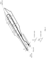
- an embodiment of this application provides an optical add/drop multiplexer, including: a drop signal separator 11 and a drop signal reflector 12.
- the drop signal reflector 12 includes a first transmission mode converter 121, a Bragg grating waveguide 122, and a second transmission mode converter 123.
- a structure of the optical add/drop multiplexer is divided by using dashed lines AA', BB', CC', DD', and EE'.
- the drop signal separator 11 is between AA' and BB'.
- the drop signal reflector 12 is between AA' and EE'.
- the first transmission mode converter 121 is between BB' and CC'.
- the Bragg grating waveguide 122 is between BB' and DD'.
- the second transmission mode converter 123 is between BB' and EE'.
- the drop signal separator 11 is connected to a main input end and a drop end; the drop signal separator 11 is connected to the drop signal reflector 12, and the drop signal reflector 12 is connected to a main output end main output.
- An input end of the drop signal separator 11 is configured to receive optical signals that are in a first mode, and transfer the optical signals that are in the first mode to the drop signal reflector 12 in a single-layer waveguide transmission mode.
- the drop signal reflector 12 is configured to reflect an optical signal that has a predetermined wavelength and that is of the optical signals that are in the first mode to the drop signal separator 11 in a second mode, and output the optical signal from the drop end drop.
- the drop signal reflector 12 is further configured to output, by using the main output end main output, another optical signal of the optical signals that are in the first mode except the optical signal having the predetermined wavelength.
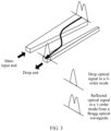
- the drop signal separator 11 includes a first waveguide 111 and a second waveguide 112. An input end of the first waveguide 111 and an output end of the second waveguide 112 are on a same plane, and an output end of the first waveguide 111 and an input end of the second waveguide 112 are on a same plane.
- a width of the first waveguide 111 at the input end is equal to a width of the second waveguide 112 at the output end, a width of the first waveguide 111 linearly increases from the input end to the output end, a width of the second waveguide 112 linearly decreases from the output end to the input end, the input end of the first waveguide 111 is used as a main input end mian input of the drop signal separator 11, and the output end of the second waveguide 112 is used as a drop end drop of the drop signal separator 11.
- the drop signal separator 11 includes two waveguides that are placed in a signal propagation direction and whose widths inversely change.
- the width of the first waveguide 111 increases, and the width of the second waveguide 112 decreases.
- the two waveguides have a same width on an AA' plane, and both meet a single-mode waveguide condition in the silicon optical field.
- the two waveguides have a same length, and a spacing is relatively small, so that optical coupling between predetermined modes can be met.
- the optical signals in the first mode from the outside first enters, from AA', a left-side port (that is, the main input end main input) of the first waveguide 111, and are propagated along the first waveguide 111.
- a modal refractive index for the input optical signal that is in the first mode increases as a waveguide width increases in a propagation process
- the modal refractive index for the optical signal transmitted in the first waveguide 111 continuously increases.
- a modal refractive index of the adjacent second waveguide continuously decreases. Therefore, modal refractive indexes of the two waveguides are not equal at any propagation location of the two waveguides. In other words, a phase matching condition of mode coupling is not met. Therefore, the input optical signal that is in the first mode directly passes the first waveguide 111, and is not coupled into the adjacent second waveguide 112. Eventually, the optical signal enters the drop signal reflector 12.
- the first waveguide 111 is a strip-shaped waveguide, the optical signal in the first waveguide is transmitted in the single-layer waveguide transmission mode.
- the first transmission mode converter 121 includes a first upper layer waveguide 1211 and a first lower layer waveguide 1212.
- the first upper layer waveguide 1211 is located above the first lower layer waveguide 1212, and the first upper layer waveguide 1211 and the first lower layer waveguide 1212 are connected to the drop signal separator 11.
- the first transmission mode converter 121 is configured to convert, into a double-layer waveguide transmission mode, the single-layer waveguide transmission mode in which the drop signal separator 11 sends the optical signals that are in the first mode.
- the first upper layer waveguide 1211 and the first lower layer waveguide 1212 are connected to the output end of the first waveguide 111.
- the optical signal first passes the first transmission mode converter 121.
- the first transmission mode converter 121 is configured to convert the single-layer waveguide (the first waveguide 111) transmission mode of the optical signal into the double-layer (the first upper layer waveguide 1211 and the first lower layer waveguide 1212) transmission mode.
- a width of an input end of the first upper layer waveguide 1211 is equal to a width of the output end of the first waveguide 111.
- a waveguide width of the first upper layer waveguide 1211 remains constant.
- a width of an input end of the first lower layer waveguide 1212 is equal to the width of the output end of the first waveguide 111, and a width of the first lower layer waveguide 1212 linearly increases from the input end to an output end.
- a sum of a thickness of the first upper layer waveguide 1211 and a thickness of the first lower layer waveguide 1212 is equal to a thickness of the first waveguide 111.
- the first transmission mode converter 121 has a sufficient length. This ensures a very small loss in a mode conversion process, in which 0-order mode output is still kept for 0-order mode input, or 1-order mode output is still kept for 1-order mode input. Then the optical signal continues to enter the Bragg grating waveguide 122.
- the Bragg grating waveguide 122 includes a second upper layer waveguide 1221 and a second lower layer waveguide 1222.
- the second upper layer waveguide 1221 is located above the second lower layer waveguide 1222, and the second lower layer waveguide 1222 is connected to the first lower layer waveguide 1212.
- a width of the second upper layer waveguide 1221 regularly changes with a first width alternating with a second width, to form a Bragg grating.
- the first width is greater than the second width, and the second upper layer waveguide 1221 is connected to the first upper layer waveguide 1211.
- the Bragg grating waveguide 122 is configured to: receive the optical signals that are in the first mode sent by the first transmission mode converter 121; and reflect, to the first transmission mode converter 121 as an optical signal that is in the second mode, an optical signal that has a predetermined wavelength and that is of the optical signals that are in the first mode; and is further configured to send, to the second transmission mode converter 123, another optical signal of the optical signals that are in the first mode except the optical signal having the predetermined wavelength.
- a Bragg reflection condition of the Bragg grating meets that an incident optical signal in the first mode is reflected in the second mode.
- the first mode is a 0-order mode (TE 0 ), and the second mode is a 1-order mode (TE 1 ); or the first mode is a 1-order mode, and the second mode is a 0-order mode.
- a width of an input end of the second upper layer waveguide 1221 is equal to the second width
- a width of an output end of the second upper layer waveguide 1222 is equal to the second width.
- a width of a lower layer waveguide, namely the second lower layer waveguide 1222, of the Bragg grating waveguide 122 is consistent with an end width of a lower layer waveguide, namely the first lower layer waveguide 1212, of the first transmission mode converter 121; a width of an upper layer waveguide, namely the second upper layer waveguide 1221, regularly changes; the smaller second width is the same as an end width of an upper layer waveguide, namely the first upper layer waveguide 1211, of the first transmission mode converter 121; the larger first width is less than the width of the second lower layer waveguide 1222; a width of an output end of the second lower layer waveguide 1222 is equal to a width of an output end of the first lower layer waveguide 1212; and the width of the second lower layer waveguide 1222 is constant, thereby forming the Bragg grating.
- a larger first width size of the second upper layer waveguide 1221 and period selection can enable a forward 0-order mode and a backward 1-order mode to meet the Bragg reflection condition.
- the optical signal that is input in the 0-order mode is reflected in the 1-order mode instead of passing the drop signal reflector 12.
- Bandwidth of a Bragg reflectance spectrum is determined based on a coupling factor of a forward mode and a backward mode in the Bragg grating waveguide 122. Three factors, namely a degree of similarity between the two modes, a grating size, and restriction of a waveguide on light, affect the coupling factor.
- the coupling factor increases.
- mainly Bragg reflection between a forward 0-order mode and a backward 0-order mode is used in a Bragg grating waveguide, and the two modes have a relatively high similarity.
- the two modes have a very low similarity.
- the Bragg grating waveguide uses a double-layer waveguide structure, and the second lower layer waveguide at a lower layer in the double-layer waveguide structure is relatively wide. In other words, there is a relatively large waveguide portion having a high refractive index in the Bragg grating waveguide.
- processing of the optical signal by the Bragg grating waveguide 122 includes two cases. In a first case, a wavelength of the optical signal meets a Bragg reflection condition, and the optical signal is reflected back to the first transmission mode converter 121. In a second case, a wavelength of the optical signal does not meet a Bragg reflection condition, and the optical signal is not reflected, but directly passes the Bragg grating waveguide 122 and enters the second transmission mode converter 123.
- the second transmission mode converter 123 includes a third upper layer waveguide 1231 and a third lower layer waveguide 1232.
- the third upper layer waveguide 1231 is located above the third lower layer waveguide 1232, two ends of the third upper layer waveguide 1231 are respectively connected to the second upper layer waveguide 1221 and the main output end main output, and the third lower layer waveguide 1232 is connected to the second lower layer waveguide 1222.
- the second transmission mode converter 123 is configured to convert a transmission mode of the another optical signal into the single-layer waveguide transmission mode, and output the another optical signal by using the main output end main output.
- a width of an input end of the third upper layer waveguide 1231 is equal to the second width, and a width of the third upper layer waveguide 1231 linearly decreases from the input end to an output end.
- a width of an input end of the third lower layer waveguide 1232 is equal to the width of the output end of the second lower layer waveguide 1222, a width of an output end of the third lower layer waveguide 1232 is equal to a width of the output end of the third upper layer waveguide 1231, and a width of the third lower layer waveguide 1232 linearly decreases from the input end to the output end.
- the first transmission mode converter 121 is further configured to convert the optical signal that is in the second mode into the single-layer waveguide transmission mode and output the optical signal to the drop signal separator 11, and the drop signal separator 11 is further configured to output the optical signal that is in the second mode by using the drop end drop.
- the first transmission mode converter 121 in the first case in which the Bragg grating waveguide 122 processes the optical signal, in other words, when a wavelength of signal light meets the Bragg reflection condition, the optical signal is reflected back to the first upper layer waveguide 1221 of the first transmission mode converter 121 in the 1-order mode.
- an effective refractive index in the 1-order mode is less than an effective refractive index in the 0-order mode. Therefore, at a location (for example, a location a shown in FIG. 4 ), an effective refractive index of the first waveguide 111 in the 1-order mode is the same as an effective refractive index of the second waveguide 112 in the 0-order mode. In short, a phase matching relationship is met.
- the optical signal in the 1-order mode in the first waveguide 111 is slowly coupled into the 0-order mode for the second waveguide 112, and is eventually output from a left-side port (the drop end drop) of the second waveguide 112, to complete a drop function.
- the Bragg grating waveguide 122 processes the optical signal
- the optical signal is not reflected, but directly passes the Bragg grating waveguide 122 in the 0-order mode and enters the second transmission mode converter 123.
- the width of an upper layer waveguide, namely the third upper layer waveguide 1231, of the second transmission mode converter 123 decreases, and a maximum width value is the same as the width of the lower layer waveguide, namely the second lower layer waveguide 1222, of the Bragg grating waveguide 122.
- the width of the third upper layer waveguide 1231 decreases, and a maximum width value is the same as a smaller value (the second width) of the width of the upper layer waveguide, namely the second upper layer waveguide 1221, of the Bragg grating waveguide 122.
- the width of the output end of the third lower layer waveguide 1232 is equal to the width of the output end of the third upper layer waveguide 1231, and both waveguides meet a single-mode condition in a silicon photonics field.
- a role of the second transmission mode converter 123 is to convert the double-layer waveguide (the third upper layer waveguide 1231 and the third lower layer waveguide 1232) transmission mode of the optical signal into the single-layer waveguide transmission mode, so that the optical signal is transmitted on an optical fiber connected to the main output end main output.
- the optical signal passing through the second transmission mode converter 123 is output from the main output end main output at EE'.
- a thickness of the first upper layer waveguide is greater than a thickness of the first lower layer waveguide
- a thickness of the second upper layer waveguide is greater than a thickness of the second lower layer waveguide
- a thickness of the third upper layer waveguide is greater than a thickness of the third lower layer waveguide.
Landscapes
- Physics & Mathematics (AREA)
- General Physics & Mathematics (AREA)
- Optics & Photonics (AREA)
- Engineering & Computer Science (AREA)
- Microelectronics & Electronic Packaging (AREA)
- Computer Networks & Wireless Communication (AREA)
- Signal Processing (AREA)
- Power Engineering (AREA)
- Optical Integrated Circuits (AREA)
Description
- This application relates to the field of optoelectronic technologies, and in particular, to an optical add/drop multiplexer.
- An optical add/drop multiplexer is an important filtering device in an optical network, and emergence of the optical add/drop multiplexer enables the optical network to evolve from a point-to-point network to a complex ring network. Implementation of diverse optoelectronic functional devices benefits from development of a silicon optical technology. The optical add/drop multiplexer (Optical Add-Drop Multiplexer, OADM) based on the silicon optical technology mainly includes a microring and a Bragg grating.
- In a conventional OADM having a single Bragg grating waveguide, as long as incident light meets a Bragg grating condition, the incident light is reflected in the Bragg grating waveguide, and leaves from an input port, thereby implementing a selective drop of a specific wavelength. To separate an input signal and a reflected signal, an external circulator or a Y branch structure usually needs to be used at the input port. The conventional OADM having a Bragg grating waveguide mainly uses a reflection condition of the Bragg grating in a lowest-order mode (for example, a 0-order mode). Bandwidth of a reflectance spectrum of the Bragg grating is determined based on a coupling factor of a forward mode and a backward mode in the Bragg grating waveguide. Three factors, namely a degree of similarity between the two modes, a grating size, and restriction of a waveguide on light, affect the coupling factor. When each of the three factors is relatively large, the coupling factor increases. In the prior art, mainly Bragg reflection between a forward 0-order mode and a backward 0-order mode is used in the Bragg grating waveguide, and the two modes have a relatively high similarity. Because light is restricted in the single Bragg grating waveguide, the waveguide also has very strong restriction on light. Therefore, to implement a proper coupling factor requires a relatively small grating size, and usually the grating size is just tens of nanometers. Consequently, it is difficult to meet a process requirement of a CMOS (Complementary Metal Oxide Semiconductor, complementary metal-oxide-semiconductor) in the silicon optical technology, resulting in a great processing difficulty. Especially for DWDM (Dense Wavelength Division Multiplexing, dense wavelength division multiplexing), a grating size is smaller.
-
JP 2016 024298 A -
WO 2016/179869 A1 discloses a tapered waveguide and silicon-based chip. - Embodiments of this application provide an optical add/drop multiplexer, so that a Bragg grating of a relatively large size is used, thereby reducing a processing difficulty.
- To achieve the foregoing objective, the following technical solutions are used in the embodiments of this application.
- According to the invention an optical add/drop multiplexer is provided, and includes a drop signal separator and a drop signal reflector. The drop signal separator is connected to a main input end and a drop end; the drop signal separator is connected to the drop signal reflector, and the drop signal reflector is connected to a main output end; and an input end of the drop signal separator is configured to receive optical signals that are in a first mode, and transfer the optical signals that are in the first mode to the drop signal reflector in a single-layer waveguide transmission mode. The drop signal reflector includes a first transmission mode converter, a Bragg grating waveguide, and a second transmission mode converter. The first transmission mode converter includes a first upper layer waveguide and a first lower layer waveguide, the first upper layer waveguide is located above the first lower layer waveguide, the first upper layer waveguide and the first lower layer waveguide are connected to the drop signal separator, and the first transmission mode converter is configured to convert, into a double-layer waveguide transmission mode, the single-layer waveguide transmission mode in which the drop signal separator sends the optical signals that are in the first mode. The Bragg grating waveguide includes a second upper layer waveguide and a second lower layer waveguide, the second upper layer waveguide is located above the second lower layer waveguide, and the second lower layer waveguide is connected to the first lower layer waveguide; and a width of the second upper layer waveguide regularly changes with a first width alternating with a second width, to form a Bragg grating, where the first width is greater than the second width, the second upper layer waveguide is connected to the first upper layer waveguide, and the Bragg grating waveguide is configured to: receive the optical signals that are in the first mode and that are sent by the first transmission mode converter; and reflect, to the first transmission mode converter as an optical signal that is in a second mode, an optical signal that has a predetermined wavelength and that is of the optical signals that are in the first mode; and is further configured to send, to the second transmission mode converter, another optical signal of the optical signals that are in the first mode except the optical signal having the predetermined wavelength. The second transmission mode converter includes a third upper layer waveguide and a third lower layer waveguide, the third upper layer waveguide is located above the third lower layer waveguide, two ends of the third upper layer waveguide are respectively connected to the second upper layer waveguide and the main output end, and the third lower layer waveguide is connected to the second lower layer waveguide; and the second transmission mode converter is configured to convert a transmission mode of the another optical signal into the single-layer waveguide transmission mode, and output the another optical signal by using the main output end. The first transmission mode converter is further configured to convert the optical signal that is in the second mode into the single-layer waveguide transmission mode and output the optical signal to the drop signal separator, and the drop signal separator is further configured to output the optical signal that is in the second mode by using the drop end. In the foregoing solution, the drop signal reflector includes a double-layer waveguide structure, and the double-layer waveguide structure reduces restriction on light. Therefore, the Bragg grating can reduce coupling between incident signal light that is in the first mode and reflected signal light that is in the second mode. In this way, to achieve reflectance spectrum bandwidth same as that required in the prior art, a larger grating size can be used, lowering a process requirement.
- In an example, the drop signal separator includes a first waveguide and a second waveguide, an input end of the first waveguide and an output end of the second waveguide are on a same plane, and an output end of the first waveguide and an input end of the second waveguide are on a same plane; and a width of the first waveguide at the input end is equal to a width of the second waveguide at the output end, a width of the first waveguide linearly increases from the input end to the output end, a width of the second waveguide linearly decreases from the output end to the input end, the output end of the first waveguide is connected to the first upper layer waveguide and the first lower layer waveguide, the input end of the first waveguide is used as a main input end of the drop signal separator, and the output end of the second waveguide is used as a drop end of the drop signal separator. In this solution, the width of the first waveguide and the width of the second waveguide inversely change. Consequently, an index of refraction of the optical signal that is in the first mode by the first waveguide and an index of effective refraction of the optical signal that is in the second mode by the second waveguide cross each other. In other words, at a location in the drop signal separator, the index of refraction of the optical signal that is in the first mode by the first waveguide is equal to the index of effective refraction of the optical signal that is in the second mode by the second waveguide. Therefore, the optical signal that is in the second mode can be output from the second waveguide, thereby reducing a loss of separating drop signals.
- In addition, a width of an input end of the first upper layer waveguide is equal to a width of the output end of the first waveguide, and a width of the first upper layer waveguide is equal to the second width; and a width of an input end of the first lower layer waveguide is equal to the width of the output end of the first waveguide, a width of an output end of the first lower layer waveguide is greater than the first width, and a width of the first lower layer waveguide linearly increases from the input end to the output end.
- In an example, a thickness of the first upper layer waveguide is greater than a thickness of the first lower layer waveguide.
- In an example, a width of an input end of the second upper layer waveguide is equal to the second width, and a width of an output end of the second upper layer waveguide is equal to the second width; and a width of an input end of the second lower layer waveguide is equal to a width of an output end of the first lower layer waveguide, a width of an output end of the second lower layer waveguide is equal to the width of the output end of the first lower layer waveguide, and a width of the second lower layer waveguide is constant.
- In an example, a thickness of the second upper layer waveguide is greater than a thickness of the second lower layer waveguide.
- In an example, a width of an input end of the third upper layer waveguide is equal to the second width, and a width of the third upper layer waveguide linearly decreases from the input end to an output end; and a width of an input end of the third lower layer waveguide is equal to a width of an output end of the second lower layer waveguide, a width of an output end of the third lower layer waveguide is equal to a width of the output end of the third upper layer waveguide, and a width of the third lower layer waveguide linearly decreases from the input end to the output end.
- In an example, a thickness of the third upper layer waveguide is greater than a thickness of the third lower layer waveguide.
- In an example, the first upper layer waveguide, the second upper layer waveguide, and the third upper layer waveguide are identical in thickness; and the first lower layer waveguide, the second lower layer waveguide, and the third lower layer waveguide are identical in thickness.
- In an example, the first mode is a 0-order mode, and the second mode is a 1-order mode; or the first mode is a 1-order mode, and the second mode is a 0-order mode.
- To describe the technical solutions in the embodiments of this application or in the prior art more clearly, the following briefly describes the accompanying drawings required for describing the embodiments or the prior art.
-
FIG. 1 is a schematic structural diagram of an optical add/drop multiplexer according to an embodiment of this application; -
FIG. 2 is a schematic structural diagram of an optical add/drop multiplexer according to another embodiment of this application; -
FIG. 3 is a schematic structural diagram of a drop signal separator according to an embodiment of this application; -
FIG. 4 is a schematic diagram of an index of refraction of an optical signal in each mode by each waveguide in a drop signal separator according to an embodiment of this application; and -
FIG. 5 is a schematic diagram of simulation of a flare of an optical signal in a drop signal separator according to an embodiment of this application. - The following describes the embodiments of this application with reference to accompanying drawings.
- An optical add/drop multiplexer provided in the embodiments of this application is applied to an optical network that uses an optical fiber as a main transmission medium, such as a wide area network, a metropolitan area network, a newly established local area network with a large coverage. The optical add/drop multiplexer is mainly applied to a node that is in the optical network and that needs to upload and download a signal with a specific wavelength.
- As shown in
FIG. 1 andFIG. 2 , an embodiment of this application provides an optical add/drop multiplexer, including:
adrop signal separator 11 and adrop signal reflector 12. Thedrop signal reflector 12 includes a firsttransmission mode converter 121, a Bragggrating waveguide 122, and a secondtransmission mode converter 123. As shown inFIG. 1 , a structure of the optical add/drop multiplexer is divided by using dashed lines AA', BB', CC', DD', and EE'. Thedrop signal separator 11 is between AA' and BB'. Thedrop signal reflector 12 is between AA' and EE'. The firsttransmission mode converter 121 is between BB' and CC'. The Bragggrating waveguide 122 is between BB' and DD'. The secondtransmission mode converter 123 is between BB' and EE'. As shown inFIG. 2 , thedrop signal separator 11 is connected to a main input end and a drop end; thedrop signal separator 11 is connected to thedrop signal reflector 12, and thedrop signal reflector 12 is connected to a main output end main output. An input end of thedrop signal separator 11 is configured to receive optical signals that are in a first mode, and transfer the optical signals that are in the first mode to thedrop signal reflector 12 in a single-layer waveguide transmission mode. Thedrop signal reflector 12 is configured to reflect an optical signal that has a predetermined wavelength and that is of the optical signals that are in the first mode to thedrop signal separator 11 in a second mode, and output the optical signal from the drop end drop. Thedrop signal reflector 12 is further configured to output, by using the main output end main output, another optical signal of the optical signals that are in the first mode except the optical signal having the predetermined wavelength. - For example, the
drop signal separator 11 includes afirst waveguide 111 and asecond waveguide 112. An input end of thefirst waveguide 111 and an output end of thesecond waveguide 112 are on a same plane, and an output end of thefirst waveguide 111 and an input end of thesecond waveguide 112 are on a same plane. A width of thefirst waveguide 111 at the input end is equal to a width of thesecond waveguide 112 at the output end, a width of thefirst waveguide 111 linearly increases from the input end to the output end, a width of thesecond waveguide 112 linearly decreases from the output end to the input end, the input end of thefirst waveguide 111 is used as a main input end mian input of thedrop signal separator 11, and the output end of thesecond waveguide 112 is used as a drop end drop of thedrop signal separator 11. Herein, thedrop signal separator 11 includes two waveguides that are placed in a signal propagation direction and whose widths inversely change. In the same direction, the width of thefirst waveguide 111 increases, and the width of thesecond waveguide 112 decreases. The two waveguides have a same width on an AA' plane, and both meet a single-mode waveguide condition in the silicon optical field. The two waveguides have a same length, and a spacing is relatively small, so that optical coupling between predetermined modes can be met. The optical signals in the first mode from the outside first enters, from AA', a left-side port (that is, the main input end main input) of thefirst waveguide 111, and are propagated along thefirst waveguide 111. Because a modal refractive index for the input optical signal that is in the first mode increases as a waveguide width increases in a propagation process, the modal refractive index for the optical signal transmitted in thefirst waveguide 111 continuously increases. However, a modal refractive index of the adjacent second waveguide continuously decreases. Therefore, modal refractive indexes of the two waveguides are not equal at any propagation location of the two waveguides. In other words, a phase matching condition of mode coupling is not met. Therefore, the input optical signal that is in the first mode directly passes thefirst waveguide 111, and is not coupled into the adjacentsecond waveguide 112. Eventually, the optical signal enters thedrop signal reflector 12. In addition, because thefirst waveguide 111 is a strip-shaped waveguide, the optical signal in the first waveguide is transmitted in the single-layer waveguide transmission mode. - As shown in
FIG. 1 andFIG. 2 , the firsttransmission mode converter 121 includes a firstupper layer waveguide 1211 and a firstlower layer waveguide 1212. The firstupper layer waveguide 1211 is located above the firstlower layer waveguide 1212, and the firstupper layer waveguide 1211 and the firstlower layer waveguide 1212 are connected to thedrop signal separator 11. The firsttransmission mode converter 121 is configured to convert, into a double-layer waveguide transmission mode, the single-layer waveguide transmission mode in which thedrop signal separator 11 sends the optical signals that are in the first mode. Specifically, the firstupper layer waveguide 1211 and the firstlower layer waveguide 1212 are connected to the output end of thefirst waveguide 111. - For example, after the optical signal enters the
drop signal reflector 12, the optical signal first passes the firsttransmission mode converter 121. The firsttransmission mode converter 121 is configured to convert the single-layer waveguide (the first waveguide 111) transmission mode of the optical signal into the double-layer (the firstupper layer waveguide 1211 and the first lower layer waveguide 1212) transmission mode. A width of an input end of the firstupper layer waveguide 1211 is equal to a width of the output end of thefirst waveguide 111. A waveguide width of the firstupper layer waveguide 1211 remains constant. A width of an input end of the firstlower layer waveguide 1212 is equal to the width of the output end of thefirst waveguide 111, and a width of the firstlower layer waveguide 1212 linearly increases from the input end to an output end. In addition, a sum of a thickness of the firstupper layer waveguide 1211 and a thickness of the firstlower layer waveguide 1212 is equal to a thickness of thefirst waveguide 111. The firsttransmission mode converter 121 has a sufficient length. This ensures a very small loss in a mode conversion process, in which 0-order mode output is still kept for 0-order mode input, or 1-order mode output is still kept for 1-order mode input. Then the optical signal continues to enter theBragg grating waveguide 122. - The
Bragg grating waveguide 122 includes a secondupper layer waveguide 1221 and a secondlower layer waveguide 1222. The secondupper layer waveguide 1221 is located above the secondlower layer waveguide 1222, and the secondlower layer waveguide 1222 is connected to the firstlower layer waveguide 1212. A width of the secondupper layer waveguide 1221 regularly changes with a first width alternating with a second width, to form a Bragg grating. The first width is greater than the second width, and the secondupper layer waveguide 1221 is connected to the firstupper layer waveguide 1211. TheBragg grating waveguide 122 is configured to: receive the optical signals that are in the first mode sent by the firsttransmission mode converter 121; and reflect, to the firsttransmission mode converter 121 as an optical signal that is in the second mode, an optical signal that has a predetermined wavelength and that is of the optical signals that are in the first mode; and is further configured to send, to the secondtransmission mode converter 123, another optical signal of the optical signals that are in the first mode except the optical signal having the predetermined wavelength. - A Bragg reflection condition of the Bragg grating meets that an incident optical signal in the first mode is reflected in the second mode. The first mode is a 0-order mode (TE0), and the second mode is a 1-order mode (TE1); or the first mode is a 1-order mode, and the second mode is a 0-order mode. For example, a width of an input end of the second
upper layer waveguide 1221 is equal to the second width, and a width of an output end of the secondupper layer waveguide 1222 is equal to the second width. A width of a lower layer waveguide, namely the secondlower layer waveguide 1222, of theBragg grating waveguide 122 is consistent with an end width of a lower layer waveguide, namely the firstlower layer waveguide 1212, of the firsttransmission mode converter 121; a width of an upper layer waveguide, namely the secondupper layer waveguide 1221, regularly changes; the smaller second width is the same as an end width of an upper layer waveguide, namely the firstupper layer waveguide 1211, of the firsttransmission mode converter 121; the larger first width is less than the width of the secondlower layer waveguide 1222; a width of an output end of the secondlower layer waveguide 1222 is equal to a width of an output end of the firstlower layer waveguide 1212; and the width of the secondlower layer waveguide 1222 is constant, thereby forming the Bragg grating. For example, if an optical signal of the main input end main input is in the 0-order mode, a larger first width size of the secondupper layer waveguide 1221 and period selection can enable a forward 0-order mode and a backward 1-order mode to meet the Bragg reflection condition. In other words, the optical signal that is input in the 0-order mode is reflected in the 1-order mode instead of passing thedrop signal reflector 12. Bandwidth of a Bragg reflectance spectrum is determined based on a coupling factor of a forward mode and a backward mode in theBragg grating waveguide 122. Three factors, namely a degree of similarity between the two modes, a grating size, and restriction of a waveguide on light, affect the coupling factor. When each of the three factors is relatively large, the coupling factor increases. In the prior art, mainly Bragg reflection between a forward 0-order mode and a backward 0-order mode is used in a Bragg grating waveguide, and the two modes have a relatively high similarity. However, in reflection between the 0-order mode and the 1-order mode that is used in the present invention, the two modes have a very low similarity. In addition, the Bragg grating waveguide uses a double-layer waveguide structure, and the second lower layer waveguide at a lower layer in the double-layer waveguide structure is relatively wide. In other words, there is a relatively large waveguide portion having a high refractive index in the Bragg grating waveguide. Restriction of the waveguide portion on light is relatively weak, thereby further reducing restriction of the waveguide on light. Therefore, when Bragg reflection having a same degree as that in the prior art is considered, in other words, when the coupling factors are the same, the prior art requires a relatively small grating size, but this application requires a relatively large grating size, so that a process requirement of a device is relatively low. In addition, based on a wavelength of signal light, processing of the optical signal by theBragg grating waveguide 122 includes two cases. In a first case, a wavelength of the optical signal meets a Bragg reflection condition, and the optical signal is reflected back to the firsttransmission mode converter 121. In a second case, a wavelength of the optical signal does not meet a Bragg reflection condition, and the optical signal is not reflected, but directly passes theBragg grating waveguide 122 and enters the secondtransmission mode converter 123. - As shown in
FIG. 1 andFIG. 2 , the secondtransmission mode converter 123 includes a thirdupper layer waveguide 1231 and a thirdlower layer waveguide 1232. The thirdupper layer waveguide 1231 is located above the thirdlower layer waveguide 1232, two ends of the thirdupper layer waveguide 1231 are respectively connected to the secondupper layer waveguide 1221 and the main output end main output, and the thirdlower layer waveguide 1232 is connected to the secondlower layer waveguide 1222. The secondtransmission mode converter 123 is configured to convert a transmission mode of the another optical signal into the single-layer waveguide transmission mode, and output the another optical signal by using the main output end main output. - A width of an input end of the third
upper layer waveguide 1231 is equal to the second width, and a width of the thirdupper layer waveguide 1231 linearly decreases from the input end to an output end. A width of an input end of the thirdlower layer waveguide 1232 is equal to the width of the output end of the secondlower layer waveguide 1222, a width of an output end of the thirdlower layer waveguide 1232 is equal to a width of the output end of the thirdupper layer waveguide 1231, and a width of the thirdlower layer waveguide 1232 linearly decreases from the input end to the output end. - Further, the first
transmission mode converter 121 is further configured to convert the optical signal that is in the second mode into the single-layer waveguide transmission mode and output the optical signal to thedrop signal separator 11, and thedrop signal separator 11 is further configured to output the optical signal that is in the second mode by using the drop end drop. Specifically, as shown inFIG. 3 ,FIG. 4 , andFIG. 5 , in the first case in which theBragg grating waveguide 122 processes the optical signal, in other words, when a wavelength of signal light meets the Bragg reflection condition, the optical signal is reflected back to the firstupper layer waveguide 1221 of the firsttransmission mode converter 121 in the 1-order mode. In this case, in a light propagation direction, a waveguide width of thefirst waveguide 111 decreases, and a width of thesecond waveguide 112 increases. However, with a same waveguide width, an effective refractive index in the 1-order mode is less than an effective refractive index in the 0-order mode. Therefore, at a location (for example, a location a shown inFIG. 4 ), an effective refractive index of thefirst waveguide 111 in the 1-order mode is the same as an effective refractive index of thesecond waveguide 112 in the 0-order mode. In short, a phase matching relationship is met. Therefore, the optical signal in the 1-order mode in thefirst waveguide 111 is slowly coupled into the 0-order mode for thesecond waveguide 112, and is eventually output from a left-side port (the drop end drop) of thesecond waveguide 112, to complete a drop function. - In the second case in which the
Bragg grating waveguide 122 processes the optical signal, in other words, when a wavelength of the optical signal does not meet the Bragg reflection condition, the optical signal is not reflected, but directly passes theBragg grating waveguide 122 in the 0-order mode and enters the secondtransmission mode converter 123. The width of an upper layer waveguide, namely the thirdupper layer waveguide 1231, of the secondtransmission mode converter 123 decreases, and a maximum width value is the same as the width of the lower layer waveguide, namely the secondlower layer waveguide 1222, of theBragg grating waveguide 122. The width of the thirdupper layer waveguide 1231 decreases, and a maximum width value is the same as a smaller value (the second width) of the width of the upper layer waveguide, namely the secondupper layer waveguide 1221, of theBragg grating waveguide 122. The width of the output end of the thirdlower layer waveguide 1232 is equal to the width of the output end of the thirdupper layer waveguide 1231, and both waveguides meet a single-mode condition in a silicon photonics field. A role of the secondtransmission mode converter 123 is to convert the double-layer waveguide (the thirdupper layer waveguide 1231 and the third lower layer waveguide 1232) transmission mode of the optical signal into the single-layer waveguide transmission mode, so that the optical signal is transmitted on an optical fiber connected to the main output end main output. The optical signal passing through the secondtransmission mode converter 123 is output from the main output end main output at EE'. - In addition, a thickness of the first upper layer waveguide is greater than a thickness of the first lower layer waveguide, a thickness of the second upper layer waveguide is greater than a thickness of the second lower layer waveguide, and a thickness of the third upper layer waveguide is greater than a thickness of the third lower layer waveguide. The first upper layer waveguide, the second upper layer waveguide, and the third upper layer waveguide are identical in thickness; the first lower layer waveguide, the second lower layer waveguide, and the third lower layer waveguide are identical in thickness.
- Although this application is described with reference to the embodiments, in a process of implementing this application that claims protection, a person skilled in the art may understand and implement another variation of the disclosed embodiments by viewing the accompanying drawings, disclosed content, and the accompanying claims. In the claims, "comprising" (comprising) does not exclude another component or another step, and "a" or "one" does not exclude a case of multiple. Some measures are recorded in dependent claims that are different from each other, but this does not mean that these measures cannot be combined to produce a better effect.
- Although this application is described with reference to specific features and the embodiments thereof, apparently, various modifications and combinations may be made to them without departing from the scope of this application. Correspondingly, the specification and accompanying drawings are merely example descriptions of this application defined by the accompanying claims. Apparently, a person skilled in the art can make various modifications and variations to this application without departing from the scope of this application. This application is intended to cover these modifications and variations provided that they fall within the scope of protection defined by the claims of this application.
Claims (10)
- An optical add/drop multiplexer, comprising a drop signal separator (11) and a drop signal reflector (12), whereinthe drop signal separator (11) is connected to a main input end and a drop end; the drop signal separator is connected to the drop signal reflector, and the drop signal reflector is connected to a main output end; and an input end of the drop signal separator is configured to receive optical signals that are in a first mode and transfer the optical signals that are in the first mode to the drop signal reflector in a single-layer waveguide transmission mode;the drop signal reflector (12) comprises a first transmission mode converter (121), a Bragg grating waveguide (122), and a second transmission mode converter (123);the first transmission mode converter (121) comprises a first upper layer waveguide (1211) and a first lower layer waveguide (1212), the first upper layer waveguide (1211) is located above the first lower layer waveguide (1212), the first upper layer waveguide (1211) and the first lower layer waveguide (1212) are connected to the drop signal separator (11), and the first transmission mode converter (121) is configured to convert, into a double-layer waveguide transmission mode, the single-layer waveguide transmission mode in which the drop signal separator (11) sends the optical signals that are in the first mode;the Bragg grating waveguide (122) comprises a second upper layer (1221) waveguide and a second lower layer waveguide (1222), the second upper layer waveguide (1221) is located above the second lower layer waveguide (1222), and the second lower layer waveguide (1222) is connected to the first lower layer waveguide (1212); and a width of the second upper layer waveguide (1221) regularly changes with a first width alternating with a second width, to form a Bragg grating, wherein the first width is greater than the second width, the second upper layer waveguide (1221) is connected to the first upper layer waveguide (1211), and the Bragg grating waveguide is configured to: receive the optical signals that are in the first mode and that are sent by the first transmission mode converter (121); and reflect, to the first transmission mode converter (121) as an optical signal that is in a second mode, an optical signal that has a predetermined wavelength and that is of the optical signals that are in the first mode; and is further configured to send, to the second transmission mode converter (123), another optical signal of the optical signals that are in the first mode except the optical signal having the predetermined wavelength;the second transmission mode converter (123) comprises a third upper layer waveguide (1231) and a third lower layer waveguide (1232), the third upper layer waveguide (1231) is located above the third lower layer waveguide (1232), two ends of the third upper layer waveguide (1231) are respectively connected to the second upper layer waveguide (1221) and the main output end, and the third lower layer waveguide (1232) is connected to the second lower layer waveguide (1222); and the second transmission mode converter (123) is configured to convert a transmission mode of the another optical signal into the single-layer waveguide transmission mode, and output the another optical signal by using the main output end; andthe first transmission mode converter (121) is further configured to convert the optical signal that is in the second mode into the single-layer waveguide transmission mode and output the optical signal to the drop signal separator (11), and the drop signal separator (11) is further configured to output the optical signal that is in the second mode by using the drop end.
- The optical add/drop multiplexer according to claim 1, wherein the drop signal separator (11) comprises a first waveguide (111) and a second waveguide (112), an input end of the first waveguide (111) and an output end of the second waveguide (112) are on a same plane, and an output end of the first waveguide (111) and an input end of the second waveguide (112) are on a same plane; and a width of the first waveguide (111) at the input end is equal to a width of the second waveguide (112) at the output end, a width of the first waveguide (111) linearly increases from the input end to the output end, a width of the second waveguide (112) linearly decreases from the output end to the input end, the output end of the first waveguide (111) is connected to the first upper layer waveguide (1211) and the first lower layer waveguide (1212), the input end of the first waveguide (111) is used as a main input end of the drop signal separator (11), and the output end of the second waveguide (112) is used as a drop end of the drop signal separator (11).
- The optical add/drop multiplexer according to claim 2, wherein a width of an input end of the first upper layer waveguide (1211) is equal to a width of the output end of the first waveguide (111), and a width of the first upper layer waveguide (1211) is equal to the second width; and
a width of an input end of the first lower layer waveguide (1212) is equal to the width of the output end of the first waveguide (111), a width of an output end of the first lower layer waveguide (1212) is greater than the first width, and a width of the first lower layer waveguide (1212) linearly increases from the input end to the output end. - The optical add/drop multiplexer according to claim 1, wherein a thickness of the first upper layer waveguide (1211) is greater than a thickness of the first lower layer waveguide (1212).
- The optical add/drop multiplexer according to claim 1, wherein a width of an input end of the second upper layer waveguide (1221) is equal to the second width, and a width of an output end of the second upper layer waveguide (1221) is equal to the second width; and
a width of an input end of the second lower layer waveguide (1222) is equal to a width of an output end of the first lower layer waveguide (1212), a width of an output end of the second lower layer waveguide (1222) is equal to the width of the output end of the first lower layer waveguide (1212), and a width of the second lower layer waveguide (1222) is constant. - The optical add/drop multiplexer according to claim 1, wherein a thickness of the second upper layer waveguide (1221) is greater than a thickness of the second lower layer waveguide (1222).
- The optical add/drop multiplexer according to claim 1, wherein a width of an input end of the third upper layer waveguide (1231) is equal to the second width, and a width of the third upper layer waveguide (1231) linearly decreases from the input end to an output end; and
a width of an input end of the third lower layer waveguide (1232) is equal to a width of an output end of the second lower layer waveguide (1222), a width of an output end of the third lower layer waveguide (1232) is equal to a width of the output end of the third upper layer waveguide (1231), and a width of the third lower layer waveguide (1232) linearly decreases from the input end to the output end. - The optical add/drop multiplexer according to claim 1, wherein a thickness of the third upper layer waveguide (1231) is greater than a thickness of the third lower layer waveguide (1232).
- The optical add/drop multiplexer according to claim 1, wherein the first upper layer waveguide (1211), the second upper layer waveguide (1221), and the third upper layer waveguide (1231) are identical in thickness; and
the first lower layer waveguide (1212), the second lower layer waveguide (1222), and the third lower layer waveguide (1232) are identical in thickness. - The optical add/drop multiplexer according to claim 1, wherein the first mode is a 0-order mode, and the second mode is a 1-order mode; or the first mode is a 1-order mode, and the second mode is a 0-order mode.
Applications Claiming Priority (1)
| Application Number | Priority Date | Filing Date | Title |
|---|---|---|---|
| PCT/CN2017/088661 WO2018227556A1 (en) | 2017-06-16 | 2017-06-16 | Optical add-drop multiplexer |
Publications (3)
| Publication Number | Publication Date |
|---|---|
| EP3629068A1 EP3629068A1 (en) | 2020-04-01 |
| EP3629068A4 EP3629068A4 (en) | 2020-06-03 |
| EP3629068B1 true EP3629068B1 (en) | 2024-10-30 |
Family
ID=64660505
Family Applications (1)
| Application Number | Title | Priority Date | Filing Date |
|---|---|---|---|
| EP17913833.4A Active EP3629068B1 (en) | 2017-06-16 | 2017-06-16 | Optical add-drop multiplexer |
Country Status (4)
| Country | Link |
|---|---|
| US (1) | US10871615B2 (en) |
| EP (1) | EP3629068B1 (en) |
| CN (1) | CN110637245B (en) |
| WO (1) | WO2018227556A1 (en) |
Families Citing this family (4)
| Publication number | Priority date | Publication date | Assignee | Title |
|---|---|---|---|---|
| CN112630995B (en) * | 2021-01-11 | 2022-06-17 | 东南大学 | Method for converting polarization state of optical signal by silicon-based polarization rotator |
| GB2625806A (en) * | 2022-12-23 | 2024-07-03 | Light Trace Photonics Ltd | Housing for accommodating a photonic integrated circuit chip |
| US12372722B2 (en) | 2023-01-12 | 2025-07-29 | Cisco Technology, Inc. | Multimode waveguide with adiabatic TE0 mode add/drop filter |
| US12395263B2 (en) * | 2023-01-12 | 2025-08-19 | Cisco Technology, Inc. | Wavelength division multiplexing architecture based on integrated bragg and adiabatic TE0 mode add/drop filter |
Family Cites Families (27)
| Publication number | Priority date | Publication date | Assignee | Title |
|---|---|---|---|---|
| JPH08237203A (en) * | 1995-02-23 | 1996-09-13 | Fujitsu Ltd | Optical filter array, optical transmitter and optical transmission system |
| US6047096A (en) | 1997-03-07 | 2000-04-04 | Telefonaktiebolaget Lm Ericsson | Optical device |
| SE516534C2 (en) | 2000-06-05 | 2002-01-29 | Ericsson Telefon Ab L M | Bragg grid assisted MMIMI coupler for adjustable add / drop multiplexing |
| US7245792B2 (en) | 2002-08-16 | 2007-07-17 | Intel Corporation | Silicon-based tunable single passband optical filter |
| US7126749B2 (en) * | 2002-12-20 | 2006-10-24 | Quantum Photonics, Inc. | Semiconductor optical amplifier with low polarization gain dependency |
| WO2006007868A1 (en) * | 2004-07-22 | 2006-01-26 | Pirelli & C. S.P.A. | Integrated wavelength selective grating-based filter |
| CN1845484B (en) | 2005-04-08 | 2010-12-29 | 中国科学院半导体研究所 | Realize the structure and manufacturing method of reconfigurable optical add-drop multiplexer |
| US7283709B2 (en) | 2005-10-06 | 2007-10-16 | Lucent Technologies Inc. | Integrated microelectromechanical wavelength selective switch and method of making same |
| CN1764096A (en) * | 2005-10-26 | 2006-04-26 | 中山大学 | An Optical Add-Drop Multiplexer with Adjustable Upper and Lower Wavelength Channels |
| US7639911B2 (en) * | 2005-12-08 | 2009-12-29 | Electronics And Telecommunications Research Institute | Optical device having optical waveguide including organic Bragg grating sheet |
| JP2010510548A (en) | 2006-11-21 | 2010-04-02 | ワンチップ フォトニクス インコーポレイテッド | Integrated optical element array for wavelength (inverse) multiplexing using multi-waveguide vertical stacking |
| JP4500886B2 (en) * | 2008-02-29 | 2010-07-14 | 株式会社フジクラ | Optical waveguide device, chromatic dispersion compensation device and design method thereof, optical filter and design method thereof, and optical resonator and design method thereof |
| CN101672987B (en) * | 2008-09-12 | 2013-01-02 | 华为技术有限公司 | Optical isolator, optical add/drop multiplexer and optical combiner |
| US8098969B2 (en) * | 2009-12-08 | 2012-01-17 | Onechip Photonics Inc. | Waveguide optically pre-amplified detector with passband wavelength filtering |
| TWI415411B (en) | 2011-01-20 | 2013-11-11 | Univ Nat Central | Single stage 1 × 5 grating auxiliary wavelength multiplex structure |
| CN102879858B (en) * | 2012-10-26 | 2015-05-13 | 江苏尚飞光电科技有限公司 | Single-fiber three-way multiplexer with grating |
| US8948549B2 (en) * | 2012-11-27 | 2015-02-03 | Teraxion Inc. | Polarization rotator assembly including a subwavelength composite portion |
| CN103217738B (en) * | 2013-03-27 | 2015-05-13 | 浙江大学 | Mode add-drop multiplexing and demultiplexing device based on grating-assisting type coupler |
| CN103197387B (en) * | 2013-04-11 | 2015-10-07 | 浙江工业大学 | Based on the optical add/drop multiplexer of Preset grating long-period waveguide grating |
| JP6194789B2 (en) * | 2013-12-24 | 2017-09-13 | 沖電気工業株式会社 | Optical waveguide device |
| JP6402519B2 (en) * | 2014-07-18 | 2018-10-10 | 沖電気工業株式会社 | Optical waveguide device |
| CN107924024B (en) * | 2015-05-08 | 2020-10-16 | 华为技术有限公司 | Tapered waveguide and silicon-based chip |
| JP6089077B1 (en) * | 2015-08-25 | 2017-03-01 | 沖電気工業株式会社 | Waveguide type optical diffraction grating and optical wavelength filter |
| US9989702B2 (en) * | 2015-11-24 | 2018-06-05 | International Business Machines Corporation | Polarization rotator for silicon photonics |
| CN105866893B (en) * | 2016-06-08 | 2019-01-15 | 龙岩学院 | A kind of optical add/drop multiplexer based on antisymmetry multimode Bragg waveguide grating |
| US10228512B2 (en) * | 2016-09-29 | 2019-03-12 | Oki Electric Industry Co., Ltd. | Wavelength filter |
| JP6379245B1 (en) * | 2017-03-16 | 2018-08-22 | 沖電気工業株式会社 | Optical waveguide device and receiving circuit |
-
2017
- 2017-06-16 WO PCT/CN2017/088661 patent/WO2018227556A1/en not_active Ceased
- 2017-06-16 CN CN201780090991.9A patent/CN110637245B/en active Active
- 2017-06-16 EP EP17913833.4A patent/EP3629068B1/en active Active
-
2019
- 2019-12-16 US US16/715,958 patent/US10871615B2/en active Active
Also Published As
| Publication number | Publication date |
|---|---|
| WO2018227556A1 (en) | 2018-12-20 |
| US20200116939A1 (en) | 2020-04-16 |
| CN110637245B (en) | 2020-12-01 |
| EP3629068A1 (en) | 2020-04-01 |
| CN110637245A (en) | 2019-12-31 |
| EP3629068A4 (en) | 2020-06-03 |
| US10871615B2 (en) | 2020-12-22 |
Similar Documents
| Publication | Publication Date | Title |
|---|---|---|
| US10871615B2 (en) | Optical add/drop multiplexer | |
| CN106249355B (en) | Mode multiplexing and demultiplexer based on silicon-based optical waveguide mode matching | |
| CN107422421B (en) | A sparse wavelength division multiplexer based on curved directional couplers | |
| EP3208960B1 (en) | Mode converter | |
| EP3203281B1 (en) | Mode multiplexer-demultiplexer and switching node | |
| CN104459881A (en) | Wavelength division multiplexing type silicon substrate optical receiving chip insensitive to polarization | |
| CN104918145B (en) | Single-chip integration formula multi-wavelength palarization multiplexing/demultiplexer | |
| EP3499282B1 (en) | Polarization independent optical device | |
| CN114641720A (en) | Polarization system and method | |
| Guan et al. | High-efficiency biwavelength polarization splitter-rotator on the SOI platform | |
| Shi et al. | Silicon CWDM demultiplexers using contra-directional couplers | |
| CN108833016B (en) | Single-chip integrated wavelength division multiplexing single-fiber bidirectional data transmission module | |
| US20190158190A1 (en) | Optical receiver module and operation method thereof | |
| CN109541753B (en) | A flattening filter and a Mux and Demux filter composed of the same | |
| US8406579B2 (en) | Wavelength division multiplexing and optical modulation apparatus | |
| TWI415411B (en) | Single stage 1 × 5 grating auxiliary wavelength multiplex structure | |
| JP6302375B2 (en) | Optical receiver | |
| CN104965260B (en) | There is the optical resonantor of reflection in a kind of coupler | |
| JP6312198B2 (en) | Optical multiplexing device and optical demultiplexing device | |
| JPS5815926Y2 (en) | Composite optical wavelength demultiplexing circuit | |
| JP2015059982A (en) | Optical waveguide device and method of manufacturing the same | |
| KR20210023511A (en) | Wavelength demultiplexer with arrayed waveguide grating and methods of manufacturing | |
| JP7830306B2 (en) | Optical integrated circuits and optical transceivers | |
| CN103048809B (en) | Delay adjustable device based on active fiber grating coupler | |
| Ankiewicz et al. | Narrow bandpass filter using Bragg grating coupler in transmission mode |
Legal Events
| Date | Code | Title | Description |
|---|---|---|---|
| STAA | Information on the status of an ep patent application or granted ep patent |
Free format text: STATUS: THE INTERNATIONAL PUBLICATION HAS BEEN MADE |
|
| PUAI | Public reference made under article 153(3) epc to a published international application that has entered the european phase |
Free format text: ORIGINAL CODE: 0009012 |
|
| STAA | Information on the status of an ep patent application or granted ep patent |
Free format text: STATUS: REQUEST FOR EXAMINATION WAS MADE |
|
| 17P | Request for examination filed |
Effective date: 20191223 |
|
| AK | Designated contracting states |
Kind code of ref document: A1 Designated state(s): AL AT BE BG CH CY CZ DE DK EE ES FI FR GB GR HR HU IE IS IT LI LT LU LV MC MK MT NL NO PL PT RO RS SE SI SK SM TR |
|
| AX | Request for extension of the european patent |
Extension state: BA ME |
|
| A4 | Supplementary search report drawn up and despatched |
Effective date: 20200508 |
|
| RIC1 | Information provided on ipc code assigned before grant |
Ipc: G02B 6/122 20060101ALI20200501BHEP Ipc: G02B 6/12 20060101ALI20200501BHEP Ipc: G02B 6/124 20060101ALI20200501BHEP Ipc: H04J 14/02 20060101ALI20200501BHEP Ipc: G02B 6/293 20060101AFI20200501BHEP |
|
| DAV | Request for validation of the european patent (deleted) | ||
| DAX | Request for extension of the european patent (deleted) | ||
| STAA | Information on the status of an ep patent application or granted ep patent |
Free format text: STATUS: EXAMINATION IS IN PROGRESS |
|
| 17Q | First examination report despatched |
Effective date: 20221111 |
|
| GRAP | Despatch of communication of intention to grant a patent |
Free format text: ORIGINAL CODE: EPIDOSNIGR1 |
|
| STAA | Information on the status of an ep patent application or granted ep patent |
Free format text: STATUS: GRANT OF PATENT IS INTENDED |
|
| INTG | Intention to grant announced |
Effective date: 20240610 |
|
| GRAS | Grant fee paid |
Free format text: ORIGINAL CODE: EPIDOSNIGR3 |
|
| GRAA | (expected) grant |
Free format text: ORIGINAL CODE: 0009210 |
|
| STAA | Information on the status of an ep patent application or granted ep patent |
Free format text: STATUS: THE PATENT HAS BEEN GRANTED |
|
| AK | Designated contracting states |
Kind code of ref document: B1 Designated state(s): AL AT BE BG CH CY CZ DE DK EE ES FI FR GB GR HR HU IE IS IT LI LT LU LV MC MK MT NL NO PL PT RO RS SE SI SK SM TR |
|
| REG | Reference to a national code |
Ref country code: GB Ref legal event code: FG4D |
|
| REG | Reference to a national code |
Ref country code: CH Ref legal event code: EP |
|
| REG | Reference to a national code |
Ref country code: IE Ref legal event code: FG4D |
|
| REG | Reference to a national code |
Ref country code: DE Ref legal event code: R096 Ref document number: 602017085858 Country of ref document: DE |
|
| REG | Reference to a national code |
Ref country code: LT Ref legal event code: MG9D |
|
| REG | Reference to a national code |
Ref country code: NL Ref legal event code: MP Effective date: 20241030 |
|
| PG25 | Lapsed in a contracting state [announced via postgrant information from national office to epo] |
Ref country code: HR Free format text: LAPSE BECAUSE OF FAILURE TO SUBMIT A TRANSLATION OF THE DESCRIPTION OR TO PAY THE FEE WITHIN THE PRESCRIBED TIME-LIMIT Effective date: 20241030 Ref country code: IS Free format text: LAPSE BECAUSE OF FAILURE TO SUBMIT A TRANSLATION OF THE DESCRIPTION OR TO PAY THE FEE WITHIN THE PRESCRIBED TIME-LIMIT Effective date: 20250228 Ref country code: PT Free format text: LAPSE BECAUSE OF FAILURE TO SUBMIT A TRANSLATION OF THE DESCRIPTION OR TO PAY THE FEE WITHIN THE PRESCRIBED TIME-LIMIT Effective date: 20250228 |
|
| PG25 | Lapsed in a contracting state [announced via postgrant information from national office to epo] |
Ref country code: FI Free format text: LAPSE BECAUSE OF FAILURE TO SUBMIT A TRANSLATION OF THE DESCRIPTION OR TO PAY THE FEE WITHIN THE PRESCRIBED TIME-LIMIT Effective date: 20241030 Ref country code: NL Free format text: LAPSE BECAUSE OF FAILURE TO SUBMIT A TRANSLATION OF THE DESCRIPTION OR TO PAY THE FEE WITHIN THE PRESCRIBED TIME-LIMIT Effective date: 20241030 |
|
| REG | Reference to a national code |
Ref country code: AT Ref legal event code: MK05 Ref document number: 1737431 Country of ref document: AT Kind code of ref document: T Effective date: 20241030 |
|
| PG25 | Lapsed in a contracting state [announced via postgrant information from national office to epo] |
Ref country code: BG Free format text: LAPSE BECAUSE OF FAILURE TO SUBMIT A TRANSLATION OF THE DESCRIPTION OR TO PAY THE FEE WITHIN THE PRESCRIBED TIME-LIMIT Effective date: 20241030 |
|
| PG25 | Lapsed in a contracting state [announced via postgrant information from national office to epo] |
Ref country code: ES Free format text: LAPSE BECAUSE OF FAILURE TO SUBMIT A TRANSLATION OF THE DESCRIPTION OR TO PAY THE FEE WITHIN THE PRESCRIBED TIME-LIMIT Effective date: 20241030 |
|
| PG25 | Lapsed in a contracting state [announced via postgrant information from national office to epo] |
Ref country code: NO Free format text: LAPSE BECAUSE OF FAILURE TO SUBMIT A TRANSLATION OF THE DESCRIPTION OR TO PAY THE FEE WITHIN THE PRESCRIBED TIME-LIMIT Effective date: 20250130 |
|
| PG25 | Lapsed in a contracting state [announced via postgrant information from national office to epo] |
Ref country code: AT Free format text: LAPSE BECAUSE OF FAILURE TO SUBMIT A TRANSLATION OF THE DESCRIPTION OR TO PAY THE FEE WITHIN THE PRESCRIBED TIME-LIMIT Effective date: 20241030 Ref country code: LV Free format text: LAPSE BECAUSE OF FAILURE TO SUBMIT A TRANSLATION OF THE DESCRIPTION OR TO PAY THE FEE WITHIN THE PRESCRIBED TIME-LIMIT Effective date: 20241030 Ref country code: GR Free format text: LAPSE BECAUSE OF FAILURE TO SUBMIT A TRANSLATION OF THE DESCRIPTION OR TO PAY THE FEE WITHIN THE PRESCRIBED TIME-LIMIT Effective date: 20250131 |
|
| PG25 | Lapsed in a contracting state [announced via postgrant information from national office to epo] |
Ref country code: PL Free format text: LAPSE BECAUSE OF FAILURE TO SUBMIT A TRANSLATION OF THE DESCRIPTION OR TO PAY THE FEE WITHIN THE PRESCRIBED TIME-LIMIT Effective date: 20241030 |
|
| PG25 | Lapsed in a contracting state [announced via postgrant information from national office to epo] |
Ref country code: RS Free format text: LAPSE BECAUSE OF FAILURE TO SUBMIT A TRANSLATION OF THE DESCRIPTION OR TO PAY THE FEE WITHIN THE PRESCRIBED TIME-LIMIT Effective date: 20250130 |
|
| PG25 | Lapsed in a contracting state [announced via postgrant information from national office to epo] |
Ref country code: SM Free format text: LAPSE BECAUSE OF FAILURE TO SUBMIT A TRANSLATION OF THE DESCRIPTION OR TO PAY THE FEE WITHIN THE PRESCRIBED TIME-LIMIT Effective date: 20241030 |
|
| PGFP | Annual fee paid to national office [announced via postgrant information from national office to epo] |
Ref country code: DE Payment date: 20250429 Year of fee payment: 9 |
|
| PG25 | Lapsed in a contracting state [announced via postgrant information from national office to epo] |
Ref country code: DK Free format text: LAPSE BECAUSE OF FAILURE TO SUBMIT A TRANSLATION OF THE DESCRIPTION OR TO PAY THE FEE WITHIN THE PRESCRIBED TIME-LIMIT Effective date: 20241030 |
|
| PG25 | Lapsed in a contracting state [announced via postgrant information from national office to epo] |
Ref country code: EE Free format text: LAPSE BECAUSE OF FAILURE TO SUBMIT A TRANSLATION OF THE DESCRIPTION OR TO PAY THE FEE WITHIN THE PRESCRIBED TIME-LIMIT Effective date: 20241030 |
|
| PG25 | Lapsed in a contracting state [announced via postgrant information from national office to epo] |
Ref country code: RO Free format text: LAPSE BECAUSE OF FAILURE TO SUBMIT A TRANSLATION OF THE DESCRIPTION OR TO PAY THE FEE WITHIN THE PRESCRIBED TIME-LIMIT Effective date: 20241030 |
|
| PG25 | Lapsed in a contracting state [announced via postgrant information from national office to epo] |
Ref country code: SK Free format text: LAPSE BECAUSE OF FAILURE TO SUBMIT A TRANSLATION OF THE DESCRIPTION OR TO PAY THE FEE WITHIN THE PRESCRIBED TIME-LIMIT Effective date: 20241030 |
|
| PG25 | Lapsed in a contracting state [announced via postgrant information from national office to epo] |
Ref country code: CZ Free format text: LAPSE BECAUSE OF FAILURE TO SUBMIT A TRANSLATION OF THE DESCRIPTION OR TO PAY THE FEE WITHIN THE PRESCRIBED TIME-LIMIT Effective date: 20241030 |
|
| PG25 | Lapsed in a contracting state [announced via postgrant information from national office to epo] |
Ref country code: IT Free format text: LAPSE BECAUSE OF FAILURE TO SUBMIT A TRANSLATION OF THE DESCRIPTION OR TO PAY THE FEE WITHIN THE PRESCRIBED TIME-LIMIT Effective date: 20241030 |
|
| REG | Reference to a national code |
Ref country code: DE Ref legal event code: R097 Ref document number: 602017085858 Country of ref document: DE |
|
| PLBE | No opposition filed within time limit |
Free format text: ORIGINAL CODE: 0009261 |
|
| STAA | Information on the status of an ep patent application or granted ep patent |
Free format text: STATUS: NO OPPOSITION FILED WITHIN TIME LIMIT |
|
| PG25 | Lapsed in a contracting state [announced via postgrant information from national office to epo] |
Ref country code: SE Free format text: LAPSE BECAUSE OF FAILURE TO SUBMIT A TRANSLATION OF THE DESCRIPTION OR TO PAY THE FEE WITHIN THE PRESCRIBED TIME-LIMIT Effective date: 20241030 |
|
| 26N | No opposition filed |
Effective date: 20250731 |
|
| REG | Reference to a national code |
Ref country code: CH Ref legal event code: H13 Free format text: ST27 STATUS EVENT CODE: U-0-0-H10-H13 (AS PROVIDED BY THE NATIONAL OFFICE) Effective date: 20260127 |
|
| PG25 | Lapsed in a contracting state [announced via postgrant information from national office to epo] |
Ref country code: MC Free format text: LAPSE BECAUSE OF FAILURE TO SUBMIT A TRANSLATION OF THE DESCRIPTION OR TO PAY THE FEE WITHIN THE PRESCRIBED TIME-LIMIT Effective date: 20241030 |
|
| PG25 | Lapsed in a contracting state [announced via postgrant information from national office to epo] |
Ref country code: LU Free format text: LAPSE BECAUSE OF NON-PAYMENT OF DUE FEES Effective date: 20250616 |
|
| GBPC | Gb: european patent ceased through non-payment of renewal fee |
Effective date: 20250616 |
|
| REG | Reference to a national code |
Ref country code: BE Ref legal event code: MM Effective date: 20250630 |