EP3624340A2 - Optisch isoliertes verriegelungsfestkörperrelais mit geringem einschaltwiderstand und linearem betrieb - Google Patents
Optisch isoliertes verriegelungsfestkörperrelais mit geringem einschaltwiderstand und linearem betrieb Download PDFInfo
- Publication number
- EP3624340A2 EP3624340A2 EP19192377.0A EP19192377A EP3624340A2 EP 3624340 A2 EP3624340 A2 EP 3624340A2 EP 19192377 A EP19192377 A EP 19192377A EP 3624340 A2 EP3624340 A2 EP 3624340A2
- Authority
- EP
- European Patent Office
- Prior art keywords
- terminal
- load
- coupled
- transistor
- latching relay
- Prior art date
- Legal status (The legal status is an assumption and is not a legal conclusion. Google has not performed a legal analysis and makes no representation as to the accuracy of the status listed.)
- Withdrawn
Links
- 239000007787 solid Substances 0.000 title claims description 8
- 239000003990 capacitor Substances 0.000 claims abstract description 74
- 238000010168 coupling process Methods 0.000 claims abstract description 41
- 230000008878 coupling Effects 0.000 claims abstract description 38
- 238000005859 coupling reaction Methods 0.000 claims abstract description 38
- 238000000034 method Methods 0.000 claims description 7
- 230000003287 optical effect Effects 0.000 claims description 5
- 230000004044 response Effects 0.000 claims description 4
- 230000001939 inductive effect Effects 0.000 claims description 3
- XUIMIQQOPSSXEZ-UHFFFAOYSA-N Silicon Chemical compound [Si] XUIMIQQOPSSXEZ-UHFFFAOYSA-N 0.000 claims 3
- 229910052710 silicon Inorganic materials 0.000 claims 3
- 239000010703 silicon Substances 0.000 claims 3
- 238000010586 diagram Methods 0.000 description 20
- 230000007423 decrease Effects 0.000 description 8
- 230000003247 decreasing effect Effects 0.000 description 2
- 239000004065 semiconductor Substances 0.000 description 2
- 241000157282 Aesculus Species 0.000 description 1
- 230000006978 adaptation Effects 0.000 description 1
- 230000004888 barrier function Effects 0.000 description 1
- 239000004020 conductor Substances 0.000 description 1
- 238000007599 discharging Methods 0.000 description 1
- 230000005669 field effect Effects 0.000 description 1
- 235000010181 horse chestnut Nutrition 0.000 description 1
- 238000002955 isolation Methods 0.000 description 1
- 238000004519 manufacturing process Methods 0.000 description 1
- 238000012986 modification Methods 0.000 description 1
- 230000004048 modification Effects 0.000 description 1
- 230000007727 signaling mechanism Effects 0.000 description 1
Images






Classifications
-
- H—ELECTRICITY
- H03—ELECTRONIC CIRCUITRY
- H03K—PULSE TECHNIQUE
- H03K17/00—Electronic switching or gating, i.e. not by contact-making and –breaking
- H03K17/51—Electronic switching or gating, i.e. not by contact-making and –breaking characterised by the components used
- H03K17/56—Electronic switching or gating, i.e. not by contact-making and –breaking characterised by the components used by the use, as active elements, of semiconductor devices
- H03K17/687—Electronic switching or gating, i.e. not by contact-making and –breaking characterised by the components used by the use, as active elements, of semiconductor devices the devices being field-effect transistors
- H03K17/689—Electronic switching or gating, i.e. not by contact-making and –breaking characterised by the components used by the use, as active elements, of semiconductor devices the devices being field-effect transistors with galvanic isolation between the control circuit and the output circuit
-
- H—ELECTRICITY
- H03—ELECTRONIC CIRCUITRY
- H03K—PULSE TECHNIQUE
- H03K17/00—Electronic switching or gating, i.e. not by contact-making and –breaking
- H03K17/08—Modifications for protecting switching circuit against overcurrent or overvoltage
- H03K17/082—Modifications for protecting switching circuit against overcurrent or overvoltage by feedback from the output to the control circuit
- H03K17/0822—Modifications for protecting switching circuit against overcurrent or overvoltage by feedback from the output to the control circuit in field-effect transistor switches
-
- H—ELECTRICITY
- H03—ELECTRONIC CIRCUITRY
- H03K—PULSE TECHNIQUE
- H03K17/00—Electronic switching or gating, i.e. not by contact-making and –breaking
- H03K17/51—Electronic switching or gating, i.e. not by contact-making and –breaking characterised by the components used
- H03K17/78—Electronic switching or gating, i.e. not by contact-making and –breaking characterised by the components used using opto-electronic devices, i.e. light-emitting and photoelectric devices electrically- or optically-coupled
- H03K17/785—Electronic switching or gating, i.e. not by contact-making and –breaking characterised by the components used using opto-electronic devices, i.e. light-emitting and photoelectric devices electrically- or optically-coupled controlling field-effect transistor switches
-
- H—ELECTRICITY
- H03—ELECTRONIC CIRCUITRY
- H03K—PULSE TECHNIQUE
- H03K2217/00—Indexing scheme related to electronic switching or gating, i.e. not by contact-making or -breaking covered by H03K17/00
- H03K2217/0081—Power supply means, e.g. to the switch driver
Definitions
- the present invention relates generally to packaged electronic devices, and in particular to switching relays.
- Latching relays are often used in switching applications to switch a load on and off. After switching on, the latching relay remains latched in the on state and maintains the load on until the latching relay is switched off.
- One common type of latching relay uses an electromagnet to mechanically operate a switch. These mechanical types of relays tend to be susceptible to damage. For example, impact due to dropping could damage the internal mechanical components of the relay making the relay inoperable.
- Another common type of switching relay is a solid-state relay.
- Conventional solid-state relays use Silicon-Controlled Rectifiers (SCRs) to switch the load on and to maintain the on state. These conventional solid-state relays usually require a separate supply to remain latched in the on state.
- conventional solid-state relays tend to have undesirable operating characteristics. A solution that overcomes these challenges is desired.
- a latching relay includes a supply terminal, a load terminal, first and second coupling circuits, a latch circuit, first and second transistors, and a local supply node coupled to a capacitor.
- the latching relay is a discrete packaged power semiconductor device having package terminals.
- the supply terminal and load terminal are package terminals of the latching relay.
- the latching relay is controlled by an external signaling mechanism, such as a microcontroller, to switch a load on, maintain the load in the on state, and then switch the load off.
- the supply terminal is coupled to a supply node and the load terminal is coupled to the load.
- the first and second transistors control the conductivity of a drive transistor coupled to the load.
- the drive transistor is within the package of the latching relay, and in another embodiment, the drive transistor is outside the package of the latching relay.
- the first and second coupling circuits involve any electromagnetic energy coupling method including optical, inductive, or capacitive.
- the first and second coupling circuits are optocoupler circuits that use optical coupling techniques.
- the first optocoupler includes a light emitting diode (LED) and a PhotoVoltaic Stack and Photo Diode (PVSPD) circuit.
- the PVSPD circuit includes a photovoltaic stack and a photo diode.
- the photovoltaic stack of the PVSPD circuit is used for enabling a refresh mode of the latching relay.
- the photodiode of the PVSPD circuit is used for turning on the latching relay.
- the second optocoupler circuit includes a LED and a photodiode circuit.
- the photodiode circuit of the second optocoupler is used to disable latching relay and switch off the load.
- the first and second optocoupler circuits ensure that a ground of the control side is isolated from a ground of the load side.
- the microcontroller sinks current from the supply terminal and through the first optocoupler circuit. Sinking current through the first optocoupler circuit causes the LED of the first optocoupler circuit to radiate energy which is detected by the photodiode.
- the photodiode is enabled causing the latch circuit to switch digital logic levels output by the latch circuit.
- the outputs of the latch circuit in turn cause conductivity of the transistors to switch thereby controlling the drive transistor to turn on.
- the latching relay exhibits linear operating characteristics, unlike conventional latching relays that are realized using SCRs.
- the latching relay includes MOSFET transistors which exhibit more desirable linear operating characteristics as compared to SCRs.
- the local supply node supplies circuitry within the latching relay.
- This circuitry includes the first and second optocoupler circuits, the latch circuit, and the transistors.
- the local supply node is supplied by the capacitor.
- the latching relay When the latching relay is latched in the on state, the local supply node supplies the latching relay circuitry to maintain the on state without consuming energy from the load side because there is no voltage available when the drive transistor is in the on state.
- the load is enabled, energy stored in the capacitor is consumed by the latching relay circuitry, including a gate of the drive transistor which maintains the load on. As energy stored in the capacitor decreases, a voltage on the local supply node begins to decrease.
- the latching relay is operated in a refresh mode to refresh the capacitor and to maintain the voltage on the local supply node above the minimum operating voltage level.
- the capacitor is external to the package of the latching relay and the latching relay has a storage terminal that is coupled to a lead of the capacitor.
- the capacitor is internal to the package of the latching relay and no storage terminal is included.
- an additional load supply terminal is included in the packaged latching relay. If the load supply is accessible through the load supply terminal, then no capacitor or refresh mode is required because the load supply is used to maintain the local supply node above the minimum operating voltage level.
- the microcontroller sinks current through the second optocoupler circuit. Sinking current through the second optocoupler circuit causes the LED of the second optocoupler circuit to radiate energy which is detected by the photodiode circuit.
- the photodiode circuit is enabled causing the latch circuit to be reset and causing outputs of the latch circuit to switch digital logic states. This in turn causes conductivity of the transistors to switch thereby pulling the gate of the drive transistor to ground and causing the drive transistor to turn off. Once the drive transistor is off, current stops flowing through the load and the load is switched off.
- FIG. 1 is a diagram of a system 10 that includes a novel optically isolated latching solid state relay switching relay 11.
- the optically isolated latching solid state switching relay 11 is also referred to as a "switching relay".
- the system 10 comprises the switching relay 11, a microcontroller 12, a load 13, a voltage supply 14, a load supply 15, a microcontroller supply 16, resistor 17 and 18, first ground 19, second ground 20, and a capacitor 21.
- the switching relay 11 comprises a first coupling circuit 22, a second coupling circuit 23, an SR latch 24 ("latch circuit"), a regulator circuit 25, diodes 26-28, inverter 29, enhancement-mode, n-channel metal-oxide-semiconductor field effect transistors (MOSFETs) 30 and 31, enhancement-mode, p-channel MOSFET 32, an input voltage terminal 33, set/refresh control terminal 34, a reset control terminal 35, a load supply terminal 36, a load terminal 37, a ground (or return) terminal 38, and a storage terminal 39.
- SR latch 24 latch circuit
- MOSFET 30 is also referred to as a "drive transistor.”
- capacitor is external to the latching relay 11
- the regulator circuit 22 is a voltage regulator
- the load 13 is a fire siren
- the voltage supply 14 is a 3.3-5.0V battery
- the load supply 15 is a 24V battery.
- the first and second coupling circuits 22 and 23 are realized using any coupling method including optical, inductive, or capacitive coupling.
- the first and second coupling circuits 22 and 23 are optocouplers.
- the first optocoupler 22 comprises a Light Emitting Diode (LED) 40 and a photovoltaic stack and photodiode (PVSPD) circuit 41.
- the second optocoupler 23 comprises an LED 42 and a photodiode circuit 43.
- Reference numeral 44 identifies an optical isolation barrier formed by the first optocoupler 22 and the second optocoupler 23.
- the microcontroller 12 comprises a supply terminal 45, control terminals 46 and 47, and a ground terminal 48. Details of the internal circuitry of the microcontroller is not shown and is omitted to simplify explanation.
- the supply terminal 45 receives an input supply voltage that supplies microcontroller 12.
- Microcontroller 12 generates and outputs a set/refresh control signal 49 onto the control terminal 46.
- Microcontroller 12 generates and outputs a reset control signal 50 onto the control terminal 47.
- microcontroller 12 is a Z32F128 ARM Cortex M3 commercially available microcontroller available for sale from Zilog, Inc. having an address of 1590 Buckeye Dr, Milpitas, CA 95035.
- the latching relay 11 is operable to switch current flow through the load 13 such that the microcontroller 12 selectively controls the load to switch on and off. Operation of the latching relay is explained in reference to FIGS. 3-7 below.
- the capacitor 21 supplies circuitry of the latching relay via a local supply node 63 coupled to the storage terminal 39.
- the local supply node 63 is coupled to the voltage regulator 25, to a cathode terminal of the diode 26, to the first coupling circuit 22, to a terminal of the first transistor 32, and to the latch circuit 24.
- the capacitor 21 begins to drain and a voltage level on the local supply node 63 begins to decrease.
- the microcontroller 12 controls the latching relay 11 in a refresh mode whereby current is pulsed through the supply terminal 33 and through the first coupling circuit 22.
- This pulsing of current through the first coupling circuit 22 causes the capacitor 21 to be re-charged.
- the capacitor 21 is shown external with respect to the latching relay 11, in other embodiments the capacitor 21 is internal to the latching relay 11 and no storage terminal, such as terminal 39, is provided.
- FIG. 2 is a detailed circuit diagram of the optically isolated latching solid state relay switching relay 11.
- the first optocoupler 22 comprises the LED 40 that controls the PVSPD circuit 41 by radiating energy.
- the PVSPD circuit 41 comprises a photovoltaic stack 51, a photodiode 52, and a resistor 53.
- the second optocoupler 23 comprises the LED 42 that controls the photodiode circuit 43 by radiating energy.
- the photodiode circuit 43 comprises a photodiode 54 and a resistor 55.
- the voltage regulator 25 comprises a Zener diode 56, resistors 57 and 58, a NPN bipolar junction transistor 59, and a depletion-mode, n-channel MOSFET 60.
- FIG. 3 is a circuit diagram showing initial connection of the latching relay 11 to the load 13 and microcontroller 12.
- the load 13 is initially off. No significant current is flowing through the load.
- the capacitor 21 begins to charge from a current 62.
- the current 62 is of a minimal current level and does not have a sufficient current level to enable the load 13.
- the current 62 is also referred to as a "trickle current” or a "leakage current”.
- the trickle current 62 is less than 100uA.
- the trickle current 62 flows through the load 13, through the load terminal 37, through diode 28, through voltage regulator 25, through the storage terminal 39, and onto a lead of the capacitor 21.
- the trickle current 62 charges capacitor 21.
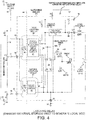
- FIG. 4 is a circuit diagram that shows how the capacitor 21 is used to supply a local supply node 63.
- the capacitor 21 is coupled to and supplies the local supply node 63 via the storage terminal 39.
- the local supply node 63 supplies circuitry of the latching relay 11.
- the local supply node 63 is coupled to the first coupling circuit 22, to a cathode of the diode 26, to the voltage regulator 25, to a source terminal of the pMOS transistor 32, and to the latch circuit 24.
- the capacitor 21 is external to the latching relay 11.
- the capacitor 21 has one terminal coupled to the storage terminal 39 and another terminal coupled to ground 20.
- the conductor 21 is internal and within the latching circuit 11 and no storage terminal is provided with the latching circuit 11.
- FIG. 5 is a circuit diagram showing how the latching relay is used to enable the load 13.
- the microcontroller 12 controls the set/refresh control signal 49 to switch from a digital logic high level to a digital logic low level.
- the first coupling circuit 22 sinks current from the supply node 14.
- Reference numeral 64 represents this flow of current.
- Current flow through LED 40 causes photodiode 52 to be activated and pulls node 72 low. This in turn sets an S input of latch circuit 24.
- latch circuit 24 outputs a digital logic high signal 66 on a Q output terminal of the latch circuit 24.
- Inverter 29 receives and inverts the digital logic high signal 66 and supplies a digital logic low signal 67 onto a gate of the PMOS transistor 32 thereby enabling the PMOS transistor 32.
- the local supply node 63 biases a gate of drive transistor 30 thereby enabling drive transistor 30.
- the load 13 is switched on and drive current 65 flows from the load supply 15, through load 13, through load terminal 37, through drive transistor 30, and onto a negative terminal of load supply 15 via terminal 38.
- the set/refresh control signal 49 is switched to a digital logic high level and current stops flowing through LED 40 of the first coupling circuit 22.
- the capacitor 21 begins to discharge. As the capacitor 21 discharges, the local supply node 63 decreases in voltage. Discharge of capacitor 21 is undesirable because the drive transistor 30 is maintained in a conductive state by supplying the gate of the drive transistor 30 from the local supply node 63. If the capacitor 21 were to discharge to such an extent that the drive transistor 30 were to switch off and no longer be conductive, then the load current 65 would stop flowing and the load 13 would switch off. As explained below with respect to FIG. 6 , the latching relay 11 is controlled in a refresh mode thereby re-charging capacitor 21 from the supply terminal 33 and not from the load terminal 37.
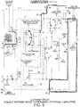
- FIG. 6 is a circuit diagram showing how the capacitor 21 is recharged by controlling the latching relay 11 in a refresh mode.
- microcontroller 12 controls the latching relay 11 to operate in a refresh mode.
- the set/refresh control signal 49 is pulsed with a duty cycle of a predetermined fractional amount.
- the duty cycle of the set/refresh control signal 49 in the refresh mode is pre-determined based on design factors including integrated circuit leakages, external MOSFET leakages, and board leakages.
- the capacitor 21 is charged from the supply node 14 via the supply terminal 33.
- the capacitor 21 is not charged from the load supply 15 or from the load terminal 37 in the refresh mode.
- the set/refresh control signal 49 is controlled to a digital logic high level in the refresh mode, no current flows through the LED 40 of coupling circuit 22. Neither the LED 40 nor the photovoltaic stack 51 is enabled. Accordingly, the capacitor is not charged when the set/refresh control signal 49 is controlled to a digital logic high level.
- the LED 40 sinks current from the supply node 14 via the supply terminal 33 onto the control terminal 34. This causes the LED 40 to be enabled and to radiate energy that is absorbed by the photovoltaic stack 51 thereby enabling the photovoltaic stack 51.
- a voltage +V develops across the photovoltaic stack 51.
- the voltage +V across the photovoltaic stack 51 charges the capacitor 21 via the diode 26 and storage terminal 39.
- Reference numeral 68 identifies a current path from the PVSPD circuit 41 that charges the capacitor 21. Accordingly, the capacitor 21 is charged during the low cycle of the set/refresh control signal 49.
- FIG. 7 is a circuit diagram showing how the latching relay switches the load 13 from an enabled state to a disabled state.
- the microcontroller 12 controls the reset control signal 50 to switch from a digital logic high level to a digital logic low level.
- the second coupling circuit 23 sinks current from the supply node 14.
- Reference numeral 69 represents this flow of current.
- Current flow through LED 42 causes photodiode 54 to be activated and pulls node 70 low. This in turn sets an R input of latch circuit 24.
- the latch circuit 24 outputs a digital logic low signal 66 on the Q output terminal and outputs a digital logic high signal 71 on the Q output terminal.
- Inverter 29 receives and inverts the digital logic low signal 66 and supplies a digital logic high signal 67 onto the gate of the PMOS transistor 32 thereby disabling the PMOS transistor 32.
- the digital logic high signal 71 is supplied onto a gate of the NMOS transistor 31 thereby enabling the NMOS transistor 31.
- the gate of the drive transistor 30 is pulled low via the NMOS transistor 31 thereby disabling drive transistor 30.
- the load 13 is switched off.
- the reset control signal 50 is switched to a digital logic high level and current stops flowing through LED 42 of the second coupling circuit 23.
- FIG. 8 is a waveform diagram of voltage and current along various nodes of system 10 during operation of latching relay 11.
- the latching relay is connected to the load 13 as shown in FIG. 3 .
- the capacitor 21 begins to charge up from trickle current 62.
- the voltage on the local supply node 63 begins increasing.
- the capacitor 21 is fully charged as shown in FIG. 4 .
- the local supply node 63 is at 12.0V. It is appreciated by one of ordinary skill in the art that the voltage of the local supply node 63 is configurable to other voltages depending on the operating characteristics of the capacitor 21 that is selected and upon the load requirements of load 13.
- the microcontroller 12 controls the latching relay 11 to enable the load 13 as shown in FIG. 5 .
- the set/refresh control signal 49 is switched from a digital logic high level to a digital logic low level which initiates turn on of the load 13.
- the load current 65 increases. In this example, the load current 65 reaches 5mA, but it is appreciated that the load current would reach different current levels depending on the load.
- the local supply node 63 decreases due to discharge of the capacitor 21.
- the local supply node 63 increases due to LED 40 being enabled which causes the local supply node 63 to be charged.
- the microcontroller 12 controls the latching relay 11 to operate in the refresh mode.
- the refresh mode extends from time T5 to time T11.
- the set/refresh control signal 49 is switched from a digital logic high level to a digital logic low level and capacitor 21 is charged thereby causing the voltage on the local supply node 63 to increase.
- the set/refresh control signal 49 is switched from a digital logic low level to a digital logic high level and capacitor 21 is discharged thereby causing the voltage on the local supply node 63 to decrease.
- This pulsing sequence is repeated as shown across times T8, T9, and T10.
- Reference numeral 73 identifies a relationship between the time the set/refresh control signal 49 is low (T P ) and the time the set/refresh control signal 49 is high (T REF ) in one example embodiment.
- Current I SC represents the current available to charge the capacitor from the photovoltaic stack 51 when the set/refresh control signal 49 is low.
- Current I DIS represents current consumed when the set/refresh control signal 49 is high and the capacitor 21 is discharging. Relationship 73 is required to prevent the voltage on the local supply node 63 from decreasing below the minimum operating voltage of the latching relay 11.
- the microcontroller 12 controls the latching relay 11 to disable the load 13.
- the reset control signal 50 is switched from a digital logic high level to a digital logic low level which initiates turn off of the load 13. From time T11 to time T12, the load current 65 decreases until it reaches zero. After time T11, the load 13 is disabled and off.
- FIG. 9 is a flowchart of a method 100 in accordance with one novel aspect.
- a load terminal of a latching relay is coupled to a load.
- the load charges a capacitor via the load terminal while the load remains in a disabled state.
- the latching relay 11 is connected to the load 13 via the load terminal 37.
- the load 13 is off and the siren is not ringing.
- the load 13 is supplied by the load supply 15.
- the latching relay 11 is coupled to the voltage supply 14 via supply node 33.
- the latching relay 11 is controlled by the microcontroller 12 via the control terminals 34 and 35.
- the capacitor 21 supplies the local supply node 63 via the storage terminal 39. As shown in FIG. 4 , the capacitor 21 begins to discharge as circuitry of the latching relay is supplied by the local supply node 63.
- a second step the load is switched from the disabled state to the enabled state such that current flows from the load supply, through the load, through the latching relay, and to another terminal of the latching relay.
- the capacitor supplies the latching relay while the load is in the enabled state.
- the microcontroller 12 controls the latching relay 11 to enable the load 13 by driving the set/refresh control signal 49 to a digital logic low level.
- the drive transistor 30 is enabled and the load 13 is switched on causing the siren to ring. Current flows from the load supply 15, through load 13, through load terminal 37, through a source of transistor 30, and to the negative terminal of the load supply 15 via the return terminal 38.
- a third step (step 103) the capacitor is charged by pulsing current through a supply terminal of the latching relay.
- the capacitor is charged while the load is in the enabled state.
- the microcontroller 12 controls the latching relay 11 to operate in the refresh mode by pulsing the set/refresh control signal 49.
- the set/refresh control signal 49 is pulsed in accordance with a pre-determined duty cycle. Pulsing the set/refresh control signal 49 causes current to sink through LED 40 and results in LED 40 radiating energy onto photovoltaic stack 51. A voltage V+ develops across the photovoltaic stack 51 that charges the capacitor 21 via diode 26 and storage terminal 39.
- a fourth step the load is switched from the enabled state to the disabled state.
- the microcontroller 12 controls the latching relay 11 to disable the load 13 by driving the reset signal 50 to a digital logic low level.
- the drive transistor 30 is disabled and the load 13 is switched off causing the siren to stop ringing.
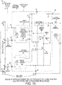
- FIG. 10 is a circuit diagram of another configuration of latching relay 11 where the load supply 15 is directly coupled to the load supply terminal 36 thereby avoiding the need for capacitor 21 or for refresh mode operation.
- the load supply is accessible, such as in the example of FIG. 10
- the load supply 15 is directly connected to the latching relay 11 and no capacitor, such as capacitor 21 of FIG. 1 , is needed.
- the latching relay 11 need not operate in the refresh mode when the latching relay 11 is latched on because the local supply node 63 is supplied from the load supply 15.
- voltage regulator 25 in turn supplies the local supply node 63. As long as there is sufficient energy stored in the load supply 15 to maintain the local supply node 63 above the minimum operating voltage level, then the latching relay 11 will remain enabled and the load 13 will remain on.
- FIG. 11 is a circuit diagram of another embodiment of a packaged latching relay 200 where drive transistor 201 is outside of the latching relay.
- the packaged latching relay 200 of FIG. 11 has substantially the same structure as the latching relay 11 of FIG. 1 except that the drive transistor 201 is outside of the packaged latching relay 200.
- packaged latching relay 200 includes a drive terminal 202 that drives a gate of the transistor 201.
- the packaged latching relay 200 of FIG. 11 operates in substantially the same way as the latching relay 11 of FIG. 1 , but the packaged latching relay 200 is smaller and cheaper to manufacture due to the one less transistor disposed within the package.
- the packaged latching relay 200 offers flexibility in that the packaged latching relay 200 is configurable to drive a wide variety of drive transistors.
Landscapes
- Electronic Switches (AREA)
- Relay Circuits (AREA)
Applications Claiming Priority (1)
| Application Number | Priority Date | Filing Date | Title |
|---|---|---|---|
| US16/104,920 US10523198B1 (en) | 2018-08-19 | 2018-08-19 | Optically isolated latching solid state relay with low on resistance and linear operation |
Publications (2)
| Publication Number | Publication Date |
|---|---|
| EP3624340A2 true EP3624340A2 (de) | 2020-03-18 |
| EP3624340A3 EP3624340A3 (de) | 2020-07-22 |
Family
ID=67659325
Family Applications (1)
| Application Number | Title | Priority Date | Filing Date |
|---|---|---|---|
| EP19192377.0A Withdrawn EP3624340A3 (de) | 2018-08-19 | 2019-08-19 | Optisch isoliertes verriegelungsfestkörperrelais mit geringem einschaltwiderstand und linearem betrieb |
Country Status (4)
| Country | Link |
|---|---|
| US (2) | US10523198B1 (de) |
| EP (1) | EP3624340A3 (de) |
| CN (1) | CN110838837B (de) |
| TW (2) | TWI866845B (de) |
Families Citing this family (1)
| Publication number | Priority date | Publication date | Assignee | Title |
|---|---|---|---|---|
| JP7374948B2 (ja) * | 2021-03-23 | 2023-11-07 | 株式会社東芝 | 半導体リレー装置 |
Citations (2)
| Publication number | Priority date | Publication date | Assignee | Title |
|---|---|---|---|---|
| US6339236B1 (en) * | 1999-09-27 | 2002-01-15 | Matsushita Electric Works, Ltd. | Light responsive semiconductor switch with shorted load protection |
| US20070201254A1 (en) * | 2006-02-28 | 2007-08-30 | Naoki Sakurai | Motor drive |
Family Cites Families (11)
| Publication number | Priority date | Publication date | Assignee | Title |
|---|---|---|---|---|
| US4147964A (en) * | 1978-02-09 | 1979-04-03 | Rca Corporation | Complementary latching disabling circuit |
| US4644288A (en) * | 1985-01-09 | 1987-02-17 | Crown International, Inc. | Method of fault sensing for power amplifiers having coupled power stages with normally alternate current flow |
| US4709160A (en) * | 1986-08-25 | 1987-11-24 | Rockwell International Corporation | Solid state dc power switch |
| FR2605161B1 (fr) * | 1986-10-08 | 1991-09-13 | Aerospatiale | Commutateur electronique a faible chute de tension |
| US5440440A (en) * | 1994-02-03 | 1995-08-08 | Teledyne Industries, Inc. | High current solid state AC relay with low EMI emission |
| US6603221B1 (en) * | 1999-04-22 | 2003-08-05 | Zhongdu Liu | Solid state electrical switch |
| JP3572292B2 (ja) * | 2002-01-29 | 2004-09-29 | 松下電器産業株式会社 | スイッチング電源回路 |
| US7196436B2 (en) * | 2003-04-03 | 2007-03-27 | Goodrich Corporation | Solid state relay for switching AC power to a reactive load and method of operating the same |
| TWI249287B (en) * | 2003-06-25 | 2006-02-11 | Matsushita Electric Works Ltd | Electronic switch |
| US20060245129A1 (en) | 2005-05-02 | 2006-11-02 | Bamburak Peter K | Latching solid state relay |
| US9374076B2 (en) * | 2012-03-06 | 2016-06-21 | Mcq Inc. | Solid state relay circuit |
-
2018
- 2018-08-19 US US16/104,920 patent/US10523198B1/en active Active
-
2019
- 2019-08-16 TW TW113115010A patent/TWI866845B/zh active
- 2019-08-16 TW TW108129181A patent/TWI842731B/zh active
- 2019-08-19 EP EP19192377.0A patent/EP3624340A3/de not_active Withdrawn
- 2019-08-19 CN CN201910766788.XA patent/CN110838837B/zh active Active
- 2019-12-06 US US16/706,531 patent/US10833675B2/en active Active
Patent Citations (2)
| Publication number | Priority date | Publication date | Assignee | Title |
|---|---|---|---|---|
| US6339236B1 (en) * | 1999-09-27 | 2002-01-15 | Matsushita Electric Works, Ltd. | Light responsive semiconductor switch with shorted load protection |
| US20070201254A1 (en) * | 2006-02-28 | 2007-08-30 | Naoki Sakurai | Motor drive |
Also Published As
| Publication number | Publication date |
|---|---|
| US10523198B1 (en) | 2019-12-31 |
| TWI842731B (zh) | 2024-05-21 |
| TWI866845B (zh) | 2024-12-11 |
| CN110838837A (zh) | 2020-02-25 |
| TW202433855A (zh) | 2024-08-16 |
| TW202027420A (zh) | 2020-07-16 |
| EP3624340A3 (de) | 2020-07-22 |
| US20200112309A1 (en) | 2020-04-09 |
| CN110838837B (zh) | 2025-02-21 |
| US10833675B2 (en) | 2020-11-10 |
Similar Documents
| Publication | Publication Date | Title |
|---|---|---|
| US11201619B2 (en) | Isolated high side drive circuit | |
| CN113098469A (zh) | 用于GaN开关的时间可编程失效安全下拉电路 | |
| CN1856928B (zh) | 功率控制系统启动和禁止方法 | |
| CN112119589B (zh) | 用于控制p沟道mosfet的驱动器电路和包括其的控制装置 | |
| US20210184585A1 (en) | Switching control circuit and power supply circuit | |
| US7554367B2 (en) | Driving circuit | |
| JP7314783B2 (ja) | スイッチング制御回路、電源回路 | |
| US20100097043A1 (en) | Inductor driving circuit | |
| US10833675B2 (en) | Optically isolated latching solid state relay with low on resistance and linear operation | |
| US12074589B2 (en) | Semiconductor device | |
| US7176657B2 (en) | Capacitor charging circuit with a soft-start function | |
| JP2014150654A (ja) | ゲート駆動回路 | |
| US12494781B2 (en) | Semiconductor relay device | |
| JP5226474B2 (ja) | 半導体出力回路 | |
| KR102213409B1 (ko) | 구동기 회로 및 그 동작 방법 | |
| JP2013033873A (ja) | 半導体装置 | |
| JP7055714B2 (ja) | 半導体装置 | |
| JP2025172516A (ja) | 保護装置 |
Legal Events
| Date | Code | Title | Description |
|---|---|---|---|
| PUAI | Public reference made under article 153(3) epc to a published international application that has entered the european phase |
Free format text: ORIGINAL CODE: 0009012 |
|
| STAA | Information on the status of an ep patent application or granted ep patent |
Free format text: STATUS: THE APPLICATION HAS BEEN PUBLISHED |
|
| AK | Designated contracting states |
Kind code of ref document: A2 Designated state(s): AL AT BE BG CH CY CZ DE DK EE ES FI FR GB GR HR HU IE IS IT LI LT LU LV MC MK MT NL NO PL PT RO RS SE SI SK SM TR |
|
| AX | Request for extension of the european patent |
Extension state: BA ME |
|
| PUAL | Search report despatched |
Free format text: ORIGINAL CODE: 0009013 |
|
| AK | Designated contracting states |
Kind code of ref document: A3 Designated state(s): AL AT BE BG CH CY CZ DE DK EE ES FI FR GB GR HR HU IE IS IT LI LT LU LV MC MK MT NL NO PL PT RO RS SE SI SK SM TR |
|
| AX | Request for extension of the european patent |
Extension state: BA ME |
|
| RIC1 | Information provided on ipc code assigned before grant |
Ipc: H03K 17/785 20060101AFI20200617BHEP |
|
| STAA | Information on the status of an ep patent application or granted ep patent |
Free format text: STATUS: REQUEST FOR EXAMINATION WAS MADE |
|
| 17P | Request for examination filed |
Effective date: 20210120 |
|
| RBV | Designated contracting states (corrected) |
Designated state(s): AL AT BE BG CH CY CZ DE DK EE ES FI FR GB GR HR HU IE IS IT LI LT LU LV MC MK MT NL NO PL PT RO RS SE SI SK SM TR |
|
| STAA | Information on the status of an ep patent application or granted ep patent |
Free format text: STATUS: EXAMINATION IS IN PROGRESS |
|
| 17Q | First examination report despatched |
Effective date: 20230707 |
|
| STAA | Information on the status of an ep patent application or granted ep patent |
Free format text: STATUS: THE APPLICATION IS DEEMED TO BE WITHDRAWN |
|
| 18D | Application deemed to be withdrawn |
Effective date: 20240118 |