EP3621202A1 - Adaptiver mehrstufiger gate-treiber - Google Patents
Adaptiver mehrstufiger gate-treiber Download PDFInfo
- Publication number
- EP3621202A1 EP3621202A1 EP19020501.3A EP19020501A EP3621202A1 EP 3621202 A1 EP3621202 A1 EP 3621202A1 EP 19020501 A EP19020501 A EP 19020501A EP 3621202 A1 EP3621202 A1 EP 3621202A1
- Authority
- EP
- European Patent Office
- Prior art keywords
- input
- coupled
- output
- gate
- current
- Prior art date
- Legal status (The legal status is an assumption and is not a legal conclusion. Google has not performed a legal analysis and makes no representation as to the accuracy of the status listed.)
- Granted
Links
Images






Classifications
-
- H—ELECTRICITY
- H03—ELECTRONIC CIRCUITRY
- H03K—PULSE TECHNIQUE
- H03K17/00—Electronic switching or gating, i.e. not by contact-making and –breaking
- H03K17/04—Modifications for accelerating switching
- H03K17/0406—Modifications for accelerating switching in composite switches
-
- H—ELECTRICITY
- H03—ELECTRONIC CIRCUITRY
- H03K—PULSE TECHNIQUE
- H03K17/00—Electronic switching or gating, i.e. not by contact-making and –breaking
- H03K17/04—Modifications for accelerating switching
- H03K17/041—Modifications for accelerating switching without feedback from the output circuit to the control circuit
- H03K17/0412—Modifications for accelerating switching without feedback from the output circuit to the control circuit by measures taken in the control circuit
-
- H—ELECTRICITY
- H02—GENERATION; CONVERSION OR DISTRIBUTION OF ELECTRIC POWER
- H02M—APPARATUS FOR CONVERSION BETWEEN AC AND AC, BETWEEN AC AND DC, OR BETWEEN DC AND DC, AND FOR USE WITH MAINS OR SIMILAR POWER SUPPLY SYSTEMS; CONVERSION OF DC OR AC INPUT POWER INTO SURGE OUTPUT POWER; CONTROL OR REGULATION THEREOF
- H02M1/00—Details of apparatus for conversion
- H02M1/08—Circuits specially adapted for the generation of control voltages for semiconductor devices incorporated in static converters
-
- H—ELECTRICITY
- H03—ELECTRONIC CIRCUITRY
- H03K—PULSE TECHNIQUE
- H03K17/00—Electronic switching or gating, i.e. not by contact-making and –breaking
- H03K17/16—Modifications for eliminating interference voltages or currents
- H03K17/161—Modifications for eliminating interference voltages or currents in field-effect transistor switches
- H03K17/162—Modifications for eliminating interference voltages or currents in field-effect transistor switches without feedback from the output circuit to the control circuit
- H03K17/163—Soft switching
-
- H—ELECTRICITY
- H03—ELECTRONIC CIRCUITRY
- H03K—PULSE TECHNIQUE
- H03K17/00—Electronic switching or gating, i.e. not by contact-making and –breaking
- H03K17/16—Modifications for eliminating interference voltages or currents
- H03K17/168—Modifications for eliminating interference voltages or currents in composite switches
-
- H—ELECTRICITY
- H03—ELECTRONIC CIRCUITRY
- H03K—PULSE TECHNIQUE
- H03K17/00—Electronic switching or gating, i.e. not by contact-making and –breaking
- H03K17/51—Electronic switching or gating, i.e. not by contact-making and –breaking characterised by the components used
- H03K17/56—Electronic switching or gating, i.e. not by contact-making and –breaking characterised by the components used by the use, as active elements, of semiconductor devices
- H03K17/567—Circuits characterised by the use of more than one type of semiconductor device, e.g. BIMOS, composite devices such as IGBT
-
- H—ELECTRICITY
- H03—ELECTRONIC CIRCUITRY
- H03K—PULSE TECHNIQUE
- H03K2217/00—Indexing scheme related to electronic switching or gating, i.e. not by contact-making or -breaking covered by H03K17/00
- H03K2217/0036—Means reducing energy consumption
-
- H—ELECTRICITY
- H03—ELECTRONIC CIRCUITRY
- H03K—PULSE TECHNIQUE
- H03K2217/00—Indexing scheme related to electronic switching or gating, i.e. not by contact-making or -breaking covered by H03K17/00
- H03K2217/0081—Power supply means, e.g. to the switch driver
Definitions
- the present invention relates generally to a system and method for an adaptive multilevel gate driver.
- FIG. 1A is a schematic 100 of an Integrated Gate Bipolar Transistor ("IGBT") 102 including parasitic capacitances C M coupled between the gate and the collector, C GE coupled between the gate and the emitter, and C CE coupled between the collector and the emitter.
- IGBT Integrated Gate Bipolar Transistor
- Figure 1B is a graph of values of the parasitic capacitances shown in Fig. 1A with respect to collector-emitter voltage, wherein C ISS represents the sum of the C M and C GE capacitors, Coss represents the sum of the C M and C CE capacitors, and C M represents the Miller capacitor, which is highly non-linear due the gain of IGBT 102, as is known in the art.
- the values of capacitors C ISS , C OSS , and C M are relatively high for a low collector-emitter voltage, and rapidly decrease during an initial increase in the collector-emitter voltage, and then asymptotically approach a minimum value at high collector-emitter voltages.
- FIG. 2A is a schematic diagram 200 of a prior art power switch including a high side driver 206 and a low side driver 204, a high side gate resistor RgHS and a low side gate resistor RgLS, as well as a high side power transistor T1 and a low side power transistor T2.
- Voltages V CE collector-to-emitter voltage
- V G gate voltage
- V OUT voltage from the low side gate driver
- currents I G (gate current) and Ic collector current
- the propagation delay of the power transistors shown in Fig. 2A is also relatively high. Portions of the propagation delay of the power transistors is referred to as "dead time" that must be considered in half-bridge applications in order to avoid cross-conduction. Large propagation delays for both the high side device and the low side device of a half-bridge power switch exist dominantly at turn-off when the collector-to-emitter voltage ("VCE") or the drain-to-source voltage (“VDS”) is low. As depicted in Fig.iB, in this case the Miller capacitance is very high. The long propagation delay causes a large dead time as the propagation delay at turn-on is short. This causes disadvantages in efficiency and precise timing.
- VCE collector-to-emitter voltage
- VDS drain-to-source voltage
- One solution for addressing propagation delays is by a suitable selection of the gate resistors RgLS and RgHS.
- the gate resistance also specifies switching speed.
- the selection of the gate resistor Rg is limited by other design constraints, such as dv/dt restrictions of Electro-Magnetic Interference ("EMI") limitations.
- EMI Electro-Magnetic Interference
- Figure 2B is a timing diagram associated with the power switch of Fig. 2A showing the V OUT , V G , I G , V CE , and Ic waveforms for a given value of RgHS and RgLS. Also shown in Fig. 2B is the I OFF waveform, which is the turn off current.
- Figure 3A is a more detailed timing diagram associated with a turn-on phase of the low side of the power switch of Fig. 2A
- Figure 3B is a more detailed timing diagram associated with a turn-off phase of the low side of the power switch of Fig. 2A
- the waveforms shown in Figs. 3A and 3B include the gate voltage (V G ), output voltage (V S ), gate current (I G ), collector current (I C ), and energy losses (E).
- the time parameters along the horizontal time axis of these waveforms include: t TH (time when the threshold voltage is achieved), t 1 (time when the Miller plateau starts), t2 (time when the tail begins in the turn-on mode or ends in the turn-off mode), and t 3 (time when the Miller plateau finishes).
- dead time and the tail phenomenon are both minimized, which in turn improves switching efficiency and allows for more precise switch timing of a power switch.
- a gate driver circuit for driving a power switch comprises a gate driver having a first input for receiving an input signal and an output coupled to the power switch, the gate driver configured for providing a primary gate current and an auxiliary gate current; and a differential voltage sensor having a first input for receiving the input signal, a second input coupled to a power supply voltage, a third input coupled to a terminal of the power switch, and an output coupled to a second input of the gate driver.
- the gate current of the output stage of the gate driver for a power switch is configured, to depend upon the difference between the output voltage Vs of the switch and the supply voltages of the switch (Vss and DC+).
- Vss is a negative voltage supply or ground
- DC+ is a positive voltage supply.
- the absolute value of these voltages can range from the tens of volts to hundreds of volts as required for a specific application and as allowed by a specific switch technology.
- Figure 4A is a timing diagram associated with a turn-on phase of the low side of a power switch according to an embodiment
- Figure 4B is a timing diagram associated with a turn-off phase of the low side of the power switch according to an embodiment.
- the following waveforms are shown in Figs. 4A and 4B : gate voltage (V G ); output voltage (V S ); gate current (I G ); collector current (I C ); energy losses (E).
- the energy losses are shown having an Esw and an E COND portion as previously described.
- Portion 402 of the V S waveform (between times t 2 and t 3 ) indicate an erased tail during turn-on.
- Portion 404 of the I G waveform (between times t 2 and t 4 ) shows a boost gate current.
- Portion 406 of the V S waveform (between times t 1 and t 2 ) indicate an erased tail during turn-off.
- Portion 408 of the I G waveform (between times t 0 and t 2 ) again shows the boost gate current.
- the tails in portions 402 and 406 of the V S waveforms can be erased. This enables minimizing switching losses and the dead time, while also keeping the dv/dt of the switching devices within the limits imposed by EMI regulations.
- the correct level of gate boost current is provided at the gate of the high side and low side power devices, during both turn-on and turn-off phases.
- the exact mechanism for creating the differential voltages ⁇ V LS and ⁇ V HS is explained in further detail below, particularly with the description of input stages that are shown in Figs. 14 and 15 .
- ⁇ V th an average value (threshold) of ⁇ V was found at which Vs starts showing the previously described tail phenomenon (see arrow portions in Figs. 3A and 3B ).
- This threshold value of ⁇ V is hereinafter referred to as ⁇ V th .
- the initial portion of the tail phenomenon corresponds to the peak value of the Miller capacitance. Once ⁇ V reaches or falls below ⁇ V th , the gate current is boosted.
- FIG. 5A is a block diagram of an integrated circuit gate driver 501 and a half bridge power switch 503 of a power switching system 500A according to an embodiment.
- the power switching system is substantially symmetrical as it is comprised of similar blocks both at low and at high side.
- the integrated circuit gate driver 501 is described below.
- the half bridge power switch 503 includes high side power device 526 such as an IGBT coupled between DC+ and the output voltage node V S , which in turn is coupled to a load 530. While an inductive load is shown, other types of loads are known in the art.
- a freewheeling diode D3 is coupled across the current path of power device 526, in an embodiment.
- the half bridge power switch 503 also includes low side power device 528 such as an IGBT coupled between the output voltage node V S , and the V SS power supply node, which is shown as ground in an embodiment.
- low side power device 528 such as an IGBT coupled between the output voltage node V S , and the V SS power supply node, which is shown as ground in an embodiment.
- a freewheeling diode D4 is coupled across the current path of power device 528, in an embodiment.
- An embodiment integrated circuit gate driver 501 is shown in Fig. 5A , including the following pins (in clockwise order): DC+ (positive power supply voltage), V B (internal biasing node), H 01 (first high side gate driver output), H 02 (second high side gate driver output), V S (output voltage node), L 02 (second low side gate driver output), L 01 (first low side gate driver output), V SS (ground or negative supply voltage), L IN (low side input signal), H IN (high side input signal), V CC (additional positive power supply voltage).
- DT dead time circuit used to insert a time interval between the high side and low side switching signals in order avoid simultaneous switching of the power devices
- AST Anti-Shot-Through circuit used in
- HZ is also used in Fig. 5A , referring to high side boost current driver 520 and low side boost current driver 522.
- the abbreviation “HZ” refers to a high impedance output state in which drivers 520 and 522 can be placed when not supplying the boosted gate current pulses as is described in further detail below.
- the auxiliary stages 520 and 522 are set in order to show a high impedance (HZ) whenever the auxiliary boost current is not needed.
- Gate driver circuit 501 can be configured to omit some of the above described functional blocks for a specific application, or to add additional functional blocks for a specific application as desired.
- lower voltages blocks 502, 504, 506, 508, 516, 522, 524, and D2 can all be integrated on a P-substrate portion of the gate driver integrated circuit 501.
- high voltage blocks 510, 512, 514, 518, 520, and D1 can all be integrated on an N-epitaxial portion of the gate driver integrated circuit 501.
- Figure 5B is a block diagram of a power switching system 500B including a gate driver 522, 524, a low side differential voltage sensor 516, diodes D2 and D4, and a single transistor power switch 528 having an emitter referenced to V SS and a collector coupled to load 530.
- Figure 5C is a block diagram of a power switching system 500C including a gate driver 518, 520, a hide side differential voltage sensor 514, diodes D1 and D3, and a single transistor power switch having an collector referenced to DC+ and an emitter coupled to load 530.
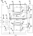
- Figure 6 is a block diagram of the low side differential voltage sensor 516 associated with the power switching system 500A of Fig. 5A .
- Low side sensor and differentiator circuit 516 is shown in greater detail in block diagram form in Fig. 6 .
- Low side sensor circuit 516 includes a diode D2 previously described, and an input stage 604 for providing three references voltages including the VS_DIODE reference voltage, the VREF reference voltage, and the REF reference voltage.
- the input stage is shown in further detail in Fig. 14 , and described in further detail below.
- Low side sensor and differentiator circuit 516 also includes a differentiator 608 including capacitor 602 and resistor 606, a comparator 610, and a logic circuit 612.
- the differentiator 608 receives the V REF reference signal and is associated with the input IN DER and output OUT DER signals.
- the comparator 610 receives the REF reference signal and provides the LS VCESENSE output signal.
- the logic circuit 612 receives the LS VCE-SENSE and L IN signals and provides the LS Pull-up Boost and LS Pull-down Boost signals.
- the differentiator 608 and comparator 610 may be of conventional design.
- Logic circuit 612 can be implemented using logic gates in an integrated circuit or as software internal or external to the integrated circuit as desired. The exact logic function for logic circuit 612 can be discerned from the various timing diagrams that are provided and described in further detail below.
- diode D2 In operation, once the sensed ⁇ V LS crosses a pre-established threshold as discussed above, diode D2 provides a signal that follows the shape of the ⁇ V LS . This signal is subsequently provided to the input of the differentiator 608 together with an adaptive voltage reference (V REF ). At the input of the differentiator (IN DER ) there are pulses centered around the V REF voltage level, which are coherent with the slope of the signal provided by the input stage 604.
- V REF adaptive voltage reference
- a pulse over the V REF level occurs whenever ⁇ V LS decreases and a pulse under the V REF level occurs in the opposite case.
- This signal is input into comparator 610 which, in conjunction with reference voltage (REF), provides the LS VCESENSE signal.
- a signal is required to provide an auxiliary current at the output of the power stage to provide a higher gate current when needed.
- the V REF signal of the differentiator 608 is managed to allow the first pulse of the differentiator 608 to last as long as the power transistor is switched on. This is done because on the rising edge of this output pulse a negative auxiliary gate current is provided to the power transistor, while on the falling edge a positive one is obtained, according to the polarity of the conventional constant gate current as presently used.
- the power stage 522 provides current pulses that will be added, at the output, to the constant gate current provided from the driver stage 524 marked "Constant current" in Fig. 5A in order to reduce the duration of the tail of VS and thus improving the power efficiency of the switching system.
- Figure 7 is a timing diagram associated with the low side differential voltage sensor 516 of Fig. 6 during a turn-on event including the Vs output signal including an erased tail portion according to an embodiment, the V S_DIODE signal, the V REF signal, the IN DER signal, the OUT DER signal, the REF reference voltage, the LS VCESENSE signal and the L IN input signal.
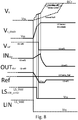
- Figure 8 is a timing diagram associated with the low side differential voltage sensor 516 of Fig. 6 during a turn-off event including the Vs output signal including an erased tail portion according to an embodiment, the V S_DIODE signal, the V REF signal, the IN DER signal, the OUT DER signal, the REF reference voltage, the LS VCESENSE signal and the L IN input signal.
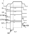
- Figure 9 is a timing diagram associated with the low side differential voltage sensor 516 of Fig. 6 during the turn-on and turn-off events including the V G gate voltage signal, the LS VCE-SENSE signal, the L IN input signal, the LS Pull-up Boost signal, the LS Pull-down Boost signal, the OUT DRIVER signal (output of boost driver 522), and the I G gate current signal.
- boost gate current portions can be clearly seen in FIG. 9 including boost current portion 902 during the second portion of a turn-on event and boost current portion 904 during the first portion of a turn-off event.
- the un-boosted gate current portions are provided by the low side constant current driver 524.
- Figure 10 is a block diagram of the high side differential voltage sensor 514 associated with the power switching system 500A of Fig. 5A .
- High side sensor and differentiator circuit 516 is shown in greater detail in block diagram form in Fig. 10 .
- High side sensor circuit 514 includes a diode D1 previously described, and an input stage 1004 for providing three references voltages including the DC _DIODE reference voltage, the VREF reference voltage, and the REF reference voltage.
- the input stage is shown in further detail in Fig. 15 , and described in further detail below.
- High side sensor circuit 514 also includes a differentiator 1008 including capacitor 1002 and resistor 1006, a comparator 1010, and a logic circuit 1012.
- the differentiator 1008 receives the V REF reference signal and is associated with the input IN DER and output OUT DER signals.
- the comparator 1010 receives the REF reference signal and provides the HS VCESENSE output signal.
- the logic circuit 1012 receives the HS VCESENSE and H IN signals and provides the HS Pull-up Boost and HS Pull-down Boost signals.
- the differentiator 1008 and comparator 1010 may be of conventional design.
- Logic circuit 1012 can be implemented using logic gates in an integrated circuit or as software internal or external to the integrated circuit as desired. The exact logic function for logic circuit 1012 can be discerned from the various timing diagrams that are provided and described in further detail below.
- diode D1 In operation, once the sensed ⁇ V HS crosses a pre-established threshold as discussed above, diode D1 provides a signal that follows the shape of the ⁇ V HS . This signal is subsequently provided to the input of the differentiator 1008 together with an adaptive voltage reference (V REF ). At the input of the differentiator (IN DER ) there are pulses centered around the V REF voltage level, which are coherent with the slope of the signal provided by the input stage 1004.
- V REF adaptive voltage reference
- a pulse over the VREF level occurs whenever ⁇ V HS decreases and a pulse under the V REF level occurs in the opposite case.
- This signal is input into comparator 1010 which, in conjunction with reference voltage (REF), provides the HS VCESENSE signal.
- a signal is required to provide an auxiliary current at the output of the power stage to provide a higher gate current when needed.
- the V REF signal of the differentiator 1008 is managed to allow the first pulse of the differentiator 1008 to last as long as the power transistor is switched on. This is done because on the rising edge of this output pulse a negative auxiliary gate current is provided to the power transistor, while on the falling edge a positive one is obtained, according to the polarity of the conventional constant gate current as presently used.
- the power stage 520 provides current pulses that will be added, at the output, to the constant gate current provided from the driver stage 518 marked "Constant current" in Fig. 5A in order to reduce the duration of the tail of V S and thus improving the power efficiency of the switching system.
- Figure 11 is a timing diagram associated with the high side differential voltage sensor 514 of Fig. 10 during a turn-on event including the Vsoutput signal including an erased tail portion according to an embodiment, the DC _DIODE signal, the V REF signal, the IN DER signal, the OUT DER signal, the REF reference voltage, the HS VCESENSE signal and the H IN input signal.
- Figure 12 is a timing diagram associated with the high side differential voltage sensor 514 of Fig. 10 during a turn-off event including the Vs output signal including an erased tail portion according to an embodiment, the DC _DIODE signal, the V REF signal, the IN DER signal, the OUT- DER signal, the REF reference voltage, the HS VCESENSE signal and the H IN input signal.
- Figure 13 is a timing diagram associated with the high side differential voltage sensor 514 of Fig. 10 during the turn-on and turn-off events including the V G gate voltage signal, the HS VCESENSE signal, the H IN input signal, the HS Pull-up Boost signal, the HS Pull-down Boost signal, the OUT DRIVER signal (output of boost driver 520), and the I G gate current signal.
- boost gate current portions can be clearly seen in FIG. 13 including boost current portion 1302 during the second portion of a turn-on event and boost current portion 1304 during the first portion of a turn-off event.
- the un-boosted gate current portions are provided by the low side constant current driver 518.
- Figure 14 is an exemplary schematic diagram of the low side input stage 604 suitable for use in the low side differential voltage sensor 516 of Fig. 6 .
- Transistor 1402 and six serially coupled diodes 1404 are used to create a reference voltage that is divided by resistors 1406 and 1408 to create the REF reference voltage.
- Transistor 1410 and six serially coupled diodes 1412 are used to create a reference voltage that is divided by resistors 1414, 1416, and 1418 to create the V REF reference voltage.
- Switch 1420 can be used to create two values for the V REF reference voltage.
- Transistor 1422 and four serially coupled diodes 1424, as well as Zener diode 1426 are used to create the V S_DIODE maximum allowed voltage, in conjunction with diode D2 as is explained in further detail below. It is important to note that the low side input stage 604 includes a connection to both V S (through diode D2) and directly to the V SS power supply voltage.
- the REF reference voltage is a substantially constant reference voltage above the V SS power supply level.
- the V REF reference voltage is a substantially constant reference voltage having a first nominal value above the V SS power supply level in a first mode of operation, and a second nominal value above the V SS power supply level in a second mode of operation.
- Switch 1420 is used to switch between the first and second modes of operation when V S_DIODE is over a transistor threshold voltage with respect to V SS turning the switch 1420 on, or when V S_DIODE goes under a transistor threshold voltage with respect to V SS , turning the switch 1420 off.
- the V S_DIODE voltage is a representative of the difference between the V S and V SS voltages as previously described.
- V S_DIODE When V S is more positive then the V S_DIODE maximum allowed voltage, the V S_DI-ODE voltage is clamped to a nominal value above V SS . However, when the V S voltage is more negative than the V S_DIODE maximum allowed voltage, the V S_DIODE voltage follows the V S voltage as can be seen in previous timing diagrams. The V S_DIODE is thus a representative voltage of the voltage across the low side power device 528.
- Figure 15 is an exemplary schematic diagram of the high side input stage 1004 suitable for use in the low side differential voltage sensor 516 of Fig. 6 .
- Transistor 1502 and six serially coupled diodes 1504 are used to create a reference voltage that is divided by resistors 1506 and 1508 to create the REF reference voltage.
- Transistor 1510 and six serially coupled diodes 1512 are used to create a reference voltage that is divided by resistors 1514, 1516, and 1518 to create the V REF reference voltage.
- Switch 1520 can be used to create two values for the V REF reference voltage.
- Transistor 1522 and four serially coupled diodes 1524, as well as Zener diode 1526 are used to create the DC _DIODE maximum allowed voltage, in conjunction with diode D1 as is explained in further detail below. It is important to note that the low side input stage 1004 includes a connection to both DC+ (through diode Di) and directly to the V S output voltage.
- the operation of the high side input stage 1004 of Fig. 15 is substantially the same as previously described with respect to the low side input stage 604 shown in Fig. 14 , except for the value of the various biasing, power supply, and reference voltages.
- the invention may further be illustrated by the following exemplary embodiments.
- a gate driver circuit for driving a power switch may comprise a gate driver having a first input for receiving an input signal and an output coupled to the power switch, the gate driver configured for providing a primary gate current and an auxiliary gate current and a differential voltage sensor having a first input for receiving the input signal, a second input coupled to a power supply voltage, a third input coupled to a terminal of the power switch, and an output coupled to a second input of the gate driver.
- the gate driver circuit may further comprise a primary driver configured for providing the primary gate current and an auxiliary driver configured for providing the auxiliary gate current.
- the primary driver may be coupled to the first input of the gate driver and the auxiliary driver is coupled to the second input of the gate driver.
- the differential voltage sensor of the gate driver circuit may comprise a differentiator having an input coupled to an input of the differential voltage sensor, and an input coupled to a differentiator reference voltage, a comparator having an input coupled to the output of the differentiator, an input coupled to a comparator reference voltage, and an output and a logic circuit having a first input coupled to the output of the comparator, a second input for receiving the input signal, and an output coupled to the output of the differential voltage sensor.
- the differential voltage sensor of the gate driver circuit may further comprise an input stage for generating the reference voltages for the differentiator and the comparator.
- the gate driver may further comprise a diode coupled between the second input of the differential voltage sensor and the power supply voltage.
- the gate driver may further comprise a diode coupled between the third input of the differential voltage sensor and the terminal of the power switch.
- a gate driver circuit for driving a power switch may comprise a first primary driver having an input for receiving a first input signal and an output for providing a first gate current, a first auxiliary driver having an input and an output for providing a first auxiliary gate current, a first differential voltage sensor having a first input for receiving the first input signal, a second input coupled to a first power supply voltage, a third input coupled to a terminal of the power switch, and an output coupled to the input of the first auxiliary driver, a second primary driver having an input for receiving a second input signal and an output for providing a second gate current, a second auxiliary driver having an input and an output for providing a second auxiliary gate current, and a second differential voltage sensor having a first input for receiving the second input signal, a second input coupled to a second power supply voltage, a third input coupled to the terminal of the power switch, and an output coupled to the input of the second auxiliary driver.
- the first differential voltage sensor of the gate driver circuit may comprise a differentiator having an input coupled to an input of the first differential voltage sensor, and an input coupled to a differentiator reference voltage, a comparator having an input coupled to an output of the differentiator and an input coupled to a comparator reference voltage, and a logic circuit having a first input coupled to an output of the comparator, a second input for receiving the first input signal, and an output coupled to the output of the first differential voltage sensor.
- the first differential voltage sensor of the gate driver circuit may further comprise an input stage for generating the reference voltages for the differentiator and the comparator.
- the logic circuit of the first differential voltage may comprise first and second outputs for driving first and second inputs of the first auxiliary driver.
- the second differential voltage sensor of the gate driver circuit may comprise a differentiator having an input coupled to an input of the second differential voltage sensor, and an input coupled to a differentiator reference voltage, a comparator having an input coupled to an output of the differentiator and an input coupled to a comparator reference voltage, and a logic circuit having a first input coupled to an output of the comparator, a second input for receiving the second input signal, and an output coupled to the output of the second differential voltage sensor.
- the second differential voltage sensor of the gate driver circuit may further comprise an input stage for generating the reference voltages for the differentiator and the comparator.
- the logic circuit of the second differential voltage may comprise first and second outputs for driving first and second inputs of the second auxiliary driver.
- a method for switching a half-bridge circuit including a high side device and a low side device may comprise driving a control node of the high side device with a first current pulse having a first pulse width, driving the control node of the high side device with a second current pulse during a duration of the first current pulse, having a second pulse width shorter than the first pulse width, driving a control node of the low side device with a third current pulse having a third pulse width, and driving the control node of the low side device with a fourth current pulse during a duration of the third current pulse, having a fourth pulse width shorter than the third pulse width.
- the first current pulse of the method may occur during first and second portions of a turn-on event of the high side device, and the second current pulse may occur only during the second portion of the turn-on event.
- the first current pulse of the method may occur during first and second portions of a turn-off event of the high side device, and the second current pulse may occur only during the first portion of the turn-off event.
- the third current pulse of the method may occur during first and second portions of a turn-on event of the low side device, and the fourth current pulse may occur only during the second portion of the turn-on event.
- the third current pulse of the method may occur during first and second portions of a turn-off event of the low side device, and the fourth current pulse may occur only during the first portion of the turn-off event.
- the second pulse width of the method may be determined by sensing and differentiating a voltage across the high side device, and wherein the fourth pulse width may be determined by sensing and differentiating a voltage across the low side device
Landscapes
- Engineering & Computer Science (AREA)
- Power Engineering (AREA)
- Electronic Switches (AREA)
- Power Conversion In General (AREA)
Applications Claiming Priority (1)
| Application Number | Priority Date | Filing Date | Title |
|---|---|---|---|
| US16/124,844 US10461730B1 (en) | 2018-09-07 | 2018-09-07 | Adaptive multi-level gate driver |
Publications (2)
| Publication Number | Publication Date |
|---|---|
| EP3621202A1 true EP3621202A1 (de) | 2020-03-11 |
| EP3621202B1 EP3621202B1 (de) | 2021-11-03 |
Family
ID=67847574
Family Applications (1)
| Application Number | Title | Priority Date | Filing Date |
|---|---|---|---|
| EP19020501.3A Active EP3621202B1 (de) | 2018-09-07 | 2019-09-02 | Adaptiver mehrstufiger gate-treiber |
Country Status (3)
| Country | Link |
|---|---|
| US (1) | US10461730B1 (de) |
| EP (1) | EP3621202B1 (de) |
| CN (1) | CN110890878B (de) |
Families Citing this family (15)
| Publication number | Priority date | Publication date | Assignee | Title |
|---|---|---|---|---|
| US10819237B1 (en) * | 2019-05-06 | 2020-10-27 | Texas Instruments Incorporated | Gate voltage plateau completion circuit for DC/DC switching converters |
| CN114616750B (zh) * | 2019-10-31 | 2026-01-23 | 株式会社田村制作所 | 栅极驱动电路 |
| JP7161509B2 (ja) * | 2019-10-31 | 2022-10-26 | 株式会社タムラ製作所 | ゲート駆動回路 |
| JP7401353B2 (ja) * | 2020-03-10 | 2023-12-19 | ローム株式会社 | 半導体装置 |
| US11431166B2 (en) * | 2020-04-02 | 2022-08-30 | Infineon Technologies Austria Ag | Electrostatic discharge protection in a monolithic gate driver having multiple voltage domains |
| US11362646B1 (en) | 2020-12-04 | 2022-06-14 | Skyworks Solutions, Inc. | Variable current drive for isolated gate drivers |
| US12155332B2 (en) | 2020-12-06 | 2024-11-26 | Skyworks Solutions, Inc. | Updating control parameters of a gate driver during operation |
| US11264985B1 (en) * | 2021-03-04 | 2022-03-01 | Aes Global Holdings Pte Ltd. | Bipolar pulsed-voltage gate driver |
| US11641197B2 (en) | 2021-04-28 | 2023-05-02 | Skyworks Solutions, Inc. | Gate driver output protection circuit |
| CN115514354A (zh) * | 2021-06-07 | 2022-12-23 | 英飞凌科技股份有限公司 | 栅极驱动器系统和在切换状态之间驱动晶体管的方法 |
| CN113472184B (zh) * | 2021-06-10 | 2023-12-15 | 矽力杰半导体技术(杭州)有限公司 | 驱动方法以及驱动电路 |
| JP7527251B2 (ja) * | 2021-07-27 | 2024-08-02 | 三菱電機株式会社 | 駆動回路及び半導体装置 |
| US11595035B1 (en) * | 2021-08-27 | 2023-02-28 | Infineon Technologies Ag | Method for reducing oscillation during turn on of a power transistor by regulating the gate switching speed control of its complementary power transistor |
| US12368374B2 (en) | 2023-07-20 | 2025-07-22 | Infineon Technologies Austria Ag | Protecting a power inverter by sensing a phase node voltage |
| US12388440B2 (en) * | 2023-12-28 | 2025-08-12 | Infineon Technologies Austria Ag | Gate driver |
Citations (1)
| Publication number | Priority date | Publication date | Assignee | Title |
|---|---|---|---|---|
| US5796276A (en) * | 1994-12-30 | 1998-08-18 | Sgs-Thomson Microelectronics, Inc. | High-side-driver gate drive circuit |
Family Cites Families (9)
| Publication number | Priority date | Publication date | Assignee | Title |
|---|---|---|---|---|
| US4043302A (en) * | 1975-08-25 | 1977-08-23 | Motorola, Inc. | Solid state ignition system and method for linearly regulating the dwell time thereof |
| US5687065A (en) * | 1994-11-28 | 1997-11-11 | Philips Electronics North America Corporation | Pre-regulator with light switch to limit voltage ringing on turn-off |
| JP4531075B2 (ja) * | 2007-05-16 | 2010-08-25 | 株式会社日立製作所 | 半導体回路 |
| US9203301B2 (en) * | 2010-06-23 | 2015-12-01 | Volterra Semiconductor Corporation | Feedback for controlling the switching frequency of a voltage regulator |
| JP6469118B2 (ja) * | 2014-01-28 | 2019-02-13 | シュナイダー エレクトリック アイティー コーポレーション | バイポーラゲートドライバ |
| CN103929162B (zh) * | 2014-04-30 | 2017-09-26 | 杭州士兰微电子股份有限公司 | 栅极驱动电路、功率开关电路以及栅极驱动方法 |
| US9571093B2 (en) * | 2014-09-16 | 2017-02-14 | Navitas Semiconductor, Inc. | Half bridge driver circuits |
| WO2017139406A1 (en) * | 2016-02-08 | 2017-08-17 | Witricity Corporation | Pwm capacitor control |
| KR102578357B1 (ko) * | 2016-12-16 | 2023-09-15 | 현대자동차주식회사 | 회로 소자 보호 회로, 상기 회로 소자 보호 회로가 설치된 차량, 회로 소자 보호 방법 및 차량의 제어 방법 |
-
2018
- 2018-09-07 US US16/124,844 patent/US10461730B1/en active Active
-
2019
- 2019-08-26 CN CN201910789988.7A patent/CN110890878B/zh active Active
- 2019-09-02 EP EP19020501.3A patent/EP3621202B1/de active Active
Patent Citations (1)
| Publication number | Priority date | Publication date | Assignee | Title |
|---|---|---|---|---|
| US5796276A (en) * | 1994-12-30 | 1998-08-18 | Sgs-Thomson Microelectronics, Inc. | High-side-driver gate drive circuit |
Also Published As
| Publication number | Publication date |
|---|---|
| CN110890878B (zh) | 2025-03-21 |
| EP3621202B1 (de) | 2021-11-03 |
| CN110890878A (zh) | 2020-03-17 |
| US10461730B1 (en) | 2019-10-29 |
Similar Documents
| Publication | Publication Date | Title |
|---|---|---|
| EP3621202B1 (de) | Adaptiver mehrstufiger gate-treiber | |
| US6501321B2 (en) | Level shift circuit | |
| US6333665B1 (en) | Gate circuit for insulated gate semiconductor device | |
| US11245324B2 (en) | Switching converter and a method thereof | |
| EP2164155B1 (de) | Ansteuerschaltung für elektronische elemente | |
| CN113098469A (zh) | 用于GaN开关的时间可编程失效安全下拉电路 | |
| AU726077B2 (en) | Gate control circuit for voltage drive switching element | |
| US20100283515A1 (en) | Gate driver for enhancement-mode and depletion-mode wide bandgap semiconductor jfets | |
| CN111492582B (zh) | 栅极驱动电路 | |
| US11451130B2 (en) | Circuit to transfer a signal between different voltage domains and corresponding method to transfer a signal | |
| US11881759B2 (en) | Circuit to transfer a signal between different voltage domains and corresponding method to transfer a signal | |
| US20170288661A1 (en) | Gate Driver That Drives With A Sequence Of Gate Resistances | |
| JP3937354B2 (ja) | ダイナミック・バックゲート・バイアスと短絡保護を伴うブートストラップ・ダイオード・エミュレータ | |
| JP3900178B2 (ja) | レベルシフト回路 | |
| US6813169B2 (en) | Inverter device capable of reducing through current | |
| JP4727360B2 (ja) | 絶縁ゲート型半導体素子のゲート回路 | |
| EP0177148A2 (de) | Leistungsversorgung mit MOSFET-Elementen | |
| JPH11234103A (ja) | パワートランジスタにおけるスイッチング動作の制御方法および装置 | |
| JP2024546764A (ja) | モータドライバにおける誘導接地バウンス電圧の低減のためのシステム及び方法 | |
| CN116633341A (zh) | 驱动装置的电位转换电路 | |
| US12407345B2 (en) | Switched inductive storage element to enhance gate drive at turn-off | |
| CN116961632A (zh) | 一种碳化硅mosfet多电平驱动电路及其控制方法 | |
| CN119865062A (zh) | 电压调节器电路、相应的驱动器电路、装置和操作方法 | |
| JPH09232929A (ja) | レベルシフト回路 | |
| JPH02134920A (ja) | 集積回路 |
Legal Events
| Date | Code | Title | Description |
|---|---|---|---|
| PUAI | Public reference made under article 153(3) epc to a published international application that has entered the european phase |
Free format text: ORIGINAL CODE: 0009012 |
|
| STAA | Information on the status of an ep patent application or granted ep patent |
Free format text: STATUS: THE APPLICATION HAS BEEN PUBLISHED |
|
| AK | Designated contracting states |
Kind code of ref document: A1 Designated state(s): AL AT BE BG CH CY CZ DE DK EE ES FI FR GB GR HR HU IE IS IT LI LT LU LV MC MK MT NL NO PL PT RO RS SE SI SK SM TR |
|
| AX | Request for extension of the european patent |
Extension state: BA ME |
|
| STAA | Information on the status of an ep patent application or granted ep patent |
Free format text: STATUS: REQUEST FOR EXAMINATION WAS MADE |
|
| 17P | Request for examination filed |
Effective date: 20200911 |
|
| RBV | Designated contracting states (corrected) |
Designated state(s): AL AT BE BG CH CY CZ DE DK EE ES FI FR GB GR HR HU IE IS IT LI LT LU LV MC MK MT NL NO PL PT RO RS SE SI SK SM TR |
|
| STAA | Information on the status of an ep patent application or granted ep patent |
Free format text: STATUS: EXAMINATION IS IN PROGRESS |
|
| 17Q | First examination report despatched |
Effective date: 20201118 |
|
| GRAP | Despatch of communication of intention to grant a patent |
Free format text: ORIGINAL CODE: EPIDOSNIGR1 |
|
| STAA | Information on the status of an ep patent application or granted ep patent |
Free format text: STATUS: GRANT OF PATENT IS INTENDED |
|
| INTG | Intention to grant announced |
Effective date: 20210622 |
|
| GRAS | Grant fee paid |
Free format text: ORIGINAL CODE: EPIDOSNIGR3 |
|
| GRAA | (expected) grant |
Free format text: ORIGINAL CODE: 0009210 |
|
| STAA | Information on the status of an ep patent application or granted ep patent |
Free format text: STATUS: THE PATENT HAS BEEN GRANTED |
|
| AK | Designated contracting states |
Kind code of ref document: B1 Designated state(s): AL AT BE BG CH CY CZ DE DK EE ES FI FR GB GR HR HU IE IS IT LI LT LU LV MC MK MT NL NO PL PT RO RS SE SI SK SM TR |
|
| REG | Reference to a national code |
Ref country code: GB Ref legal event code: FG4D |
|
| REG | Reference to a national code |
Ref country code: AT Ref legal event code: REF Ref document number: 1444904 Country of ref document: AT Kind code of ref document: T Effective date: 20211115 Ref country code: CH Ref legal event code: EP |
|
| REG | Reference to a national code |
Ref country code: IE Ref legal event code: FG4D |
|
| REG | Reference to a national code |
Ref country code: DE Ref legal event code: R096 Ref document number: 602019008782 Country of ref document: DE |
|
| REG | Reference to a national code |
Ref country code: LT Ref legal event code: MG9D |
|
| REG | Reference to a national code |
Ref country code: NL Ref legal event code: MP Effective date: 20211103 |
|
| REG | Reference to a national code |
Ref country code: AT Ref legal event code: MK05 Ref document number: 1444904 Country of ref document: AT Kind code of ref document: T Effective date: 20211103 |
|
| PG25 | Lapsed in a contracting state [announced via postgrant information from national office to epo] |
Ref country code: RS Free format text: LAPSE BECAUSE OF FAILURE TO SUBMIT A TRANSLATION OF THE DESCRIPTION OR TO PAY THE FEE WITHIN THE PRESCRIBED TIME-LIMIT Effective date: 20211103 Ref country code: LT Free format text: LAPSE BECAUSE OF FAILURE TO SUBMIT A TRANSLATION OF THE DESCRIPTION OR TO PAY THE FEE WITHIN THE PRESCRIBED TIME-LIMIT Effective date: 20211103 Ref country code: FI Free format text: LAPSE BECAUSE OF FAILURE TO SUBMIT A TRANSLATION OF THE DESCRIPTION OR TO PAY THE FEE WITHIN THE PRESCRIBED TIME-LIMIT Effective date: 20211103 Ref country code: BG Free format text: LAPSE BECAUSE OF FAILURE TO SUBMIT A TRANSLATION OF THE DESCRIPTION OR TO PAY THE FEE WITHIN THE PRESCRIBED TIME-LIMIT Effective date: 20220203 Ref country code: AT Free format text: LAPSE BECAUSE OF FAILURE TO SUBMIT A TRANSLATION OF THE DESCRIPTION OR TO PAY THE FEE WITHIN THE PRESCRIBED TIME-LIMIT Effective date: 20211103 |
|
| PG25 | Lapsed in a contracting state [announced via postgrant information from national office to epo] |
Ref country code: IS Free format text: LAPSE BECAUSE OF FAILURE TO SUBMIT A TRANSLATION OF THE DESCRIPTION OR TO PAY THE FEE WITHIN THE PRESCRIBED TIME-LIMIT Effective date: 20220303 Ref country code: SE Free format text: LAPSE BECAUSE OF FAILURE TO SUBMIT A TRANSLATION OF THE DESCRIPTION OR TO PAY THE FEE WITHIN THE PRESCRIBED TIME-LIMIT Effective date: 20211103 Ref country code: PT Free format text: LAPSE BECAUSE OF FAILURE TO SUBMIT A TRANSLATION OF THE DESCRIPTION OR TO PAY THE FEE WITHIN THE PRESCRIBED TIME-LIMIT Effective date: 20220303 Ref country code: PL Free format text: LAPSE BECAUSE OF FAILURE TO SUBMIT A TRANSLATION OF THE DESCRIPTION OR TO PAY THE FEE WITHIN THE PRESCRIBED TIME-LIMIT Effective date: 20211103 Ref country code: NO Free format text: LAPSE BECAUSE OF FAILURE TO SUBMIT A TRANSLATION OF THE DESCRIPTION OR TO PAY THE FEE WITHIN THE PRESCRIBED TIME-LIMIT Effective date: 20220203 Ref country code: NL Free format text: LAPSE BECAUSE OF FAILURE TO SUBMIT A TRANSLATION OF THE DESCRIPTION OR TO PAY THE FEE WITHIN THE PRESCRIBED TIME-LIMIT Effective date: 20211103 Ref country code: LV Free format text: LAPSE BECAUSE OF FAILURE TO SUBMIT A TRANSLATION OF THE DESCRIPTION OR TO PAY THE FEE WITHIN THE PRESCRIBED TIME-LIMIT Effective date: 20211103 Ref country code: HR Free format text: LAPSE BECAUSE OF FAILURE TO SUBMIT A TRANSLATION OF THE DESCRIPTION OR TO PAY THE FEE WITHIN THE PRESCRIBED TIME-LIMIT Effective date: 20211103 Ref country code: GR Free format text: LAPSE BECAUSE OF FAILURE TO SUBMIT A TRANSLATION OF THE DESCRIPTION OR TO PAY THE FEE WITHIN THE PRESCRIBED TIME-LIMIT Effective date: 20220204 Ref country code: ES Free format text: LAPSE BECAUSE OF FAILURE TO SUBMIT A TRANSLATION OF THE DESCRIPTION OR TO PAY THE FEE WITHIN THE PRESCRIBED TIME-LIMIT Effective date: 20211103 |
|
| PG25 | Lapsed in a contracting state [announced via postgrant information from national office to epo] |
Ref country code: SM Free format text: LAPSE BECAUSE OF FAILURE TO SUBMIT A TRANSLATION OF THE DESCRIPTION OR TO PAY THE FEE WITHIN THE PRESCRIBED TIME-LIMIT Effective date: 20211103 Ref country code: SK Free format text: LAPSE BECAUSE OF FAILURE TO SUBMIT A TRANSLATION OF THE DESCRIPTION OR TO PAY THE FEE WITHIN THE PRESCRIBED TIME-LIMIT Effective date: 20211103 Ref country code: RO Free format text: LAPSE BECAUSE OF FAILURE TO SUBMIT A TRANSLATION OF THE DESCRIPTION OR TO PAY THE FEE WITHIN THE PRESCRIBED TIME-LIMIT Effective date: 20211103 Ref country code: EE Free format text: LAPSE BECAUSE OF FAILURE TO SUBMIT A TRANSLATION OF THE DESCRIPTION OR TO PAY THE FEE WITHIN THE PRESCRIBED TIME-LIMIT Effective date: 20211103 Ref country code: DK Free format text: LAPSE BECAUSE OF FAILURE TO SUBMIT A TRANSLATION OF THE DESCRIPTION OR TO PAY THE FEE WITHIN THE PRESCRIBED TIME-LIMIT Effective date: 20211103 Ref country code: CZ Free format text: LAPSE BECAUSE OF FAILURE TO SUBMIT A TRANSLATION OF THE DESCRIPTION OR TO PAY THE FEE WITHIN THE PRESCRIBED TIME-LIMIT Effective date: 20211103 |
|
| REG | Reference to a national code |
Ref country code: DE Ref legal event code: R097 Ref document number: 602019008782 Country of ref document: DE |
|
| PLBE | No opposition filed within time limit |
Free format text: ORIGINAL CODE: 0009261 |
|
| STAA | Information on the status of an ep patent application or granted ep patent |
Free format text: STATUS: NO OPPOSITION FILED WITHIN TIME LIMIT |
|
| 26N | No opposition filed |
Effective date: 20220804 |
|
| PG25 | Lapsed in a contracting state [announced via postgrant information from national office to epo] |
Ref country code: AL Free format text: LAPSE BECAUSE OF FAILURE TO SUBMIT A TRANSLATION OF THE DESCRIPTION OR TO PAY THE FEE WITHIN THE PRESCRIBED TIME-LIMIT Effective date: 20211103 |
|
| PG25 | Lapsed in a contracting state [announced via postgrant information from national office to epo] |
Ref country code: SI Free format text: LAPSE BECAUSE OF FAILURE TO SUBMIT A TRANSLATION OF THE DESCRIPTION OR TO PAY THE FEE WITHIN THE PRESCRIBED TIME-LIMIT Effective date: 20211103 |
|
| PG25 | Lapsed in a contracting state [announced via postgrant information from national office to epo] |
Ref country code: MC Free format text: LAPSE BECAUSE OF FAILURE TO SUBMIT A TRANSLATION OF THE DESCRIPTION OR TO PAY THE FEE WITHIN THE PRESCRIBED TIME-LIMIT Effective date: 20211103 |
|
| REG | Reference to a national code |
Ref country code: CH Ref legal event code: PL |
|
| REG | Reference to a national code |
Ref country code: BE Ref legal event code: MM Effective date: 20220930 |
|
| PG25 | Lapsed in a contracting state [announced via postgrant information from national office to epo] |
Ref country code: IT Free format text: LAPSE BECAUSE OF FAILURE TO SUBMIT A TRANSLATION OF THE DESCRIPTION OR TO PAY THE FEE WITHIN THE PRESCRIBED TIME-LIMIT Effective date: 20211103 |
|
| PG25 | Lapsed in a contracting state [announced via postgrant information from national office to epo] |
Ref country code: LU Free format text: LAPSE BECAUSE OF NON-PAYMENT OF DUE FEES Effective date: 20220902 |
|
| P01 | Opt-out of the competence of the unified patent court (upc) registered |
Effective date: 20230528 |
|
| PG25 | Lapsed in a contracting state [announced via postgrant information from national office to epo] |
Ref country code: LI Free format text: LAPSE BECAUSE OF NON-PAYMENT OF DUE FEES Effective date: 20220930 Ref country code: IE Free format text: LAPSE BECAUSE OF NON-PAYMENT OF DUE FEES Effective date: 20220902 Ref country code: FR Free format text: LAPSE BECAUSE OF NON-PAYMENT OF DUE FEES Effective date: 20220930 Ref country code: CH Free format text: LAPSE BECAUSE OF NON-PAYMENT OF DUE FEES Effective date: 20220930 |
|
| PG25 | Lapsed in a contracting state [announced via postgrant information from national office to epo] |
Ref country code: BE Free format text: LAPSE BECAUSE OF NON-PAYMENT OF DUE FEES Effective date: 20220930 |
|
| PG25 | Lapsed in a contracting state [announced via postgrant information from national office to epo] |
Ref country code: HU Free format text: LAPSE BECAUSE OF FAILURE TO SUBMIT A TRANSLATION OF THE DESCRIPTION OR TO PAY THE FEE WITHIN THE PRESCRIBED TIME-LIMIT; INVALID AB INITIO Effective date: 20190902 |
|
| PG25 | Lapsed in a contracting state [announced via postgrant information from national office to epo] |
Ref country code: CY Free format text: LAPSE BECAUSE OF FAILURE TO SUBMIT A TRANSLATION OF THE DESCRIPTION OR TO PAY THE FEE WITHIN THE PRESCRIBED TIME-LIMIT Effective date: 20211103 |
|
| GBPC | Gb: european patent ceased through non-payment of renewal fee |
Effective date: 20230902 |
|
| PG25 | Lapsed in a contracting state [announced via postgrant information from national office to epo] |
Ref country code: MK Free format text: LAPSE BECAUSE OF FAILURE TO SUBMIT A TRANSLATION OF THE DESCRIPTION OR TO PAY THE FEE WITHIN THE PRESCRIBED TIME-LIMIT Effective date: 20211103 |
|
| PG25 | Lapsed in a contracting state [announced via postgrant information from national office to epo] |
Ref country code: TR Free format text: LAPSE BECAUSE OF FAILURE TO SUBMIT A TRANSLATION OF THE DESCRIPTION OR TO PAY THE FEE WITHIN THE PRESCRIBED TIME-LIMIT Effective date: 20211103 |
|
| PG25 | Lapsed in a contracting state [announced via postgrant information from national office to epo] |
Ref country code: GB Free format text: LAPSE BECAUSE OF NON-PAYMENT OF DUE FEES Effective date: 20230902 |
|
| PG25 | Lapsed in a contracting state [announced via postgrant information from national office to epo] |
Ref country code: GB Free format text: LAPSE BECAUSE OF NON-PAYMENT OF DUE FEES Effective date: 20230902 |
|
| PG25 | Lapsed in a contracting state [announced via postgrant information from national office to epo] |
Ref country code: MT Free format text: LAPSE BECAUSE OF FAILURE TO SUBMIT A TRANSLATION OF THE DESCRIPTION OR TO PAY THE FEE WITHIN THE PRESCRIBED TIME-LIMIT Effective date: 20211103 |
|
| PGFP | Annual fee paid to national office [announced via postgrant information from national office to epo] |
Ref country code: DE Payment date: 20251121 Year of fee payment: 7 |